EP4191791A1 - Antenna apparatus and electronic device - Google Patents
Antenna apparatus and electronic device Download PDFInfo
- Publication number
- EP4191791A1 EP4191791A1 EP22787236.3A EP22787236A EP4191791A1 EP 4191791 A1 EP4191791 A1 EP 4191791A1 EP 22787236 A EP22787236 A EP 22787236A EP 4191791 A1 EP4191791 A1 EP 4191791A1
- Authority
- EP
- European Patent Office
- Prior art keywords
- line
- unit
- feed
- feed line
- electrically connected
- Prior art date
- Legal status (The legal status is an assumption and is not a legal conclusion. Google has not performed a legal analysis and makes no representation as to the accuracy of the status listed.)
- Granted
Links
Images










Classifications
-
- H—ELECTRICITY
- H01—ELECTRIC ELEMENTS
- H01Q—ANTENNAS, i.e. RADIO AERIALS
- H01Q5/00—Arrangements for simultaneous operation of antennas on two or more different wavebands, e.g. dual-band or multi-band arrangements
- H01Q5/30—Arrangements for providing operation on different wavebands
- H01Q5/307—Individual or coupled radiating elements, each element being fed in an unspecified way
- H01Q5/342—Individual or coupled radiating elements, each element being fed in an unspecified way for different propagation modes
-
- H—ELECTRICITY
- H01—ELECTRIC ELEMENTS
- H01Q—ANTENNAS, i.e. RADIO AERIALS
- H01Q1/00—Details of, or arrangements associated with, antennas
- H01Q1/36—Structural form of radiating elements, e.g. cone, spiral, umbrella; Particular materials used therewith
-
- H—ELECTRICITY
- H01—ELECTRIC ELEMENTS
- H01Q—ANTENNAS, i.e. RADIO AERIALS
- H01Q1/00—Details of, or arrangements associated with, antennas
- H01Q1/002—Protection against seismic waves, thermal radiation or other disturbances, e.g. nuclear explosion; Arrangements for improving the power handling capability of an antenna
-
- H—ELECTRICITY
- H01—ELECTRIC ELEMENTS
- H01Q—ANTENNAS, i.e. RADIO AERIALS
- H01Q1/00—Details of, or arrangements associated with, antennas
- H01Q1/12—Supports; Mounting means
- H01Q1/22—Supports; Mounting means by structural association with other equipment or articles
- H01Q1/24—Supports; Mounting means by structural association with other equipment or articles with receiving set
- H01Q1/241—Supports; Mounting means by structural association with other equipment or articles with receiving set used in mobile communications, e.g. GSM
- H01Q1/242—Supports; Mounting means by structural association with other equipment or articles with receiving set used in mobile communications, e.g. GSM specially adapted for hand-held use
- H01Q1/243—Supports; Mounting means by structural association with other equipment or articles with receiving set used in mobile communications, e.g. GSM specially adapted for hand-held use with built-in antennas
-
- H—ELECTRICITY
- H01—ELECTRIC ELEMENTS
- H01Q—ANTENNAS, i.e. RADIO AERIALS
- H01Q1/00—Details of, or arrangements associated with, antennas
- H01Q1/48—Earthing means; Earth screens; Counterpoises
-
- H—ELECTRICITY
- H01—ELECTRIC ELEMENTS
- H01Q—ANTENNAS, i.e. RADIO AERIALS
- H01Q1/00—Details of, or arrangements associated with, antennas
- H01Q1/50—Structural association of antennas with earthing switches, lead-in devices or lightning protectors
-
- H—ELECTRICITY
- H01—ELECTRIC ELEMENTS
- H01Q—ANTENNAS, i.e. RADIO AERIALS
- H01Q5/00—Arrangements for simultaneous operation of antennas on two or more different wavebands, e.g. dual-band or multi-band arrangements
- H01Q5/30—Arrangements for providing operation on different wavebands
- H01Q5/307—Individual or coupled radiating elements, each element being fed in an unspecified way
-
- H—ELECTRICITY
- H01—ELECTRIC ELEMENTS
- H01Q—ANTENNAS, i.e. RADIO AERIALS
- H01Q9/00—Electrically-short antennas having dimensions not more than twice the operating wavelength and consisting of conductive active radiating elements
- H01Q9/04—Resonant antennas
- H01Q9/30—Resonant antennas with feed to end of elongated active element, e.g. unipole
- H01Q9/42—Resonant antennas with feed to end of elongated active element, e.g. unipole with folded element, the folded parts being spaced apart a small fraction of the operating wavelength
-
- H—ELECTRICITY
- H04—ELECTRIC COMMUNICATION TECHNIQUE
- H04M—TELEPHONIC COMMUNICATION
- H04M1/00—Substation equipment, e.g. for use by subscribers
- H04M1/02—Constructional features of telephone sets
- H04M1/0202—Portable telephone sets, e.g. cordless phones, mobile phones or bar type handsets
Definitions
- the first feed unit feeds the first radiation unit and the first non-resonant unit by using the first feed line
- the second feed unit feeds the second radiation unit and the second non-resonant unit by using the second feed line, so that the first non-resonant unit can assist the first radiation unit in exciting the floor characteristic mode
- the second non-resonant unit can assist the second radiation unit in exciting the floor characteristic mode
- Embodiments of this application provide an electronic device that may include, but is not limited to, a mobile or fixed terminal having an antenna apparatus, such as a mobile phone, a tablet computer, a notebook computer, an ultra-mobile personal computer (ultra-mobile personal computer, UMPC), a handheld computer, a walkie-talkie, a netbook, a point of sales (Point of sales, POS), a personal digital assistant (personal digital assistant, PDA), a wearable device, a virtual reality device, a wireless USB flash, a Bluetooth speaker/headset, a factory-installed vehicle component, an event data recorder, or a security device.
- a mobile or fixed terminal having an antenna apparatus, such as a mobile phone, a tablet computer, a notebook computer, an ultra-mobile personal computer (ultra-mobile personal computer, UMPC), a handheld computer, a walkie-talkie, a netbook, a point of sales (Point of sales, POS), a personal digital assistant (personal digital assistant, PDA),
- FIG. 1 and FIG. 2 respectively show an overall structure and a split structure of the mobile phone 200.
- a display 21 of the mobile phone 200 provided in this embodiment of this application may be a waterdrop screen, a notch screen, a full screen, or a punch-hole screen (as shown in FIG. 1 ).
- the display 21 is provided with an opening 211. The following is described by using the punch-hole screen as an example.
- the display 21 may be an organic light-emitting diode (Organic Light-Emitting Diode, OLED) display, or may be a liquid crystal display (Liquid Crystal Display, LCD).
- OLED Organic Light-Emitting Diode
- LCD Liquid Crystal Display
- the display 21 may be an OLED display.
- a border frame 222 may be a metal border frame, the metal border frame may form a metal border frame antenna, and the metal border frame antenna is used as the at least one radiation unit 10 in the antenna apparatus 100.
- the metal border frame antenna may be a radiator located on the metal border frame, and the radiator is formed by opening a slot in the metal border frame, in other words, the metal border frame antenna is a slot antenna formed by slotting in the metal border frame.
- the slot antenna may include a first part, a second part, and a third part separated by slots, and a non-conductive material may be filled between the first part and the second part, between the second part and the third part, and between the third part and the first part.
- a feed point and a ground point of the feed unit 20 may be respectively electrically connected to the non-resonant unit 30 and a metal middle plate 221 used as a floor in the mobile phone 200.
- the non-resonant unit 30 is configured to assist in exciting the floor characteristic mode, and the non-resonant unit 30 assists in exciting the floor longitudinal characteristic mode when the radiation unit 10 is a low frequency radiation unit.
- the non-resonant unit 300 assists in exciting the floor transverse characteristic mode when the radiation unit 10 is a medium-high frequency radiation unit.
Landscapes
- Engineering & Computer Science (AREA)
- Computer Networks & Wireless Communication (AREA)
- Signal Processing (AREA)
- Support Of Aerials (AREA)
Abstract
Description
- This application claims priority to
Chinese Patent Application No. 202110391085.0, filed with the China National Intellectual Property Administration on April 12, 2021 - Embodiments of this application relate to the field of terminal technologies, and in particular, to an antenna apparatus and an electronic device.
- With development of information technologies, wireless performance of terminal products has been drawing more and more attention, and the wireless performance of an antenna directly affects actual user experience. However, after entering an era of 5G, an existing terminal mobile phone has developed towards a full screen and multi-antenna trend. As a result, a size of a radiator of the antenna becomes increasingly large, a radiation environment deteriorates, and antenna performance also becomes worse. In a plurality of frequency bands of the antenna, based on a relationship between a frequency band and wavelength resonance, the lower the frequency is, the longer the required radiator is, and the higher the space requirement is. Therefore, if a screen is a full screen, how to improve the antenna performance, especially low-frequency antenna performance, in a limited space environment and a radiator length, has become an important problem in research and design of a terminal antenna.
- In an example in which an electronic device is a mobile phone, in a conventional technology, different antenna structures are generally designed at different spatial positions on the mobile phone. Specifically, different resonant antennas may be arranged at different positions in the mobile phone space to meet antenna requirements in different scenarios based on actual scenario requirements. In this way, if one of the antennas is blocked, an antenna distributed in another spatial position can be selected to operate, thereby satisfying a requirement of the terminal product for the antenna performance.
- However, available space in the mobile phone is limited, and the antenna structure in the foregoing solution occupies an excessive design area in the mobile phone. This is unfavorable to a layout of another component in the mobile phone. Therefore, how to meet the requirement of the antenna performance in small space has become an important problem in research and design of an antenna.
- Embodiments of this application provide an antenna apparatus and electronic device, to improve radiation efficiency of an antenna without occupying too much design space in a mobile phone and without affecting a resonance curve of an existing antenna, so as to improve actual user experience.
- A first aspect of embodiments of this application provides an antenna apparatus. The antenna apparatus is applied to an electronic device, and the antenna apparatus includes: at least one radiation unit, at least one feed unit, and at least one non-resonant unit, where the feed unit directly feeds the radiation unit and the non-resonant unit separately; and a size of the non-resonant unit is less than 1/8λ, and λ is a wavelength corresponding to a resonance frequency of the radiation unit.
- According to the antenna apparatus provided in this embodiment of the application, the antenna apparatus is provided with the non-resonant unit and the feed unit, to respectively feed the radiation unit and the non-resonant unit. Through feeding power distribution design, the non-resonant unit can assist in exciting a floor characteristic mode. In addition, since the size of the non-resonant unit is much smaller than an electrical length required for resonance of an antenna on this frequency band, the non-resonant unit does not generate a resonance curve on a resonance curve and has no resonance point, to improve radiation efficiency of the antenna without generating new resonance, so as to improve a use effect of a user.
- In a possible implementation, a feed point and a ground point of the feed unit are respectively electrically connected to the non-resonant unit and a metal middle plate used as a floor in the electronic device. Through a power distribution of a feed connection, the feed point of the feed unit is connected to the non-resonant unit, and the ground point of the feed unit is connected to the floor (that is, the metal middle plate), to assist in exciting a floor characteristic mode.
- In a possible implementation, the non-resonant unit is configured to assist in exciting a floor characteristic mode; and when the radiation unit is a low-frequency radiation unit, the non-resonant unit assists in exciting a floor longitudinal characteristic mode; or when the radiation unit is a medium-high frequency radiation unit, the non-resonant unit assists in exciting a floor transverse characteristic mode. A current flow direction of the low-frequency radiation unit is in a longitudinal mode, and a current flow direction of the medium-high frequency radiation unit is in a transverse mode, so that high antenna efficiency at a corresponding frequency can be obtained by exciting a required floor characteristic mode. That is, for the low-frequency radiation unit, high radiation efficiency can be obtained by sufficiently exciting the floor longitudinal mode; and for the medium-high frequency radiation unit, high radiation efficiency can also be obtained by sufficiently exciting the transverse mode.
- In a possible implementation, an orthographic projection that is of the non-resonant unit and that is in a first direction is located in the metal middle plate; and the first direction is the direction perpendicular to a plane in which the metal middle plate is located. Through a power distribution of a feed connection, the feed unit is connected to each of the non-resonant unit and a floor (that is, the metal middle plate) below the non-resonant unit, thereby assisting in exciting the floor characteristic mode.
- In a possible implementation, the feed unit is electrically connected to each of the non-resonant unit and the metal middle plate by using a feed line. Through a line power distribution of the feed line for the feed connection, the feed unit is connected to each of the non-resonant unit and a floor (that is, the metal middle plate) below the non-resonant unit through the feed line, thereby assisting in exciting the floor characteristic mode.
- In a possible implementation, each feed line includes a main feed line and a sub-feed line, the main feed line and the sub-feed line each include a signal line and a ground line, a signal line at a first end of the main feed line is electrically connected to the feed unit, and a signal line at a second end of the main feed line is electrically connected to the radiation unit; and the ground line of the main feed line is grounded; and a signal line and a ground line at a first end of the sub-feed line are electrically connected to the signal line and the ground line of the main feed line, and a signal line and a ground line at a second end of the sub-feed line are electrically connected to the non-resonant unit and the metal middle plate respectively.
- In this way, the feed unit can separately feed the radiation unit and the non-resonant unit, and efficiency of the antenna can be effectively improved through a power distribution at a feed location and a connection to the non-resonant unit and the floor (that is, the metal middle plate) at the non-resonant unit.
- In a possible implementation, the sub-feed line is a coaxial line and includes an outer conductor and an inner conductor; the outer conductor is wrapped outside the inner conductor, the inner conductor is the signal line, and the outer conductor is the ground line; and one end of the inner conductor is electrically connected to the signal line of the main feed line, and the other end of the inner conductor is electrically connected to the non-resonant unit; and one end of the outer conductor is electrically connected to the ground line of the main feed line, and the other end of the outer conductor is electrically connected to the metal middle plate.
- The inner conductor of the sub-feed line is electrically connected to the non-resonant unit, and the outer conductor of the sub-feed line is electrically connected to the floor (that is, the metal middle plate) at the non-resonant unit, so that while assisting in exciting the floor characteristic mode, the metal middle plate connected to the outer conductor can provide a specific shielding effect for the non-resonant unit connected to the inner conductor.
- In a possible implementation, the main feed line is a microstrip line including a first conductor and a second conductor, the first conductor is the signal line, the second conductor is the ground line, and the first conductor is separated from the second conductor. In this way, transmission of a power supply signal and a ground signal between the feed unit and the radiation unit can be ensured.
- In a possible implementation, a quantity of non-resonant units is one; a quantity of feed lines is at least two; the at least one feed unit includes a first feed unit and a second feed unit; and a feed point and a ground point of the first feed unit are respectively electrically connected to the non-resonant unit and the metal middle plate by using a first feed line of the at least two feed lines, and a feed point and a ground point of the second feed unit are respectively electrically connected to the non-resonant unit and the metal middle plate by using a second feed line of the at least two feed lines.
- In a possible implementation, the at least one radiation unit includes a first radiation unit and a second radiation unit; the signal line at the first end of the main feed line of the first feed line is electrically connected to the first feed unit, and the signal line at the second end of the main feed line of the first feed line is electrically connected to the first radiation unit; the ground line of the main feed line of the first feed line is grounded; and the signal line and the ground line at the first end of the sub-feed line of the first feed line are electrically connected to the signal line and the ground line of the main feed line of the first feed line, and the signal line and the ground line at the second end of the sub-feed line of the first feed line are electrically connected to the non-resonant unit and the metal middle plate respectively; and
the signal line at the first end of the main feed line of the second feed line is electrically connected to the second feed unit, and the signal line at the second end of the main feed line of the second feed line is electrically connected to the second radiation unit; the ground line of the main feed line of the second feed line is grounded; and the signal line and the ground line at the first end of the sub-feed line of the second feed line are electrically connected to the signal line and the ground line of the main feed line of the second feed line, and the signal line and the ground line at the second end of the sub-feed line of the second feed line are electrically connected to the non-resonant unit and the metal middle plate respectively. - In this way, the first feed unit is connected to the first radiation unit, the non-resonant unit, and the floor below the non-resonant unit (that is, the metal middle plate) by using the first feed line, the second feed unit is connected to the second radiation unit, the non-resonant unit, and the floor below the non-resonant unit (that is, the metal middle plate) by using the second feed line. That is, through a line power distribution, the first feed unit feeds the first radiation unit and the non-resonant unit by using the first feed line, and the second feed unit feeds the second radiation unit and the non-resonant unit by using the second feed line, so that the non-resonant unit can assist the first radiation unit and the second radiation unit in exciting the floor characteristic mode.
- In a possible implementation, a quantity of non-resonant units is two; the at least one non-resonant unit includes a first non-resonant unit and a second non-resonant unit; a quantity of feed lines is at least two; the at least one feed unit includes a first feed unit and a second feed unit; and the first feed unit is electrically connected to each of the first non-resonant unit and the metal middle plate by using a first feed line of the at least two feed lines, and the second feed unit is electrically connected to each of the second non-resonant unit and the metal middle plate by using a second feed line of the at least two feed lines.
- In a possible implementation, the at least one radiation unit includes a first radiation unit and a second radiation unit; the signal line at the first end of the main feed line of the first feed line is electrically connected to the first feed unit, and the signal line at the second end of the main feed line of the first feed line is electrically connected to the first radiation unit; the ground line of the main feed line of the first feed line is grounded; and the signal line and the ground line at the first end of the sub-feed line of the first feed line are electrically connected to the signal line and the ground line of the main feed line of the first feed line, and the signal line and the ground line at the second end of the sub-feed line of the first feed line are electrically connected to the first non-resonant unit and the metal middle plate respectively; and
the signal line at the first end of the main feed line of the second feed line is electrically connected to the second feed unit, and a signal line at a second end of the main feed line of the second feed line is electrically connected to the second radiation unit; the ground line of the main feed line of the second feed line is grounded; and the signal line and the ground line at the first end of the sub-feed line of the second feed line are electrically connected to the signal line and the ground line of the main feed line of the second feed line, and the signal line and the ground line at the second end of the sub-feed line of the second feed line are electrically connected to the second non-resonant unit and the metal middle plate respectively. - In this way, the first feed unit is connected to the first radiation unit, the first non-resonant unit, and the floor below the first non-resonant unit (that is, the metal middle plate) by using the first feed line, the second feed unit is connected to the second radiation unit, the second non-resonant unit, and the floor below the second non-resonant unit (that is, the metal middle plate) by using the second feed line. That is, through a line power distribution, the first feed unit feeds the first radiation unit and the first non-resonant unit by using the first feed line, and the second feed unit feeds the second radiation unit and the second non-resonant unit by using the second feed line, so that the first non-resonant unit can assist the first radiation unit in exciting the floor characteristic mode, and the second non-resonant unit can assist the second radiation unit in exciting the floor characteristic mode.
- In a possible implementation, the first radiation unit is a low frequency radiation unit, and the second radiation unit is a medium-high frequency radiation unit.
- In a possible implementation, the sub-feed line is provided with a switch for selecting to turn on the non-resonant unit on the sub-feed line. The switch can control the main feed line and the non-resonant unit to be connected or disconnected, thereby ensuring flexible use. For example, if the non-resonant unit is not required to assist in exciting the floor characteristic mode, the switch can be turned on; or if the non-resonant unit is required to assist in exciting the floor characteristic mode, the switch can be turned off.
- In a possible implementation, the radiation unit is a metal border frame antenna, and the non-resonant unit is disposed close to the metal border frame antenna. The non-resonant unit is disposed close to the metal border frame antenna, so that a length of the feed line can be reduced to some extent, thereby reducing costs and improving reliability.
- A second aspect of embodiments of this application further provides an electronic device, where the electronic device includes at least a display, a rear housing, and a middle frame between the display and the rear housing, and further includes any one of the antenna apparatus.
- According to the electronic device provided in this embodiment of the application, the electronic device includes at least an antenna apparatus. The antenna apparatus is provided with a non-resonant unit and a feed unit, to respectively feed a radiation unit and the non-resonant unit. Through feeding power distribution design, the non-resonant unit can assist in exciting a floor characteristic mode. In addition, since a size of the non-resonant unit is much smaller than an electrical length required for resonance of an antenna on this frequency band, the non-resonant unit does not generate a resonance curve on a resonance curve and has no resonance point, to improve radiation efficiency of the antenna without generating new resonance, so as to improve a use effect of a user.
- In a possible implementation, the middle frame is a metal middle frame, the metal middle frame includes at least a metal border frame and a metal middle plate, and the metal border frame is disposed around an outer periphery of the metal middle plate; and the metal border frame forms a metal border frame antenna, and the metal border frame antenna is used as at least one radiation unit in the antenna apparatus.
-
-
FIG. 1 is a schematic diagram of an overall structure of an electronic device according to an embodiment of this application; -
FIG. 2 is a schematic diagram of a split structure of an electronic device according to an embodiment of this application; -
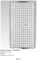
FIG. 3 is a diagram of a current distribution of a floor characteristic mode of an antenna of an electronic device in a conventional technology at 0.8 GHz; -
FIG. 4 is a diagram of a current distribution of a floor characteristic mode of an antenna of an electronic device in a conventional technology at 2.3 GHz; -
FIG. 5 is a schematic diagram of use of an electronic device in a besides head and hand scenario according to an embodiment of this application; -
FIG. 6 is a schematic diagram of a structure of an antenna apparatus in an electronic device according to an embodiment of this application; -
FIG. 7 is a schematic diagram of a structure of an antenna apparatus in an electronic device according to an embodiment of this application; -
FIG. 8 is a schematic diagram of a structure of an antenna apparatus in an electronic device according to an embodiment of this application; -
FIG. 9 is a schematic diagram of a structure of an antenna apparatus in an electronic device according to an embodiment of this application; -
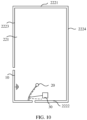
FIG. 10 is a schematic diagram of a structure of an antenna apparatus in an electronic device according to an embodiment of this application; -
FIG. 11 is a schematic diagram of a structure of an antenna apparatus in an electronic device according to an embodiment of this application; -
FIG. 12 is a diagram of a current distribution of a floor characteristic mode of an antenna of an electronic device at 0.9 GHz in a conventional technology; -
FIG. 13 shows a radiation pattern of an antenna of an electronic device at 0.89 GHz in a conventional technology; -
FIG. 14 is a diagram of a current distribution of a floor characteristic mode of an antenna apparatus in an electronic device at 0.9 GHz according to an embodiment of this application; -
FIG. 15 shows a radiation pattern of an antenna apparatus in an electronic device at 0.89 GHz according to an embodiment of this application; -
FIG. 16 is a diagram of a current distribution of a floor characteristic mode of a non-resonant unit of an antenna apparatus in an electronic device at 0.9 GHz according to an embodiment of this application; -
FIG. 17 shows a radiation pattern of a non-resonant unit of an antenna apparatus in an electronic device at 0.89 GHz according to an embodiment of this application; -
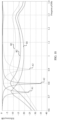
FIG. 18 shows a comparison of each of reflection coefficient curves and radiation efficiency curves of a low-frequency antenna of an electronic device on B28/B5/B8 in a conventional technology; -
FIG. 19 shows a comparison of radiation efficiency on B5 of an antenna in a conventional technology and an antenna apparatus in an electronic device according to an embodiment of this application; -
FIG. 20 shows a comparison of system total efficiency on B28/B5/B8 of an antenna in a conventional technology and an antenna apparatus in an electronic device according to an embodiment of this application; -
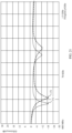
FIG. 21 shows a comparison of reflection coefficient curves of an antenna apparatus in an electronic device and an antenna in a conventional technology; -
FIG. 22 shows a comparison of radiation efficiency of an antenna in a conventional technology and an antenna apparatus in an electronic device according to an embodiment of this application; -
FIG. 23 is a schematic diagram of a structure of an antenna apparatus in an electronic device according to an embodiment of this application; -
FIG. 24 is a schematic diagram of a structure of an antenna apparatus in an electronic device according to an embodiment of this application; -
FIG. 25 is a diagram of a current distribution of a floor characteristic mode of an antenna apparatus in an electronic device at 1.8 GHz according to an embodiment of this application; -
FIG. 26 shows a comparison of reflection coefficient curves, radiation efficiency curves, and system total efficiency of an antenna in a conventional technology and an antenna apparatus in an electronic device according to an embodiment of this application; -
FIG. 27 is a schematic diagram of a structure of an antenna apparatus in an electronic device according to an embodiment of this application; -
FIG. 28 is a schematic diagram of a structure of an antenna apparatus in an electronic device according to an embodiment of this application; and -
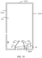
FIG. 29 is a schematic diagram of a structure of an antenna apparatus in an electronic device according to an embodiment of this application. -
- 100-Antenna apparatus; 10-Radiation unit; 101-First radiation unit;
- 102-Second radiation unit; 20-Feed unit; 201-First feed unit;
- 202-Second feed unit; 30-Non-resonant unit; 301-First non-resonant unit;
- 302-Second non-resonant unit; 40-Feed line; 41-First feed line;
- 42-Second feed line; 401-Main feed line; 4011-First end of main feed line;
- 4012-Second end of main feed line; 4013-First conductor; 4014-Second conductor;
- 402-Sub-feed line; 4021-First end of sub-feed line; 4022-Second end of sub-feed line;
- 4023-Inner conductor; 4024-Outer conductor; 4025-Switch;
- L1-First direction; 200-Mobile phone; 21-Display;
- 211-Opening; 22-Middle frame; 221-Metal middle plate;
- 222-Border frame; 2221-Top border frame; 2222-Bottom border frame;
- 2223-Left border frame; 2224-Right border frame; 23-Circuit board;
- 24-Battery; and 25-Rear housing.
- Terms used in implementations of this application are only used to explain specific embodiments of this application, and are not intended to limit this application. The following clearly describes implementations in embodiments of this application with reference to accompanying drawings.
- Embodiments of this application provide an electronic device that may include, but is not limited to, a mobile or fixed terminal having an antenna apparatus, such as a mobile phone, a tablet computer, a notebook computer, an ultra-mobile personal computer (ultra-mobile personal computer, UMPC), a handheld computer, a walkie-talkie, a netbook, a point of sales (Point of sales, POS), a personal digital assistant (personal digital assistant, PDA), a wearable device, a virtual reality device, a wireless USB flash, a Bluetooth speaker/headset, a factory-installed vehicle component, an event data recorder, or a security device.
- In an embodiment of this application, an example in which a
mobile phone 200 is the foregoing electronic device is used for description. Themobile phone 200 provided in the embodiment of this application may be a curved screen mobile phone or a flat screen mobile phone. In the embodiment of this application, the flat screen mobile phone is used as an example for description.FIG. 1 andFIG. 2 respectively show an overall structure and a split structure of themobile phone 200. Adisplay 21 of themobile phone 200 provided in this embodiment of this application may be a waterdrop screen, a notch screen, a full screen, or a punch-hole screen (as shown inFIG. 1 ). For example, thedisplay 21 is provided with anopening 211. The following is described by using the punch-hole screen as an example. - Referring to
FIG. 2 , themobile phone 200 may include thedisplay 21, arear housing 25, and amiddle frame 22 located between thedisplay 21 and therear housing 25. In addition, themobile phone 200 may further include abattery 24, and thebattery 24 is located between themiddle frame 22 and therear housing 25. Thebattery 24 may be disposed on a surface that is of themiddle frame 22 and that faces the rear housing 25 (as shown inFIG. 2 ), or thebattery 24 may be disposed on a surface that is of themiddle frame 22 and that faces thedisplay 21. For example, the surface that is of themiddle frame 22 and that faces therear housing 25 may include a battery compartment (not shown in the figure), and thebattery 24 is mounted in the battery compartment. - In some other examples, the
mobile phone 200 may further include acircuit board 23. Thecircuit board 23 may be disposed on themiddle frame 22, for example, thecircuit board 23 may be disposed on the surface that is of themiddle frame 22 and that faces the rear housing 25 (as shown inFIG. 2 ), or thecircuit board 23 may be disposed on the surface that is of themiddle frame 22 and that faces thedisplay 21. Thedisplay 21 and therear housing 25 are respectively located on two sides of themiddle frame 22. - The
battery 24 may be connected to a charging management module and thecircuit board 23 by using a power management module. The power management module receives an input of thebattery 24 and/or an input of the charging management module, and supplies power to a processor, an internal memory, an external memory, thedisplay 21, a camera module, a communication module, and the like. The power source management module may be further configured to monitor parameters such as a capacity of thebattery 24, a cycle count of thebattery 24, and a state of health (leakage or impedance) of thebattery 24. In some other embodiments, the power management module may alternatively be disposed in a processor of thecircuit board 23. In some other embodiments, the power management module and the charging management module may be disposed in a same component. - When the
mobile phone 200 is a flat screen mobile phone, thedisplay 21 may be an organic light-emitting diode (Organic Light-Emitting Diode, OLED) display, or may be a liquid crystal display (Liquid Crystal Display, LCD). When themobile phone 200 is a curved screen mobile phone, thedisplay 21 may be an OLED display. - Still referring to
FIG. 2 , themiddle frame 22 may be a metal middle frame, the metal middle frame may include at least a metalmiddle plate 221 and ametal border frame 222, and theborder frame 222 is disposed around an outer periphery of the metalmiddle plate 221 for one cycle. Generally, theborder frame 222 may include atop border frame 2221, abottom border frame 2222, aleft border frame 2223, and aright border frame 2224, and thetop border frame 2221, thebottom border frame 2222, theleft border frame 2223, and theright border frame 2224 surround theframe 222 having a square ring structure. A material of the metalmiddle plate 221 includes, but is not limited to, an aluminum plate, aluminum alloy, stainless steel, a steel-aluminum composite die-casting plate, titanium alloy, magnesium alloy, or the like. Theborder frame 222 may be a metal border frame, a ceramic border frame, or a glass border frame. When theborder frame 222 is the metal border frame, a material of the metal border frame includes, but is not limited to, aluminum alloy, stainless steel, a steel-aluminum composite die-casting plate, titanium alloy, or the like. The metalmiddle plate 221 may be connected to theborder frame 222 through clamping, welding, bonding, or integral molding, or the metalmiddle plate 221 may be fixedly connected to theborder frame 222 through injection molding. - Referring to
FIG. 2 , thetop border frame 2221 is disposed opposite to thebottom border frame 2222, theleft border frame 2223 is disposed opposite to theright border frame 2224, thetop border frame 2221 is separately connected to one end of theleft border frame 2223 and one end of theright border frame 2224 at a rounded corner, and thebottom border frame 2222 is separately connected to the other end of theleft border frame 2223 and the other end of theright border frame 2224 at a rounded corner, to jointly form a round-cornered rectangular region. A surface that is of a rear housing and that is grounded is disposed in the round-cornered rectangular region, and is separately connected to thetop border frame 2221, thebottom border frame 2222, theleft border frame 2223, and theright border frame 2224. It may be understood that the surface that is of the rear housing and that is grounded may be therear housing 25 of themobile phone 200. - The
rear housing 25 may be a metal rear housing, a glass rear housing, a plastic rear housing, or a ceramic rear housing. In the embodiment of this application, a material of therear housing 25 is not limited, and is not limited to the foregoing examples either. - It should be noted that, in some examples, the
rear housing 25 of themobile phone 200 may be connected to theborder frame 222 to form a unibody (Unibody) rear housing. For example, themobile phone 200 may include thedisplay 21, the metalmiddle plate 221, and a rear housing. The rear housing may be a unibody (Unibody) rear housing including theborder frame 222 and therear housing 25. In this way, thecircuit board 23 and thebattery 24 are located in space surrounded by the metalmiddle plate 221 and the rear housing. - It may be understood that the structures illustrated in embodiments of this application do not constitute a specific limitation on the
mobile phone 200. In some other embodiments of this application, themobile phone 200 may include more or fewer components than those shown in the figure, or combine some components, or split some components, or have different component arrangements. The components shown in the figure may be implemented by hardware, software, or a combination of software and hardware. - To implement a communication function of the
mobile phone 200, an antenna may be disposed on themobile phone 200, to transmit and receive signals through the antenna. An antenna performance level of themobile phone 200 in an actual use scenario is directly related to actual user experience. Currently, most of themobile phones 200 are industry design (Industry Design, ID) using a metal border frame and glass rear housing. A size of the metal border frame is limited and an antenna environment is limited. In a plurality of frequency bands of the antenna, based on a relationship between a frequency band and wavelength resonance, the lower the frequency is, the longer the required radiator is, and the greater the space requirement is. Therefore, how to improve antenna performance, especially low-frequency antenna performance, in a limited space environment and a radiator length, has become an important problem in research and design of a terminal antenna. - A theory of a characteristic mode is a very important theory during design of the antenna.
FIG. 3 andFIG. 4 show current distributions of a floor characteristic mode of the antenna. It may be learned from the figures that due to resonance, the floor (that is, the metal middle plate 221) has different current distribution on different frequency bands, that is, the floor characteristic modes of a low-frequency antenna and a medium-high-frequency antenna on different frequency bands have respective characteristics. A current flow direction of the low-frequency antenna is in a longitudinal mode (as shown inFIG. 3 ), and a current flow direction of the medium-high-frequency antenna is in a transverse mode (as shown inFIG. 4 ). A characteristic mode of the floor is an inherent characteristic of the floor. Based on a frequency requirement, a required floor characteristic mode is excited, to obtain high antenna efficiency at a corresponding frequency. For example, for a low frequency antenna, high free space (FS) efficiency can be obtained by sufficiently exciting the floor longitudinal mode; and for a medium-high frequency antenna, high FS efficiency can also be obtained by sufficiently exciting the lateral mode. - A conventional terminal antenna has many use scenarios. For example, common use scenarios include besides head and hand (besides head and hand, BHH), besides head (besides head, BH), and hand (hand, H). These scenarios are also common test scenarios for national authentication or operator admission. For example,
FIG. 5 is a schematic diagram of a besides head and hand scenario. However, in these scenarios, the antenna performance changes compared with FS performance. For example, for FS of the low frequency antenna, a good floor longitudinal characteristic mode is needed when the antenna is designed, but the longitudinal characteristic mode in this case will result in great reduction in the hand. However, if the low-frequency antenna has a good floor transverse characteristic mode, small reduction in the hand may be obtained, and hand performance is good, but the FS deteriorates in this case. - Through analysis, for the low frequency antenna, efficiency of the low frequency antenna is improved if the floor longitudinal characteristic mode is additionally assisted and excited. Similarly, for the medium-high frequency antenna, efficiency of the medium-high frequency antenna is improved if the floor transverse characteristic mode is additionally assisted and excited. Based on this, embodiments of this invention provide an antenna apparatus and an electronic device having the antenna apparatus. The antenna apparatus may be used in the electronic device (for example, the mobile phone 200). The antenna apparatus is provided with a non-resonant unit and a feed unit, to respectively feed a radiation unit and a non-resonant unit. Through feeding power distribution design, the non-resonant unit can assist in exciting the floor characteristic mode. In addition, since a size of the non-resonant unit is much smaller than an electrical length required for resonance of an antenna on this frequency band, the non-resonant unit does not generate a resonance curve on a resonance curve and has no resonance point, to improve radiation efficiency of the antenna without generating new resonance, so as to improve a use effect of a user.
- It should be noted that the antenna apparatus provided in this application is used in an electronic device using any one or more of the following communication technologies, for example, a long term evolution (long term evolution, LTE) communication technology, a Wi-Fi communication technology, a 5G communication technology, a SUB-6G communication technology, and another communication technology in the future.
- The following describes a specific structure of the antenna apparatus with reference to specific accompanying drawings (the following embodiments do not highlight a need for a communication network, and describe an operation characteristic of the antenna apparatus only based on a frequency).
- As shown in
FIG. 6 to FIG. 8 , an embodiment of this application provides anantenna apparatus 100. Theantenna apparatus 100 is used in amobile phone 200. Themobile phone 200 may include adisplay 21, arear housing 25, and a middle frame 22 (referring toFIG. 2 ) located between thedisplay 21 and therear housing 25. Theantenna apparatus 100 may include at least oneradiation unit 10, at least onefeed unit 20, and at least onenon-resonant unit 30, and thefeed unit 20 separately feeds theradiation unit 10 and thenon-resonant unit 30. - A size of the
non-resonant unit 30 may be less than 1/8λ, where λ is a wavelength corresponding to a resonance frequency of theradiation unit 10. It should be noted that the size of thenon-resonant unit 30 is much smaller than an electrical length required for resonance of theradiation unit 10 on this frequency band, to ensure that thenon-resonant unit 30 does not generate a resonance curve on a reflection coefficient curve (S 11) and has no resonance point. Therefore, even if thenon-resonant unit 30 is removed, the resonance curve and a quantity of resonance points on S11 do not change. - For example, as shown in
FIG. 6 , the size of thenon-resonant unit size 30 may be 8 mm x 9 mm, which is less than a resonant length of theradiation unit 10 on this frequency band. A 1/4 wavelength at a low frequency is 75 mm @ 1 GHz. It may be understood that thenon-resonant unit 30 may be a metal layer or may be a border frame metal branch, and this is not limited in this embodiment of this application, and is not limited to the foregoing example either. - In this embodiment of this application, a
border frame 222 may be a metal border frame, the metal border frame may form a metal border frame antenna, and the metal border frame antenna is used as the at least oneradiation unit 10 in theantenna apparatus 100. Specifically, the metal border frame antenna may be a radiator located on the metal border frame, and the radiator is formed by opening a slot in the metal border frame, in other words, the metal border frame antenna is a slot antenna formed by slotting in the metal border frame. The slot antenna may include a first part, a second part, and a third part separated by slots, and a non-conductive material may be filled between the first part and the second part, between the second part and the third part, and between the third part and the first part. - In an actual application, positions of the slots may be varied as required, and the slots may be filled with a non-conductive material (such as plastic), to ensure integrity of the metal border frame in appearance. By flexibly providing opening positions of the slots on the metal border frame, appearance design with different requirements may be implemented while ensuring radiation performance of the antenna, thereby improving product quality of the
mobile phone 200. - A feed point and a ground point of the
feed unit 20 may be respectively electrically connected to thenon-resonant unit 30 and a metalmiddle plate 221 used as a floor in themobile phone 200. It may be understood that thenon-resonant unit 30 is configured to assist in exciting the floor characteristic mode, and thenon-resonant unit 30 assists in exciting the floor longitudinal characteristic mode when theradiation unit 10 is a low frequency radiation unit. The non-resonant unit 300 assists in exciting the floor transverse characteristic mode when theradiation unit 10 is a medium-high frequency radiation unit. - A current flow direction of the low-frequency radiation unit is in a longitudinal mode, and a current flow direction of the medium-high frequency radiation unit is in a transverse mode, so that high antenna efficiency at a corresponding frequency can be obtained by exciting a required floor characteristic mode. That is, for the low-frequency radiation unit, high radiation efficiency can be obtained by sufficiently exciting the floor longitudinal mode; and for the medium-high frequency radiation unit, high radiation efficiency can also be obtained by sufficiently exciting the transverse mode.
- In a possible implementation, an orthographic projection that is of the
non-resonant unit 30 and that is in a first direction L1 may be located in the metalmiddle plate 221, and the first direction L1 is the direction perpendicular to a plane in which the metalmiddle plate 221 is located. For example, thenon-resonant unit 30 may be located above the metalmiddle plate 221, so that thefeed unit 20 is separately connected to thenon-resonant unit 30 and a floor (that is, the metal middle plate 221) below thenon-resonant unit 30 through a power distribution of a feed connection, thereby assisting in exciting the floor characteristic mode. - As an optional implementation, the
feed unit 20 may be electrically connected to thenon-resonant unit 30 and the metalmiddle plate 221 by using afeed line 40. Through a line power distribution of thefeed line 40 for the feed connection, thefeed unit 20 is connected to each of thenon-resonant unit 30 and the floor (that is, the metal middle plate 221) below thenon-resonant unit 30 by using thefeed line 40, thereby assisting in exciting the floor characteristic mode. - As shown in
FIG. 8 andFIG. 9 , eachfeed line 40 may include amain feed line 401 and asub-feed line 402. Themain feed line 401 and thesub-feed line 402 each include a signal line and a ground line. A signal line at afirst end 4011 of the main feed line is electrically connected to thefeed unit 20, a signal line at asecond end 4012 of the main feed line is electrically connected to theradiation unit 10, and a ground line of themain feed line 401 is grounded. A signal line and a ground line at afirst end 4021 of the sub-feed line are electrically connected to the signal line and the ground line of themain feed line 401, and a signal line and a ground line at asecond end 4022 of the sub-feed line are electrically connected to thenon-resonant unit 30 and the metalmiddle plate 221 respectively. In this way, thefeed unit 20 can separately feed theradiation unit 10 and thenon-resonant unit 30, and efficiency of the antenna can be effectively improved through a power distribution at a feed location and a connection to thenon-resonant unit 30 and the floor (that is, the metal middle plate 221) at thenon-resonant unit 30. - In a possible implementation, still referring to
FIG. 8 , thesub-feed line 402 may be a coaxial line. Specifically, thesub-feed line 402 may include anouter conductor 4024 and aninner conductor 4023, theouter conductor 4024 is wrapped outside theinner conductor 4023, theinner conductor 4023 is the signal line of thesub-feed line 402, and theouter conductor 4024 is the ground line of thesub-feed line 402. One end of theinner conductor 4023 is electrically connected to the signal line of themain feed line 401, and the other end of theinner conductor 4023 is electrically connected to thenon-resonant unit 30. One end of theouter conductor 4024 is electrically connected to the ground line of themain feed line 401, and the other end of theouter conductor 4024 is electrically connected to the metalmiddle plate 221. Theinner conductor 4023 of thesub-feed line 402 is electrically connected to thenon-resonant unit 30, and theouter conductor 4024 of thesub-feed line 402 is electrically connected to the floor (that is, the metal middle plate 221) at thenon-resonant unit 30, so that while assisting in exciting the floor characteristic mode, the metalmiddle plate 221 connected to theouter conductor 4024 can provide a specific shielding effect for thenon-resonant unit 30 connected to theinner conductor 4023. - In addition, as shown in
FIG. 8 , themain feed line 401 may be a microstrip line. Specifically, themain feed line 401 may include afirst conductor 4013 and asecond conductor 4014. Thefirst conductor 4013 is the signal line of themain feed line 401, thesecond conductor 4014 is the ground line of themain feed line 401, and thefirst conductor 4013 is separated from thesecond conductor 4014. In this way, transmission of a power supply signal and a ground signal between thefeed unit 20 and theradiation unit 10 can be ensured. - It should be noted that the
first end 4011 of the main feed line may include a first end of thefirst conductor 4013 and a first end of thesecond conductor 4014. For ease of identification, inFIG. 9 , the first end of thefirst conductor 4013 is used as an example to show thefirst end 4011 of the main feed line. - In this embodiment of this application, the
non-resonant unit 30 may be disposed at a position as shown inFIG. 8 , or may be disposed at a position as shown inFIG. 10 orFIG. 11 . A specific position of thenon-resonant unit 30 is not limited in this embodiment of this application, and is not limited to the forgoing example either. It should be noted that theradiation unit 10 may be a low-frequency radiation unit. -
FIG. 12 andFIG. 13 are respectively a diagram of a current distribution and a pattern of an antenna in a conventional technology.FIG. 14 andFIG. 15 are respectively a diagram of an overall current distribution and an overall pattern of anantenna apparatus 100 when anon-resonant unit 30 is introduced into theantenna apparatus 100 according to an embodiment of this application.FIG. 16 andFIG. 17 are respectively a diagram of a current distribution and a pattern of anon-resonant unit 30 introduced into anantenna apparatus 100 according to an embodiment of this application. Through comparison, it can be learned that thenon-resonant unit 30 introduced into theantenna apparatus 100 in this embodiment of this application does not change the overall current distribution and pattern characteristic of theantenna apparatus 100, but the current distribution on thenon-resonant unit 30 significantly excites the floor characteristic mode better, and excitation of such characteristic mode is beneficial for improving antenna efficiency. -
FIG. 18 shows a comparison of each of reflection coefficient curves and radiation efficiency curves of an antenna of an electronic device on B28/B5/B8 in a conventional technology. InFIG. 18 , A1 is a reflection coefficient curve obtained by tuning an antenna on the B28 band, B1 is a radiation efficiency curve obtained by tuning the antenna on the B28 band, A2 is a reflection coefficient curve obtained by tuning an antenna on the B5 band, B2 is a radiation efficiency curve obtained by tuning the antenna on the B5 band, A3 is a reflection coefficient curve obtained by tuning an antenna on the B8 band, and B3 is a radiation efficiency curve obtained by tuning the antenna on the B8 band. A frequency band covered by B28 is 703 MHz to 748 MHz, a frequency band covered by B5 is 824 MHz to 849 MHz, and a frequency band covered by B8 is 880 MHz to 915 MHz. -
FIG. 19 andFIG. 20 show a comparison of radiation efficiency and system efficiency of an antenna after anon-resonant unit 30 is introduced according to an embodiment of this application and radiation efficiency and system efficiency of an antenna without using a solution in an embodiment of this application. InFIG. 19 , C1 is a radiation efficiency curve of an antenna in a conventional technology, and C2 is a radiation efficiency curve of anantenna apparatus 100 according to an embodiment of this application. InFIG. 20 , D1 is a system efficiency curve when theantenna apparatus 100 in this embodiment of this application is on the B28 band, D2 is a system efficiency curve when theantenna apparatus 100 in this embodiment of this application is on the B5 band, D3 is a system efficiency curve when theantenna apparatus 100 in this embodiment of this application is on the B8 band, E1 is a system efficiency curve when the antenna in the conventional technology is on the B28 band, E2 is a system efficiency curve when the antenna in the conventional technology is on the B5 band, and E3 is a system efficiency curve when the antenna in the conventional technology is on the B8 band. - Through comparison, it may be apparently seen that the
non-resonant unit 30 is introduced, so that antenna efficiency can be effectively improved through a power distribution at a feed location and a connection of thenon-resonant unit 30 and the floor (the metal middle plate 221) at thenon-resonant unit 30. Specifically, at 700 MHz, the radiation efficiency of theantenna apparatus 100 in this embodiment of this application is 1.5 dB higher than the radiation efficiency of the antenna in the conventional technology. At 800 MHz, the radiation efficiency of theantenna apparatus 100 in this embodiment of this application is 1.4 dB higher than the radiation efficiency of the antenna in the conventional technology. At 900 MHz, the radiation efficiency of theantenna apparatus 100 in this embodiment of this application is 1.3 dB higher than the radiation efficiency of the antenna in the conventional technology. - In addition, it should be noted that a result consistent with a simulation result can be obtained through debugging and verifying on an actual project.
FIG. 8 is a schematic diagram of an experimental fixture for verifying on an actual project. InFIG. 8 , the power distribution is performed at the feed location, theinner conductor 4023 of thefeed line 40 is connected to thenon-resonant unit 30, theouter conductor 4024 of thefeed line 40 is connected to a middle frame of the floor at thenon-resonant unit 30, and thenon-resonant unit 30 may be a copper sheet of 10 mm x 10 mm. -
FIG. 21 andFIG. 22 respectively show a reflection coefficient curve and a radiation efficiency curve actually measured by an actual fixture. InFIG. 21 , F1 is a reflection coefficient curve of an antenna in a conventional technology, and F2 is a reflection coefficient curve of anantenna apparatus 100 according to an embodiment of this application. InFIG. 22 , G1 is a radiation efficiency curve of an antenna in a conventional technology, and G2 is a radiation efficiency curve of anantenna apparatus 100 according to an embodiment of this application. An actual measurement result shows that thenon-resonant unit 30 introduced in this embodiment of this application can effectively improve the antenna efficiency without increasing resonance of S11. A frequency-deviation phenomenon occurring therein because a distributed capacitor of thenon-resonant unit 30 and the middle frame of floor (the metal middle plate 221) is loaded to the feed location and cause capacitor loading, and this frequency deviation can be easily adjusted through tuning. - In addition, the method for improving the antenna efficiency by introducing the non-resonant unit to assist in exciting the floor characteristic mode mentioned in this invention patent can also be applied to a medium-high frequency antenna. As shown in
FIG. 23 orFIG. 24 , a non-resonant unit is added to the medium-high frequency antenna, and an excited floor characteristic mode current is shown inFIG. 25 . The floor characteristic mode current assisted and excited by thenon-resonant unit 30 is completely consistent with a medium-high frequency floor characteristic mode current shown inFIG. 4 . -
FIG. 26 shows a comparison of efficiency benefits of introducing anon-resonant unit 30 into an antenna apparatus 100 (that is, a structure shown inFIG. 23 orFIG. 24 ) according to an embodiment of this application. InFIG. 26 , L1 is a reflection coefficient curve of an antenna in a conventional technology, L2 is a reflection coefficient curve of theantenna apparatus 100 according to an embodiment of this application, M1 is a radiation efficiency curve of the antenna in the conventional technology, M2 is a radiation efficiency curve of theantenna apparatus 100 according to an embodiment of this application, N1 is a system total efficiency curve of the antenna in the conventional technology, and N2 is a system total efficiency curve of theantenna apparatus 100 according to an embodiment of this application. It may be apparently seen from the efficiency curve, compared with the conventional technology, in theantenna apparatus 100 provided in this embodiment of this application, the antenna efficiency of the medium-high frequency can also be significantly improved, and the antenna efficiency can be improved by 1.7 dB at 1.8 GHz, thereby improving antenna performance. - It should be noted that, in this embodiment of this application, the
radiation unit 10 may be a metal border frame antenna, and thenon-resonant unit 30 may be disposed close to the metal border frame antenna. Thenon-resonant unit 30 is disposed close to the metal border frame antenna, so that a length of thefeed line 40 can be reduced to some extent, thereby reducing costs and improving reliability. - In addition, in some embodiments, a quantity of
non-resonant units 30 is one, and a quantity offeed lines 40 may be at least two. As shown inFIG. 27 , the at least onefeed unit 20 may include afirst feed unit 201 and asecond feed unit 202. A feed point and a ground point of thefirst feed unit 201 may be electrically connected to thenon-resonant unit 30 and the metalmiddle plate 221 by using afirst feed line 41 of the at least twofeed lines 40, and a feed point and a ground point of thesecond feed unit 202 may be electrically connected to thenon-resonant unit 30 and the metalmiddle plate 221 by using asecond feed line 42 of the at least twofeed lines 40. - The at least one
radiation unit 10 may include afirst radiation unit 101 and asecond radiation unit 102. The signal line at thefirst end 4011 of the main feed line of thefirst feed line 41 is electrically connected to thefirst feed unit 201, the signal line at thesecond end 4012 of the main feed line of thefirst feed line 41 is electrically connected to thefirst radiation unit 101, and the ground line of themain feed line 401 of thefirst feed line 41 is grounded. The signal line and the ground line at thefirst end 4021 of the sub-feed line of thefirst feed line 41 are electrically connected to the signal line and the ground line of themain feed line 401 of thefirst feed line 41, and the signal line and the ground line at thesecond end 4022 of the sub-feed line of thefirst feed line 41 are electrically connected to thenon-resonant unit 30 and the metalmiddle plate 221 respectively. - The signal line at the
first end 4011 of the main feed line of thesecond feed line 42 is electrically connected to thesecond feed unit 202, the signal line at thesecond end 4012 of the main feed line of thesecond feed line 42 is electrically connected to thesecond radiation unit 102, and the ground line of themain feed line 401 of thesecond feed line 42 is grounded. The signal line and the ground line at thefirst end 4021 of the sub-feed line of thesecond feed line 42 are electrically connected to the signal line and the ground line of themain feed line 401 of thesecond feed line 42, and the signal line and the ground line at thesecond end 4022 of the sub-feed line of thesecond feed line 42 are electrically connected to thenon-resonant unit 30 and the metalmiddle plate 221 respectively. - In this way, the
first feed unit 201 is connected to thefirst radiation unit 101, thenon-resonant unit 30, and the floor below the non-resonant unit 30 (that is, the metal middle plate 221) by using thefirst feed line 41, thesecond feed unit 202 is connected to thesecond radiation unit 102, thenon-resonant unit 30, and the floor below the non-resonant unit 30 (that is, the metal middle plate 221) by using thesecond feed line 42. That is, through a line power distribution, thefirst feed unit 201 feeds thefirst radiation unit 101 and thenon-resonant unit 30 by using thefirst feed line 41, and thesecond feed unit 202 feeds thesecond radiation unit 102 and thenon-resonant unit 30 by using thesecond feed line 42, so that thenon-resonant unit 30 can assist thefirst radiation unit 101 and thesecond radiation unit 102 in exciting the floor characteristic mode. - As an optional implementation, in
FIG. 27 , thefirst radiation unit 101 may be a low-frequency radiation unit, and thesecond radiation unit 102 may be a medium-frequency radiation unit. Certainly, in some other embodiments, thefirst radiation unit 101 and thesecond radiation unit 102 may be low frequency radiation units, or thefirst radiation unit 101 and thesecond radiation unit 102 may be medium-high frequency radiation units. - Further, in another embodiment, as shown in
FIG. 28 , a quantity ofnon-resonant units 30 may be two, and the at least onenon-resonant unit 30 may include a firstnon-resonant unit 301 and a secondnon-resonant unit 302. A quantity offeed lines 40 may be at least two, and the at least onefeed unit 20 may include afirst feed unit 201 and asecond feed unit 202. A feed point and a ground point of thefirst feed unit 201 may be electrically connected to the firstnon-resonant unit 301 and the metalmiddle plate 221 by using afirst feed line 41 of the at least twofeed lines 40, and a feed point and a ground point of thesecond feed unit 202 may be electrically connected to the secondnon-resonant unit 302 and the metalmiddle plate 221 by using asecond feed line 42 of the at least twofeed lines 40. - Similarly, the at least one
radiation unit 10 may include afirst radiation unit 101 and asecond radiation unit 102. The signal line at thefirst end 4011 of the main feed line of thefirst feed line 41 is electrically connected to thefirst feed unit 201, the signal line at thesecond end 4012 of the main feed line of thefirst feed line 41 is electrically connected to thefirst radiation unit 101, and the ground line of themain feed line 401 of thefirst feed line 41 is grounded. The signal line and the ground line at thefirst end 4021 of the sub-feed line of thefirst feed line 41 are electrically connected to the signal line and the ground line of themain feed line 401 of thefirst feed line 41, and the signal line and the ground line at thesecond end 4022 of the sub-feed line of thefirst feed line 41 are electrically connected to the firstnon-resonant unit 301 and the metalmiddle plate 221 respectively. - The signal line at the
first end 4011 of the main feed line of thesecond feed line 42 is electrically connected to thesecond feed unit 202, the signal line at thesecond end 4012 of the main feed line of thesecond feed line 42 is electrically connected to thesecond radiation unit 102, and the ground line of themain feed line 401 of thesecond feed line 42 is grounded. The signal line and the ground line at thefirst end 4021 of the sub-feed line of thesecond feed line 42 are electrically connected to the signal line and the ground line of themain feed line 401 of thesecond feed line 42, and the signal line and the ground line at thesecond end 4022 of the sub-feed line of the second feed line 45 are electrically connected to the secondnon-resonant unit 302 and the metalmiddle plate 221 respectively. - In this way, the
first feed unit 201 is connected to thefirst radiation unit 101, the firstnon-resonant unit 301, and the floor below the first non-resonant unit 301 (that is, the metal middle plate 221) by using thefirst feed line 41, thesecond feed unit 202 is connected to thesecond radiation unit 102, the secondnon-resonant unit 302, and the floor below the second non-resonant unit 302 (that is, the metal middle plate 221) by using thesecond feed line 42. That is, through a line power distribution, thefirst feed unit 201 feeds thefirst radiation unit 101 and the firstnon-resonant unit 301 by using thefirst feed line 41, and thesecond feed unit 202 feeds thesecond radiation unit 102 and the secondnon-resonant unit 302 by using thesecond feed line 42, so that the firstnon-resonant unit 301 can assist thefirst radiation unit 101 in exciting the floor characteristic mode, and the secondnon-resonant unit 302 can assist thesecond radiation unit 102 in exciting the floor characteristic mode. - In addition, as an optional implementation, the
sub-feed line 402 may be provided with a switch 4025 (as shown inFIG. 29 ), theswitch 4025 is configured to select to turn on the non-resonant unit 30 (that is, the firstnon-resonant unit 301 or the second non-resonant unit 302) on thesub-feed line 402. Theswitch 4025 can control themain feed line 401 and thenon-resonant unit 30 to be connected or disconnected, thereby ensuring flexible use. For example, if thenon-resonant unit 30 is not required to assist in exciting the floor characteristic mode, theswitch 4025 can be turned on; or if thenon-resonant unit 30 is required to assist in exciting the floor characteristic mode, theswitch 4025 can be turned off. - In descriptions of embodiments, it should be noted that, unless otherwise expressly specified and limited, the terms "installation", "connect", and "connection" should be understood in a broad sense, for example, may be a fixed connection, or may be an indirect connection by using an intermediate medium, or may be a communication between two elements or an interaction between two elements. A person of ordinary skill in the art can understand specific meanings of the foregoing terms in embodiments of this application based on a specific situation.
- The apparatus or element referred to in or implied in embodiments of this application needs to have a specific orientation, be constructed and operated in a specific orientation, and therefore cannot be construed as a limitation on embodiments of this specification. In the descriptions of embodiments of this application, "a plurality of" means two or more, unless otherwise specifically defined.
- In the specification of embodiments, claims, and accompanying drawings of this application, the terms "first", "second", "third", "fourth", and the like (if existent) are intended to distinguish between similar objects but do not necessarily indicate a specific order or sequence. It should be understood that the data termed in such a way are interchangeable in proper circumstances, so that embodiments described herein can be implemented in orders except the order illustrated or described herein. In addition, the terms "may include" and "have", and any variations thereof are intended to cover non-exclusive inclusions. For example, a process, a method, a system, a product, or a device that includes a series of steps or units is not necessarily limited to those steps or units that are clearly listed, but may include other steps or units that are not clearly listed or are inherent to the process, method, product, or device.
- Finally, it should be noted that the foregoing embodiments are only used to illustrate the technical solutions of embodiments of this application, but are not used to limit this application. Although embodiments of this application has been described in detail with reference to the foregoing embodiments, it should be understood by a person of ordinary skill in the art that the technical solutions described in the foregoing embodiments may still be modified, or some or all technical features thereof are equivalently replaced. These modifications or replacements do not make the essence of the corresponding technical solutions depart from the scope of the technical solutions of embodiments of this application.
Claims (17)
- An antenna apparatus, applied to an electronic device, wherein the antenna apparatus comprises:at least one radiation unit, at least one feed unit, and at least one non-resonant unit, wherein the feed unit directly feeds the radiation unit and the non-resonant unit separately; anda size of the non-resonant unit is less than 1/8λ, and λ is a wavelength corresponding to a resonance frequency of the radiation unit.
- The antenna apparatus according to claim 1, wherein a feed point and a ground point of the feed unit are respectively electrically connected to the non-resonant unit and a metal middle plate used as a floor in the electronic device.
- The antenna apparatus according to claim 2, wherein the non-resonant unit is configured to assist in exciting a floor characteristic mode; and when the radiation unit is a low-frequency radiation unit, the non-resonant unit assists in exciting a floor longitudinal characteristic mode; or when the radiation unit is a medium-high frequency radiation unit, the non-resonant unit assists in exciting a floor transverse characteristic mode.
- The antenna apparatus according to claim 2 or 3, wherein an orthographic projection that is of the non-resonant unit and that is in a first direction is located in the metal middle plate; and
the first direction is the direction perpendicular to a plane in which the metal middle plate is located. - The antenna apparatus according to any one of claims 2 to 4, wherein the feed unit is electrically connected to each of the non-resonant unit and the metal middle plate by using a feed line.
- The antenna apparatus according to claim 5, wherein each feed line comprises a main feed line and a sub-feed line, the main feed line and the sub-feed line each comprise a signal line and a ground line, a signal line at a first end of the main feed line is electrically connected to the feed unit, and a signal line at a second end of the main feed line is electrically connected to the radiation unit; and the ground line of the main feed line is grounded; and
a signal line and a ground line at a first end of the sub-feed line are electrically connected to the signal line and the ground line of the main feed line, and a signal line and a ground line at a second end of the sub-feed line are electrically connected to the non-resonant unit and the metal middle plate respectively. - The antenna apparatus according to claim 6, wherein the sub-feed line is a coaxial line and comprises an outer conductor and an inner conductor; and the outer conductor is wrapped outside the inner conductor, the inner conductor is the signal line, and the outer conductor is the ground line; and
one end of the inner conductor is electrically connected to the signal line of the main feed line, and the other end of the inner conductor is electrically connected to the non-resonant unit; and one end of the outer conductor is electrically connected to the ground line of the main feed line, and the other end of the outer conductor is electrically connected to the metal middle plate. - The antenna apparatus according to claim 6 or 7, wherein the main feed line is a microstrip line comprising a first conductor and a second conductor, the first conductor is the signal line, the second conductor is the ground line, and the first conductor is separated from the second conductor.
- The antenna apparatus according to any one of claims 6 to 8, wherein a quantity of non-resonant units is one;a quantity of feed lines is at least two; the at least one feed unit comprises a first feed unit and a second feed unit; anda feed point and a ground point of the first feed unit are respectively electrically connected to the non-resonant unit and the metal middle plate by using a first feed line of the at least two feed lines, and a feed point and a ground point of the second feed unit are respectively electrically connected to the non-resonant unit and the metal middle plate by using a second feed line of the at least two feed lines.
- The antenna apparatus according to claim 9, wherein the at least one radiation unit comprises a first radiation unit and a second radiation unit;the signal line at the first end of the main feed line of the first feed line is electrically connected to the first feed unit, and the signal line at the second end of the main feed line of the first feed line is electrically connected to the first radiation unit; the ground line of the main feed line of the first feed line is grounded; and the signal line and the ground line at the first end of the sub-feed line of the first feed line are electrically connected to the signal line and the ground line of the main feed line of the first feed line, and the signal line and the ground line at the second end of the sub-feed line of the first feed line are electrically connected to the non-resonant unit and the metal middle plate respectively; andthe signal line at the first end of the main feed line of the second feed line is electrically connected to the second feed unit, and the signal line at the second end of the main feed line of the second feed line is electrically connected to the second radiation unit; the ground line of the main feed line of the second feed line is grounded; and the signal line and the ground line at the first end of the sub-feed line of the second feed line are electrically connected to the signal line and the ground line of the main feed line of the second feed line, and the signal line and the ground line at the second end of the sub-feed line of the second feed line are electrically connected to the non-resonant unit and the metal middle plate respectively.
- The antenna apparatus according to any one of claims 6 to 8, wherein a quantity of non-resonant units is two;the at least one non-resonant unit comprises a first non-resonant unit and a second non-resonant unit;a quantity of feed lines is at least two; the at least one feed unit comprises a first feed unit and a second feed unit; andthe first feed unit is electrically connected to each of the first non-resonant unit and the metal middle plate by using a first feed line of the at least two feed lines, and the second feed unit is electrically connected to each of the second non-resonant unit and the metal middle plate by using a second feed line of the at least two feed lines.
- The antenna apparatus according to claim 11, wherein the at least one radiation unit comprises a first radiation unit and a second radiation unit;the signal line at the first end of the main feed line of the first feed line is electrically connected to the first feed unit, and the signal line at the second end of the main feed line of the first feed line is electrically connected to the first radiation unit; the ground line of the main feed line of the first feed line is grounded; and the signal line and the ground line at the first end of the sub-feed line of the first feed line are electrically connected to the signal line and the ground line of the main feed line of the first feed line, and the signal line and the ground line at the second end of the sub-feed line of the first feed line are electrically connected to the first non-resonant unit and the metal middle plate respectively; andthe signal line at the first end of the main feed line of the second feed line is electrically connected to the second feed unit, and a signal line at a second end of the main feed line of the second feed line is electrically connected to the second radiation unit; the ground line of the main feed line of the second feed line is grounded; and the signal line and the ground line at the first end of the sub-feed line of the second feed line are electrically connected to the signal line and the ground line of the main feed line of the second feed line, and the signal line and the ground line at the second end of the sub-feed line of the second feed line are electrically connected to the second non-resonant unit and the metal middle plate respectively.
- An antenna apparatus according to claim 10 or 12, wherein the first radiation unit is a low frequency radiation unit, and the second radiation unit is a medium-high frequency radiation unit.
- The antenna apparatus according to any one of claims 6 to 13, wherein the sub-feed line is provided with a switch for selecting to turn on the non-resonant unit on the sub-feed line.
- The antenna apparatus according to any one of claims 1 to 14, wherein the radiation unit is a metal border frame antenna, and the non-resonant unit is disposed close to the metal border frame antenna.
- An electronic device, wherein the electronic device comprises at least a display, a rear housing, and a middle frame between the display and the rear housing, and further comprises the antenna apparatus according to any one of claims 1 to 15.
- The electronic device according to claim 16, wherein the middle frame is a metal middle frame, the metal middle frame comprises at least a metal border frame and a metal middle plate, and the metal border frame is disposed around an outer periphery of the metal middle plate; and
the metal border frame forms a metal border frame antenna, and the metal border frame antenna is used as at least one radiation unit in the antenna apparatus.
Applications Claiming Priority (2)
| Application Number | Priority Date | Filing Date | Title |
|---|---|---|---|
| CN202110391085.0A CN113258268B (en) | 2021-04-12 | 2021-04-12 | Antenna device and electronic apparatus |
| PCT/CN2022/073600 WO2022218005A1 (en) | 2021-04-12 | 2022-01-24 | Antenna apparatus and electronic device |
Publications (3)
| Publication Number | Publication Date |
|---|---|
| EP4191791A1 true EP4191791A1 (en) | 2023-06-07 |
| EP4191791A4 EP4191791A4 (en) | 2024-05-15 |
| EP4191791B1 EP4191791B1 (en) | 2025-01-01 |
Family
ID=77220647
Family Applications (1)
| Application Number | Title | Priority Date | Filing Date |
|---|---|---|---|
| EP22787236.3A Active EP4191791B1 (en) | 2021-04-12 | 2022-01-24 | Antenna apparatus and electronic device |
Country Status (4)
| Country | Link |
|---|---|
| US (1) | US12381322B2 (en) |
| EP (1) | EP4191791B1 (en) |
| CN (1) | CN113258268B (en) |
| WO (1) | WO2022218005A1 (en) |
Families Citing this family (1)
| Publication number | Priority date | Publication date | Assignee | Title |
|---|---|---|---|---|
| CN113258268B (en) | 2021-04-12 | 2022-11-01 | 荣耀终端有限公司 | Antenna device and electronic apparatus |
Family Cites Families (17)
| Publication number | Priority date | Publication date | Assignee | Title |
|---|---|---|---|---|
| US6734825B1 (en) * | 2002-10-28 | 2004-05-11 | The National University Of Singapore | Miniature built-in multiple frequency band antenna |
| KR20050010549A (en) * | 2003-07-21 | 2005-01-28 | 엘지전자 주식회사 | minimum size antenna for UWB communication |
| JP5442428B2 (en) * | 2009-12-25 | 2014-03-12 | 京セラ株式会社 | Duplexer |
| CN102110900B (en) | 2010-12-27 | 2014-07-02 | 中兴通讯股份有限公司 | Array antenna of mobile terminal and implementation method of array antenna |
| CN102280696A (en) * | 2011-04-28 | 2011-12-14 | 上海交通大学 | Half-wave transmission decoupling small-space microstrip array antenna |
| US9496608B2 (en) * | 2013-04-17 | 2016-11-15 | Apple Inc. | Tunable multiband antenna with passive and active circuitry |
| CN103825075A (en) | 2014-01-24 | 2014-05-28 | 张家港保税区国信通信有限公司 | T-shaped branch loading built-in antenna combiner |
| TWI536670B (en) | 2014-04-25 | 2016-06-01 | 國立中山大學 | Communication device and combined-type dual-wideband antenna element therein |
| CN104241862A (en) | 2014-09-19 | 2014-12-24 | 东南大学 | Broad band low-side-lobe antenna based on super surface |
| DE112017004788T5 (en) * | 2016-11-29 | 2019-06-13 | Murata Manufacturing Co., Ltd. | ANTENNA DEVICE AND ELECTRONIC EQUIPMENT |
| TWI678028B (en) * | 2017-12-12 | 2019-11-21 | 群邁通訊股份有限公司 | Antenna structure and wireless communication device with same |
| CN110556620B (en) * | 2018-06-01 | 2021-07-09 | 华为技术有限公司 | Antennas and Mobile Terminals |
| CN111628298B (en) * | 2019-02-27 | 2022-03-11 | 华为技术有限公司 | Common Antenna and Electronic Equipment |
| US20200279469A1 (en) * | 2019-02-28 | 2020-09-03 | 9013733 Canada Inc. | Radio frequency detector |
| CN111029729A (en) * | 2019-12-24 | 2020-04-17 | 西安易朴通讯技术有限公司 | Antenna assembly and electronic equipment |
| CN111641040B (en) | 2020-04-20 | 2022-02-22 | 西安电子科技大学 | Dual-port mobile terminal antenna with self-decoupling characteristic |
| CN113258268B (en) | 2021-04-12 | 2022-11-01 | 荣耀终端有限公司 | Antenna device and electronic apparatus |
-
2021
- 2021-04-12 CN CN202110391085.0A patent/CN113258268B/en active Active
-
2022
- 2022-01-24 EP EP22787236.3A patent/EP4191791B1/en active Active
- 2022-01-24 US US18/044,639 patent/US12381322B2/en active Active
- 2022-01-24 WO PCT/CN2022/073600 patent/WO2022218005A1/en not_active Ceased
Also Published As
| Publication number | Publication date |
|---|---|
| CN113258268A (en) | 2021-08-13 |
| US12381322B2 (en) | 2025-08-05 |
| EP4191791B1 (en) | 2025-01-01 |
| US20240297436A1 (en) | 2024-09-05 |
| CN113258268B (en) | 2022-11-01 |
| EP4191791A4 (en) | 2024-05-15 |
| WO2022218005A1 (en) | 2022-10-20 |
Similar Documents
| Publication | Publication Date | Title |
|---|---|---|
| US9196948B2 (en) | Antenna system for wireless terminal devices | |
| EP4243203B1 (en) | Antenna apparatus and electronic device | |
| CN115842238B (en) | An electronic device | |
| CN107431271A (en) | Multiband antenna on Wireless Telecom Equipment surface | |
| EP3246989B1 (en) | Multi-frequency antenna and terminal device | |
| US20140218250A1 (en) | Case and electronic apparatus | |
| TW201824640A (en) | Mobile device and manufacturing method thereof | |
| US20220021105A1 (en) | Antenna module and electronc device using the same | |
| US20160233581A1 (en) | Electronic device including multiband antenna using persistent conductive border | |
| CN108879112B (en) | Antenna array and terminal | |
| US12381322B2 (en) | Antenna apparatus and electronic device | |
| CN108258399B (en) | Antenna and communication equipment | |
| KR20140100384A (en) | Case and electronic apparatus | |
| US12562462B2 (en) | Electronic assembly and electronic device | |
| US12562477B2 (en) | Antenna and electronic device | |
| CN117977160A (en) | Antenna assembly and electronic equipment | |
| CN114156633B (en) | Low SAR antenna device and electronic equipment | |
| TWI550957B (en) | Mobile communication device having an antenna | |
| TWI549364B (en) | Communication device | |
| CN121307478A (en) | Antenna devices and electronic equipment | |
| CN121149655A (en) | Antenna components and electronic devices | |
| US20240021974A1 (en) | Electronic Device | |
| CN121642516A (en) | electronic devices | |
| CN121307476A (en) | electronic devices | |
| CN118472611A (en) | Antenna device and electronic device |
Legal Events
| Date | Code | Title | Description |
|---|---|---|---|
| STAA | Information on the status of an ep patent application or granted ep patent |
Free format text: STATUS: THE INTERNATIONAL PUBLICATION HAS BEEN MADE |
|
| PUAI | Public reference made under article 153(3) epc to a published international application that has entered the european phase |
Free format text: ORIGINAL CODE: 0009012 |
|
| STAA | Information on the status of an ep patent application or granted ep patent |
Free format text: STATUS: REQUEST FOR EXAMINATION WAS MADE |
|
| 17P | Request for examination filed |
Effective date: 20230227 |
|
| AK | Designated contracting states |
Kind code of ref document: A1 Designated state(s): AL AT BE BG CH CY CZ DE DK EE ES FI FR GB GR HR HU IE IS IT LI LT LU LV MC MK MT NL NO PL PT RO RS SE SI SK SM TR |
|
| REG | Reference to a national code |
Ref country code: DE Free format text: PREVIOUS MAIN CLASS: H01Q0001360000 Ref country code: DE Ref legal event code: R079 Ref document number: 602022009423 Country of ref document: DE Free format text: PREVIOUS MAIN CLASS: H01Q0001360000 Ipc: H01Q0001240000 |
|
| A4 | Supplementary search report drawn up and despatched |
Effective date: 20240415 |
|
| RIC1 | Information provided on ipc code assigned before grant |
Ipc: H01Q 5/342 20150101ALI20240409BHEP Ipc: H01Q 5/307 20150101ALI20240409BHEP Ipc: H01Q 1/48 20060101ALI20240409BHEP Ipc: H01Q 9/42 20060101ALI20240409BHEP Ipc: H01Q 1/24 20060101AFI20240409BHEP |
|
| DAV | Request for validation of the european patent (deleted) | ||
| DAX | Request for extension of the european patent (deleted) | ||
| GRAP | Despatch of communication of intention to grant a patent |
Free format text: ORIGINAL CODE: EPIDOSNIGR1 |
|
| STAA | Information on the status of an ep patent application or granted ep patent |
Free format text: STATUS: GRANT OF PATENT IS INTENDED |
|
| RIC1 | Information provided on ipc code assigned before grant |
Ipc: H01Q 5/342 20150101ALI20240712BHEP Ipc: H01Q 5/307 20150101ALI20240712BHEP Ipc: H01Q 1/48 20060101ALI20240712BHEP Ipc: H01Q 9/42 20060101ALI20240712BHEP Ipc: H01Q 1/24 20060101AFI20240712BHEP |
|
| INTG | Intention to grant announced |
Effective date: 20240731 |
|
| GRAS | Grant fee paid |
Free format text: ORIGINAL CODE: EPIDOSNIGR3 |
|
| GRAA | (expected) grant |
Free format text: ORIGINAL CODE: 0009210 |
|
| STAA | Information on the status of an ep patent application or granted ep patent |
Free format text: STATUS: THE PATENT HAS BEEN GRANTED |
|
| AK | Designated contracting states |
Kind code of ref document: B1 Designated state(s): AL AT BE BG CH CY CZ DE DK EE ES FI FR GB GR HR HU IE IS IT LI LT LU LV MC MK MT NL NO PL PT RO RS SE SI SK SM TR |
|
| REG | Reference to a national code |
Ref country code: GB Ref legal event code: FG4D |
|
| REG | Reference to a national code |
Ref country code: DE Ref legal event code: R096 Ref document number: 602022009423 Country of ref document: DE |
|
| REG | Reference to a national code |
Ref country code: CH Ref legal event code: EP |
|
| REG | Reference to a national code |
Ref country code: IE Ref legal event code: FG4D |
|
| REG | Reference to a national code |
Ref country code: NL Ref legal event code: FP |
|
| PGFP | Annual fee paid to national office [announced via postgrant information from national office to epo] |
Ref country code: AT Payment date: 20250417 Year of fee payment: 4 |
|
| REG | Reference to a national code |
Ref country code: LT Ref legal event code: MG9D |
|
| REG | Reference to a national code |
Ref country code: AT Ref legal event code: MK05 Ref document number: 1757274 Country of ref document: AT Kind code of ref document: T Effective date: 20250101 |
|
| PG25 | Lapsed in a contracting state [announced via postgrant information from national office to epo] |
Ref country code: FI Free format text: LAPSE BECAUSE OF FAILURE TO SUBMIT A TRANSLATION OF THE DESCRIPTION OR TO PAY THE FEE WITHIN THE PRESCRIBED TIME-LIMIT Effective date: 20250101 |
|
| PG25 | Lapsed in a contracting state [announced via postgrant information from national office to epo] |
Ref country code: PL Free format text: LAPSE BECAUSE OF FAILURE TO SUBMIT A TRANSLATION OF THE DESCRIPTION OR TO PAY THE FEE WITHIN THE PRESCRIBED TIME-LIMIT Effective date: 20250101 |
|
| PG25 | Lapsed in a contracting state [announced via postgrant information from national office to epo] |
Ref country code: ES Free format text: LAPSE BECAUSE OF FAILURE TO SUBMIT A TRANSLATION OF THE DESCRIPTION OR TO PAY THE FEE WITHIN THE PRESCRIBED TIME-LIMIT Effective date: 20250101 |
|
| PG25 | Lapsed in a contracting state [announced via postgrant information from national office to epo] |
Ref country code: NO Free format text: LAPSE BECAUSE OF FAILURE TO SUBMIT A TRANSLATION OF THE DESCRIPTION OR TO PAY THE FEE WITHIN THE PRESCRIBED TIME-LIMIT Effective date: 20250401 Ref country code: IS Free format text: LAPSE BECAUSE OF FAILURE TO SUBMIT A TRANSLATION OF THE DESCRIPTION OR TO PAY THE FEE WITHIN THE PRESCRIBED TIME-LIMIT Effective date: 20250501 |
|
| PG25 | Lapsed in a contracting state [announced via postgrant information from national office to epo] |
Ref country code: HR Free format text: LAPSE BECAUSE OF FAILURE TO SUBMIT A TRANSLATION OF THE DESCRIPTION OR TO PAY THE FEE WITHIN THE PRESCRIBED TIME-LIMIT Effective date: 20250101 |
|
| PG25 | Lapsed in a contracting state [announced via postgrant information from national office to epo] |
Ref country code: PT Free format text: LAPSE BECAUSE OF FAILURE TO SUBMIT A TRANSLATION OF THE DESCRIPTION OR TO PAY THE FEE WITHIN THE PRESCRIBED TIME-LIMIT Effective date: 20250502 Ref country code: LV Free format text: LAPSE BECAUSE OF FAILURE TO SUBMIT A TRANSLATION OF THE DESCRIPTION OR TO PAY THE FEE WITHIN THE PRESCRIBED TIME-LIMIT Effective date: 20250101 |
|
| PG25 | Lapsed in a contracting state [announced via postgrant information from national office to epo] |
Ref country code: BG Free format text: LAPSE BECAUSE OF FAILURE TO SUBMIT A TRANSLATION OF THE DESCRIPTION OR TO PAY THE FEE WITHIN THE PRESCRIBED TIME-LIMIT Effective date: 20250101 Ref country code: GR Free format text: LAPSE BECAUSE OF FAILURE TO SUBMIT A TRANSLATION OF THE DESCRIPTION OR TO PAY THE FEE WITHIN THE PRESCRIBED TIME-LIMIT Effective date: 20250402 |
|
| PG25 | Lapsed in a contracting state [announced via postgrant information from national office to epo] |
Ref country code: AT Free format text: LAPSE BECAUSE OF FAILURE TO SUBMIT A TRANSLATION OF THE DESCRIPTION OR TO PAY THE FEE WITHIN THE PRESCRIBED TIME-LIMIT Effective date: 20250101 |
|
| PG25 | Lapsed in a contracting state [announced via postgrant information from national office to epo] |
Ref country code: CZ Free format text: LAPSE BECAUSE OF FAILURE TO SUBMIT A TRANSLATION OF THE DESCRIPTION OR TO PAY THE FEE WITHIN THE PRESCRIBED TIME-LIMIT Effective date: 20250101 |
|
| REG | Reference to a national code |
Ref country code: CH Ref legal event code: PL |
|
| PG25 | Lapsed in a contracting state [announced via postgrant information from national office to epo] |
Ref country code: SE Free format text: LAPSE BECAUSE OF FAILURE TO SUBMIT A TRANSLATION OF THE DESCRIPTION OR TO PAY THE FEE WITHIN THE PRESCRIBED TIME-LIMIT Effective date: 20250101 |
|
| PG25 | Lapsed in a contracting state [announced via postgrant information from national office to epo] |
Ref country code: LU Free format text: LAPSE BECAUSE OF NON-PAYMENT OF DUE FEES Effective date: 20250124 |
|
| REG | Reference to a national code |
Ref country code: DE Ref legal event code: R097 Ref document number: 602022009423 Country of ref document: DE |
|
| PG25 | Lapsed in a contracting state [announced via postgrant information from national office to epo] |
Ref country code: SM Free format text: LAPSE BECAUSE OF FAILURE TO SUBMIT A TRANSLATION OF THE DESCRIPTION OR TO PAY THE FEE WITHIN THE PRESCRIBED TIME-LIMIT Effective date: 20250101 |
|
| PG25 | Lapsed in a contracting state [announced via postgrant information from national office to epo] |
Ref country code: DK Free format text: LAPSE BECAUSE OF FAILURE TO SUBMIT A TRANSLATION OF THE DESCRIPTION OR TO PAY THE FEE WITHIN THE PRESCRIBED TIME-LIMIT Effective date: 20250101 |
|
| PG25 | Lapsed in a contracting state [announced via postgrant information from national office to epo] |
Ref country code: MC Free format text: LAPSE BECAUSE OF FAILURE TO SUBMIT A TRANSLATION OF THE DESCRIPTION OR TO PAY THE FEE WITHIN THE PRESCRIBED TIME-LIMIT Effective date: 20250101 |
|
| PG25 | Lapsed in a contracting state [announced via postgrant information from national office to epo] |
Ref country code: IT Free format text: LAPSE BECAUSE OF FAILURE TO SUBMIT A TRANSLATION OF THE DESCRIPTION OR TO PAY THE FEE WITHIN THE PRESCRIBED TIME-LIMIT Effective date: 20250101 |
|
| PG25 | Lapsed in a contracting state [announced via postgrant information from national office to epo] |
Ref country code: BE Free format text: LAPSE BECAUSE OF NON-PAYMENT OF DUE FEES Effective date: 20250131 |
|
| PG25 | Lapsed in a contracting state [announced via postgrant information from national office to epo] |
Ref country code: CH Free format text: LAPSE BECAUSE OF NON-PAYMENT OF DUE FEES Effective date: 20250131 |
|
| PG25 | Lapsed in a contracting state [announced via postgrant information from national office to epo] |
Ref country code: EE Free format text: LAPSE BECAUSE OF FAILURE TO SUBMIT A TRANSLATION OF THE DESCRIPTION OR TO PAY THE FEE WITHIN THE PRESCRIBED TIME-LIMIT Effective date: 20250101 |
|
| REG | Reference to a national code |
Ref country code: BE Ref legal event code: MM Effective date: 20250131 |
|
| PG25 | Lapsed in a contracting state [announced via postgrant information from national office to epo] |
Ref country code: RO Free format text: LAPSE BECAUSE OF FAILURE TO SUBMIT A TRANSLATION OF THE DESCRIPTION OR TO PAY THE FEE WITHIN THE PRESCRIBED TIME-LIMIT Effective date: 20250101 |
|
| PG25 | Lapsed in a contracting state [announced via postgrant information from national office to epo] |
Ref country code: SK Free format text: LAPSE BECAUSE OF FAILURE TO SUBMIT A TRANSLATION OF THE DESCRIPTION OR TO PAY THE FEE WITHIN THE PRESCRIBED TIME-LIMIT Effective date: 20250101 |
|
| PLBE | No opposition filed within time limit |
Free format text: ORIGINAL CODE: 0009261 |
|
| STAA | Information on the status of an ep patent application or granted ep patent |
Free format text: STATUS: NO OPPOSITION FILED WITHIN TIME LIMIT |
|
| 26N | No opposition filed |
Effective date: 20251002 |
|
| PGFP | Annual fee paid to national office [announced via postgrant information from national office to epo] |
Ref country code: GB Payment date: 20251204 Year of fee payment: 5 |
|
| PG25 | Lapsed in a contracting state [announced via postgrant information from national office to epo] |
Ref country code: FR Free format text: LAPSE BECAUSE OF NON-PAYMENT OF DUE FEES Effective date: 20250301 |
|
| PGFP | Annual fee paid to national office [announced via postgrant information from national office to epo] |
Ref country code: NL Payment date: 20251215 Year of fee payment: 5 |
|
| PG25 | Lapsed in a contracting state [announced via postgrant information from national office to epo] |
Ref country code: IE Free format text: LAPSE BECAUSE OF NON-PAYMENT OF DUE FEES Effective date: 20250124 |
|
| PGFP | Annual fee paid to national office [announced via postgrant information from national office to epo] |
Ref country code: DE Payment date: 20251203 Year of fee payment: 5 |