EP4191713A1 - Bipolar current collector, electrode sheet, cell and secondary battery - Google Patents
Bipolar current collector, electrode sheet, cell and secondary battery Download PDFInfo
- Publication number
- EP4191713A1 EP4191713A1 EP21851170.7A EP21851170A EP4191713A1 EP 4191713 A1 EP4191713 A1 EP 4191713A1 EP 21851170 A EP21851170 A EP 21851170A EP 4191713 A1 EP4191713 A1 EP 4191713A1
- Authority
- EP
- European Patent Office
- Prior art keywords
- region
- metal
- metal layer
- current collector
- positive electrode
- Prior art date
- Legal status (The legal status is an assumption and is not a legal conclusion. Google has not performed a legal analysis and makes no representation as to the accuracy of the status listed.)
- Pending
Links
- 229910052751 metal Inorganic materials 0.000 claims abstract description 366
- 239000002184 metal Substances 0.000 claims abstract description 366
- 238000009413 insulation Methods 0.000 claims abstract description 95
- RYGMFSIKBFXOCR-UHFFFAOYSA-N Copper Chemical group [Cu] RYGMFSIKBFXOCR-UHFFFAOYSA-N 0.000 claims description 12
- XAGFODPZIPBFFR-UHFFFAOYSA-N aluminium Chemical group [Al] XAGFODPZIPBFFR-UHFFFAOYSA-N 0.000 claims description 12
- 229910052802 copper Inorganic materials 0.000 claims description 12
- 239000010949 copper Substances 0.000 claims description 12
- PXHVJJICTQNCMI-UHFFFAOYSA-N Nickel Chemical compound [Ni] PXHVJJICTQNCMI-UHFFFAOYSA-N 0.000 claims description 8
- 239000007773 negative electrode material Substances 0.000 claims description 8
- 239000007774 positive electrode material Substances 0.000 claims description 8
- 229910052759 nickel Inorganic materials 0.000 claims description 4
- 238000004804 winding Methods 0.000 claims description 3
- 238000003466 welding Methods 0.000 description 30
- 238000010586 diagram Methods 0.000 description 8
- 239000000463 material Substances 0.000 description 5
- 229920000642 polymer Polymers 0.000 description 5
- 229910052782 aluminium Inorganic materials 0.000 description 3
- 239000011248 coating agent Substances 0.000 description 3
- 238000000576 coating method Methods 0.000 description 3
- 238000004519 manufacturing process Methods 0.000 description 3
- 238000000034 method Methods 0.000 description 3
- 230000004048 modification Effects 0.000 description 3
- 238000012986 modification Methods 0.000 description 3
- 239000002131 composite material Substances 0.000 description 2
- 229920000728 polyester Polymers 0.000 description 2
- -1 polypropylene Polymers 0.000 description 2
- 239000004642 Polyimide Substances 0.000 description 1
- 239000004743 Polypropylene Substances 0.000 description 1
- 239000004793 Polystyrene Substances 0.000 description 1
- 229920006231 aramid fiber Polymers 0.000 description 1
- 230000009286 beneficial effect Effects 0.000 description 1
- 238000004891 communication Methods 0.000 description 1
- 239000000835 fiber Substances 0.000 description 1
- 230000003993 interaction Effects 0.000 description 1
- 229920000515 polycarbonate Polymers 0.000 description 1
- 239000004417 polycarbonate Substances 0.000 description 1
- 229920001721 polyimide Polymers 0.000 description 1
- 229920001155 polypropylene Polymers 0.000 description 1
- 229920002223 polystyrene Polymers 0.000 description 1
- 229920001343 polytetrafluoroethylene Polymers 0.000 description 1
- 239000004810 polytetrafluoroethylene Substances 0.000 description 1
- 229920002994 synthetic fiber Polymers 0.000 description 1
- 239000012209 synthetic fiber Substances 0.000 description 1
Images
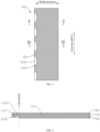


Classifications
-
- H—ELECTRICITY
- H01—ELECTRIC ELEMENTS
- H01M—PROCESSES OR MEANS, e.g. BATTERIES, FOR THE DIRECT CONVERSION OF CHEMICAL ENERGY INTO ELECTRICAL ENERGY
- H01M4/00—Electrodes
- H01M4/02—Electrodes composed of, or comprising, active material
- H01M4/64—Carriers or collectors
- H01M4/66—Selection of materials
- H01M4/665—Composites
- H01M4/667—Composites in the form of layers, e.g. coatings
-
- H—ELECTRICITY
- H01—ELECTRIC ELEMENTS
- H01M—PROCESSES OR MEANS, e.g. BATTERIES, FOR THE DIRECT CONVERSION OF CHEMICAL ENERGY INTO ELECTRICAL ENERGY
- H01M4/00—Electrodes
- H01M4/02—Electrodes composed of, or comprising, active material
- H01M4/04—Processes of manufacture in general
-
- H—ELECTRICITY
- H01—ELECTRIC ELEMENTS
- H01M—PROCESSES OR MEANS, e.g. BATTERIES, FOR THE DIRECT CONVERSION OF CHEMICAL ENERGY INTO ELECTRICAL ENERGY
- H01M4/00—Electrodes
- H01M4/02—Electrodes composed of, or comprising, active material
- H01M4/13—Electrodes for accumulators with non-aqueous electrolyte, e.g. for lithium-accumulators; Processes of manufacture thereof
-
- H—ELECTRICITY
- H01—ELECTRIC ELEMENTS
- H01M—PROCESSES OR MEANS, e.g. BATTERIES, FOR THE DIRECT CONVERSION OF CHEMICAL ENERGY INTO ELECTRICAL ENERGY
- H01M4/00—Electrodes
- H01M4/02—Electrodes composed of, or comprising, active material
- H01M4/13—Electrodes for accumulators with non-aqueous electrolyte, e.g. for lithium-accumulators; Processes of manufacture thereof
- H01M4/134—Electrodes based on metals, Si or alloys
-
- H—ELECTRICITY
- H01—ELECTRIC ELEMENTS
- H01M—PROCESSES OR MEANS, e.g. BATTERIES, FOR THE DIRECT CONVERSION OF CHEMICAL ENERGY INTO ELECTRICAL ENERGY
- H01M4/00—Electrodes
- H01M4/02—Electrodes composed of, or comprising, active material
- H01M4/64—Carriers or collectors
- H01M4/66—Selection of materials
- H01M4/661—Metal or alloys, e.g. alloy coatings
-
- H—ELECTRICITY
- H01—ELECTRIC ELEMENTS
- H01M—PROCESSES OR MEANS, e.g. BATTERIES, FOR THE DIRECT CONVERSION OF CHEMICAL ENERGY INTO ELECTRICAL ENERGY
- H01M4/00—Electrodes
- H01M4/02—Electrodes composed of, or comprising, active material
- H01M4/64—Carriers or collectors
- H01M4/70—Carriers or collectors characterised by shape or form
-
- H—ELECTRICITY
- H01—ELECTRIC ELEMENTS
- H01M—PROCESSES OR MEANS, e.g. BATTERIES, FOR THE DIRECT CONVERSION OF CHEMICAL ENERGY INTO ELECTRICAL ENERGY
- H01M50/00—Constructional details or processes of manufacture of the non-active parts of electrochemical cells other than fuel cells, e.g. hybrid cells
- H01M50/50—Current conducting connections for cells or batteries
- H01M50/531—Electrode connections inside a battery casing
- H01M50/536—Electrode connections inside a battery casing characterised by the method of fixing the leads to the electrodes, e.g. by welding
-
- H—ELECTRICITY
- H01—ELECTRIC ELEMENTS
- H01M—PROCESSES OR MEANS, e.g. BATTERIES, FOR THE DIRECT CONVERSION OF CHEMICAL ENERGY INTO ELECTRICAL ENERGY
- H01M50/00—Constructional details or processes of manufacture of the non-active parts of electrochemical cells other than fuel cells, e.g. hybrid cells
- H01M50/50—Current conducting connections for cells or batteries
- H01M50/531—Electrode connections inside a battery casing
- H01M50/538—Connection of several leads or tabs of wound or folded electrode stacks
-
- H—ELECTRICITY
- H01—ELECTRIC ELEMENTS
- H01M—PROCESSES OR MEANS, e.g. BATTERIES, FOR THE DIRECT CONVERSION OF CHEMICAL ENERGY INTO ELECTRICAL ENERGY
- H01M4/00—Electrodes
- H01M4/02—Electrodes composed of, or comprising, active material
- H01M2004/026—Electrodes composed of, or comprising, active material characterised by the polarity
- H01M2004/027—Negative electrodes
-
- H—ELECTRICITY
- H01—ELECTRIC ELEMENTS
- H01M—PROCESSES OR MEANS, e.g. BATTERIES, FOR THE DIRECT CONVERSION OF CHEMICAL ENERGY INTO ELECTRICAL ENERGY
- H01M4/00—Electrodes
- H01M4/02—Electrodes composed of, or comprising, active material
- H01M2004/026—Electrodes composed of, or comprising, active material characterised by the polarity
- H01M2004/028—Positive electrodes
-
- H—ELECTRICITY
- H01—ELECTRIC ELEMENTS
- H01M—PROCESSES OR MEANS, e.g. BATTERIES, FOR THE DIRECT CONVERSION OF CHEMICAL ENERGY INTO ELECTRICAL ENERGY
- H01M4/00—Electrodes
- H01M4/02—Electrodes composed of, or comprising, active material
- H01M2004/026—Electrodes composed of, or comprising, active material characterised by the polarity
- H01M2004/029—Bipolar electrodes
-
- H—ELECTRICITY
- H01—ELECTRIC ELEMENTS
- H01M—PROCESSES OR MEANS, e.g. BATTERIES, FOR THE DIRECT CONVERSION OF CHEMICAL ENERGY INTO ELECTRICAL ENERGY
- H01M4/00—Electrodes
- H01M4/02—Electrodes composed of, or comprising, active material
- H01M4/04—Processes of manufacture in general
- H01M4/0402—Methods of deposition of the material
- H01M4/0404—Methods of deposition of the material by coating on electrode collectors
-
- Y—GENERAL TAGGING OF NEW TECHNOLOGICAL DEVELOPMENTS; GENERAL TAGGING OF CROSS-SECTIONAL TECHNOLOGIES SPANNING OVER SEVERAL SECTIONS OF THE IPC; TECHNICAL SUBJECTS COVERED BY FORMER USPC CROSS-REFERENCE ART COLLECTIONS [XRACs] AND DIGESTS
- Y02—TECHNOLOGIES OR APPLICATIONS FOR MITIGATION OR ADAPTATION AGAINST CLIMATE CHANGE
- Y02E—REDUCTION OF GREENHOUSE GAS [GHG] EMISSIONS, RELATED TO ENERGY GENERATION, TRANSMISSION OR DISTRIBUTION
- Y02E60/00—Enabling technologies; Technologies with a potential or indirect contribution to GHG emissions mitigation
- Y02E60/10—Energy storage using batteries
-
- Y—GENERAL TAGGING OF NEW TECHNOLOGICAL DEVELOPMENTS; GENERAL TAGGING OF CROSS-SECTIONAL TECHNOLOGIES SPANNING OVER SEVERAL SECTIONS OF THE IPC; TECHNICAL SUBJECTS COVERED BY FORMER USPC CROSS-REFERENCE ART COLLECTIONS [XRACs] AND DIGESTS
- Y02—TECHNOLOGIES OR APPLICATIONS FOR MITIGATION OR ADAPTATION AGAINST CLIMATE CHANGE
- Y02P—CLIMATE CHANGE MITIGATION TECHNOLOGIES IN THE PRODUCTION OR PROCESSING OF GOODS
- Y02P70/00—Climate change mitigation technologies in the production process for final industrial or consumer products
- Y02P70/50—Manufacturing or production processes characterised by the final manufactured product
Definitions
- the present disclosure relates to the technical field of secondary batteries, and in particular, to a bipolar current collector, an electrode sheet, a battery cell, and a secondary battery.
- a negative electrode current collector is a polymer layer coated with copper metal layers on both sides of the polymer layer
- a positive electrode current collector is usually a polymer layer coated with aluminum metal layers on both sides thereof the polymer layer.
- the composite current collector is used to prepare an electrode sheet and a secondary battery.
- a bipolar current collector in which a copper layer and an aluminum layer are respectively formed on the two surfaces of an insulation film layer.
- the copper layer serves as a negative electrode
- the aluminum layer serves as a positive electrode to prepare an electrode sheet and a secondary battery.
- the insulation film layer may be easily penetrated by the welding, and thus the copper layer and the aluminum layer are in contact, thereby resulting in the problem of short circuit between the positive and negative electrodes.
- the present disclosure aims to provide a bipolar current collector, an electrode sheet, a battery cell, and a secondary battery, capable of alleviating the problem of short circuit between positive and negative electrodes to a certain extent.
- the present disclosure provides a bipolar current collector.
- the bipolar current collector includes an insulation film layer, a positive electrode metal layer, and a negative electrode metal layer.
- the insulation film layer has a first surface and a second surface in a thickness direction.
- the positive electrode metal layer is disposed on one of the first surface and the second surface, and the negative electrode metal layer is disposed on the other one of the first surface and the second surface.
- the insulation film layer has a first region portion configured to be connected to a tab.
- the first surface located at the first region portion has a first exposed region and a first metal region
- the second surface located at the first region portion has a second exposed region and a second metal region.
- the positive electrode metal layer is disposed in one of the first metal region and the second metal region
- the negative electrode metal layer is disposed in the other one of the first metal region and the second metal region.
- a projection of the first metal region on a reference plane does not exceed a projection of the second exposed region on the reference plane.
- a projection of the second metal region on the reference plane does not exceed a projection of the first exposed region on the reference plane.
- the reference plane is a symmetry surface of the insulation film layer in the thickness direction.
- the symmetry surface of the insulation film layer in the thickness direction is used as the reference plane; the projection of the first metal region on the reference plane does not exceed the projection of the second exposed region on the reference plane; and the projection of the second metal region on the reference plane does not exceed the projection of the first exposed region on the reference plane.
- an area of the projection of the first metal region on the reference plane is smaller than an area of the projection of the corresponding second exposed region on the reference plane, and an area of the projection of the second metal region on the reference plane is smaller than an area of the projection of the corresponding first exposed region on the reference plane.
- a plurality of first exposed regions and a plurality of first metal regions are provided and alternately arranged in the length direction of the bipolar current collector; a plurality of second exposed regions and a plurality of second metal regions are provided and alternately arranged in the length direction of the bipolar current collector.
- the metal layers on the two surfaces of the first region portion are used to connect the tabs.
- the positive electrode metal layer, the first exposed region, the positive electrode metal layer and the first exposed region are alternately arranged.
- the second exposed region, the negative electrode metal layer, the second exposed region, and the negative electrode metal layer are alternately arranged.
- the metal regions on the two surfaces are arranged in a one-to-one correspondence with the exposed regions.
- the damaged part of the insulation film layer only has a positive electrode metal layer on one side, and has no metal layer on the other side, as the backside of the positive electrode metal layer is the second exposed region. Therefore, the positive electrode metal layer and the negative electrode metal layer respectively disposed on two surfaces of the insulation film layer will not be in contact and in conduction, even when the insulation film layer is damaged, thereby avoiding the problem of the short circuit between the positive and negative electrodes to a certain extent.
- the damaged part of the insulation film layer only has a negative electrode metal layer on one side, and has no metal layer on the other side, as the backside of the negative electrode metal layer is the first exposed region. Therefore, the positive electrode metal layer and the negative electrode metal layer respectively disposed on both surfaces of the insulation film layer will not be in contact and in conduction, even when the insulation film layer is damaged, thereby avoiding the problem of the short circuit between the positive and negative electrodes to a certain extent.
- a projection, on the reference plane, of an end of each first metal region close to an adjacent second metal region is spaced apart from a projection, on the reference plane, of an end of the adjacent second metal region close to the corresponding first metal region by a predetermined distance.
- a width of each of the plurality of first metal regions is smaller than a width of the corresponding second exposed region, and a width of each of the plurality of second metal regions is smaller than a width of the corresponding first exposed region.
- the first metal region exactly corresponds to the second exposed region, during connecting (for example, welding) the positive electrode tab on the positive electrode metal layer on the first metal region, a welding mark may also exist at the periphery of the positive electrode metal layer on the first metal region, and thus it may result in that the insulation film layer is penetrated by the welding thereby avoiding the contact between the positive electrode metal layer on the first metal region and the negative electrode metal layer on the second metal region, which may result in a short circuit between the positive and negative electrodes. Therefore, the above limitations of the width may greatly reduce the occurrence of this problem.
- the second metal region exactly corresponds to the first exposed region, during connecting (for example, welding) the negative electrode tab on the negative electrode metal layer on the second metal region, a welding mark may also exist at the periphery of the negative electrode metal layer on the second metal region, and thus it may result in that the insulation film layer is penetrated by the welding.
- the negative electrode metal layer on the second metal region may come into contact with the positive electrode metal layer on the first metal region, resulting in a short circuit between the positive and negative electrodes. Therefore, the above limitation of the width may greatly reduce the occurrence of this problem.
- two sides of the second exposed region exceed two sides of a projection of the corresponding first metal region on the second exposed region, respectively, and two sides of the first exposed region exceed two sides of a projection of the corresponding second metal region on the first exposed region, respectively.
- the projection of the first metal region on the second exposed region is entirely located within the second exposed region, and the exposed region is relatively large. Even if the welding marks exist around the periphery of the positive electrode metal layer on the first metal region, the positive electrode metal layer and the negative electrode metal layer can be effectively prevented from being in contact with each other, thereby avoiding the short circuit between the positive and negative electrodes.
- the projection of the second metal region on the first exposed region is entirely located within the first exposed region, and the exposed region is relatively large. Even if the welding marks exist around the periphery of the negative electrode metal layer on the second metal region, the positive electrode metal layer and the negative electrode metal layer can be effectively prevented from being in contact with each other, thereby avoiding the short circuit between the positive and negative electrodes.
- a difference between the width of the second exposed region and the width of the first metal region ranges from 2 mm to 20 mm, and a difference between the width of the first exposed region and the width of the second metal region ranges from 2 mm to 20 mm.
- the width difference can effectively avoid the short circuit between the positive and negative electrodes and can also ensure the area of the metal layers in the tab region, facilitating the connection of the tabs.
- the insulation film layer further has a second region portion, and wherein the second region portion and the first region portion are sequentially arranged in a width direction of the bipolar current collector.
- the first metal region is coated with the positive electrode metal layer to be connected a positive electrode tab, and the second metal region is coated with the negative electrode metal layer to connect a negative electrode tab; and the first surface located at the second region portion is entirely coated with the positive electrode metal layer, and the second surface located at the second region portion is entirely coated with the negative electrode metal layer.
- the positive electrode metal layer is an aluminum metal layer
- the negative electrode metal layer is a copper metal layer or a nickel metal layer.
- the aluminum metal layer is used as the positive electrode of the bipolar current collector and the copper metal layer or the nickel metal layer is used as the negative electrode of the bipolar current collector, the current conduction and confluence ability of the positive and negative electrodes can be improved and easily obtained.
- the present disclosure provides an electrode sheet.
- the electrode sheet includes: the above bipolar current collector; a positive electrode active material layer disposed on the positive electrode metal layer on a second region of the insulation film layer; a negative electrode active material layer disposed on the negative electrode metal layer on the second region of the insulation film layer; a positive electrode tab disposed on the positive electrode metal layer on the first metal region; and a negative electrode tab disposed on the negative electrode metal layer on the second metal region.
- the electrode sheet prepared by using the above bipolar current collector may effectively avoid the short circuit between the positive and negative electrodes when connecting the tabs.
- the present disclosure provides a battery cell.
- the battery cell includes a plurality of electrode sheets as described above, and a plurality of separators. Each of the plurality of separators is disposed between two adjacent electrode sheets of the plurality of electrode sheets.
- the positive electrode active material layer and the negative electrode active material layer are respectively arranged on two sides of each of the plurality of separators.
- the battery cell is a laminated battery cell stack, wherein each of the plurality of electrode sheets comprises a positive electrode tab and a negative electrode tab; and when the plurality of electrode sheets is stacked, the positive electrode tabs of the plurality of electrode sheets overlap, and the negative electrode tabs of the plurality of electrode sheets overlap.
- the cell stack can be used to prepare a laminated battery.
- the positive electrode tabs and the negative electrode tabs on the same side are arranged at intervals.
- the positive electrode tabs overlap, and the overlapped positive electrode tabs are connected to the positive electrode connecting piece;
- the negative electrode tabs overlap, and the overlapped negative electrode tabs are connected to the negative electrode connecting piece, thereby obtaining a laminated battery having a simple structure.
- the battery cell is a wound battery cell, in a winding direction of the plurality of electrode sheets, a distance between two adjacent positive electrode tabs and a distance between two adjacent two negative electrode tabs are gradually increased in such a manner that, when the plurality of electrode sheets and the plurality of separators are wound, the positive electrode tabs overlap, and the negative electrode tabs overlap.
- the present disclosure provides a secondary battery.
- the secondary battery includes the above battery cell.
- the electrical performance of the secondary battery is better.
- 100 - bipolar current collector 110 - insulation film layer; 120 - positive electrode metal layer; 130 - negative electrode metal layer; 111 - first region portion; 112 - second region portion; 1213 - first metal region; 1214 - first exposed region; 1215 - second metal region; 1216 - second exposed region; 200 - electrode sheet; 210 - positive electrode active material layer; 220 - negative electrode active material layer; 230 - positive electrode tab; 240 - negative electrode tab.
- first and second are only for descriptive purposes, and they cannot be understood as indicating or implying relative importance or implicitly indicating the number of indicated technical features. Therefore, the features defined with “first” or “second” may explicitly or implicitly include at least one of the features. In the description of the present disclosure, “plurality” means at least two, for example, two, three, etc., unless otherwise specifically defined.
- a bipolar current collector 100 includes an insulation film layer 110, a positive electrode metal layer 120, and a negative electrode metal layer 130.
- the insulation film layer 110 has a first surface and a second surface in a thickness direction.
- the positive electrode metal layer 120 is disposed on one of the first surface and the second surface, and the negative electrode metal layer 130 is disposed on the other one of the first surface and the second surface.
- the positive electrode metal layer 120 may be disposed on the first surface, and the negative electrode metal layer 130 may be disposed on the second surface; or the negative electrode metal layer 130 may be disposed on the first surface, and the positive electrode metal layer 120 may be disposed on the second surface.
- the insulation film layer 110 has a first region portion 111 configured to be connected to a tab.
- the first surface located at the first region portion 111 has a first exposed region 1214 and a first metal region 1213; the second surface located at the first region portion 111 has a second exposed region 1216 and a second metal region 1215.
- the positive electrode metal layer 120 is disposed in one of the first metal region 1213 and the second metal region 1215; and the negative electrode metal layer 130 is disposed in the other one of the first metal region 1213 and the second metal region 1215.
- the positive electrode metal layer 120 is disposed in the first metal region 1213, and the negative electrode metal layer 130 is disposed in the second metal region 1215; or the negative electrode metal layer 130 is disposed in the first metal region 1213, and the positive electrode metal layer 120 is disposed in the second metal region 1215.
- a projection of the first metal region 1213 on a reference plane does not exceed a projection of the second exposed region 1216 on the reference plane, and a projection of the second metal region 1215 on the reference plane does not exceed a projection of the first exposed region 1214 on the reference plane.
- the reference plane is a symmetry surface of the insulation film layer 110 in the thickness direction. For example, taking the symmetry surface of the insulation film layer 110 in the thickness direction as the reference plane, the projection of the first metal region 1213 on the reference plane does not exceed the projection of the second exposed region 1216 on the reference plane, and the projection of the second metal region 1215 on the reference plane does not exceed the projection of the first exposed region 1214 on the reference plane.
- the symmetry surface of the insulation film layer 110 in the thickness direction is used as the reference plane; the projection of the first metal region 1213 on the reference plane does not exceed the projection of the second exposed region 1216 on the reference plane; and the projection of the second metal region 1215 on the reference plane does not exceed the projection of the first exposed region 1214 on the reference plane.
- an area of the projection of the first metal region 1213 on the reference plane is smaller than an area of the projection of the corresponding second exposed region 1216 on the reference plane; and an area of the projection of the second metal region 1215 on the reference plane is smaller than an area of the projection of the corresponding first exposed region 1214 on the reference plane.
- the projection has a rectangle form, and a set is taken as an example for description.
- the projection region of the first metal region 1213 on the reference plane includes the corresponding projection region of the second exposed region 1216 on the reference plane; and the projection region of the second metal region 1215 on the reference plane includes the corresponding projection region of the first exposed region 1214 on the reference plane.
- the projection of the first metal region 1213 on the reference plane is located within the projection of the second exposed region 1216 on the reference plane; and the projection of the second metal region 1215 on the reference plane is located within the projection of the first exposed region 1214 on the reference plane.
- the positive electrode metal layer 120 and the negative electrode metal layer 130 on both surfaces of the insulation film layer 110 are in contact and in conduction, so as to avoid the problem of the short circuit between the positive and negative electrodes to a certain extent.
- a projection of an end of the first metal region 1213 close to an adjacent second metal region 1215 is spaced apart from a projection of an end of the adjacent second metal region 1215 close to the corresponding first metal region 1213 by a predetermined distance, which is conducive to avoiding the short circuit between the positive and negative electrodes
- the insulation film layer 110 further has a second region portion 112.
- the second region portion 112 and the first region portion 111 are sequentially arranged in a width direction of the bipolar current collector 100.
- the first metal region 1213 is coated with the positive electrode metal layer 120 to connect a positive electrode tab 230
- the second metal region 1215 is coated with the negative electrode metal layer 130 to connect a negative electrode tab 240.
- the first surface located at the second region portion 112 is entirely coated with the positive electrode metal layer 120
- the second surface located at the second region portion 112 is entirely coated with the negative electrode metal layer 130.
- a plurality of first exposed regions 1214 and a plurality of first metal regions 1213 are provided.
- the plurality of first exposed regions 1214 and the plurality of first metal regions 1213 are alternately arranged in the length direction of the bipolar current collector 100.
- a plurality of second exposed regions 1216 and a plurality of second metal regions 1215 are provided.
- the plurality of second exposed regions 1216 and the plurality of second metal regions 1215 are alternately arranged in the length direction of the bipolar current collector 100.
- the metal layers on the two surfaces of the first region portion 111 are used to connect the tabs.
- the positive electrode metal layer 120, the first exposed region 1214, the positive electrode metal layer 120, and the first exposed regions 1214 are alternately arranged; and on the second surface located at the first region portion 111, the second exposed region 1216, the negative electrode metal layer 130, the second exposed region 1216, and the negative electrode metal layer 130 are alternately arranged.
- the metal regions and the exposed regions on one on the two surfaces are arranged in a one-to-one correspondence.
- the damaged part of the insulation film layer 110 only has the positive electrode metal layer 120 on one side, and has no metal layer on the other side, as the backside of the positive electrode metal layer 120 is the second exposed region 1216. Therefore, the positive electrode metal layer 120 and the negative electrode metal layer 130 respectively disposed on two surfaces of the insulation film layer 110 will not be in contact and in conduction, even when the insulation film layer 110 is damaged, thereby avoiding the problem of the short circuit between the positive and negative electrodes to a certain extent.
- the damaged part of the insulation film layer 110 only has the negative electrode metal layer 130 on one side, and has no metal layer on the other side, as the backside of the negative electrode metal layer 130 is an exposed region 1214. Therefore, the positive electrode metal layer 120 and the negative electrode metal layer 130 respectively disposed on two surfaces of the insulation film layer 110 will not be in contact and in conduction, even when the insulation film layer 110 is damaged, thereby avoiding the problem of the short circuit between the positive and negative electrodes to a certain extent.
- FIG. 1 is a structural schematic diagram of a bipolar current collector 100 according to an embodiment of the present disclosure
- FIG. 2 is a sectional view along II to II in FIG. 1
- FIG. 3 is a sectional view along III to III in FIG. 1 .
- the bipolar current collector 100 in a thickness direction of the bipolar current collector 100, includes an insulation film layer 110, a positive electrode metal layer 120, and a negative electrode metal layer 130 disposed on both surfaces of the insulation film layer 110.
- the insulation film layer 110 In a width direction of the bipolar current collector 100, has a first region portion 111 and a second region portion 112 arranged in sequence.
- the first region portion 111 is located on one side of the second region portion 112. As illustrated in FIG. 2 and FIG. 3 , the region on the left side of dotted line 1 and dotted line 2 is the first region portions 111, and region on the right side of dotted line 1 and dotted line 2 is the second region portions 112.
- the material of the insulation film layer 110 may be a polymer insulation layer, for example, a film layer made of polystyrene, polypropylene, polyester, polycarbonate, polytetrafluoroethylene, polyimide; the material of the insulation film layer 110 may also be synthetic fiber insulating paper, for example, aramid fiber paper, polyester fiber paper; or the material of the insulation film layer 110 may be various insulation tapes, and the like.
- a polymer insulation layer for example, a film layer made of polystyrene, polypropylene, polyester, polycarbonate, polytetrafluoroethylene, polyimide
- the material of the insulation film layer 110 may also be synthetic fiber insulating paper, for example, aramid fiber paper, polyester fiber paper
- the material of the insulation film layer 110 may be various insulation tapes, and the like.
- first exposed regions 1214, and first metal regions 1213 covered by the positive electrode metal layer 120 are alternatively arranged on the first surface located at the first region portion 111; second exposed regions 1216, and second metal regions 1215 covered by the negative electrode metal layer 130 are alternatively arranged on the second surface located at the first region portion 111.
- the positive electrode metal layer 120 is formed on the first surface located at the second region portion 112, and the negative electrode metal layer 130 is formed on the second surface of the second region portion 112.
- the positive electrode metal layer 120 is an aluminum metal layer
- the negative electrode metal layer 130 is a copper metal layer or a nickel metal layer.
- the positive electrode metal layer 120 is an aluminum metal layer for conducting the positive current
- the negative electrode metal layer 130 is a copper metal layer for conducting the negative current.
- the positive electrode metal layer 120 is not limited to an aluminum metal layer, as long as the positive electrode metal layer serving as the current collector is within the scope of protection of the present disclosure
- the negative electrode metal layer 130 is not limited to a copper metal layer, as long as the negative electrode metal layer serving as the current collector is within the scope of protection of the present disclosure.
- a thickness of the positive electrode metal layer 120 ranges from 20 nm to 1500 nm
- a thickness of the negative electrode metal layer 130 ranges from 30 nm to 2500 nm.
- the layer structure with the above thickness can ensure the over-current capability, and thus the current collector has better electrical conductivity.
- the thickness of the positive electrode metal layer 120 is 20 nm, 100 nm, 500 nm, 800 nm, 1000 nm, or 1500 nm
- the thickness of the negative electrode metal layer 130 is 30 nm, 200 nm, 600 nm, 900 nm, 1500 nm, 2000 nm, or 2500 nm.
- a positive electrode metal layer 120 may be deposited on one surface of the insulation film layer 110; and a negative electrode metal layer 130 may be deposited on the other surface of the insulation film layer 110.
- One side of the bipolar current collector 100 is selected as a tab region. At the tab region, a part of the positive electrode metal layer 120 and a part of the negative electrode metal layer 130 may be removed to form a first exposed region 1214 and a second exposed region 1216, thereby obtaining the structure of the bipolar current collector 100 as illustrated in FIG. 1 .
- FIG. 4 is a structural schematic diagram of an electrode sheet 200 according to an embodiment of the present disclosure
- FIG. 5 is a sectional view along V to V in FIG. 4
- FIG. 6 is a sectional view along VI to VI in FIG. 4 .
- an electrode sheet 200 includes the above-described bipolar current collector 100, a positive electrode active material layer 210, a negative electrode active material layer 220, and positive electrode tabs 230, and negative electrode tabs 240.
- the positive electrode active material layer 210 is disposed on the positive electrode metal layer 120 of the second region portion 112 of the insulation film layer, and the negative electrode active material layer 220 is disposed on the negative electrode metal layer 130 of the second region portion 112 of the insulation film layer.
- One positive electrode tab 230 is disposed on the positive electrode metal layer 120 on one of the first metal regions 1213, and one negative electrode tab 240 is disposed on the negative electrode metal layer 130 on one second metal region 1215.
- the positive electrode tab 230 is welded to the positive electrode metal layer 120, and the negative electrode tab 240 is welded to the negative electrode metal layer 130.
- the tabs are connected by welding, the connection between the tabs and the metal layers can be more robust.
- the problem of welding-penetration of the insulation film layer 110 is likely to occur.
- a projection of the first metal region 1213 in the thickness direction of the insulation film layer 110 does not exceed the second exposed region 1216.
- the upper surface of the insulation film layer 110 is the positive electrode metal layer 120
- the lower surface of the insulation film layer 110 is the second exposed region 1216.
- the positive electrode metal layer 120 and the negative electrode metal layer 130 respectively disposed on two surfaces of the insulation film layer 110 will not be in contact and in conduction, even when the insulation film layer 110 is damaged, thereby avoiding the problem of the short circuit between the positive and negative electrodes to a certain extent.
- the projection of the second metal region 1215 in the thickness direction of the insulation film layer 110 does not exceed the first exposed region 1214.
- the lower surface of the insulation film layer 110 is the negative electrode metal layer 130
- the upper surface of the insulation film layer 110 is the first exposed region 1214.
- the positive electrode metal layer 120 and the negative electrode metal layer 130 respectively disposed on two surfaces of the insulation film layer 110 will not be in contact and in conduction, even when the insulation film layer 110 is damaged, thereby avoiding the problem of the short circuit between the positive and negative electrodes to a certain extent.
- a shape of the first metal region 1213 corresponds to a shape of the second exposed region 1216; a shape of the second metal region 1215 corresponds to a shape of the first exposed region 1214; the projection of the first metal region 1213 in the thickness direction of the insulation film layer 110 overlaps the second exposed region 1216; and the projection of the second metal region 1215 in the thickness direction of the insulation film layer 110 overlaps the first exposed region 1214.
- a welding mark may also exist at the periphery of the positive electrode metal layer 120 in the first metal region 1213, and thus it may result in that the insulation film layer 110 is penetrated by the welding, thereby avoiding the contact between the positive electrode metal layer 120 in the first metal region 1213 and the negative electrode metal layer 130 in the second metal region 1215, which may result in a short circuit between the positive electrode and the negative electrode. Therefore, in another embodiment of the present disclosure, further referring to FIG. 1 and FIG.
- the first metal region 1213 has a smaller width than the corresponding second exposed region 1216, and the second metal region 1215 has a smaller width than the corresponding first exposed region 1214.
- the above limitations of the width can greatly reduce the occurrence of the above-mentioned problem. Even if the insulation film layer 110 corresponding to the edge of the first metal layer is penetrated by the welding, the conduction between the positive and negative electrodes may be effectively avoided, as the corresponding exposed region is wider.
- two sides of the second exposed region 1216 exceed two sides of a projection of the corresponding first metal region 1213 on the second exposed region 1216, respectively, and two sides of the first exposed region 1214 exceed two sides of a projection of the corresponding second metal region 1215 on the first exposed region 1214, respectively.
- the dotted region is the second metal region 1215.
- the area of the first metal region 1213 is smaller than the area of the second exposed region 1216, and the first metal region 1213 is entirely located within the second exposed region 1216; the area of the second metal region 1215 is smaller than the area of the first exposed region 1214, and the second metal region 1215 is entirely located within the first exposed region 1214.
- the contact between the positive electrode metal layer 120 and the negative electrode metal layer 130 can be effectively avoided during the welding of tabs, thereby avoiding the short circuit between the positive electrode and the negative electrode.
- a difference between the width of the second exposed region 1216 and width of the first metal region 1213 ranges from 2 mm to 20 mm; and a difference between the width of the first exposed region 1214 and the width of the second metal region 1215 ranges from 2 mm to 20 mm.
- the width difference can effectively avoid the short circuit between the positive and negative electrodes and can also ensure the area of the metal layer on the tab region, for connecting the tabs.
- the difference between the width of the second exposed region 1216 and the width of the first metal region 1213 is 2 mm, 8 mm, 15 mm, or 20 mm, etc.; and the difference between the width of the first exposed region 1214 and the width of the second metal region 1215 is 2 mm, 8 mm, 15 mm, or 20 mm, etc.
- one side of the projection of the first metal layer on the thickness direction of the insulation film layer 110 may correspond to the edge of the second exposed region 1216, and the other side may be located within the second exposed region 1216; one side of the projection of the second metal region 1215 in the thickness direction of the insulation film layer 110 corresponds to the edge of the first exposed region 1214, and the other side is located within the first exposed region 1214, which is not limited in the present disclosure.
- FIG. 7 is a schematic diagram of a second structure of an electrode sheet 200 according to an embodiment of the present disclosure.
- both the positive electrode tab 230 and the negative electrode tab 240 has substantially a trapezoid structure. That is, along the length direction of the bipolar current collector 100, the width of a side of the tab close to the coating region is greater, while the width of a side of the tab facing away from the coating region is smaller. In this way, a welding area between the tab and the metal layer is relatively larger, allowing the welding between the tab and the metal layer to be firmer.
- a welding area between the tab and the connecting piece is relatively smaller, the number of tabs can be reduced and the energy density of the battery can be increased, while ensuring the welding firmness.
- the shapes of the first metal region 1213 and the second metal region 1215 correspond to the shapes of the positive electrode tab 230 and the negative electrode tab 240, respectively. Therefore, the positive electrode tab 230 can be connected to the positive electrode metal layer 120 in the first metal region 1213, and the negative electrode tab 240 can be connected to the negative electrode metal layer 130 in the second metal region 1215.
- the above electrode sheet 200 may be used in a secondary battery.
- the secondary battery may be a laminated battery, a wound battery, or the like, which is not limited in the present disclosure.
- a battery cell is first manufactured using the electrode sheet 200, and the secondary battery is then manufactured using the battery cell.
- the battery cell includes a plurality of the electrode sheets 200 as described above, and a plurality of separators.
- One separator is disposed between two adjacent electrode sheets 200.
- the positive electrode active material layer 210 and the negative electrode active material layer 220 are respectively arranged on two sides of the separators.
- FIG. 8 is a structural schematic diagram of a battery electrode sheet 200 in a battery cell stack according to an embodiment of the present disclosure.
- the battery cell is a laminated battery cell stack.
- Each electrode sheet 200 includes a positive electrode tab 230 and a negative electrode tab 240.
- the positive electrode tabs 230 of the plurality of electrode sheets 200 overlap, and the negative electrode tabs 240 of the plurality of electrode sheets 200 overlap.
- the overlapping positive electrode tabs 230 are welded to a positive electrode connecting piece, and the overlapping negative electrode tabs 240 are connected to the negative electrode connecting piece, for manufacturing a secondary battery.
- the battery cell is a wound battery cell.
- a distance between two adjacent positive electrode tabs 230 and a distance between two adjacent negative electrode tabs 240 are gradually increased. That is, a diameter of an inner ring of the wound battery cell is small, and a diameter of an outer ring is great, such that it is necessary to set different tab distances.
- the overlapping positive electrode tabs 230 are welded to a positive electrode connecting piece, and the overlapping negative electrode tabs 240 are connected to a negative electrode connecting piece, for manufacturing a secondary battery.
- the bipolar current collector 100 and the electrode sheet 200 according to the embodiments of the present disclosure have the following beneficial effects.
Landscapes
- Chemical & Material Sciences (AREA)
- Chemical Kinetics & Catalysis (AREA)
- Electrochemistry (AREA)
- General Chemical & Material Sciences (AREA)
- Engineering & Computer Science (AREA)
- Materials Engineering (AREA)
- Composite Materials (AREA)
- Manufacturing & Machinery (AREA)
- Connection Of Batteries Or Terminals (AREA)
- Secondary Cells (AREA)
Abstract
Description
- This application is based on and claims the priority of the
Chinese Patent Application No. 202021523469.0, filed on July 28, 2020 - The present disclosure relates to the technical field of secondary batteries, and in particular, to a bipolar current collector, an electrode sheet, a battery cell, and a secondary battery.
- In a composite current collector, a negative electrode current collector is a polymer layer coated with copper metal layers on both sides of the polymer layer, and a positive electrode current collector is usually a polymer layer coated with aluminum metal layers on both sides thereof the polymer layer. The composite current collector is used to prepare an electrode sheet and a secondary battery.
- In order to further improve an energy density of a battery, in the related art, a bipolar current collector is provided, in which a copper layer and an aluminum layer are respectively formed on the two surfaces of an insulation film layer. The copper layer serves as a negative electrode, and the aluminum layer serves as a positive electrode to prepare an electrode sheet and a secondary battery. However, in the process of tab welding, the insulation film layer may be easily penetrated by the welding, and thus the copper layer and the aluminum layer are in contact, thereby resulting in the problem of short circuit between the positive and negative electrodes.
- The present disclosure aims to provide a bipolar current collector, an electrode sheet, a battery cell, and a secondary battery, capable of alleviating the problem of short circuit between positive and negative electrodes to a certain extent. In a first aspect, the present disclosure provides a bipolar current collector. The bipolar current collector includes an insulation film layer, a positive electrode metal layer, and a negative electrode metal layer. The insulation film layer has a first surface and a second surface in a thickness direction. The positive electrode metal layer is disposed on one of the first surface and the second surface, and the negative electrode metal layer is disposed on the other one of the first surface and the second surface. The insulation film layer has a first region portion configured to be connected to a tab. In a length direction of the bipolar current collector, the first surface located at the first region portion has a first exposed region and a first metal region, and the second surface located at the first region portion has a second exposed region and a second metal region. The positive electrode metal layer is disposed in one of the first metal region and the second metal region, and the negative electrode metal layer is disposed in the other one of the first metal region and the second metal region. A projection of the first metal region on a reference plane does not exceed a projection of the second exposed region on the reference plane. A projection of the second metal region on the reference plane does not exceed a projection of the first exposed region on the reference plane. The reference plane is a symmetry surface of the insulation film layer in the thickness direction.
- In the bipolar current collector according to the embodiments of the present disclosure, the symmetry surface of the insulation film layer in the thickness direction is used as the reference plane; the projection of the first metal region on the reference plane does not exceed the projection of the second exposed region on the reference plane; and the projection of the second metal region on the reference plane does not exceed the projection of the first exposed region on the reference plane. In this way, when the first metal region or the second metal region is connected to the corresponding tab, due to the presence of the exposed region on the surface of the insulation film layer opposite to the first metal region or the second metal region, it can be avoided that the positive electrode metal layer and the negative electrode metal layer on both surfaces of the insulation film layer are in contact and in conduction, so as to avoid the problem of the short circuit between the positive and negative electrodes to a certain extent.
- According to some embodiments of the present disclosure, an area of the projection of the first metal region on the reference plane is smaller than an area of the projection of the corresponding second exposed region on the reference plane, and an area of the projection of the second metal region on the reference plane is smaller than an area of the projection of the corresponding first exposed region on the reference plane.
- According to some embodiments of the present disclosure, a plurality of first exposed regions and a plurality of first metal regions are provided and alternately arranged in the length direction of the bipolar current collector; a plurality of second exposed regions and a plurality of second metal regions are provided and alternately arranged in the length direction of the bipolar current collector. The metal layers on the two surfaces of the first region portion are used to connect the tabs. On the first surface located at the first region portion, the positive electrode metal layer, the first exposed region, the positive electrode metal layer and the first exposed region are alternately arranged. On the second surface located at the first region portion, the second exposed region, the negative electrode metal layer, the second exposed region, and the negative electrode metal layer are alternately arranged. At the first region portion, the metal regions on the two surfaces are arranged in a one-to-one correspondence with the exposed regions.
- During connecting the positive electrode tab to the positive electrode metal layer on the first metal region, even if the insulation film layer at the connection position is inevitably damaged, the damaged part of the insulation film layer only has a positive electrode metal layer on one side, and has no metal layer on the other side, as the backside of the positive electrode metal layer is the second exposed region. Therefore, the positive electrode metal layer and the negative electrode metal layer respectively disposed on two surfaces of the insulation film layer will not be in contact and in conduction, even when the insulation film layer is damaged, thereby avoiding the problem of the short circuit between the positive and negative electrodes to a certain extent.
- During connecting the negative electrode tab to the negative electrode metal layer on the first region portion, even if the insulation film layer at the connection position is inevitably damaged, the damaged part of the insulation film layer only has a negative electrode metal layer on one side, and has no metal layer on the other side, as the backside of the negative electrode metal layer is the first exposed region. Therefore, the positive electrode metal layer and the negative electrode metal layer respectively disposed on both surfaces of the insulation film layer will not be in contact and in conduction, even when the insulation film layer is damaged, thereby avoiding the problem of the short circuit between the positive and negative electrodes to a certain extent.
- According to some embodiments of the present disclosure, in the length direction of the bipolar current collector, a projection, on the reference plane, of an end of each first metal region close to an adjacent second metal region is spaced apart from a projection, on the reference plane, of an end of the adjacent second metal region close to the corresponding first metal region by a predetermined distance.
- In a possible implementation manner, along the length direction of the bipolar current collector, a width of each of the plurality of first metal regions is smaller than a width of the corresponding second exposed region, and a width of each of the plurality of second metal regions is smaller than a width of the corresponding first exposed region.
- If the first metal region exactly corresponds to the second exposed region, during connecting (for example, welding) the positive electrode tab on the positive electrode metal layer on the first metal region, a welding mark may also exist at the periphery of the positive electrode metal layer on the first metal region, and thus it may result in that the insulation film layer is penetrated by the welding thereby avoiding the contact between the positive electrode metal layer on the first metal region and the negative electrode metal layer on the second metal region, which may result in a short circuit between the positive and negative electrodes. Therefore, the above limitations of the width may greatly reduce the occurrence of this problem. If the second metal region exactly corresponds to the first exposed region, during connecting (for example, welding) the negative electrode tab on the negative electrode metal layer on the second metal region, a welding mark may also exist at the periphery of the negative electrode metal layer on the second metal region, and thus it may result in that the insulation film layer is penetrated by the welding. Thus, the negative electrode metal layer on the second metal region may come into contact with the positive electrode metal layer on the first metal region, resulting in a short circuit between the positive and negative electrodes. Therefore, the above limitation of the width may greatly reduce the occurrence of this problem.
- In a possible implementation manner, along the length direction of the bipolar current collector, two sides of the second exposed region exceed two sides of a projection of the corresponding first metal region on the second exposed region, respectively, and two sides of the first exposed region exceed two sides of a projection of the corresponding second metal region on the first exposed region, respectively.
- The projection of the first metal region on the second exposed region is entirely located within the second exposed region, and the exposed region is relatively large. Even if the welding marks exist around the periphery of the positive electrode metal layer on the first metal region, the positive electrode metal layer and the negative electrode metal layer can be effectively prevented from being in contact with each other, thereby avoiding the short circuit between the positive and negative electrodes. The projection of the second metal region on the first exposed region is entirely located within the first exposed region, and the exposed region is relatively large. Even if the welding marks exist around the periphery of the negative electrode metal layer on the second metal region, the positive electrode metal layer and the negative electrode metal layer can be effectively prevented from being in contact with each other, thereby avoiding the short circuit between the positive and negative electrodes.
- In a possible embodiment, along the length direction of the bipolar current collector, a difference between the width of the second exposed region and the width of the first metal region ranges from 2 mm to 20 mm, and a difference between the width of the first exposed region and the width of the second metal region ranges from 2 mm to 20 mm.
- The width difference can effectively avoid the short circuit between the positive and negative electrodes and can also ensure the area of the metal layers in the tab region, facilitating the connection of the tabs.
- According to some embodiments of the present disclosure, the insulation film layer further has a second region portion, and wherein the second region portion and the first region portion are sequentially arranged in a width direction of the bipolar current collector.
- According to some embodiments of the present disclosure, the first metal region is coated with the positive electrode metal layer to be connected a positive electrode tab, and the second metal region is coated with the negative electrode metal layer to connect a negative electrode tab; and the first surface located at the second region portion is entirely coated with the positive electrode metal layer, and the second surface located at the second region portion is entirely coated with the negative electrode metal layer.
- In a possible implementation manner, the positive electrode metal layer is an aluminum metal layer, and the negative electrode metal layer is a copper metal layer or a nickel metal layer.
- When the aluminum metal layer is used as the positive electrode of the bipolar current collector and the copper metal layer or the nickel metal layer is used as the negative electrode of the bipolar current collector, the current conduction and confluence ability of the positive and negative electrodes can be improved and easily obtained.
- In a second aspect, the present disclosure provides an electrode sheet. The electrode sheet includes: the above bipolar current collector; a positive electrode active material layer disposed on the positive electrode metal layer on a second region of the insulation film layer; a negative electrode active material layer disposed on the negative electrode metal layer on the second region of the insulation film layer; a positive electrode tab disposed on the positive electrode metal layer on the first metal region; and a negative electrode tab disposed on the negative electrode metal layer on the second metal region.
- The electrode sheet prepared by using the above bipolar current collector may effectively avoid the short circuit between the positive and negative electrodes when connecting the tabs.
- In a third aspect, the present disclosure provides a battery cell. The battery cell includes a plurality of electrode sheets as described above, and a plurality of separators. Each of the plurality of separators is disposed between two adjacent electrode sheets of the plurality of electrode sheets. The positive electrode active material layer and the negative electrode active material layer are respectively arranged on two sides of each of the plurality of separators. Such a battery cell can effectively avoid the short circuit between the positive and negative electrodes, and has high electrical performance.
- In a possible implementation manner, the battery cell is a laminated battery cell stack, wherein each of the plurality of electrode sheets comprises a positive electrode tab and a negative electrode tab; and when the plurality of electrode sheets is stacked, the positive electrode tabs of the plurality of electrode sheets overlap, and the negative electrode tabs of the plurality of electrode sheets overlap.
- The cell stack can be used to prepare a laminated battery. In the laminated battery, the positive electrode tabs and the negative electrode tabs on the same side are arranged at intervals. The positive electrode tabs overlap, and the overlapped positive electrode tabs are connected to the positive electrode connecting piece; the negative electrode tabs overlap, and the overlapped negative electrode tabs are connected to the negative electrode connecting piece, thereby obtaining a laminated battery having a simple structure.
- In a possible implementation manner, the battery cell is a wound battery cell, in a winding direction of the plurality of electrode sheets, a distance between two adjacent positive electrode tabs and a distance between two adjacent two negative electrode tabs are gradually increased in such a manner that, when the plurality of electrode sheets and the plurality of separators are wound, the positive electrode tabs overlap, and the negative electrode tabs overlap.
- In a fourth aspect, the present disclosure provides a secondary battery. The secondary battery includes the above battery cell. The electrical performance of the secondary battery is better.
- In order to clearly explain technical solutions of embodiments of the present disclosure or the related art, drawings in the description of the embodiments or the related art are briefly described below. It should be understood that the drawings described below merely illustrate some embodiments of the present disclosure, and thus they should not be regarded as limitations of the scope. For those of ordinary skill in the art, other related drawings may also be obtained from these drawings without creative labor and they also fall within the protection scope of the present disclosure.
-
FIG. 1 is a structural schematic diagram of a bipolar current collector according to an embodiment of the present disclosure; -
FIG. 2 is a sectional view along II to II inFIG. 1 ; -
FIG. 3 is a sectional view along III to III inFIG. 1 ; -
FIG. 4 is a schematic diagram of a first structure of an electrode sheet according to an embodiment of the present disclosure; -
FIG. 5 is a sectional view along V to V inFIG. 4 ; -
FIG. 6 is a sectional view along VI to VI inFIG. 4 ; -
FIG. 7 is a schematic diagram of a second structure of an electrode sheet according to an embodiment of the present disclosure; -
FIG. 8 is a schematic diagram of a third structure of an electrode sheet according to an embodiment of the present disclosure. - 100 - bipolar current collector; 110 - insulation film layer; 120 - positive electrode metal layer; 130 - negative electrode metal layer; 111 - first region portion; 112 - second region portion; 1213 - first metal region; 1214 - first exposed region; 1215 - second metal region; 1216 - second exposed region; 200 - electrode sheet; 210 - positive electrode active material layer; 220 - negative electrode active material layer; 230 - positive electrode tab; 240 - negative electrode tab.
- The embodiments of the present disclosure will be described in detail below. The embodiments are illustrated in the accompanying drawings. The embodiments described below with reference to the drawings are merely illustrative for explaining, rather than limiting, the present disclosure.
- In the description of the present disclosure, it should be understood that the orientation or positional relationship indicated by the terms "upper", "top", "bottom", "inner", "outer", etc., are based on the orientation or positional relationship illustrated in the drawings, and is only for the convenience of describing the present disclosure and simplifying the description, rather than indicating or implying that the described device or element must have a specific orientation or it is constructed and operated in a specific orientation. Therefore, these terms shall not be understood as limitations of the present disclosure.
- In addition, the terms "first" and "second" are only for descriptive purposes, and they cannot be understood as indicating or implying relative importance or implicitly indicating the number of indicated technical features. Therefore, the features defined with "first" or "second" may explicitly or implicitly include at least one of the features. In the description of the present disclosure, "plurality" means at least two, for example, two, three, etc., unless otherwise specifically defined.
- In the present disclosure, unless otherwise clearly specified and limited, terms such as "install", "connect with", "connect to", "fix" and the like should be understood in a broad sense. For example, it may be a fixed connection or a detachable connection or connection as one piece; mechanical connection or electrical connection or communicating with each other; direct connection or indirect connection through an intermediate; internal communication of two components or the interaction relationship between two components, unless otherwise clearly limited. For those of ordinary skill in the art, the specific meaning of the above terms in the present disclosure can be understood according to specific circumstances.
- Referring to
FIG. 1 to FIG. 3 , a bipolarcurrent collector 100 according to an embodiment of the present disclosure includes aninsulation film layer 110, a positiveelectrode metal layer 120, and a negativeelectrode metal layer 130. Theinsulation film layer 110 has a first surface and a second surface in a thickness direction. The positiveelectrode metal layer 120 is disposed on one of the first surface and the second surface, and the negativeelectrode metal layer 130 is disposed on the other one of the first surface and the second surface. For example, the positiveelectrode metal layer 120 may be disposed on the first surface, and the negativeelectrode metal layer 130 may be disposed on the second surface; or the negativeelectrode metal layer 130 may be disposed on the first surface, and the positiveelectrode metal layer 120 may be disposed on the second surface. - The
insulation film layer 110 has afirst region portion 111 configured to be connected to a tab. In a length direction of the bipolarcurrent collector 100, the first surface located at thefirst region portion 111 has a firstexposed region 1214 and afirst metal region 1213; the second surface located at thefirst region portion 111 has a secondexposed region 1216 and asecond metal region 1215. The positiveelectrode metal layer 120 is disposed in one of thefirst metal region 1213 and thesecond metal region 1215; and the negativeelectrode metal layer 130 is disposed in the other one of thefirst metal region 1213 and thesecond metal region 1215. For example, the positiveelectrode metal layer 120 is disposed in thefirst metal region 1213, and the negativeelectrode metal layer 130 is disposed in thesecond metal region 1215; or the negativeelectrode metal layer 130 is disposed in thefirst metal region 1213, and the positiveelectrode metal layer 120 is disposed in thesecond metal region 1215. - A projection of the
first metal region 1213 on a reference plane does not exceed a projection of the secondexposed region 1216 on the reference plane, and a projection of thesecond metal region 1215 on the reference plane does not exceed a projection of the firstexposed region 1214 on the reference plane. The reference plane is a symmetry surface of theinsulation film layer 110 in the thickness direction. For example, taking the symmetry surface of theinsulation film layer 110 in the thickness direction as the reference plane, the projection of thefirst metal region 1213 on the reference plane does not exceed the projection of the secondexposed region 1216 on the reference plane, and the projection of thesecond metal region 1215 on the reference plane does not exceed the projection of the firstexposed region 1214 on the reference plane. In this way, when thefirst metal region 1213 or thesecond metal region 1215 is connected to the corresponding tab, due to the presence of the exposed region on the surface of theinsulation film layer 110 opposite to thefirst metal region 1213 or thesecond metal region 1215, it can be avoided that the positiveelectrode metal layer 120 and the negativeelectrode metal layer 130 on both surfaces of theinsulation film layer 110 are in contact and in conduction, so as to avoid the problem of the short circuit between the positive and the negative electrodes to a certain extent. - In the bipolar
current collector 100 according to the embodiment of the present disclosure, the symmetry surface of theinsulation film layer 110 in the thickness direction is used as the reference plane; the projection of thefirst metal region 1213 on the reference plane does not exceed the projection of the secondexposed region 1216 on the reference plane; and the projection of thesecond metal region 1215 on the reference plane does not exceed the projection of the firstexposed region 1214 on the reference plane. In this way, when thefirst metal region 1213 or thesecond metal region 1215 is connected to the corresponding tab, due to the presence of the exposed region on the surface of theinsulation film layer 110 opposite to thefirst metal region 1213 or thesecond metal region 1215, it can be avoided that the positiveelectrode metal layer 120 and the negativeelectrode metal layer 130 on both surfaces of theinsulation film layer 110 are in contact and in conduction, so as to avoid the problem of the short circuit between the positive and negative electrodes to a certain extent. - According to some embodiments of the present disclosure, an area of the projection of the
first metal region 1213 on the reference plane is smaller than an area of the projection of the corresponding second exposedregion 1216 on the reference plane; and an area of the projection of thesecond metal region 1215 on the reference plane is smaller than an area of the projection of the corresponding first exposedregion 1214 on the reference plane. - For example, referring to
FIG. 1 , the projection has a rectangle form, and a set is taken as an example for description. The projection region of thefirst metal region 1213 on the reference plane includes the corresponding projection region of the secondexposed region 1216 on the reference plane; and the projection region of thesecond metal region 1215 on the reference plane includes the corresponding projection region of the firstexposed region 1214 on the reference plane. In this way, the projection of thefirst metal region 1213 on the reference plane is located within the projection of the secondexposed region 1216 on the reference plane; and the projection of thesecond metal region 1215 on the reference plane is located within the projection of the firstexposed region 1214 on the reference plane. When thefirst metal region 1213 or thesecond metal region 1215 is connected to the corresponding tab, due to the presence of the exposed region on the surface of theinsulation film layer 110 opposite to thefirst metal region 1213 or thesecond metal region 1215, it can be avoided that the positiveelectrode metal layer 120 and the negativeelectrode metal layer 130 on both surfaces of theinsulation film layer 110 are in contact and in conduction, so as to avoid the problem of the short circuit between the positive and negative electrodes to a certain extent. - According to some embodiments of the present disclosure, in the length direction of the bipolar
current collector 100, a projection of an end of thefirst metal region 1213 close to an adjacentsecond metal region 1215 is spaced apart from a projection of an end of the adjacentsecond metal region 1215 close to the correspondingfirst metal region 1213 by a predetermined distance, which is conducive to avoiding the short circuit between the positive and negative electrodes - According to some embodiments of the present disclosure, the
insulation film layer 110 further has asecond region portion 112. Thesecond region portion 112 and thefirst region portion 111 are sequentially arranged in a width direction of the bipolarcurrent collector 100. - According to some embodiments of the present disclosure, the
first metal region 1213 is coated with the positiveelectrode metal layer 120 to connect apositive electrode tab 230, and thesecond metal region 1215 is coated with the negativeelectrode metal layer 130 to connect anegative electrode tab 240. The first surface located at thesecond region portion 112 is entirely coated with the positiveelectrode metal layer 120, and the second surface located at thesecond region portion 112 is entirely coated with the negativeelectrode metal layer 130. - According to some embodiments of the present disclosure, with reference to
FIG. 1 , a plurality of first exposedregions 1214 and a plurality offirst metal regions 1213 are provided. The plurality of first exposedregions 1214 and the plurality offirst metal regions 1213 are alternately arranged in the length direction of the bipolarcurrent collector 100. A plurality of second exposedregions 1216 and a plurality ofsecond metal regions 1215 are provided. The plurality of second exposedregions 1216 and the plurality ofsecond metal regions 1215 are alternately arranged in the length direction of the bipolarcurrent collector 100. - In some embodiments, the metal layers on the two surfaces of the
first region portion 111 are used to connect the tabs. On the first surface located at thefirst region portion 111, the positiveelectrode metal layer 120, the firstexposed region 1214, the positiveelectrode metal layer 120, and the first exposedregions 1214 are alternately arranged; and on the second surface located at thefirst region portion 111, the secondexposed region 1216, the negativeelectrode metal layer 130, the secondexposed region 1216, and the negativeelectrode metal layer 130 are alternately arranged. At thefirst region portion 111, the metal regions and the exposed regions on one on the two surfaces are arranged in a one-to-one correspondence. - When connecting the
positive electrode tab 230 to the positiveelectrode metal layer 120 in thefirst metal region 1213, even if theinsulation film layer 110 at the connection position is inevitably damaged, the damaged part of theinsulation film layer 110 only has the positiveelectrode metal layer 120 on one side, and has no metal layer on the other side, as the backside of the positiveelectrode metal layer 120 is the secondexposed region 1216. Therefore, the positiveelectrode metal layer 120 and the negativeelectrode metal layer 130 respectively disposed on two surfaces of theinsulation film layer 110 will not be in contact and in conduction, even when theinsulation film layer 110 is damaged, thereby avoiding the problem of the short circuit between the positive and negative electrodes to a certain extent. - When connecting the
negative electrode tab 240 to the negativeelectrode metal layer 130 in thefirst region portion 111, even if theinsulation film layer 110 at the connection position is inevitably damaged, the damaged part of theinsulation film layer 110 only has the negativeelectrode metal layer 130 on one side, and has no metal layer on the other side, as the backside of the negativeelectrode metal layer 130 is an exposedregion 1214. Therefore, the positiveelectrode metal layer 120 and the negativeelectrode metal layer 130 respectively disposed on two surfaces of theinsulation film layer 110 will not be in contact and in conduction, even when theinsulation film layer 110 is damaged, thereby avoiding the problem of the short circuit between the positive and negative electrodes to a certain extent. -
FIG. 1 is a structural schematic diagram of a bipolarcurrent collector 100 according to an embodiment of the present disclosure;FIG. 2 is a sectional view along II to II inFIG. 1 ; andFIG. 3 is a sectional view along III to III inFIG. 1 . Referring toFIG. 1 to FIG. 3 , in the embodiments of the present disclosure, in a thickness direction of the bipolarcurrent collector 100, the bipolarcurrent collector 100 includes aninsulation film layer 110, a positiveelectrode metal layer 120, and a negativeelectrode metal layer 130 disposed on both surfaces of theinsulation film layer 110. In a width direction of the bipolarcurrent collector 100, theinsulation film layer 110 has afirst region portion 111 and asecond region portion 112 arranged in sequence. Thefirst region portion 111 is located on one side of thesecond region portion 112. As illustrated inFIG. 2 andFIG. 3 , the region on the left side of dottedline 1 and dotted line 2 is thefirst region portions 111, and region on the right side of dottedline 1 and dotted line 2 is thesecond region portions 112. - Optionally, the material of the
insulation film layer 110 may be a polymer insulation layer, for example, a film layer made of polystyrene, polypropylene, polyester, polycarbonate, polytetrafluoroethylene, polyimide; the material of theinsulation film layer 110 may also be synthetic fiber insulating paper, for example, aramid fiber paper, polyester fiber paper; or the material of theinsulation film layer 110 may be various insulation tapes, and the like. - In the embodiments of the present disclosure, in a length direction of the bipolar
current collector 100, first exposedregions 1214, andfirst metal regions 1213 covered by the positiveelectrode metal layer 120 are alternatively arranged on the first surface located at thefirst region portion 111; second exposedregions 1216, andsecond metal regions 1215 covered by the negativeelectrode metal layer 130 are alternatively arranged on the second surface located at thefirst region portion 111. Thefirst region portion 111 of theinsulation film layer 110, together with the positiveelectrode metal layer 120 and the negativeelectrode metal layer 130 on thefirst region portion 111, form a tab region. The positiveelectrode metal layer 120 is formed on the first surface located at thesecond region portion 112, and the negativeelectrode metal layer 130 is formed on the second surface of thesecond region portion 112. Thesecond region portion 112 of theinsulation film layer 110, together with the positiveelectrode metal layer 120 and the negativeelectrode metal layer 130 on thesecond region portion 112, form a coating region. - Optionally, the positive
electrode metal layer 120 is an aluminum metal layer, and the negativeelectrode metal layer 130 is a copper metal layer or a nickel metal layer. Optionally, the positiveelectrode metal layer 120 is an aluminum metal layer for conducting the positive current, and the negativeelectrode metal layer 130 is a copper metal layer for conducting the negative current. In the present disclosure, the positiveelectrode metal layer 120 is not limited to an aluminum metal layer, as long as the positive electrode metal layer serving as the current collector is within the scope of protection of the present disclosure; and the negativeelectrode metal layer 130 is not limited to a copper metal layer, as long as the negative electrode metal layer serving as the current collector is within the scope of protection of the present disclosure. - Optionally, a thickness of the positive
electrode metal layer 120 ranges from 20 nm to 1500 nm, and a thickness of the negativeelectrode metal layer 130 ranges from 30 nm to 2500 nm. The layer structure with the above thickness can ensure the over-current capability, and thus the current collector has better electrical conductivity. The thickness of the positiveelectrode metal layer 120 is 20 nm, 100 nm, 500 nm, 800 nm, 1000 nm, or 1500 nm; and the thickness of the negativeelectrode metal layer 130 is 30 nm, 200 nm, 600 nm, 900 nm, 1500 nm, 2000 nm, or 2500 nm. - Optionally, in order to form the above bipolar
current collector 100 structure, a positiveelectrode metal layer 120 may be deposited on one surface of theinsulation film layer 110; and a negativeelectrode metal layer 130 may be deposited on the other surface of theinsulation film layer 110. One side of the bipolarcurrent collector 100 is selected as a tab region. At the tab region, a part of the positiveelectrode metal layer 120 and a part of the negativeelectrode metal layer 130 may be removed to form a firstexposed region 1214 and a secondexposed region 1216, thereby obtaining the structure of the bipolarcurrent collector 100 as illustrated inFIG. 1 . -
FIG. 4 is a structural schematic diagram of anelectrode sheet 200 according to an embodiment of the present disclosure;FIG. 5 is a sectional view along V to V inFIG. 4 ; andFIG. 6 is a sectional view along VI to VI inFIG. 4 . Referring toFIG. 4 to FIG. 6 , in the embodiment of the present disclosure, anelectrode sheet 200 includes the above-described bipolarcurrent collector 100, a positive electrodeactive material layer 210, a negative electrodeactive material layer 220, andpositive electrode tabs 230, andnegative electrode tabs 240. The positive electrodeactive material layer 210 is disposed on the positiveelectrode metal layer 120 of thesecond region portion 112 of the insulation film layer, and the negative electrodeactive material layer 220 is disposed on the negativeelectrode metal layer 130 of thesecond region portion 112 of the insulation film layer. Onepositive electrode tab 230 is disposed on the positiveelectrode metal layer 120 on one of thefirst metal regions 1213, and onenegative electrode tab 240 is disposed on the negativeelectrode metal layer 130 on onesecond metal region 1215. - Optionally, the
positive electrode tab 230 is welded to the positiveelectrode metal layer 120, and thenegative electrode tab 240 is welded to the negativeelectrode metal layer 130. When the tabs are connected by welding, the connection between the tabs and the metal layers can be more robust. However, during the welding of the tabs to the metal layers, the problem of welding-penetration of theinsulation film layer 110 is likely to occur. - Therefore, in the embodiment of the present disclosure, a projection of the
first metal region 1213 in the thickness direction of theinsulation film layer 110 does not exceed the secondexposed region 1216. As illustrated inFIG. 2 , on the left side of the dottedline 1, The upper surface of theinsulation film layer 110 is the positiveelectrode metal layer 120, and the lower surface of theinsulation film layer 110 is the secondexposed region 1216. When connecting thepositive electrode tab 230 to the positiveelectrode metal layer 120, even if theinsulation film layer 110 at the connection position is inevitably damaged (theinsulation film layer 110 is penetrated during the welding), the damaged part of theinsulation film layer 110 only has the positiveelectrode metal layer 120 on one side, and has no metal layer on the other side, as the backside of the positiveelectrode metal layer 120 is the secondexposed region 1216. Therefore, the positiveelectrode metal layer 120 and the negativeelectrode metal layer 130 respectively disposed on two surfaces of theinsulation film layer 110 will not be in contact and in conduction, even when theinsulation film layer 110 is damaged, thereby avoiding the problem of the short circuit between the positive and negative electrodes to a certain extent. - In the embodiment of the present disclosure, the projection of the
second metal region 1215 in the thickness direction of theinsulation film layer 110 does not exceed the firstexposed region 1214. As illustrated inFIG. 3 , on the left side of the dotted line 2, the lower surface of theinsulation film layer 110 is the negativeelectrode metal layer 130, and the upper surface of theinsulation film layer 110 is the firstexposed region 1214. When connecting thenegative electrode tab 240 to the negativeelectrode metal layer 130, even if theinsulation film layer 110 at the connection position is inevitably damaged (theinsulation film layer 110 is penetrated during the welding), the damaged part of theinsulation film layer 110 only has the negativeelectrode metal layer 130 on one side, and has no metal layer on the other side, as the backside of the negativeelectrode metal layer 130 is the firstexposed region 1214. Therefore, the positiveelectrode metal layer 120 and the negativeelectrode metal layer 130 respectively disposed on two surfaces of theinsulation film layer 110 will not be in contact and in conduction, even when theinsulation film layer 110 is damaged, thereby avoiding the problem of the short circuit between the positive and negative electrodes to a certain extent. - Optionally, a shape of the
first metal region 1213 corresponds to a shape of the secondexposed region 1216; a shape of thesecond metal region 1215 corresponds to a shape of the firstexposed region 1214; the projection of thefirst metal region 1213 in the thickness direction of theinsulation film layer 110 overlaps the secondexposed region 1216; and the projection of thesecond metal region 1215 in the thickness direction of theinsulation film layer 110 overlaps the firstexposed region 1214. When welding thepositive electrode tab 230 with the positiveelectrode metal layer 120 in thefirst metal region 1213, it is optimal to weld the positive electrode tab 23 in the middle part of the positiveelectrode metal layer 120 in thefirst metal region 1213, and avoid to weld it on an edge of the positiveelectrode metal layer 120 in thefirst metal region 1213. When welding thenegative electrode tab 240 with the negativeelectrode metal layer 130 in thesecond metal region 1215, it is optimal to weld it in the middle part of the negativeelectrode metal layer 130 in thesecond metal region 1215, and avoid to weld it on an edge of the negativeelectrode metal layer 130 in thesecond metal region 1215. In this way, the edge of theinsulation film layer 110 is prevented from being penetrated by the welding, and the contact of the metal layers on the two surfaces is prevented, thereby improving the short circuit between the positive and negative electrodes to a certain extent. - When connecting (e.g., welding) the
positive electrode tab 230 on the positiveelectrode metal layer 120 in thefirst metal region 1213, a welding mark may also exist at the periphery of the positiveelectrode metal layer 120 in thefirst metal region 1213, and thus it may result in that theinsulation film layer 110 is penetrated by the welding, thereby avoiding the contact between the positiveelectrode metal layer 120 in thefirst metal region 1213 and the negativeelectrode metal layer 130 in thesecond metal region 1215, which may result in a short circuit between the positive electrode and the negative electrode. Therefore, in another embodiment of the present disclosure, further referring toFIG. 1 andFIG. 4 , in the length direction of the bipolarcurrent collector 100, thefirst metal region 1213 has a smaller width than the corresponding second exposedregion 1216, and thesecond metal region 1215 has a smaller width than the corresponding first exposedregion 1214. The above limitations of the width can greatly reduce the occurrence of the above-mentioned problem. Even if theinsulation film layer 110 corresponding to the edge of the first metal layer is penetrated by the welding, the conduction between the positive and negative electrodes may be effectively avoided, as the corresponding exposed region is wider. - Further referring to
FIG. 1 andFIG. 4 , in the embodiment of the present disclosure, in the length direction of the bipolarcurrent collector 100, two sides of the secondexposed region 1216 exceed two sides of a projection of the correspondingfirst metal region 1213 on the secondexposed region 1216, respectively, and two sides of the firstexposed region 1214 exceed two sides of a projection of the correspondingsecond metal region 1215 on the firstexposed region 1214, respectively. InFIG. 1 andFIG. 4 , the dotted region is thesecond metal region 1215. It can be seen from the drawings that the area of thefirst metal region 1213 is smaller than the area of the secondexposed region 1216, and thefirst metal region 1213 is entirely located within the secondexposed region 1216; the area of thesecond metal region 1215 is smaller than the area of the firstexposed region 1214, and thesecond metal region 1215 is entirely located within the firstexposed region 1214. In this way, the contact between the positiveelectrode metal layer 120 and the negativeelectrode metal layer 130 can be effectively avoided during the welding of tabs, thereby avoiding the short circuit between the positive electrode and the negative electrode. - Optionally, in the length direction of the bipolar
current collector 100, a difference between the width of the secondexposed region 1216 and width of thefirst metal region 1213 ranges from 2 mm to 20 mm; and a difference between the width of the firstexposed region 1214 and the width of thesecond metal region 1215 ranges from 2 mm to 20 mm. The width difference can effectively avoid the short circuit between the positive and negative electrodes and can also ensure the area of the metal layer on the tab region, for connecting the tabs. - The difference between the width of the second
exposed region 1216 and the width of thefirst metal region 1213 is 2 mm, 8 mm, 15 mm, or 20 mm, etc.; and the difference between the width of the firstexposed region 1214 and the width of thesecond metal region 1215 is 2 mm, 8 mm, 15 mm, or 20 mm, etc. - In other embodiments, one side of the projection of the first metal layer on the thickness direction of the
insulation film layer 110 may correspond to the edge of the secondexposed region 1216, and the other side may be located within the secondexposed region 1216; one side of the projection of thesecond metal region 1215 in the thickness direction of theinsulation film layer 110 corresponds to the edge of the firstexposed region 1214, and the other side is located within the firstexposed region 1214, which is not limited in the present disclosure. -
FIG. 7 is a schematic diagram of a second structure of anelectrode sheet 200 according to an embodiment of the present disclosure. Referring toFIG. 7 , in other embodiments, both thepositive electrode tab 230 and thenegative electrode tab 240 has substantially a trapezoid structure. That is, along the length direction of the bipolarcurrent collector 100, the width of a side of the tab close to the coating region is greater, while the width of a side of the tab facing away from the coating region is smaller. In this way, a welding area between the tab and the metal layer is relatively larger, allowing the welding between the tab and the metal layer to be firmer. In addition, a welding area between the tab and the connecting piece is relatively smaller, the number of tabs can be reduced and the energy density of the battery can be increased, while ensuring the welding firmness. The shapes of thefirst metal region 1213 and thesecond metal region 1215 correspond to the shapes of thepositive electrode tab 230 and thenegative electrode tab 240, respectively. Therefore, thepositive electrode tab 230 can be connected to the positiveelectrode metal layer 120 in thefirst metal region 1213, and thenegative electrode tab 240 can be connected to the negativeelectrode metal layer 130 in thesecond metal region 1215. - The
above electrode sheet 200 may be used in a secondary battery. The secondary battery may be a laminated battery, a wound battery, or the like, which is not limited in the present disclosure. During the manufacturing of the secondary battery, a battery cell is first manufactured using theelectrode sheet 200, and the secondary battery is then manufactured using the battery cell. - The battery cell includes a plurality of the
electrode sheets 200 as described above, and a plurality of separators. One separator is disposed between twoadjacent electrode sheets 200. The positive electrodeactive material layer 210 and the negative electrodeactive material layer 220 are respectively arranged on two sides of the separators. -
FIG. 8 is a structural schematic diagram of abattery electrode sheet 200 in a battery cell stack according to an embodiment of the present disclosure. Please refer toFIG. 8 , the battery cell is a laminated battery cell stack. Eachelectrode sheet 200 includes apositive electrode tab 230 and anegative electrode tab 240. When the plurality ofelectrode sheets 200 is stacked, thepositive electrode tabs 230 of the plurality ofelectrode sheets 200 overlap, and thenegative electrode tabs 240 of the plurality ofelectrode sheets 200 overlap. The overlappingpositive electrode tabs 230 are welded to a positive electrode connecting piece, and the overlappingnegative electrode tabs 240 are connected to the negative electrode connecting piece, for manufacturing a secondary battery. - In another embodiment, the battery cell is a wound battery cell. In a winding direction of the
electrode sheets 200, a distance between two adjacentpositive electrode tabs 230 and a distance between two adjacentnegative electrode tabs 240 are gradually increased. That is, a diameter of an inner ring of the wound battery cell is small, and a diameter of an outer ring is great, such that it is necessary to set different tab distances. In this way, when theelectrode sheet 200 and the separator are wound, a plurality ofpositive electrode tabs 230 overlap, and a plurality ofnegative electrode tabs 240 overlap. The overlappingpositive electrode tabs 230 are welded to a positive electrode connecting piece, and the overlappingnegative electrode tabs 240 are connected to a negative electrode connecting piece, for manufacturing a secondary battery. - The bipolar
current collector 100 and theelectrode sheet 200 according to the embodiments of the present disclosure have the following beneficial effects. - (1) When the positive
electrode metal layer 120 in thefirst metal region 1213 is connected to thepositive electrode tab 230 or the negativeelectrode metal layer 130 in thesecond metal region 1215 is connected to the negative electrode tab 240 (for example, by welding), even if theinsulation film layer 110 is damaged during the connection process, it is still possible to prevent the conduction between the aluminum metal layer and the copper metal layer, due to the presence of the exposed region on the backside of the tab connection position, thereby avoiding the problem of short circuit of positive and negative electrodes. - (2) Along the length direction of the bipolar
current collector 100, two sides of the secondexposed region 1216 exceed two sides of a projection of the correspondingfirst metal region 1213 on the secondexposed region 1216, respectively, and two sides of the firstexposed region 1214 exceed two sides of a projection of the correspondingsecond metal region 1215 on the firstexposed region 1214, respectively. Even if the welding mark is formed on the entire positiveelectrode metal layer 120 in thefirst metal region 1213 and the welding mark is formed on the entire negativeelectrode metal layers 130 in thesecond metal region 1215, the problem of conduction between the aluminum metal layer and the copper metal layer, which is caused by the damage of theinsulation film layer 110 during the welding process, can be effectively avoided, thereby effectively avoiding the short circuit between the positive and negative electrodes. - (3) The plurality of overlapping
positive electrode tabs 230 is connected to the positive electrode connecting sheet, and the plurality of overlappingnegative electrode tabs 240 is connected to the negative electrode connecting sheet, such that the battery cell and secondary battery can be manufactured in a relatively simple manner. - The above is only a part of the embodiments of the present disclosure, and they are not intended to limit the present disclosure. Those skilled in the art can make various modifications and changes based on the present disclosure. Any modification, equivalent replacement, improvement, etc., which are made without departing from the spirit and principle of the present disclosure, shall be included in the protection scope of the present disclosure.
- In the specification, description with reference to the terms "an embodiment", "some embodiments", "an example", "a specific example", or "some examples" means that a particular feature, structure, material, or characteristic described in connection with the embodiment or example are included in at least one embodiment or example of the present disclosure. The schematic representations of the above terms throughout this specification are not necessarily referring to the same embodiment or example of the present disclosure. Furthermore, the described particular features, structures, materials, or characteristics may be combined in any suitable manner in one or more embodiments or examples. In addition, different embodiments or examples and features of different embodiments or examples described in the specification may be combined by those skilled in the art without mutual contradiction.
- Although the embodiments of present disclosure are illustrated and described above, it should be understood that above embodiments are merely illustrative and cannot be construed as limitations of the present disclosure. For those skilled in the art, changes, alternatives, and modifications can be made to the embodiments without departing from the scope of the present disclosure.
Claims (15)
- A bipolar current collector, comprising:an insulation film layer;a positive electrode metal layer; anda negative electrode metal layer, wherein:the insulation film layer has a first surface and a second surface in a thickness direction, the positive electrode metal layer being disposed on one of the first surface and the second surface, and the negative electrode metal layer being disposed on the other one of the first surface and the second surface,the insulation film layer has a first region portion configured to be connected to a tab,in a length direction of the bipolar current collector, the first surface located at the first region portion has a first exposed region and a first metal region, and the second surface located at the first region portion has a second exposed region and a second metal region,the positive electrode metal layer is disposed in one of the first metal region and the second metal region, and the negative electrode metal layer is disposed in the other one of the first metal region and the second metal region, anda projection of the first metal region on a reference plane does not exceed a projection of the second exposed region on the reference plane, and a projection of the second metal region on the reference plane does not exceed a projection of the first exposed region on the reference plane, the reference plane being a symmetry surface of the insulation film layer in the thickness direction.
- The bipolar current collector according to claim 1, wherein an area of the projection of the first metal region on the reference plane is smaller than an area of the projection of the corresponding second exposed region on the reference plane, and an area of the projection of the second metal region on the reference plane is smaller than an area of the projection of the corresponding first exposed region on the reference plane.
- The bipolar current collector according to claim 1 or 2, wherein a plurality of first exposed regions and a plurality of first metal regions are provided and alternately arranged in the length direction of the bipolar current collector, and
wherein a plurality of second exposed regions and a plurality of second metal regions are provided and alternately arranged in the length direction of the bipolar current collector. - The bipolar current collector according to claim 3, wherein, in the length direction of the bipolar current collector, a projection, on the reference plane, of an end of each first metal region close to an adjacent second metal region is spaced apart from a projection, on the reference plane, of an end of the adjacent second metal region close to the corresponding first metal region by a predetermined distance.
- The bipolar current collector according to claim 3, wherein, along the length direction of the bipolar current collector,a width of each of the plurality of first metal regions is smaller than a width of the corresponding second exposed region, anda width of each of the plurality of second metal regions is smaller than a width of the corresponding first exposed region.
- The bipolar current collector according to claim 5, wherein, along the length direction of the bipolar current collector,two sides of the second exposed region exceed two sides of a projection of the corresponding first metal region on the second exposed region, respectively, andtwo sides of the first exposed region exceed two sides of a projection of the corresponding second metal region on the first exposed region, respectively.
- The bipolar current collector according to claim 5, wherein, along the length direction of the bipolar current collector,a difference between the width of the second exposed region and the width of the first metal region ranges from 2 mm to 20 mm, anda difference between the width of the first exposed region and the width of the second metal region ranges from 2 mm to 20 mm.
- The bipolar current collector according to any one of claims 1 to 7, wherein the insulation film layer further has a second region portion, and the second region portion and the first region portion are sequentially arranged in a width direction of the bipolar current collector.
- The bipolar current collector according to claim 8, wherein the first metal region is coated with the positive electrode metal layer to be connected to a positive electrode tab, and the second metal region is coated with the negative electrode metal layer to connect a negative electrode tab; and
wherein the first surface located at the second region portion is entirely coated with the positive electrode metal layer, and the second surface located at the second region portion is entirely coated with the negative electrode metal layer. - The bipolar current collector according to claim 9, wherein the positive electrode metal layer is an aluminum metal layer, and wherein the negative electrode metal layer is a copper metal layer or a nickel metal layer.
- An electrode sheet, comprising:the bipolar current collector according to any one of claims 1 to 10;a positive electrode active material layer disposed on the positive electrode metal layer on a second region portion of the insulation film layer;a negative electrode active material layer disposed on the negative electrode metal layer on the second region portion of the insulation film layer;a positive electrode tab disposed on the positive electrode metal layer on the first metal region; anda negative electrode tab disposed on the negative electrode metal layer on the second metal region.
- A battery cell, comprising:a plurality of electrode sheets, wherein each of the plurality of electrode sheets is the electrode sheet according to claim 11; anda plurality of separators, wherein each of the plurality of separators is disposed between two adjacent electrode sheets, and wherein the positive electrode active material layer and the negative electrode active material layer are respectively disposed at two sides of each of the plurality of separators.
- The battery cell according to claim 12, wherein the battery cell is a laminated battery cell stack, wherein each of the plurality of electrode sheets comprises a positive electrode tab and a negative electrode tab, and wherein when the plurality of electrode sheets is stacked, the positive electrode tabs of the plurality of electrode sheets overlap, and the negative electrode tabs of the plurality of electrode sheets overlap.
- The battery cell according to claim 12, wherein the battery cell is a wound battery cell, wherein in a winding direction of the plurality of electrode sheets, a distance between two adjacent positive electrode tabs and a distance between two adjacent two negative electrode tabs are gradually increased in such a manner that, when the plurality of electrode sheets and the plurality of separators are wound, the positive electrode tabs overlap, and the negative electrode tabs overlap.
- A secondary battery, comprising the battery cell according to any one of claims 12 to 14.
Applications Claiming Priority (2)
| Application Number | Priority Date | Filing Date | Title |
|---|---|---|---|
| CN202021523469.0U CN212659568U (en) | 2020-07-28 | 2020-07-28 | A bipolar current collector, pole piece, battery core and secondary battery |
| PCT/CN2021/106893 WO2022022303A1 (en) | 2020-07-28 | 2021-07-16 | Bipolar current collector, electrode sheet, cell and secondary battery |
Publications (2)
| Publication Number | Publication Date |
|---|---|
| EP4191713A1 true EP4191713A1 (en) | 2023-06-07 |
| EP4191713A4 EP4191713A4 (en) | 2025-04-23 |
Family
ID=74770696
Family Applications (1)
| Application Number | Title | Priority Date | Filing Date |
|---|---|---|---|
| EP21851170.7A Pending EP4191713A4 (en) | 2020-07-28 | 2021-07-16 | BIPOLAR CURRENT COLLECTOR, SHEET ELECTRODE, CELL AND RECHARGEABLE BATTERY |
Country Status (4)
| Country | Link |
|---|---|
| US (1) | US20230035287A1 (en) |
| EP (1) | EP4191713A4 (en) |
| CN (1) | CN212659568U (en) |
| WO (2) | WO2022022303A1 (en) |
Cited By (1)
| Publication number | Priority date | Publication date | Assignee | Title |
|---|---|---|---|---|
| RU232010U1 (en) * | 2024-10-07 | 2025-02-20 | Общество с ограниченной ответственностью "ГАЗПРОМ ТРАНСГАЗ НИЖНИЙ НОВГОРОД" | Handle for theodolite |
Families Citing this family (3)
| Publication number | Priority date | Publication date | Assignee | Title |
|---|---|---|---|---|
| CN212659568U (en) * | 2020-07-28 | 2021-03-05 | 深圳市海鸿新能源技术有限公司 | A bipolar current collector, pole piece, battery core and secondary battery |
| CN114122327B (en) * | 2022-01-29 | 2022-07-15 | 宁德时代新能源科技股份有限公司 | A pole piece and a secondary battery having the same |
| CN115986128A (en) * | 2023-02-07 | 2023-04-18 | 扬州纳力新材料科技有限公司 | A high-safety composite current collector, a non-aqueous secondary battery, and a method for preparing the current collector |
Family Cites Families (16)
| Publication number | Priority date | Publication date | Assignee | Title |
|---|---|---|---|---|
| US20090317710A1 (en) * | 2008-06-20 | 2009-12-24 | Mysticmd, Inc. | Anode, cathode, grid and current collector material for reduced weight battery and process for production thereof |
| KR100646551B1 (en) * | 2005-11-03 | 2006-11-14 | 삼성에스디아이 주식회사 | Cathode and positive electrode integrated secondary batteries and method of forming the same |
| JP5400268B2 (en) * | 2006-01-26 | 2014-01-29 | パナソニック株式会社 | Lithium secondary battery |
| JP2010251197A (en) * | 2009-04-17 | 2010-11-04 | Sharp Corp | Lithium ion battery |
| KR101968640B1 (en) * | 2012-04-03 | 2019-04-12 | 삼성전자주식회사 | Flexible secondary battery |
| CN103594736A (en) * | 2012-08-17 | 2014-02-19 | 迪吉亚节能科技股份有限公司 | Single winding core, lithium battery with single winding core, and continuous winding method for single winding core |
| CN108400385A (en) * | 2018-01-17 | 2018-08-14 | 柔电(武汉)科技有限公司 | The method for preparing high-energy density soft package lithium battery using active self-supporting pole piece |
| CN108376759A (en) * | 2018-01-17 | 2018-08-07 | 柔电(武汉)科技有限公司 | A kind of soft package lithium battery preparation method improving energy density |
| CN108390068A (en) * | 2018-02-09 | 2018-08-10 | 合肥国轩高科动力能源有限公司 | A kind of bipolar current collector and preparation method thereof |
| CN208336372U (en) * | 2018-03-20 | 2019-01-04 | 宁德时代新能源科技股份有限公司 | Electrode plates, electrode assembly and secondary cell |
| CN108598359B (en) * | 2018-05-12 | 2020-08-28 | 山东金品能源有限公司 | A method for improving the coating amount of active material of square polymer lithium ion battery electrode sheet |
| CN111584823B (en) * | 2019-02-19 | 2022-01-25 | 宁德新能源科技有限公司 | Pole piece, battery core and battery |
| CN115084535A (en) * | 2019-03-29 | 2022-09-20 | 宁德新能源科技有限公司 | Composite current collector, composite pole piece comprising same and electrochemical device |
| CN212659570U (en) * | 2020-07-28 | 2021-03-05 | 深圳市海鸿新能源技术有限公司 | Bipolar current collector, pole piece and battery cell |
| CN212659568U (en) * | 2020-07-28 | 2021-03-05 | 深圳市海鸿新能源技术有限公司 | A bipolar current collector, pole piece, battery core and secondary battery |
| CN212659571U (en) * | 2020-07-28 | 2021-03-05 | 深圳市海鸿新能源技术有限公司 | Bipolar current collector, pole piece and secondary battery |
-
2020
- 2020-07-28 CN CN202021523469.0U patent/CN212659568U/en active Active
-
2021
- 2021-07-16 EP EP21851170.7A patent/EP4191713A4/en active Pending
- 2021-07-16 WO PCT/CN2021/106893 patent/WO2022022303A1/en not_active Ceased
- 2021-07-27 WO PCT/CN2021/108722 patent/WO2022022525A1/en not_active Ceased
-
2022
- 2022-10-10 US US17/963,168 patent/US20230035287A1/en active Pending
Cited By (1)
| Publication number | Priority date | Publication date | Assignee | Title |
|---|---|---|---|---|
| RU232010U1 (en) * | 2024-10-07 | 2025-02-20 | Общество с ограниченной ответственностью "ГАЗПРОМ ТРАНСГАЗ НИЖНИЙ НОВГОРОД" | Handle for theodolite |
Also Published As
| Publication number | Publication date |
|---|---|
| US20230035287A1 (en) | 2023-02-02 |
| EP4191713A4 (en) | 2025-04-23 |
| CN212659568U (en) | 2021-03-05 |
| WO2022022303A1 (en) | 2022-02-03 |
| WO2022022525A1 (en) | 2022-02-03 |
Similar Documents
| Publication | Publication Date | Title |
|---|---|---|
| US20230035287A1 (en) | Bipolar current collector, electrode sheet, cell and secondary battery | |
| CN212659570U (en) | Bipolar current collector, pole piece and battery cell | |
| US8637182B2 (en) | Secondary battery including a plurality of aligned positive and negative electrode tabs | |
| WO2020078081A1 (en) | Laminated cell and manufacturing method therefor, and lithium battery | |
| KR102101010B1 (en) | Electrode assembly and secondary battery comprising the same | |
| EP3509124B1 (en) | Insulation plate for secondary battery, secondary battery, and vehicle | |
| CN101807725A (en) | Lithium ion battery | |
| JP2012014935A (en) | Battery | |
| CN112821014A (en) | Electricity core, electricity core subassembly and battery | |
| WO2023071835A1 (en) | Battery core, battery, and electronic device | |
| US20210265703A1 (en) | Electrode Assembly | |
| KR20220039813A (en) | Battery Separators, Batteries and Battery Packs | |
| WO2018012739A1 (en) | Electrode assembly including electrode plates comprising mutually linked-additional taps formed thereon | |
| CN104282948A (en) | Core structure of lithium battery and assembling method of core structure | |
| KR20190050195A (en) | Rechargeable battery | |
| US20250030125A1 (en) | Separator and battery cell | |
| KR20220062593A (en) | Batteries, Battery Modules, Battery Packs, and Vehicles | |
| CN218731045U (en) | Battery with a battery cell | |
| WO2024120551A1 (en) | Electrode sheet and battery cell | |
| CN114122325B (en) | Sectional type interval coating pole piece and bare cell | |
| WO2024098874A1 (en) | Electrode sheet and battery | |
| CN220544179U (en) | Tab structure, battery core, battery and power utilization device | |
| US20250202084A1 (en) | Current collection plate and battery cell | |
| CN214625315U (en) | Electricity core, electricity core subassembly and battery | |
| CN218274810U (en) | Cylindrical battery |
Legal Events
| Date | Code | Title | Description |
|---|---|---|---|
| STAA | Information on the status of an ep patent application or granted ep patent |
Free format text: STATUS: THE INTERNATIONAL PUBLICATION HAS BEEN MADE |
|
| PUAI | Public reference made under article 153(3) epc to a published international application that has entered the european phase |
Free format text: ORIGINAL CODE: 0009012 |
|
| STAA | Information on the status of an ep patent application or granted ep patent |
Free format text: STATUS: REQUEST FOR EXAMINATION WAS MADE |
|
| 17P | Request for examination filed |
Effective date: 20221025 |
|
| AK | Designated contracting states |
Kind code of ref document: A1 Designated state(s): AL AT BE BG CH CY CZ DE DK EE ES FI FR GB GR HR HU IE IS IT LI LT LU LV MC MK MT NL NO PL PT RO RS SE SI SK SM TR |
|
| DAV | Request for validation of the european patent (deleted) | ||
| DAX | Request for extension of the european patent (deleted) | ||
| A4 | Supplementary search report drawn up and despatched |
Effective date: 20250324 |
|
| RIC1 | Information provided on ipc code assigned before grant |
Ipc: H01M 4/13 20100101ALI20250318BHEP Ipc: H01M 50/536 20210101ALI20250318BHEP Ipc: H01M 4/04 20060101ALI20250318BHEP Ipc: H01M 10/04 20060101ALI20250318BHEP Ipc: H01M 4/02 20060101ALI20250318BHEP Ipc: H01M 4/66 20060101ALI20250318BHEP Ipc: H01M 4/70 20060101AFI20250318BHEP |