EP4191572A1 - Display apparatus and driving method thereof - Google Patents
Display apparatus and driving method thereof Download PDFInfo
- Publication number
- EP4191572A1 EP4191572A1 EP22210360.8A EP22210360A EP4191572A1 EP 4191572 A1 EP4191572 A1 EP 4191572A1 EP 22210360 A EP22210360 A EP 22210360A EP 4191572 A1 EP4191572 A1 EP 4191572A1
- Authority
- EP
- European Patent Office
- Prior art keywords
- pixel
- converged
- mean
- group
- value
- Prior art date
- Legal status (The legal status is an assumption and is not a legal conclusion. Google has not performed a legal analysis and makes no representation as to the accuracy of the status listed.)
- Withdrawn
Links
Images








Classifications
-
- G—PHYSICS
- G09—EDUCATION; CRYPTOGRAPHY; DISPLAY; ADVERTISING; SEALS
- G09G—ARRANGEMENTS OR CIRCUITS FOR CONTROL OF INDICATING DEVICES USING STATIC MEANS TO PRESENT VARIABLE INFORMATION
- G09G3/00—Control arrangements or circuits, of interest only in connection with visual indicators other than cathode-ray tubes
- G09G3/20—Control arrangements or circuits, of interest only in connection with visual indicators other than cathode-ray tubes for presentation of an assembly of a number of characters, e.g. a page, by composing the assembly by combination of individual elements arranged in a matrix no fixed position being assigned to or needed to be assigned to the individual characters or partial characters
- G09G3/22—Control arrangements or circuits, of interest only in connection with visual indicators other than cathode-ray tubes for presentation of an assembly of a number of characters, e.g. a page, by composing the assembly by combination of individual elements arranged in a matrix no fixed position being assigned to or needed to be assigned to the individual characters or partial characters using controlled light sources
- G09G3/30—Control arrangements or circuits, of interest only in connection with visual indicators other than cathode-ray tubes for presentation of an assembly of a number of characters, e.g. a page, by composing the assembly by combination of individual elements arranged in a matrix no fixed position being assigned to or needed to be assigned to the individual characters or partial characters using controlled light sources using electroluminescent panels
- G09G3/32—Control arrangements or circuits, of interest only in connection with visual indicators other than cathode-ray tubes for presentation of an assembly of a number of characters, e.g. a page, by composing the assembly by combination of individual elements arranged in a matrix no fixed position being assigned to or needed to be assigned to the individual characters or partial characters using controlled light sources using electroluminescent panels semiconductive, e.g. using light-emitting diodes [LED]
- G09G3/3208—Control arrangements or circuits, of interest only in connection with visual indicators other than cathode-ray tubes for presentation of an assembly of a number of characters, e.g. a page, by composing the assembly by combination of individual elements arranged in a matrix no fixed position being assigned to or needed to be assigned to the individual characters or partial characters using controlled light sources using electroluminescent panels semiconductive, e.g. using light-emitting diodes [LED] organic, e.g. using organic light-emitting diodes [OLED]
- G09G3/3225—Control arrangements or circuits, of interest only in connection with visual indicators other than cathode-ray tubes for presentation of an assembly of a number of characters, e.g. a page, by composing the assembly by combination of individual elements arranged in a matrix no fixed position being assigned to or needed to be assigned to the individual characters or partial characters using controlled light sources using electroluminescent panels semiconductive, e.g. using light-emitting diodes [LED] organic, e.g. using organic light-emitting diodes [OLED] using an active matrix
-
- G—PHYSICS
- G09—EDUCATION; CRYPTOGRAPHY; DISPLAY; ADVERTISING; SEALS
- G09G—ARRANGEMENTS OR CIRCUITS FOR CONTROL OF INDICATING DEVICES USING STATIC MEANS TO PRESENT VARIABLE INFORMATION
- G09G3/00—Control arrangements or circuits, of interest only in connection with visual indicators other than cathode-ray tubes
- G09G3/20—Control arrangements or circuits, of interest only in connection with visual indicators other than cathode-ray tubes for presentation of an assembly of a number of characters, e.g. a page, by composing the assembly by combination of individual elements arranged in a matrix no fixed position being assigned to or needed to be assigned to the individual characters or partial characters
- G09G3/22—Control arrangements or circuits, of interest only in connection with visual indicators other than cathode-ray tubes for presentation of an assembly of a number of characters, e.g. a page, by composing the assembly by combination of individual elements arranged in a matrix no fixed position being assigned to or needed to be assigned to the individual characters or partial characters using controlled light sources
- G09G3/30—Control arrangements or circuits, of interest only in connection with visual indicators other than cathode-ray tubes for presentation of an assembly of a number of characters, e.g. a page, by composing the assembly by combination of individual elements arranged in a matrix no fixed position being assigned to or needed to be assigned to the individual characters or partial characters using controlled light sources using electroluminescent panels
- G09G3/32—Control arrangements or circuits, of interest only in connection with visual indicators other than cathode-ray tubes for presentation of an assembly of a number of characters, e.g. a page, by composing the assembly by combination of individual elements arranged in a matrix no fixed position being assigned to or needed to be assigned to the individual characters or partial characters using controlled light sources using electroluminescent panels semiconductive, e.g. using light-emitting diodes [LED]
- G09G3/3208—Control arrangements or circuits, of interest only in connection with visual indicators other than cathode-ray tubes for presentation of an assembly of a number of characters, e.g. a page, by composing the assembly by combination of individual elements arranged in a matrix no fixed position being assigned to or needed to be assigned to the individual characters or partial characters using controlled light sources using electroluminescent panels semiconductive, e.g. using light-emitting diodes [LED] organic, e.g. using organic light-emitting diodes [OLED]
- G09G3/3225—Control arrangements or circuits, of interest only in connection with visual indicators other than cathode-ray tubes for presentation of an assembly of a number of characters, e.g. a page, by composing the assembly by combination of individual elements arranged in a matrix no fixed position being assigned to or needed to be assigned to the individual characters or partial characters using controlled light sources using electroluminescent panels semiconductive, e.g. using light-emitting diodes [LED] organic, e.g. using organic light-emitting diodes [OLED] using an active matrix
- G09G3/3233—Control arrangements or circuits, of interest only in connection with visual indicators other than cathode-ray tubes for presentation of an assembly of a number of characters, e.g. a page, by composing the assembly by combination of individual elements arranged in a matrix no fixed position being assigned to or needed to be assigned to the individual characters or partial characters using controlled light sources using electroluminescent panels semiconductive, e.g. using light-emitting diodes [LED] organic, e.g. using organic light-emitting diodes [OLED] using an active matrix with pixel circuitry controlling the current through the light-emitting element
-
- G—PHYSICS
- G09—EDUCATION; CRYPTOGRAPHY; DISPLAY; ADVERTISING; SEALS
- G09G—ARRANGEMENTS OR CIRCUITS FOR CONTROL OF INDICATING DEVICES USING STATIC MEANS TO PRESENT VARIABLE INFORMATION
- G09G3/00—Control arrangements or circuits, of interest only in connection with visual indicators other than cathode-ray tubes
- G09G3/20—Control arrangements or circuits, of interest only in connection with visual indicators other than cathode-ray tubes for presentation of an assembly of a number of characters, e.g. a page, by composing the assembly by combination of individual elements arranged in a matrix no fixed position being assigned to or needed to be assigned to the individual characters or partial characters
- G09G3/22—Control arrangements or circuits, of interest only in connection with visual indicators other than cathode-ray tubes for presentation of an assembly of a number of characters, e.g. a page, by composing the assembly by combination of individual elements arranged in a matrix no fixed position being assigned to or needed to be assigned to the individual characters or partial characters using controlled light sources
- G09G3/30—Control arrangements or circuits, of interest only in connection with visual indicators other than cathode-ray tubes for presentation of an assembly of a number of characters, e.g. a page, by composing the assembly by combination of individual elements arranged in a matrix no fixed position being assigned to or needed to be assigned to the individual characters or partial characters using controlled light sources using electroluminescent panels
- G09G3/32—Control arrangements or circuits, of interest only in connection with visual indicators other than cathode-ray tubes for presentation of an assembly of a number of characters, e.g. a page, by composing the assembly by combination of individual elements arranged in a matrix no fixed position being assigned to or needed to be assigned to the individual characters or partial characters using controlled light sources using electroluminescent panels semiconductive, e.g. using light-emitting diodes [LED]
- G09G3/3208—Control arrangements or circuits, of interest only in connection with visual indicators other than cathode-ray tubes for presentation of an assembly of a number of characters, e.g. a page, by composing the assembly by combination of individual elements arranged in a matrix no fixed position being assigned to or needed to be assigned to the individual characters or partial characters using controlled light sources using electroluminescent panels semiconductive, e.g. using light-emitting diodes [LED] organic, e.g. using organic light-emitting diodes [OLED]
- G09G3/3275—Details of drivers for data electrodes
-
- G—PHYSICS
- G09—EDUCATION; CRYPTOGRAPHY; DISPLAY; ADVERTISING; SEALS
- G09G—ARRANGEMENTS OR CIRCUITS FOR CONTROL OF INDICATING DEVICES USING STATIC MEANS TO PRESENT VARIABLE INFORMATION
- G09G3/00—Control arrangements or circuits, of interest only in connection with visual indicators other than cathode-ray tubes
- G09G3/20—Control arrangements or circuits, of interest only in connection with visual indicators other than cathode-ray tubes for presentation of an assembly of a number of characters, e.g. a page, by composing the assembly by combination of individual elements arranged in a matrix no fixed position being assigned to or needed to be assigned to the individual characters or partial characters
- G09G3/34—Control arrangements or circuits, of interest only in connection with visual indicators other than cathode-ray tubes for presentation of an assembly of a number of characters, e.g. a page, by composing the assembly by combination of individual elements arranged in a matrix no fixed position being assigned to or needed to be assigned to the individual characters or partial characters by control of light from an independent source
- G09G3/36—Control arrangements or circuits, of interest only in connection with visual indicators other than cathode-ray tubes for presentation of an assembly of a number of characters, e.g. a page, by composing the assembly by combination of individual elements arranged in a matrix no fixed position being assigned to or needed to be assigned to the individual characters or partial characters by control of light from an independent source using liquid crystals
- G09G3/3611—Control of matrices with row and column drivers
- G09G3/3648—Control of matrices with row and column drivers using an active matrix
-
- G—PHYSICS
- G09—EDUCATION; CRYPTOGRAPHY; DISPLAY; ADVERTISING; SEALS
- G09G—ARRANGEMENTS OR CIRCUITS FOR CONTROL OF INDICATING DEVICES USING STATIC MEANS TO PRESENT VARIABLE INFORMATION
- G09G2300/00—Aspects of the constitution of display devices
- G09G2300/04—Structural and physical details of display devices
- G09G2300/0421—Structural details of the set of electrodes
- G09G2300/043—Compensation electrodes or other additional electrodes in matrix displays related to distortions or compensation signals, e.g. for modifying TFT threshold voltage in column driver
-
- G—PHYSICS
- G09—EDUCATION; CRYPTOGRAPHY; DISPLAY; ADVERTISING; SEALS
- G09G—ARRANGEMENTS OR CIRCUITS FOR CONTROL OF INDICATING DEVICES USING STATIC MEANS TO PRESENT VARIABLE INFORMATION
- G09G2300/00—Aspects of the constitution of display devices
- G09G2300/08—Active matrix structure, i.e. with use of active elements, inclusive of non-linear two terminal elements, in the pixels together with light emitting or modulating elements
-
- G—PHYSICS
- G09—EDUCATION; CRYPTOGRAPHY; DISPLAY; ADVERTISING; SEALS
- G09G—ARRANGEMENTS OR CIRCUITS FOR CONTROL OF INDICATING DEVICES USING STATIC MEANS TO PRESENT VARIABLE INFORMATION
- G09G2320/00—Control of display operating conditions
- G09G2320/02—Improving the quality of display appearance
- G09G2320/029—Improving the quality of display appearance by monitoring one or more pixels in the display panel, e.g. by monitoring a fixed reference pixel
-
- G—PHYSICS
- G09—EDUCATION; CRYPTOGRAPHY; DISPLAY; ADVERTISING; SEALS
- G09G—ARRANGEMENTS OR CIRCUITS FOR CONTROL OF INDICATING DEVICES USING STATIC MEANS TO PRESENT VARIABLE INFORMATION
- G09G2320/00—Control of display operating conditions
- G09G2320/04—Maintaining the quality of display appearance
- G09G2320/043—Preventing or counteracting the effects of ageing
-
- G—PHYSICS
- G09—EDUCATION; CRYPTOGRAPHY; DISPLAY; ADVERTISING; SEALS
- G09G—ARRANGEMENTS OR CIRCUITS FOR CONTROL OF INDICATING DEVICES USING STATIC MEANS TO PRESENT VARIABLE INFORMATION
- G09G2320/00—Control of display operating conditions
- G09G2320/04—Maintaining the quality of display appearance
- G09G2320/043—Preventing or counteracting the effects of ageing
- G09G2320/045—Compensation of drifts in the characteristics of light emitting or modulating elements
Definitions
- FIG. 1 depicts an example of a conventional active matrix addressed display device that includes an array of pixels 1, each of the pixels 1 having a display element 2.
- the display device comprises a panel having a plurality of pixels 1 arranged in rows (L-1), L, (L+1), etc. and columns.
- L-1 rows
- L lines
- L+1 lines
- a display panel comprises hundreds and thousands of pixels.
- the pixels 1 are driven by a row driver 8 and a column driver 9, which receive and process data from a signal controller 7 and transmit signals on scan lines S and data lines D.
- the display panel may have current-addressed display elements 2. There are various ciruits for providing a controllable current through the display element 2, and each pixel 1 is configured to emit light based on a received current. The current that a pixel 1 receives is controlled by a driving transistor. To cause the pixel to output a particular color, a display device may apply a voltage to the gate of the transistor based on the particular color. A storage capacitor may be included to hold the gate voltage after the addressing phase.
- characteristics e.g., mobility and voltage threshold
- the transistor may output a first current value to the pixel responsive to a particular voltage value at a first time but output a second current value to the pixel responsive to the particular voltage value at a second time.
- the changes might not be consistent across the panel.
- different drive transistors may have different characteristics due to manufacturing variation. These variations and differential aging may cause problems with the display device.
- the method according to the disclosure entails starting the adaptation process for a line or row of pixels using a converged value from the previous line or row.
- the method according to the disclosure further entails a dynamic gear shifting method that allows gear size to be changed after different numbers of sensing cycles depending on the rate of convergence of parameter values.
- a line/row of pixels are used as an example group of spatially correlated pixels in this description.
- a "group" of pixels is not restricted to being a single line of pixels, and may represent any number of pixels in different arrangements, according to spatial correlation in the display device.
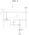
- FIG. 2 depicts an example of a conventional photodiode OLED coupled to a drive transistor M2.
- the drive transistor M2 is controlled by the voltage on its gate, which is stored on a capacitor C during an addressing phase.
- the addressing transistor M1 is turned on, allowing the desired voltage to transfer from the data line D to the capacitor C to reach the drive transistor M2.
- the photodiode OLED discharges the gate voltage stored on the capacitor C. This way, the photodiode OLED will no longer emit charge when the gate voltage on the drive transistor M2 reaches the threshold voltage, and the storage capacitor C will stop discharging.
- Transistor current that is output to the pixel has the following relationship to gate voltage V gs :
- I pixel ⁇ k V gs ⁇ V th ⁇
- k is a coefficient
- ⁇ is the mobility of the transistor
- V gs is the gate voltage
- V th is the threshold voltage.
- mobility ⁇ and threshold voltage V th are specific to each individual transistor in the display device.
- mobility ⁇ and threshold voltage V th of a single transistor also change with time and usage, for example due to temperature variation. Hence, over time and temperature changes, transistor characteristics between pixels can vary widely.
- Equation 2 takes into account difference in mobility ⁇ ⁇ and difference in threshold voltage ⁇ V th between pixels. Equation 2 also tracks the changes in mobility ⁇ and threshold voltage V th with time.
- I pixel ⁇ 0 + ⁇ ⁇ k V gs ⁇ V th 0 + ⁇ V th ⁇
- the model of Eq. 1 may not accurately predict the behavior of pixels as the size of the pixel transistor gets smaller and new material is introduced in transistor fabrication.
- LMS adaptation may work for finding parameters A and B.
- initial parameter values Ao and Bo may be set at 1 and 0, respectively.
- Parameters A and B are updated by testing a randomly chosen V gs0 in a set to see how the values of A, B, when used with the chosen V gs0 , affect I pixel.
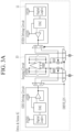
- FIG. 3A depicts one example of the sensing front end (SFE) circuitry that is incorporated into a display device, for example in column driver 9.
- the sensing front end circuitry includes a sensing circuit 10 and a driving circuit 11.
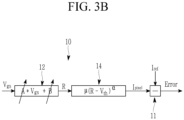
- FIG. 3B depicts an example of the sensing circuit 10 that is configured to compare a pixel current (I pixel ) output to a reference current (I ref ) to generate an error (Error).
- the reference current I ref is current of a predetermined value (e.g., 1 nA) that may be generated by a sensing front end (SFE) circuitry .
- the drive transistor M2 of a pixel receives an input voltage V gs to drive the pixel.
- a compensation unit 12 of the display device Based on the error (Error), a compensation unit 12 of the display device adjusts an input voltage V gs , which may correspond to a voltage applied to data line D, to generate a modified voltage (R).
- the compensation unit 12 of the front-end sensing circuit 10 outputs the modified voltage R to the gate of the drive transistor M2, to be used in place of V gs in the sensing circuit 10.
- a pixel current determination unit 14 uses the modified voltage R to determine the pixel current I pixel using mobility ( ⁇ ), threshold voltage (V th ), and exponent ( ⁇ ) according to a standard transistor model.
- a comparator unit 16 compares the pixel current I pixel with the reference current I ref to generate an error (Error), which gets fed back to the compensation unit 12.
- the compensation unit 12 may iteratively adjust the first parameter A and the second parameter B until the current output to the pixel (I pixel ) converges to the reference current (I ref ). Accordingly, color output by the pixel may converge to a desired level.
- the broken arrows over A and B in FIG. 1 indicate that the values of A and B are being updated by an adaptation circuit.
- compensation parameters A and B are optimized at values that compensate for the variation of ⁇ and V th such that I pixel stays the same across pixels for a given V gs0 . That is, A and B are tuned to fulfill the following ideal cases: B ⁇ V th 0 + ⁇ V th ⁇ ⁇ AV th 0 A ⁇ ⁇ 1 + ⁇ ⁇ 0
- At least four pairs of V gs0 and I pixel are used to tune A and B.
- LMS Least Mean Square
- a pentile 120Hz QHD display has 1560 x 1440 pixels. If each pixel had two sub-pixels, the number of sub-pixels would equal 4,492,800. Assuming a frame time of around 8.33 milliseconds, and assuming that each pixel requires 100 senses to converge, about 1% of the pixels may be sensed every frame.
- a method that reduces LMS adaptation or convergence time that is simple enough to be implemented without much extra hardware or cost is presented.
- the method entails using converged values of previous lines to set an initial value for a next line to shorten the convergence time.
- a smart gear-shifting technique is presented that allows gear shifting to happen at a desired time without waiting for a preset number of sensing operations.
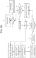
- FIG. 4A depicts a flowchart for a fast external pixel compensation process 50 in accordance with an embodiment of this disclosure.
- the process 50 starts by setting A 0 (L-1) and B 0 (L-1) for the first group/row (block 51), usually to a predetermined value such as 0 or 1. Then, LMS is performed to determine a first converged value A converged and a second converged value B converged for each pixel in a current group/row (block 52). If there is another group/row to process (block 53), the moving average of the first converged value A converged and the second converged value B converged are determined for each position/column in the group (block 54).
- the moving average of the first converged value A converged and the second converged value B converged are determined for each columnn in the row.
- the operation moves to the next group/row (the current group L in this example).
- the initial parameters Ao[L] and Bo[L] of each pixel in the group/row L is set to the moving average Amean of the first converged value A converged and the moving average Bmean of the second converged value B converged for the position/column of that pixel (block 56).
- Using a moving average of converged values from previous groups (e.g., L-1) as initial values for a current group (e.g., L) results in faster convergence for pixel compensation. Moving average is used primarily for initial, starting values of a new group, not used for subsequent iterations.
- the process 50 terminates (block 57).
- FIG. 4B depicts a modified LMS process 60, which includes an LMS process with modified gear shifting that is briefly shown in block 52 of FIG. 4A .
- FIG. 4B depicts the LMS process on the lefthand side and the modified gear shifting process on the righthand side.
- the modified code R n which is the parameter being converged, is determined based on input code G n (which may be V gs ) and compensation parameters A n and B n (block 61).
- the moving average R mean,n gets settled at the converging value of R n .
- the slope of R mean, n is related to the size of the gear, which affects speed of convergence. As used herein, the subscript "n" indicates one iteration for pixel, and the subscript "n+1" indicates a next iteration for the same pixel. If pixel parameters change faster than the time it takes for the parameters A and B to converge, the algorithm never converges. Hence, the speed at which convergence is reached affects how much benefit is derived from the voltage adjustments.
- the pixel output I pixel is calculated for each R n , for each cycle n.
- Eq. 6 above may be used with R n replacing V gs0 .
- the difference between pixel current I pixel and reference current I reference is determined (block 63).
- a n and B n are updated based on one or more step size and the difference (I pixel - I ref ) (block 64).
- the slope of R mean is checked for multiple pixels on a line.
- the iterative process continues until WIN number of iterations have been performed since the last R mean check.
- WIN is a time window index indicating the number of operations per pixel.
- R diff abs R mean , n ⁇ R mean , n ⁇ WIN + 1 .
- R diff ⁇ Limit n e.g. for each pixel in the group (block 69), and there is a next gear size (block 70)
- the gear size is changed (e.g., to a smaller gear) and the limit threshold, window size, and step sizes are adjusted according to the new step/gear settings (block 73).
- the process progresses to the next window (block 71).
- a gear is held for a fixed number of sensing operations before being switched to another gear.
- the conventional binary gear shift method does not allow the gear to be switched faster or slower, and have to go through the fixed number of sensing operations even if the number is clearly too high for some situations.
- the adaptive gear shift method of the present disclosure allows gear shift in a more optimized manner, based on R diff .
- the first converged value A converged and the second converged value B converged are determined for each pixel in the group/row based on the last parameter values A n and B n for the pixel.
- WIN sensing refers to the preselected number of sensing cycles that are required before a gear change is allowed.
- the first and second converged values A converged [L] and B converged [L] may be used to set a first initial value A 0 [L+1] and a second initial value B 0 [L+1] in block 56, for the next group L+1.
- Block 52, or the LMS process 60 depicted in FIG. 4B repeat for all the groups/rows in the display.
- modifying the values of the first parameter A n and the second parameter B n is done based on the step/gear size, which takes into account the difference between I pixel and I reference .
- the step/gear size is determined based on a moving average of modified volrages R mean, n for the pixel in group/row L.
- the step size may be adjusted in response to a change in the moving average of the modified input codes (e.g., voltages) relative to a predefind limit.
- the step size correlates with the predefined limit, as will be described in detail in reference to FIG. 11 below.
- a typical LMS adaptation process begins with preselected initial adaptation values Ao and Bo as the compensation parameters.
- initial adaptation parameter values Ao and Bo are used for every line.
- Ao and Bo as the starting point for every line
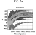
- a and B converge after about 25000 sense cycles.
- FIG. 5A and FIG. 5B show that, using the technique of starting with Ao and Bo for every line, each line takes about 25000 cycles to converge, even though the final values are different.
- the different plot lines represent different lines. There is not much difference in the number of cycles it takes to converge for each line, compared to for the preceding line. Every pixel compensation takes a long time to converge due to repeating of the same redundant steps as the previous line.
- the first and second compensation parameters A, B are set at initial values Ao and Bo, respectively, only for the first line/row of pixels.
- the initial compensation parameters A and B are not automatically set at Ao and Bo. Rather, initial compensation parameters A and B for line 2 are set at values that are based on the converged values of line 1, compensation parameters A and B for line 3 are set at values that are based on the converged values of line 2, etc. as described above in reference to FIG. 4A and FIG. 4B .
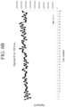
- FIG. 6A and FIG. 6B depict digitized values of compensation parameters A and B from line 1 to line 100 of the same column after convergence.
- initial values Ao and Bo are set to one. The plots confirm that starting a next line with the final value of the preceding line is likely to result in faster convergence.
- FIG. 7 depicts convergence for a compensation parameter A for 80 lines in the same column of a display where adaptation is done using the same Ao and Bo as initial values.
- the first plot line shows the converged values for each row.
- the second plot line which shows the moving average for each row, results in smoother convergence with smaller fluctuations than the converged values.
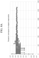
- FIG. 8A depicts a display where adaption is done using initial values Ao and Bo for every row
- FIG. 8B depicts the case where adaption for subsequent lines was done using the converged values of the former line(s).
- FIG. 8A it took about 750-1000 cycles to reach convergence.
- FIG. 8B it took about 100-120 cycles to reach convergence.
- a moving average of previously converged A and B values may be used as initial values. Using a moving average of converged parameters from previous lines as initial values for a subsequent line results in faster convergence for pixel compensation, as demonstrated by FIG. 8A and FIG. 8B .
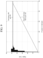
- FIG. 9 depicts plot A that shows convergence with a conventional gear shift, and plot B that shows convergence with no gear shift.
- the convergence with gear shift is achieved at about 80 cycles, whereas convergence without gear shift - but with previous-convergence-based initial parameter setting described above -- took about 475 cycles.
- the gear shift technique reached convergence about 6 times faster than LMS with no gear shift.
- FIG. 10(a) and FIG. 10(b) depict convergence of compensation parameters A and B, while FIG. 10(c) depicts R[n] of Equation 8, which in this case is V gs .
- FIG. 10(e) depicts the Gear Step Change.
- the five plots of FIG. 10(a), FIG. 10(b), FIG. 10(c), FIG. 10(d), and FIG. 10(e) are shown as separate plots for clarity, the y-axis values are taken along the same x-axis sense operations. While adaption of compensation parameters A and B is in progress, R n fluctuates heavily.
- FIG. 10(d) shows that in the x-axis range of ⁇ 1000 cycles, the absolute value quantity (R diff ) is large.
- the Limit[n] changes according to the fluctuations in R diff .
- the gear step changes dramatically when the R diff value in FIG. 10(d) is large.
- gear size goes down if R diff ⁇ Limit[n].
- R diff is consistently below Limit[n] as depicted in FIG. 10(d)
- the gear step size continually gets smaller throughout the plot.
- FIG. 11 depicts an example gear shift schedule table.
- the gear size starts off large (16X), and WIN cycle is set to 32 indicating that at least 32 cycles are run before the gear size is allowed to change, usually by one size down.
- Limit[n] indicates the maximum R diff value at which the gear size can go smaller. So, after 32 cycles (where 32 is the minimum # of cycles), if R diff is equal to or larger than Limit[n], another 32 cycles are run. If, on the other hand, R diff is smaller than Limit[n], the gear size goes down to the next size, which in this case is 8X. 32 cycles happen, then the R diff is compared to Limit[n]. If R diff ⁇ Limit[n], the gear size goes down to 4X.
- line L may start with the second largest gear size (8X in the table of FIG. 11 ).
- the finest gear or step size for line L may be 1 ⁇ 2X or 1 ⁇ 4X in the example of FIG. 11 .
- WIN cycles and Limit variables may be predetermined for each gear size, based on a heuristic process that takes into account environmental factors such as noise.
- the gear shift table may be different for the first line and the subsequent lines.
- FIG. 12A depicts a gear shift table for the first line
- FIG. 12B depicts a gear shift table for subsequent lines for the same display.
- the adaptation starts with a coarser or larger gear size for the first line than for the subsequent lines. More WIN cycles (32) are required for the first line than for a subsequent line (4). A wider range of gear sizes are available for the first line than for the other lines.
- FIG. 13 depicts the impact of the method of the disclosure on two example panels.
- use of the fast LMS method disclosed herein decreased the adaptation time for green pixels from 120.23 minutes to 8.63 minutes, and from 148.65 minutes to 8.93 minutes for red/blue pixels. This significant decrease in adaptation time is achieved without a significant effect on pixel uniformity (91.5% vs. 91.3%).
- use of the fast LMS method of the disclosure reduced the adaptation time from 117.55 minutes to 10.02 minutes for green pixels, and from 126.13 minutes to 10.80 minutes for red/blue pixels. As with Panel 1, this significant reduction in adaptation time is achieved without a noticeable degradation in pixel uniformity.
- the disclosed systems and methods may set parameters used for pixel compensation for a pixel in a group (e.g., a row).
- the disclosed systems and methods may converge more quickly as compared to systems and methods that update each pixel in a display device based on errors detected for that pixel.
- the concepts disclosed herein may be applied to various types of display devices, including but not limited to organic light emitting diode (OLED) display devices and liquid crystal display (LCD) devices.
- aspects of the systems and methods provided herein can be embodied in programming.
- Various aspects of the technology may be thought of as “products” or “articles of manufacture” typically in the form of machine (or processor) executable code and/or associated data that is carried on or embodied in a type of machine readable medium, such as a chip.
- Machine-executable code can be stored on an electronic storage unit, such as memory (e.g., read-only memory, random-access memory, flash memory) or a hard disk.
- “Storage” type media can include any or all of the tangible memory of the computers, processors or the like, or associated modules thereof, such as various semiconductor memories, tape drives, disk drives and the like, which may provide non-transitory storage at any time for the programming.
- terms such as computer or machine “readable medium” refer to any medium that participates in providing instructions to a processor for execution.
- the Least Mean Square calculation process may be implemented using a Field-Programmable Gate Array (FPGA) in the drive circuit (e.g., the sensing front end circuit) of a display device, or a computing device.
- FPGA Field-Programmable Gate Array
- a machine readable medium such as computer-executable code, may take many forms, including but not limited to, a tangible storage medium, a carrier wave medium or physical transmission medium.
- Non-volatile storage media include, for example, optical or magnetic disks, such as any of the storage devices in any computer(s) or the like, such as may be used to implement the databases, etc. shown in the drawings.
- Volatile storage media include dynamic memory, such as main memory of such a computer platform.
- Tangible transmission media include coaxial cables; copper wire and fiber optics, including the wires that comprise a bus within a computer system.
- Carrier-wave transmission media may take the form of electric or electromagnetic signals, or acoustic or light waves such as those generated during radio frequency (RF) and infrared (IR) data communications.
- RF radio frequency
- IR infrared
- Computer-readable media therefore include for example: a floppy disk, a flexible disk, hard disk, magnetic tape, any other magnetic medium, a CD-ROM, DVD or DVD-ROM, any other optical medium, punch cards paper tape, any other physical storage medium with patterns of holes, a RAM, a ROM, a PROM and EPROM, a FLASH-EPROM, any other memory chip or cartridge, a carrier wave transporting data or instructions, cables or links transporting such a carrier wave, or any other medium from which a computer may read programming code and/or data. Many of these forms of computer readable media may be involved in carrying one or more sequences of one or more instructions to a processor for execution.
Landscapes
- Engineering & Computer Science (AREA)
- Physics & Mathematics (AREA)
- Computer Hardware Design (AREA)
- General Physics & Mathematics (AREA)
- Theoretical Computer Science (AREA)
- Chemical & Material Sciences (AREA)
- Crystallography & Structural Chemistry (AREA)
- Control Of Indicators Other Than Cathode Ray Tubes (AREA)
Abstract
Description
- Different types of active matrix display devices are known today, including but not limited to organic light emitting diode (OLED) devices and liquid crystal display (LCD) devices.
FIG. 1 depicts an example of a conventional active matrix addressed display device that includes an array ofpixels 1, each of thepixels 1 having adisplay element 2. As shown, the display device comprises a panel having a plurality ofpixels 1 arranged in rows (L-1), L, (L+1), etc. and columns. Although a small number ofpixels 1 are shown inFIG. 1 for simplicity, a display panel comprises hundreds and thousands of pixels. Thepixels 1 are driven by arow driver 8 and acolumn driver 9, which receive and process data from asignal controller 7 and transmit signals on scan lines S and data lines D. - The display panel may have current-addressed
display elements 2. There are various ciruits for providing a controllable current through thedisplay element 2, and eachpixel 1 is configured to emit light based on a received current. The current that apixel 1 receives is controlled by a driving transistor. To cause the pixel to output a particular color, a display device may apply a voltage to the gate of the transistor based on the particular color. A storage capacitor may be included to hold the gate voltage after the addressing phase. - Often, during operation, characteristics (e.g., mobility and voltage threshold) of the transistor may change (e.g., due to heat). Application of high voltages above the threshold voltage causes large changes in threshold voltage over time. As not all the
pixels 1 are used the same way or stay on for the same amount of time, a large difference in the threshold voltages of transistors in different pixels may result. Accordingly, the transistor may output a first current value to the pixel responsive to a particular voltage value at a first time but output a second current value to the pixel responsive to the particular voltage value at a second time. The changes might not be consistent across the panel. Also, different drive transistors may have different characteristics due to manufacturing variation. These variations and differential aging may cause problems with the display device. - Given the large number of pixels in a display device, compensating for the transistor change for each pixel individually is a huge task. If temperature and ambient light change faster than the pixels can converge, there will be no convergence and no effective update. A fast and efficient method of dealing with the different changes of pixels in a display device is desired.
- A method of compensating for change in pixel performance is disclosed. The method entails dividing pixels into groups including a previous group L-1, a current group L and a next group L+1, determining a first converged value Aconverged[L] and a second converged value Bconverged[L] for each pixel in the current group L starting with a first initial value Ao[L] and a second initial value Bo[L], for each pixel in the current group L, determining a first moving average Amean[L] and a second moving average Bmean[L] as follows:


- In another aspect, the disclosure pertains to a display device that includes a plurality of pixels, each of the pixels including a light emitting element, wherein the light emitting element is coupled to a transistor that is controlled by a gate voltage Vgs; circuitry configured to adjust the gate voltage Vgs by dividing the pixels into groups including a previous group L-1, a current group L and a next group L+1, determining a first converged value Aconverged[L] and a second converged value Bconverged[L] for each pixel in the current group L starting with a first initial value Ao[L] and a second initial value Bo[L], for each pixel in the current group L, determining a first moving average Amean[L] and a second moving average Bmean[L] as follows:


- At least some of the above and other features of the invention are set out in the claims.
-
-
FIG. 1 depicts an example of a conventional active matrix addressed display device. -
FIG. 2 depicts an example of a conventional photodiode OLED coupled to a drive transistor. -
FIG. 3A depicts one example of the sensing front end (SFE) circuitry that is incorporated into a display device. -
FIG. 3B depicts a sensing circuit that may be incorporated into a display device. -
FIG. 4A depicts a flowchart for a fast external pixel compensation process in accordance with an embodiment of this disclosure. -
FIG. 4B depicts a flowchart for a Least Mean Square process with modified gear shift in accordance with an embodiment of this disclosure. -
FIG. 5A andFIG. 5B depict compensation parameter values as a function of iteration cycles wherein the same initial values are applied to every line. -
FIG. 6A andFIG. 6B depict digitized values of compensation parameters A and B fromline 1 toline 100 of the same column after convergence. -
FIG. 7 depicts convergence for a compensation parameter A for 80 lines in the same column of a display where adaptation is done using the same initial parameter values for every line. -
FIG. 8A depicts a display where adaption is done using initial values Ao and Bo for every row, andFIG. 8B depicts the case where adaption for non-first lines was done using the converged values of the former line(s) in accordance with an embodiment of the disclosure. -
FIG. 9 depicts plot A that shows convergence with a conventional gear shift, and plot B that shows convergence with no gear shift. -
FIG. 10(a), FIG. 10(b), FIG. 10(c), FIG. 10(d), and FIG. 10(e) depict compensation prameters, modified voltage, and gear size as they correlate with one another during adaptation, in accordance with an embodiment of the disclosure. -
FIG. 11 depicts an example gear shift schedule table. -
FIG. 12A depicts a gear shift table for the first line, andFIG. 12B depicts a gear shift table for subsequent lines for the same display. -
FIG. 13 depicts the impact of the method of the disclosure on two example panels. - An adaptation method for faster pixel convergence is disclosed. The method according to the disclosure entails starting the adaptation process for a line or row of pixels using a converged value from the previous line or row. The method according to the disclosure further entails a dynamic gear shifting method that allows gear size to be changed after different numbers of sensing cycles depending on the rate of convergence of parameter values. For simplicity, a line/row of pixels are used as an example group of spatially correlated pixels in this description. However, it should be understood that a "group" of pixels is not restricted to being a single line of pixels, and may represent any number of pixels in different arrangements, according to spatial correlation in the display device.
-
FIG. 2 depicts an example of a conventional photodiode OLED coupled to a drive transistor M2. The drive transistor M2 is controlled by the voltage on its gate, which is stored on a capacitor C during an addressing phase. During the addressing phase, the addressing transistor M1 is turned on, allowing the desired voltage to transfer from the data line D to the capacitor C to reach the drive transistor M2. The photodiode OLED discharges the gate voltage stored on the capacitor C. This way, the photodiode OLED will no longer emit charge when the gate voltage on the drive transistor M2 reaches the threshold voltage, and the storage capacitor C will stop discharging. - Transistor current that is output to the pixel (Ipixel) has the following relationship to gate voltage Vgs:

Equation 2 takes into account difference in mobility Δµ and difference in threshold voltage ΔVth between pixels.Equation 2 also tracks the changes in mobility µ and threshold voltage Vth with time.
- The model of Eq. 1 may not accurately predict the behavior of pixels as the size of the pixel transistor gets smaller and new material is introduced in transistor fabrication. To compensate for mismatches in mobility µ and threshold voltage Vth among different pixels on a same panel, the following model may be used:


- Combining Eq. 2 with Eq. 3 yields the following:

- Although [Eq. 4] shows Ipixel as a non-linear function of Vgs0, LMS adaptation may work for finding parameters A and B. In one embodiment, initial parameter values Ao and Bo may be set at 1 and 0, respectively. Parameters A and B are updated by testing a randomly chosen Vgs0 in a set to see how the values of A, B, when used with the chosen Vgs0, affect Ipixel.
-
FIG. 3A depicts one example of the sensing front end (SFE) circuitry that is incorporated into a display device, for example incolumn driver 9. As shown, the sensing front end circuitry includes asensing circuit 10 and a drivingcircuit 11.FIG. 3B depicts an example of thesensing circuit 10 that is configured to compare a pixel current (Ipixel) output to a reference current (Iref) to generate an error (Error). The reference current Iref is current of a predetermined value (e.g., 1 nA) that may be generated by a sensing front end (SFE) circuitry . As shown inFIG. 3B , the drive transistor M2 of a pixel receives an input voltage Vgs to drive the pixel. Based on the error (Error), acompensation unit 12 of the display device adjusts an input voltage Vgs, which may correspond to a voltage applied to data line D, to generate a modified voltage (R). Thecompensation unit 12 of the front-end sensing circuit 10 outputs the modified voltage R to the gate of the drive transistor M2, to be used in place of Vgs in thesensing circuit 10. A pixelcurrent determination unit 14 uses the modified voltage R to determine the pixel current Ipixel using mobility (µ), threshold voltage (Vth), and exponent (α) according to a standard transistor model. Acomparator unit 16 compares the pixel current Ipixel with the reference current Iref to generate an error (Error), which gets fed back to thecompensation unit 12. Some components depicted inFIG. 3B may be outside thesensing circuit 10 in other embodiments. - In the example of
FIG. 3B , the modified input voltage R into the drive transistor M2 is determined as follows:
compensation unit 12 may iteratively adjust the first parameter A and the second parameter B until the current output to the pixel (Ipixel) converges to the reference current (Iref). Accordingly, color output by the pixel may converge to a desired level. InFIG. 3B , the broken arrows over A and B inFIG. 1 indicate that the values of A and B are being updated by an adaptation circuit. - Eventually, compensation parameters A and B are optimized at values that compensate for the variation of µ and Vth such that Ipixel stays the same across pixels for a given Vgs0. That is, A and B are tuned to fulfill the following ideal cases:

- A and B fulfilling the ideal case conditions results in Ipixel becoming independent of Δµ and ΔVth, as follows:

- In some cases, at least four pairs of Vgs0 and Ipixel are used to tune A and B.
- Actual LMS adaptation may be simplified for easy implementation with digital logic, as follows:


- A[n-1] and B[n-1] are parameters A and B at sense measurement cycle (n-1);
- A[n] and B[n] are parameters A and B at sense measurement cycle n;
- Din[n-1] is 1 when Ipixel at cycle (n-1) is less than the desired value, 0 otherwise (D being the difference);
- sign (X) is +1 when X > 0, -1 otherwise; and
- ΔA and ΔB are step size of A and B, respectively, for each change per cycle.
- Often, calibration is done to make sure the outcome is accurate. Least Mean Square (LMS) adaptive process, among other methods, may be used to calibrate the pixels so that Ipixel is substantially constant. However, running the LMS process on each individual pixel of a display device and converging each pixel to a compensation factor may take too much time. For example, a pentile 120Hz QHD display has 1560 x 1440 pixels. If each pixel had two sub-pixels, the number of sub-pixels would equal 4,492,800. Assuming a frame time of around 8.33 milliseconds, and assuming that each pixel requires 100 senses to converge, about 1% of the pixels may be sensed every frame. It would take 100 x 100 frames for all the pixels to converge, which would take 83 seconds at 120 Hz. Eighty-three seconds is a long time for temperature and ambient light to remain constant on a display device. Conditions within the display device (e.g., temperature) may change before pixels converge, resulting in inaccurate pixel outputs. In mass production, calibration time of less than 10 seconds is desired. The system and method disclosed herein overcome this issue by achieving a faster convergence.
- In this disclosure, a method that reduces LMS adaptation or convergence time that is simple enough to be implemented without much extra hardware or cost is presented. In one aspect, the method entails using converged values of previous lines to set an initial value for a next line to shorten the convergence time. In another aspect, a smart gear-shifting technique is presented that allows gear shifting to happen at a desired time without waiting for a preset number of sensing operations.
-
FIG. 4A depicts a flowchart for a fast externalpixel compensation process 50 in accordance with an embodiment of this disclosure. As shown, theprocess 50 starts by setting A0(L-1) and B0(L-1) for the first group/row (block 51), usually to a predetermined value such as 0 or 1. Then, LMS is performed to determine a first converged value Aconverged and a second converged value Bconverged for each pixel in a current group/row (block 52). If there is another group/row to process (block 53), the moving average of the first converged value Aconverged and the second converged value Bconverged are determined for each position/column in the group (block 54). Where a group is a row, the moving average of the first converged value Aconverged and the second converged value Bconverged are determined for each columnn in the row. Where the previous group/row (L-1) is the very first group/row, a first moving average Amean[L-1] is determined to be the same as the first converged value Aconverged (i.e., Amean[L-1] = A[L-1]). Similarly, where the previous group/row is the very first group/row, a second moving average Bmean[L-1] is determined to be the same as the second converged value Bconverged (i.e., Bmean [L-1] = B[L-1]). For all other groups/rows, a moving average (herein used interchangeably with "mean") may be determined as follows:

- In
block 55, the operation moves to the next group/row (the current group L in this example). The initial parameters Ao[L] and Bo[L] of each pixel in the group/row L is set to the moving average Amean of the first converged value Aconverged and the moving average Bmean of the second converged value Bconverged for the position/column of that pixel (block 56). Using a moving average of converged values from previous groups (e.g., L-1) as initial values for a current group (e.g., L) results in faster convergence for pixel compensation. Moving average is used primarily for initial, starting values of a new group, not used for subsequent iterations. When the LMS process is performed for all the groups/rows, theprocess 50 terminates (block 57). -
FIG. 4B depicts a modifiedLMS process 60, which includes an LMS process with modified gear shifting that is briefly shown inblock 52 ofFIG. 4A .FIG. 4B depicts the LMS process on the lefthand side and the modified gear shifting process on the righthand side. For each pixel in a group/row L, the modified code Rn, which is the parameter being converged, is determined based on input code Gn (which may be Vgs) and compensation parameters An and Bn (block 61). A generic equation for LMS compensation may be as shown below:
- In
block 62, the pixel output Ipixel is calculated for each Rn, for each cycle n. For example, Eq. 6 above may be used with Rn replacing Vgs0. For each pixel in the group, the difference between pixel current Ipixel and reference current Ireference is determined (block 63). For each pixel in the group/row, An and Bn are updated based on one or more step size and the difference (Ipixel - Iref) (block 64). Inblock 65, the moving average of Rmean, n may be determined as follows:
block 66, the iterative process continues until WIN number of iterations have been performed since the last Rmean check. More specifically, inblock 66, if it is determined that the WIN number of iterations has not been performed, then another iteration is done (block 67) and blocks 61 through 66 are repeated untilblock 66 determines that the WIN number of iterations has been performed. WIN is a time window index indicating the number of operations per pixel. - If a predetermined WIN number of iterations has been performed since last Rmean check (block 66), then for each pixel in the group/row, Rdiff is determined as follows (block 68):

- If Rdiff < Limitn, e.g. for each pixel in the group (block 69), and there is a next gear size (block 70), then the gear size is changed (e.g., to a smaller gear) and the limit threshold, window size, and step sizes are adjusted according to the new step/gear settings (block 73). The process progresses to the next window (block 71). In a conventional binary gear shift method, a gear is held for a fixed number of sensing operations before being switched to another gear. The conventional binary gear shift method does not allow the gear to be switched faster or slower, and have to go through the fixed number of sensing operations even if the number is clearly too high for some situations. The adaptive gear shift method of the present disclosure allows gear shift in a more optimized manner, based on Rdiff.
- If, in
block 70, it is determined that there is no "next size gear," (i.e. no next setting of step size, limit threshold and window size) then the first converged value Aconverged and the second converged value Bconverged are determined for each pixel in the group/row based on the last parameter values An and Bn for the pixel. - As used herein, "WIN sensing" refers to the preselected number of sensing cycles that are required before a gear change is allowed. The first and second converged values Aconverged[L] and Bconverged[L] may be used to set a first initial value A0[L+1] and a second initial value B0[L+1] in
block 56, for the next group L+1.Block 52, or theLMS process 60 depicted inFIG. 4B , repeat for all the groups/rows in the display. In theLMS process 60, modifying the values of the first parameter An and the second parameter Bn is done based on the step/gear size, which takes into account the difference between Ipixel and Ireference. More specifically, the step/gear size is determined based on a moving average of modified volrages Rmean, n for the pixel in group/row L. In one example, the step size may be adjusted in response to a change in the moving average of the modified input codes (e.g., voltages) relative to a predefind limit. The step size correlates with the predefined limit, as will be described in detail in reference toFIG. 11 below. - A typical LMS adaptation process begins with preselected initial adaptation values Ao and Bo as the compensation parameters. In an embodiment where the pixels are grouped according to lines/rows, initial adaptation parameter values Ao and Bo are used for every line. With Ao and Bo as the starting point for every line, A and B converge after about 25000 sense cycles.
FIG. 5A andFIG. 5B show that, using the technique of starting with Ao and Bo for every line, each line takes about 25000 cycles to converge, even though the final values are different. The different plot lines represent different lines. There is not much difference in the number of cycles it takes to converge for each line, compared to for the preceding line. Every pixel compensation takes a long time to converge due to repeating of the same redundant steps as the previous line. However, the converged A and B values of adjacent lines on the same column are often close to each other. This data suggests that instead of starting the next line with the same initial parameter values Ao, Bo as the previous line, convergence could be reached faster by starting with an initial value that is based on the converged value of the previous group. - In accordance with an embodiment of the present disclosure, the first and second compensation parameters A, B are set at initial values Ao and Bo, respectively, only for the first line/row of pixels. For lines following the first line, the initial compensation parameters A and B are not automatically set at Ao and Bo. Rather, initial compensation parameters A and B for
line 2 are set at values that are based on the converged values ofline 1, compensation parameters A and B forline 3 are set at values that are based on the converged values ofline 2, etc. as described above in reference toFIG. 4A andFIG. 4B . -
FIG. 6A andFIG. 6B depict digitized values of compensation parameters A and B fromline 1 to line 100 of the same column after convergence. In this particular example, initial values Ao and Bo are set to one. The plots confirm that starting a next line with the final value of the preceding line is likely to result in faster convergence. -
FIG. 7 depicts convergence for a compensation parameter A for 80 lines in the same column of a display where adaptation is done using the same Ao and Bo as initial values. The first plot line shows the converged values for each row. The second plot line, which shows the moving average for each row, results in smoother convergence with smaller fluctuations than the converged values. -
FIG. 8A depicts a display where adaption is done using initial values Ao and Bo for every row, andFIG. 8B depicts the case where adaption for subsequent lines was done using the converged values of the former line(s). InFIG. 8A , it took about 750-1000 cycles to reach convergence. In contrast, when using the converged values of preceding lines as the starting point of convergence for the next line as shown inFIG. 8B , it took about 100-120 cycles to reach convergence. In one embodiment, a moving average of previously converged A and B values may be used as initial values. Using a moving average of converged parameters from previous lines as initial values for a subsequent line results in faster convergence for pixel compensation, as demonstrated byFIG. 8A andFIG. 8B . - To achieve an even faster LMS adaptation, a binary gear shift method may be utilized.
FIG. 9 depicts plot A that shows convergence with a conventional gear shift, and plot B that shows convergence with no gear shift. As can be seen, the convergence with gear shift is achieved at about 80 cycles, whereas convergence without gear shift - but with previous-convergence-based initial parameter setting described above -- took about 475 cycles. The gear shift technique reached convergence about 6 times faster than LMS with no gear shift. -
FIG. 10(a) and FIG. 10(b) depict convergence of compensation parameters A and B, whileFIG. 10(c) depicts R[n] ofEquation 8, which in this case is Vgs.FIG. 10(d) and depicts the value abs(Rmean, n - Rmean, [n-WIN+1]), andFIG. 10(e) depicts the Gear Step Change. Although the five plots ofFIG. 10(a), FIG. 10(b), FIG. 10(c), FIG. 10(d), and FIG. 10(e) are shown as separate plots for clarity, the y-axis values are taken along the same x-axis sense operations. While adaption of compensation parameters A and B is in progress, Rn fluctuates heavily. However, as the compensation parameters A and B converge around 2500 sense operations, Vgs converges around 3000 sense operations. In the early part of the sense operations (<1000 cycles), the fluctuations of compensation parameters A and B are large.FIG. 10(d) shows that in the x-axis range of < 1000 cycles, the absolute value quantity (Rdiff) is large. The Limit[n] changes according to the fluctuations in Rdiff. As shown inFIG. 10(e) , the gear step changes dramatically when the Rdiff value inFIG. 10(d) is large. However, as Rdiff decreases, so does the gear size. According to the rule inblock 60 ofFIG. 5 , gear size goes down if Rdiff < Limit[n]. As Rdiff is consistently below Limit[n] as depicted inFIG. 10(d) , the gear step size continually gets smaller throughout the plot. -
FIG. 11 depicts an example gear shift schedule table. As shown, the gear size starts off large (16X), and WIN cycle is set to 32 indicating that at least 32 cycles are run before the gear size is allowed to change, usually by one size down. Limit[n] indicates the maximum Rdiff value at which the gear size can go smaller. So, after 32 cycles (where 32 is the minimum # of cycles), if Rdiff is equal to or larger than Limit[n], another 32 cycles are run. If, on the other hand, Rdiff is smaller than Limit[n], the gear size goes down to the next size, which in this case is 8X. 32 cycles happen, then the Rdiff is compared to Limit[n]. If Rdiff < Limit[n], the gear size goes down to 4X. If, on the other hand, Rdiff ≥ Limit[n], 32 cycles are run again before the comparison to Limit[n] is made again, for the first line (only 4 cycles are needed for a second and subsequent line). With the method of the disclosure where the initial compensation values of second line L is set based on the converged value of the first line (L-1), line L may start with the second largest gear size (8X in the table ofFIG. 11 ). The finest gear or step size for line L may be ½X or ¼X in the example ofFIG. 11 . WIN cycles and Limit variables may be predetermined for each gear size, based on a heuristic process that takes into account environmental factors such as noise. - When the initial parameters of non-first lines are set using the converged parameters of the preceding line(s), the gear shift table may be different for the first line and the subsequent lines.
FIG. 12A depicts a gear shift table for the first line, andFIG. 12B depicts a gear shift table for subsequent lines for the same display. As shown, the adaptation starts with a coarser or larger gear size for the first line than for the subsequent lines. More WIN cycles (32) are required for the first line than for a subsequent line (4). A wider range of gear sizes are available for the first line than for the other lines. -
FIG. 13 depicts the impact of the method of the disclosure on two example panels. ForPanel 1, use of the fast LMS method disclosed herein decreased the adaptation time for green pixels from 120.23 minutes to 8.63 minutes, and from 148.65 minutes to 8.93 minutes for red/blue pixels. This significant decrease in adaptation time is achieved without a significant effect on pixel uniformity (91.5% vs. 91.3%). Similarly, forPanel 2, use of the fast LMS method of the disclosure reduced the adaptation time from 117.55 minutes to 10.02 minutes for green pixels, and from 126.13 minutes to 10.80 minutes for red/blue pixels. As withPanel 1, this significant reduction in adaptation time is achieved without a noticeable degradation in pixel uniformity. - Accordingly, the disclosed systems and methods may set parameters used for pixel compensation for a pixel in a group (e.g., a row). Thus, the disclosed systems and methods may converge more quickly as compared to systems and methods that update each pixel in a display device based on errors detected for that pixel. The concepts disclosed herein may be applied to various types of display devices, including but not limited to organic light emitting diode (OLED) display devices and liquid crystal display (LCD) devices.
- Aspects of the systems and methods provided herein can be embodied in programming. Various aspects of the technology may be thought of as "products" or "articles of manufacture" typically in the form of machine (or processor) executable code and/or associated data that is carried on or embodied in a type of machine readable medium, such as a chip. Machine-executable code can be stored on an electronic storage unit, such as memory (e.g., read-only memory, random-access memory, flash memory) or a hard disk. "Storage" type media can include any or all of the tangible memory of the computers, processors or the like, or associated modules thereof, such as various semiconductor memories, tape drives, disk drives and the like, which may provide non-transitory storage at any time for the programming. As used herein, unless restricted to non-transitory, tangible "storage" media, terms such as computer or machine "readable medium" refer to any medium that participates in providing instructions to a processor for execution.
- The Least Mean Square calculation process may be implemented using a Field-Programmable Gate Array (FPGA) in the drive circuit (e.g., the sensing front end circuit) of a display device, or a computing device. A machine readable medium, such as computer-executable code, may take many forms, including but not limited to, a tangible storage medium, a carrier wave medium or physical transmission medium. Non-volatile storage media include, for example, optical or magnetic disks, such as any of the storage devices in any computer(s) or the like, such as may be used to implement the databases, etc. shown in the drawings. Volatile storage media include dynamic memory, such as main memory of such a computer platform. Tangible transmission media include coaxial cables; copper wire and fiber optics, including the wires that comprise a bus within a computer system. Carrier-wave transmission media may take the form of electric or electromagnetic signals, or acoustic or light waves such as those generated during radio frequency (RF) and infrared (IR) data
communications. Common forms of computer-readable media therefore include for example: a floppy disk, a flexible disk, hard disk, magnetic tape, any other magnetic medium, a CD-ROM, DVD or DVD-ROM, any other optical medium, punch cards paper tape, any other physical storage medium with patterns of holes, a RAM, a ROM, a PROM and EPROM, a FLASH-EPROM, any other memory chip or cartridge, a carrier wave transporting data or instructions, cables or links transporting such a carrier wave, or any other medium from which a computer may read programming code and/or data. Many of these forms of computer readable media may be involved in carrying one or more sequences of one or more instructions to a processor for execution. - While preferred embodiments of the present disclosure have been shown and described herein, it will be obvious to those skilled in the art that such embodiments are provided by way of example only and are not meant to be construed in a limiting sense. It is not intended that the invention be limited by the specific examples provided within the specification. Numerous variations, changes, and substitutions will now occur to those skilled in the art without departing from the invention. Furthermore, it shall be understood that all aspects of the invention are not limited to the specific depictions, configurations or relative proportions set forth herein which depend upon a variety of conditions and variables. It should be understood that various alternatives to the embodiments of the invention described herein may be employed in practicing the invention. It is therefore contemplated that the invention shall also cover any such alternatives, modifications, variations or equivalents. It is intended that the following claims define the scope of the invention and that methods and structures within the scope of these claims and their equivalents be covered thereby.
Claims (17)
- A method of compensating for change in pixel performance, comprising:dividing pixels into groups including a previous group L-1, a current group L and a next group L+1;determining a first converged value Aconverged[L] and a second converged value Bconverged[L] for each pixel in the current group L starting with a first initial value Ao[L] and a second initial value Bo[L];for each pixel in the current group L, determining a first moving average Amean[L] and a second moving average Bmean[L] as follows:

 wherein Amean[L-1] is a first moving average of a pixel in the corresponding column in the previous group L-1,Bmean[L-1] is a second moving average of a pixel in the corresponding column in the previous group L-1, andK is a moving average window;for the next group L+1, setting a first initial value A0[L+1] and a second initial value B0[L+1] of each pixel to Amean[L] and Bmean[L].
 - The method of claim 1, wherein the pixels are arranged in rows and each of the previous group L-1, the current group L and the next group L+1 is one of the rows.
- The method of claim 1 or claim 2, further comprising determining the first initial value Ao[L] and the second initial value Bo[L] for each pixel based on Amean[L-1] and Bmean[L-1], wherein, optionally, the method further comprises setting the moving averages Amean[L] and Bmean[L] to Aconverged[L] and Bconverged[L] for the current group L upon determining that there is no previous group L-1.
- The method of any preceding claim further comprising changing a gear setting for convergence to Aconverged[L] and Bconverged[L] according to speed of convergence.
- The method of any preceding claim, wherein the determining of a first converged value Aconverged[L] and a second converged value Bconverged[L] for each pixel comprises:
for each pixel in the current group L, iteratively determining a modified code Rn = AnGn + Bn wherein Gn is an input code and n indicates an number of iteration, and first iteration is done using the first initial value Ao[L] and the second initial value Bo[L] as An and Bn. - The method of claim 5, wherein the determining of the first converged value Aconverged[L] and the second converged value Bconverged[L] for each pixel comprises:for each pixel in the current group L, applying the modified code Rn to generate pixel current Ipixel, by substituting Rn into Vgs0 wherein Ipixel = µ 0 k(V gs0 - V th
0 ) α ;comparing Ipixel with a predefined reference current value Ireference to generate ΔI;adjusting An and Bn for each pixel in the group L, based on ΔI and step size;determining Rmean,n for pixels in the current group L;determining a difference Rdiff for each pixel in the current group L, wherein Rdiff is a difference between Rmean for current window of WIN iterations and Rmean for previous window; andchanging step size if Rdiff satisfies a limit threshold. - The method of claim 6 further comprising adjusting at least one of the limit threshold and the window size.
- The method of claim 6 or claim 7, wherein changing the step size comprises adjusting to a smaller step size if Rdiff < Limitn, and wherein, optionally, the method further comprises determining the first converged value Aconverged and the second converged value Bconverged for each pixel in the current group L based on the latest first value An and the second value Bn if there is no next gear size.
- The method of any one of claims 6 - 8, further comprising performing a WIN number of iterations before determining the difference Rdiff.
- A display device comprising:a plurality of pixels, each of the pixels including a light emitting element, wherein the light emitting element is coupled to a transistor that is controlled by a gate voltage Vgs;circuitry configured to adjust the gate voltage Vgs by:dividing the pixels into groups including a previous group L-1, a current group L and a next group L+1;determining a first converged value Aconverged[L] and a second converged value Bconverged[L] for each pixel in the current group L starting with a first initial value Ao[L] and a second initial value Bo[L];for each pixel in the current group L, determining a first moving average Amean[L] and a second moving average Bmean[L] as follows:

 wherein Amean[L-1] is a first moving average of a pixel in the corresponding column in the previous group L-1,Bmean[L-1] is a second moving average of a pixel in the corresponding column in the previous group L-1, andK is a moving average window;for the next group L+1, setting a first initial value A0[L+1] and a second initial value B0[L+1] of each pixel to Amean[L] and Bmean[L].
 - The display device of claim 10, wherein the pixels are arranged in rows and each of the previous group L-1, the current group L and the next group L+1 is one of the rows.
- The display device of claim 10 or claim 11, wherein the circuitry is configured to adjust the gate voltage Vgs by setting the moving averages Amean[L] and Bmean[L] to Aconverged[L] and Bconverged[L] for the current group L upon determining that there is no previous group L-1.
- The display device of any one of claims 10 - 12, wherein the circuitry is configured to change a gear setting for convergence to Aconverged[L] and Bconverged[L] according to speed of convergence.
- The display device of any one of claims 10 - 13, wherein the circuitry is configured to determine the first converged value Aconverged[L] and the second converged value Bconverged[L] for each pixel by:for each pixel in the current group L, applying a modified code Rn to generate pixel current Ipixel, by substituting Rn into Vgs0 wherein Ipixel = µ 0 k(V gs0 - V th
0 ) α , wherein the modified code Rn = AnGn + Bn wherein Gn is an input code and n indicates an number of iteration, and first iteration is done using the first initial value Ao[L] and the second initial value Bo[L] as An and Bn;comparing Ipixel with a predefined reference current value Ireference to generate ΔI;adjusting An and Bn for each pixel in the group L, based on ΔI and step size;determining Rmean,n for pixels in the current group L;determining a difference Rdiff for each pixel in the current group L, wherein Rdiff is a difference between Rmean for current window of WIN iterations and Rmean for previous window; andchanging step size if Rdiff satisfies a limit threshold. - The display device of claim 14, wherein the circuitry is configured to adjust at least one of the limit threshold and the window size.
- The display device of claim 14 or claim 15, wherein the circuitry is configured to change the step size by adjusting to a smaller step size if Rdiff < Limitn, wherein, optionally, the circuitry is configured to determine the first converged value Aconverged and the second converged value Bconverged for each pixel in the current group L based on the latest first parameter value An and the second parameter value Bn if there is no next gear size.
- The display device of any one of claims 10 - 16, wherein the circuitry is configured to perform a WIN number of iterations before determining the difference Rdiff.
Applications Claiming Priority (2)
| Application Number | Priority Date | Filing Date | Title |
|---|---|---|---|
| US202163284811P | 2021-12-01 | 2021-12-01 | |
| US17/678,366 US11615739B1 (en) | 2021-12-01 | 2022-02-23 | Fast external pixel compensation in a display panel |
Publications (1)
| Publication Number | Publication Date |
|---|---|
| EP4191572A1 true EP4191572A1 (en) | 2023-06-07 |
Family
ID=84367653
Family Applications (1)
| Application Number | Title | Priority Date | Filing Date |
|---|---|---|---|
| EP22210360.8A Withdrawn EP4191572A1 (en) | 2021-12-01 | 2022-11-29 | Display apparatus and driving method thereof |
Country Status (3)
| Country | Link |
|---|---|
| EP (1) | EP4191572A1 (en) |
| KR (1) | KR20230083207A (en) |
| CN (1) | CN116206563A (en) |
Citations (3)
| Publication number | Priority date | Publication date | Assignee | Title |
|---|---|---|---|---|
| EP3038091A2 (en) * | 2014-12-24 | 2016-06-29 | LG Display Co., Ltd. | Organic light emitting diode display and method for sensing characteristic thereof |
| EP3822960A1 (en) * | 2019-11-14 | 2021-05-19 | Samsung Display Co., Ltd. | Display device and method of driving the same |
| EP3971879A1 (en) * | 2020-09-22 | 2022-03-23 | Samsung Display Co., Ltd. | Multi-pixel collective adjustment for steady state tracking of parameters |
-
2022
- 2022-07-13 KR KR1020220086437A patent/KR20230083207A/en active Pending
- 2022-11-29 EP EP22210360.8A patent/EP4191572A1/en not_active Withdrawn
- 2022-11-29 CN CN202211513434.2A patent/CN116206563A/en active Pending
Patent Citations (3)
| Publication number | Priority date | Publication date | Assignee | Title |
|---|---|---|---|---|
| EP3038091A2 (en) * | 2014-12-24 | 2016-06-29 | LG Display Co., Ltd. | Organic light emitting diode display and method for sensing characteristic thereof |
| EP3822960A1 (en) * | 2019-11-14 | 2021-05-19 | Samsung Display Co., Ltd. | Display device and method of driving the same |
| EP3971879A1 (en) * | 2020-09-22 | 2022-03-23 | Samsung Display Co., Ltd. | Multi-pixel collective adjustment for steady state tracking of parameters |
Also Published As
| Publication number | Publication date |
|---|---|
| CN116206563A (en) | 2023-06-02 |
| KR20230083207A (en) | 2023-06-09 |
Similar Documents
| Publication | Publication Date | Title |
|---|---|---|
| US9607544B2 (en) | Brightness compensating method and self-illuminating display device | |
| US8456414B2 (en) | Gamma adjustment with error diffusion for electrophoretic displays | |
| JP6657164B2 (en) | Organic light emitting display and driving method thereof | |
| KR100515622B1 (en) | Method of manufacturing image forming apparatus | |
| EP3016095B1 (en) | Organic light emitting diode display device and method of driving the same | |
| KR102449369B1 (en) | Display device and method of testing a display device | |
| US7973745B2 (en) | Organic EL display module and manufacturing method of the same | |
| CN115985269B (en) | Brightness compensation method and device, and computer readable storage medium | |
| US10580371B2 (en) | Data driving module for driving display panel, data driving method and display device | |
| EP3971879B1 (en) | Multi-pixel collective adjustment for steady state tracking of parameters | |
| US11615739B1 (en) | Fast external pixel compensation in a display panel | |
| CN115775533B (en) | Display panel brightness correction method, device, equipment and storage medium | |
| US12586505B2 (en) | Grayscale compensation method, apparatus and system, display driving method, apparatus and system, and chip and medium | |
| EP4191572A1 (en) | Display apparatus and driving method thereof | |
| CN114341969A (en) | Display aging compensation | |
| EP2065879A1 (en) | Liquid crystal panel drive device, liquid crystal panel drive method, liquid crystal display, and on-vehicle display | |
| CN106856083B (en) | Apparatus and method for correcting gamma set data | |
| CN115938321A (en) | Gamma Amplifier and Gamma Voltage Generator | |
| KR20200042349A (en) | De Mura Method of Display Panel and De-Mura Module | |
| CN105761671A (en) | System and method for extracting correlation curves of organic light emitting devices | |
| KR102492805B1 (en) | Display panel and method of testing the same | |
| JP2020144343A (en) | Display devices, control devices, and control methods for display devices | |
| KR102284755B1 (en) | Display Apparatus and Display Control Apparatus | |
| CN114446247A (en) | Display device and method of driving the same | |
| JP5592592B2 (en) | Automatic adjustment method |
Legal Events
| Date | Code | Title | Description |
|---|---|---|---|
| PUAI | Public reference made under article 153(3) epc to a published international application that has entered the european phase |
Free format text: ORIGINAL CODE: 0009012 |
|
| STAA | Information on the status of an ep patent application or granted ep patent |
Free format text: STATUS: THE APPLICATION HAS BEEN PUBLISHED |
|
| AK | Designated contracting states |
Kind code of ref document: A1 Designated state(s): AL AT BE BG CH CY CZ DE DK EE ES FI FR GB GR HR HU IE IS IT LI LT LU LV MC ME MK MT NL NO PL PT RO RS SE SI SK SM TR |
|
| STAA | Information on the status of an ep patent application or granted ep patent |
Free format text: STATUS: REQUEST FOR EXAMINATION WAS MADE |
|
| 17P | Request for examination filed |
Effective date: 20231129 |
|
| RBV | Designated contracting states (corrected) |
Designated state(s): AL AT BE BG CH CY CZ DE DK EE ES FI FR GB GR HR HU IE IS IT LI LT LU LV MC ME MK MT NL NO PL PT RO RS SE SI SK SM TR |
|
| GRAP | Despatch of communication of intention to grant a patent |
Free format text: ORIGINAL CODE: EPIDOSNIGR1 |
|
| STAA | Information on the status of an ep patent application or granted ep patent |
Free format text: STATUS: GRANT OF PATENT IS INTENDED |
|
| GRAJ | Information related to disapproval of communication of intention to grant by the applicant or resumption of examination proceedings by the epo deleted |
Free format text: ORIGINAL CODE: EPIDOSDIGR1 |
|
| STAA | Information on the status of an ep patent application or granted ep patent |
Free format text: STATUS: REQUEST FOR EXAMINATION WAS MADE |
|
| GRAP | Despatch of communication of intention to grant a patent |
Free format text: ORIGINAL CODE: EPIDOSNIGR1 |
|
| STAA | Information on the status of an ep patent application or granted ep patent |
Free format text: STATUS: GRANT OF PATENT IS INTENDED |
|
| INTG | Intention to grant announced |
Effective date: 20250715 |
|
| INTC | Intention to grant announced (deleted) | ||
| INTG | Intention to grant announced |
Effective date: 20250801 |
|
| STAA | Information on the status of an ep patent application or granted ep patent |
Free format text: STATUS: THE APPLICATION IS DEEMED TO BE WITHDRAWN |
|
| 18D | Application deemed to be withdrawn |
Effective date: 20251202 |