EP4191381A1 - Maximum current suppression for power management in a multi-core system - Google Patents
Maximum current suppression for power management in a multi-core system Download PDFInfo
- Publication number
- EP4191381A1 EP4191381A1 EP22211364.9A EP22211364A EP4191381A1 EP 4191381 A1 EP4191381 A1 EP 4191381A1 EP 22211364 A EP22211364 A EP 22211364A EP 4191381 A1 EP4191381 A1 EP 4191381A1
- Authority
- EP
- European Patent Office
- Prior art keywords
- current
- processor cores
- management circuit
- throttle
- processor
- Prior art date
- Legal status (The legal status is an assumption and is not a legal conclusion. Google has not performed a legal analysis and makes no representation as to the accuracy of the status listed.)
- Pending
Links
Images


Classifications
-
- G—PHYSICS
- G06—COMPUTING OR CALCULATING; COUNTING
- G06F—ELECTRIC DIGITAL DATA PROCESSING
- G06F1/00—Details not covered by groups G06F3/00 - G06F13/00 and G06F21/00
- G06F1/26—Power supply means, e.g. regulation thereof
- G06F1/28—Supervision thereof, e.g. detecting power-supply failure by out of limits supervision
-
- G—PHYSICS
- G06—COMPUTING OR CALCULATING; COUNTING
- G06F—ELECTRIC DIGITAL DATA PROCESSING
- G06F1/00—Details not covered by groups G06F3/00 - G06F13/00 and G06F21/00
- G06F1/26—Power supply means, e.g. regulation thereof
- G06F1/32—Means for saving power
- G06F1/3203—Power management, i.e. event-based initiation of a power-saving mode
- G06F1/3234—Power saving characterised by the action undertaken
- G06F1/3296—Power saving characterised by the action undertaken by lowering the supply or operating voltage
-
- H—ELECTRICITY
- H02—GENERATION; CONVERSION OR DISTRIBUTION OF ELECTRIC POWER
- H02J—ELECTRIC POWER NETWORKS; CIRCUIT ARRANGEMENTS OR SYSTEMS FOR SUPPLYING OR DISTRIBUTING ELECTRIC POWER; SYSTEMS FOR STORING ELECTRIC ENERGY
- H02J7/00—Circuit arrangements for charging or discharging batteries or for supplying loads from batteries
- H02J7/60—Circuit arrangements for charging or discharging batteries or for supplying loads from batteries including safety or protection arrangements
- H02J7/62—Circuit arrangements for charging or discharging batteries or for supplying loads from batteries including safety or protection arrangements against overcurrent
-
- G—PHYSICS
- G06—COMPUTING OR CALCULATING; COUNTING
- G06F—ELECTRIC DIGITAL DATA PROCESSING
- G06F1/00—Details not covered by groups G06F3/00 - G06F13/00 and G06F21/00
- G06F1/26—Power supply means, e.g. regulation thereof
- G06F1/32—Means for saving power
- G06F1/3203—Power management, i.e. event-based initiation of a power-saving mode
- G06F1/3206—Monitoring of events, devices or parameters that trigger a change in power modality
-
- G—PHYSICS
- G06—COMPUTING OR CALCULATING; COUNTING
- G06F—ELECTRIC DIGITAL DATA PROCESSING
- G06F1/00—Details not covered by groups G06F3/00 - G06F13/00 and G06F21/00
- G06F1/26—Power supply means, e.g. regulation thereof
- G06F1/32—Means for saving power
- G06F1/3203—Power management, i.e. event-based initiation of a power-saving mode
- G06F1/3234—Power saving characterised by the action undertaken
- G06F1/324—Power saving characterised by the action undertaken by lowering clock frequency
-
- G—PHYSICS
- G06—COMPUTING OR CALCULATING; COUNTING
- G06F—ELECTRIC DIGITAL DATA PROCESSING
- G06F1/00—Details not covered by groups G06F3/00 - G06F13/00 and G06F21/00
- G06F1/26—Power supply means, e.g. regulation thereof
- G06F1/32—Means for saving power
- G06F1/3203—Power management, i.e. event-based initiation of a power-saving mode
- G06F1/3234—Power saving characterised by the action undertaken
- G06F1/3243—Power saving in microcontroller unit
-
- H—ELECTRICITY
- H02—GENERATION; CONVERSION OR DISTRIBUTION OF ELECTRIC POWER
- H02J—ELECTRIC POWER NETWORKS; CIRCUIT ARRANGEMENTS OR SYSTEMS FOR SUPPLYING OR DISTRIBUTING ELECTRIC POWER; SYSTEMS FOR STORING ELECTRIC ENERGY
- H02J7/00—Circuit arrangements for charging or discharging batteries or for supplying loads from batteries
- H02J7/855—Circuit arrangements for charging or discharging batteries or for supplying loads from batteries with circuits adapted for supplying loads from the battery
-
- G—PHYSICS
- G06—COMPUTING OR CALCULATING; COUNTING
- G06F—ELECTRIC DIGITAL DATA PROCESSING
- G06F1/00—Details not covered by groups G06F3/00 - G06F13/00 and G06F21/00
- G06F1/26—Power supply means, e.g. regulation thereof
- G06F1/32—Means for saving power
- G06F1/3203—Power management, i.e. event-based initiation of a power-saving mode
-
- Y—GENERAL TAGGING OF NEW TECHNOLOGICAL DEVELOPMENTS; GENERAL TAGGING OF CROSS-SECTIONAL TECHNOLOGIES SPANNING OVER SEVERAL SECTIONS OF THE IPC; TECHNICAL SUBJECTS COVERED BY FORMER USPC CROSS-REFERENCE ART COLLECTIONS [XRACs] AND DIGESTS
- Y02—TECHNOLOGIES OR APPLICATIONS FOR MITIGATION OR ADAPTATION AGAINST CLIMATE CHANGE
- Y02D—CLIMATE CHANGE MITIGATION TECHNOLOGIES IN INFORMATION AND COMMUNICATION TECHNOLOGIES [ICT], I.E. INFORMATION AND COMMUNICATION TECHNOLOGIES AIMING AT THE REDUCTION OF THEIR OWN ENERGY USE
- Y02D10/00—Energy efficient computing, e.g. low power processors, power management or thermal management
Definitions
- Embodiments of the invention relate to power management; more specifically, to current suppression in a multi-core system.
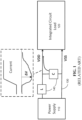
- FIG. 1 illustrates a block diagram of a printed circuit board (PCB) system that includes a power source 110 coupled to an integrated circuit (IC) load 120.
- the power source 110 provides power to the IC load 120 through PCB board traces 130 and components 140 such as inductance (L) and capacitance (C).
- the IC load 120 includes power-consuming electronics such as processor cores.
- the processor cores can generate current overloading that exceeds the maximum current limitation and cause damage to the PCB components and traces. As shown in the dashed block above the PCB system, the processor cores can also generate an inrush current in a short time that induces a voltage droop and causes system failure.
- a traditional method for suppressing current is using multiple capacitances and inductances. However, adding these components to the PCB board increases the total hardware size, thermal consumption, and cost.
- Another method is using software commands to decrease the power supply and operating frequency. However, software commands usually incur long latency and cannot suppress a current surge in time.
- a management circuit coupled to multiple processor cores for performing current suppression.
- the management circuit includes a detection circuit and a throttle signal generator.
- the detection circuit is operative to receive an activity signal from each processor core, and estimate a total current consumed by the plurality of processor cores based on activity signals.
- the activity signal indicates a current index proportional to current consumption of the processor core in a given time period.
- the throttle signal generator is operative to assert or de-assert throttle signals to the processor cores, one processor core at a time, based on one or more metrics calculated from the total current.
- a method for performing current suppression.
- the method comprises the steps of receiving an activity signal from each of a plurality of processor cores, and estimating a total current consumed by the plurality of processor cores based on activity signals.
- the activity signal indicates a current index proportional to current consumption of the processor core in a given time period.
- the method further comprises the step of asserting or de-asserting throttle signals to the plurality of processor cores, one processor core at a time, based on one or more metrics calculated from the total current.
- estimating the total current further comprises: estimating the total current by summing weighted current indices of all of the processor cores plus a leakage current, wherein each weighted current index is equal to the current index of each processor core multiplied by a current scaling factor and a dynamic voltage and frequency scaling (DVFS) factor.
- DVFS dynamic voltage and frequency scaling
- the method further comprises: initiating a trigger event transition when a peak current or an inrush current exceeds a high threshold to thereby ramp down the total current consumed by the processor cores.
- asserting or de-asserting throttle signals may further comprise: asserting the throttle signals to the processor cores, one processor core at a time with a programmable time interval between assertions of consecutive throttle signals.
- the method further comprises: initiating a release event transition when both a peak current and an inrush current are below a low threshold to thereby ramp up the total current consumed by the processor cores.
- asserting or de-asserting throttle signals may further comprise: de-asserting the throttle signals to the processor cores, one processor core at a time with a programmable time interval between de-assertions of consecutive throttle signals.
- Embodiments of the invention provide a mechanism for maximum current suppression (MCS) in a multi-core system to suppress peak current and/or inrush current for power integrity on a PCB board.
- the MCS can suppress the peak current to protect PCB board traces and components from physical damage.
- the MCS can also suppress the inrush current slew rate to prevent voltage droop and system failure.
- the MCS receives an activity signal from each processor core in the multi-core system and asserts or de-asserts a throttle signal accordingly. Based on the per-core activity signal, the MCS can detect a trigger event and use the throttle signal to reduce the activities of the cores.
- a “processor core” may be a central processing unit (CPU), a digital signal processor (DSP), a multimedia processor, a graphics processing unit (GPU), an artificial intelligence (AI) processor, a vector processor, or another general purpose or special purpose processing circuitry.
- a processor may be the same as a “core” or a “processor core”, while in some other systems a processor may include multiple cores.
- a multiprocessor system may also be known as a multi-core system.
- the term “core” is used interchangeably with the terms "processor” and "processor core.”
- FIG. 2 is a diagram 200 illustrating peak current suppression and inrush current suppression according to one embodiment.
- Diagram 200 shows a maximum current (IMAX) limitation line 210, which is the upper bound for the peak current.
- Diagram 200 also shows an inrush current limitation line 220, which is the upper bound for the change in current per time unit.
- the dotted line 250 is the current vs. time curve without the MCS
- the solid line 260 is the current vs. time curve with the MCS.
- the effect of the MCS on peak current suppression is indicated by the first arrow 230, and on inrush current suppression is indicated by the second arrow 240.
- the MCS can suppress the peak current to protect a PCB system from physical damage.
- the MCS can also suppress the inrush current slew rate to protect a PCB system from voltage droop and system failure.
- FIG. 3 is a block diagram illustrating a system 300 including an MCS management circuit 320 according to one embodiment.
- the system 300 includes processor cores (e.g., core_1 310a, core_2 310b, ...., core_N 310n), collectively referred to as processor cores 310, where index n can be any integer greater than one.
- the processor cores 310 may have the same processor type and/or different processor types.
- the processor cores 310 may share the same instruction set architecture (ISA) and/or different ISAs.
- ISA instruction set architecture
- system 300 can be integrated on a single integrated circuit die, or on separate dies in a multiple-circuit package. In one embodiment, the system 300 may be integrated as a system-on-a-chip (SOC). It is understood the embodiment of Figure 3 is simplified for illustration purposes. Additional hardware components may be included.
- SOC system-on-a-chip
- the system 300 further includes a memory.
- the memory may include on-chip and off-chip memory devices such as dynamic random access memory (DRAM), static RAM (SRAM), flash memory, and other volatile or non-volatile memory devices.
- the system 300 may also include a dynamic voltage frequency scaling (DVFS) controller to control the operating point (e.g., frequency and voltage) of the active computing circuits in the system 300.
- DRAM dynamic random access memory
- SRAM static RAM
- flash memory volatile or non-volatile memory devices.
- DVFS dynamic voltage frequency scaling
- the MCS management circuit 320 receives an activity signal and sends a throttle signal to each processor core 310.
- the activity signal indicates a current index estimated by each processor core 310, where the current index is proportional to the current consumption of the processor core 310 in a given time period.
- each operation code (OPCODE) of the processor core 310 is assigned a predetermined unit of activity. For example, the MOV operation can generate 11 units of activity, and the MUL operation can generate 55 units of activity.
- the number of units of activity is proportional to the current consumption by the OPCODE, for example, 100 units of activity may correspond to 200 milliamperes (mA) in current consumption, and 200 units of activity may correspond to 400 mA in current consumption.
- Each processor core 310 sums up the total units of activity in a given time period to generate a current index.
- the given time period may be a configurable time period.
- the OPCODEs that generate the total units of activity in a given time period may be the OPCODEs that are in the decode stage, in the execution stage, or have been recently executed by the corresponding processor core 310.
- the management circuit 320 receives an activity signal from each processor core 310 and calculates a total current and moving averages of the total current. Based on the total current and the moving averages, the management circuit 320 can detect both peak current and inrush current and assert or de-assert a throttle signal to each processor core. When the throttle signal to a processor core is asserted, the processor core can throttle its processing pipeline to reduce the activity and current consumption.
- FIG. 4 is a block diagram illustrating the MCS management circuit 320 ("management circuit 320") according to one embodiment.
- the management circuit 320 includes a total current generator 410, a moving average (MA) generator 420, a current detector 480, a finite state machine (FSM) 450, and a throttle signal generator 460.
- the current detector 480 includes a peak current detector (PCD) 430 for detecting the peak current generated or caused to be generated by the processor cores.
- the current detector 480 includes an inrush current detector (ICD) 440 for detecting the inrush current generated or caused to be generated by the processor cores.
- ICD inrush current detector
- the current detector 480 may include either PCD 430 or ICD 440, while in some other embodiments the current detector 480 may include both PCD 430 and ICD 440.
- Activity[n] is an 8-bit value and is the current index mentioned above in connection with Figure 3 .
- the number of bits may be different according to precision and cost considerations.
- Weight current scaling ⁇ DVFS scaling.
- the current scaling may be obtained by a linear regression method for improved precision.
- the moving average (MA) generator 420 generates moving averages of the total current.
- the moving averages may include 8MA, 32MA, 64MA, and the like.
- 8MA Average(TA[T], TA[T-1], ... TA[T-7])
- 32MA Average(8MA[T], 8MA[T-8], 8MA[T-16], 8MA[T-24]), where T is a timing cycle.
- Additional moving averages 64MA, 128MA, 256MA, 512MA, 1024MA, etc. can be generated in the same way as 32MA
- the peak current detector (PCD) 430 uses a short-term moving average (e.g. 32MA or another moving average) to detect the peak current. For each core, the PCD 430 compares the detected peak current with a high threshold (TH1h) to detect a PCD_Trigger event, and with a low threshold (TH1l) to detect a PCD_Release event. For example, the condition for the PCD_Trigger event is met when 32MA > TH1h, and the condition for the PCD_Release event is met when 32MA ⁇ TH1l, where TH1h and TH1l are programmable thresholds.
- TH1h high threshold
- TH1l low threshold
- the inrush current detection (ICD) 440 computes the difference between a short-term moving average and a long-term moving average, and uses the difference to detect the inrush current. For each core, the ICD 440 compares the difference with a high threshold (TH2h) to detect an ICD Trigger event, and with a low threshold (TH2l) to detect an ICD_Release event. For example, the difference may be computed as 32MA - 1024MA.
- the condition for the ICD Trigger event is met when (32MA - 1024MA) > TH2h, and the condition for the ICD Release event is met when (32MA - 1024MA) ⁇ TH2l, where TH2h and TH2l are programmable thresholds. It is noted that TH1h and TH2h may be different from each other, and TH1l and TH2l may be different from each other.
- Figure 5 is a diagram illustrating the relationship of total current and moving averages (e.g., 32MA and 1024MA) according to one embodiment.
- the total current is shown in a solid line
- 32MA is shown in a short-dashed line
- 1024MA is shown in a long-dashed line.
- FIG. 6 is a diagram of a finite state machine (FSM) 600 according to one embodiment.
- the FSM 600 is an example of the FSM 450 in Figure 4 .
- Idle state 610 indicates idleness; i.e., none of the processor cores in the system is being throttled.
- Ramp-down state 620 means ramping down the total current consumption of the processor cores from high to low current consumption.
- Ramp-up state 630 means ramping up the total current consumption of the processor cores from low to high current consumption.
- the FSM 600 undergoes state transitions in response to trigger events and release events. More specifically, the trigger event in the FSM 600 can be either PCD Trigger event or ICD Trigger event; that is, a trigger event transition can be initiated when the condition for either the PCD Trigger event or the ICD Trigger event is met. A trigger event transition can also be initiated when the conditions for both the PCD_Trigger event and the ICD Trigger event are met. A release event transition in the FSM 600 is initiated when the conditions for both the PCD_Release event and the ICD_Release event are met.
- the FSM 600 makes a transition to the ramp-down state 620 when receiving a trigger event to ramp down the total current consumption of the processor cores.
- the FSM 600 makes a transition to the ramp-up state 630 when receiving a release event to ramp up the total current consumption of the processor cores.
- FIG 7 is a diagram illustrating the timing waveform of throttle signals generated by the throttle signal generator 460 ( Figure 4 ) according to one embodiment.
- the system e.g., the system 300 in Figure 3
- the management circuit 320 ( Figure 4 ) initiates a trigger event transition. That is, the throttle signal generator 460 asserts the throttle signals to transition the system to the ramp-down state 620.
- the throttle signal is asserted to each processor core one by one, and there is a time interval between the assertions of consecutive throttle signals to prevent the system from voltage overshooting.
- the time interval is a programmable number; e.g., t1 nanoseconds (ns) where t1 >16.
- the management circuit 320 initiates a release event transition. That is, the throttle signal generator 460 de-asserts the throttle signals to transition the system to the ramp-up state 630.
- the throttle signal is de-asserted to each processor core one by one, and there is a time interval between the de-assertions of consecutive throttle signals to prevent the system from voltage undershooting.
- the time interval is a programmable number; e.g., t2 ns where t2 >32.
- the throttle signal generator 460 When the system is in the ramp-up state 630 and a trigger event is detected, the throttle signal generator 460 asserts the throttle signals to transition the system to the ramp-down state 620.
- the throttle signal is asserted to each processor core one by one as mentioned before.
- the system may transition from the ramp-up state 630 to the idle state 610 when no trigger event is detected.
- the management circuit 320 may detect that a condition for a trigger event is met before all of the processor cores are released from throttle. Upon the detection, the management circuit 320 asserts the throttle signals to those processor cores that are released in order to ramp down the total current. For example, the system may be in transition from the ramp-down state 620 to the ramp-up state 630, and only cores 1 and 2 (out of 3 cores) are released from throttle when a trigger event is detected. The management circuit 320 can re-assert throttle signals 1 and 2 to re-throttle cores 1 and 2 and the system re-enters the ramp-down state 620. In this example, throttle signal 3 remains asserted and core 3 stays throttled.
- the management circuit 320 may detect that a condition for a release event is met before all of the processor cores are throttled by the throttle signals. Upon the detection, the management circuit 320 de-asserts the throttle signals to those processor cores that are throttled in order to ramp up the total current.
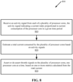
- FIG 8 is a flow diagram illustrating a method 800 for current suppression according to one embodiment.
- the method 800 may be performed by a circuit, such as the MCS management circuit 320 in Figures 3 and 4 .
- the operations of the MCS management circuit 320 may be performed by software instructions stored in a memory and executed by general-purpose or special-purpose processing hardware.
- the circuit is coupled to multiple processor cores, such as the cores 310 in Figure 3 .
- the circuit at step 810 receives an activity signal from each of the processor cores.
- the activity signal indicates a current index proportional to the current consumption of the processor core in a given time period.
- the circuit at step 820 estimates a total current consumed by the processor cores based on activity signals.
- the circuit at step 830 asserts or de-asserts throttle signals to the processor cores, one processor core at a time, based on one or more metrics calculated from the total current.
- the circuit further estimates a peak current and an inrush current consumed by the processor cores.
- the circuit may estimate the peak current by calculating a moving average of the total current, and assert or de-assert the throttle signals based on the peak current.
- the circuit may estimate the inrush current by calculating the difference between a short-term moving average and a long-term moving average of the total current, and assert or de-assert the throttle signals based on the inrush current.
- the circuit may estimate the total current by summing weighted current indices of all of the processor cores plus a leakage current, wherein each weighted current index is equal to the current index of each processor core multiplied by a current scaling factor and a DVFS factor.
- the circuit initiates a trigger event transition when the peak current or the inrush current exceeds a high threshold to thereby ramp down the total current consumed by the processor cores.
- the circuit asserts the throttle signals to the processor cores, one processor core at a time with a programmable time interval between the assertions of consecutive throttle signals.
- the circuit initiates a release event transition when both the peak current and the inrush current are below a low threshold to thereby ramp up the total current consumed by the processor cores.
- the circuit de-asserts the throttle signals to the processor cores, one processor core at a time with a programmable time interval between the de-assertions of consecutive throttle signals.
Landscapes
- Engineering & Computer Science (AREA)
- Theoretical Computer Science (AREA)
- Physics & Mathematics (AREA)
- General Engineering & Computer Science (AREA)
- General Physics & Mathematics (AREA)
- Power Engineering (AREA)
- Power Sources (AREA)
- Measurement Of Current Or Voltage (AREA)
- Emergency Protection Circuit Devices (AREA)
- Control Of Electrical Variables (AREA)
Abstract
Description
- This application claims the benefit of
U.S. Provisional Application No. 63/286,124 filed on December 6, 2021 - Embodiments of the invention relate to power management; more specifically, to current suppression in a multi-core system.
-
Figure 1 illustrates a block diagram of a printed circuit board (PCB) system that includes apower source 110 coupled to an integrated circuit (IC)load 120. Thepower source 110 provides power to theIC load 120 throughPCB board traces 130 andcomponents 140 such as inductance (L) and capacitance (C). TheIC load 120 includes power-consuming electronics such as processor cores. The processor cores can generate current overloading that exceeds the maximum current limitation and cause damage to the PCB components and traces. As shown in the dashed block above the PCB system, the processor cores can also generate an inrush current in a short time that induces a voltage droop and causes system failure. - A traditional method for suppressing current is using multiple capacitances and inductances. However, adding these components to the PCB board increases the total hardware size, thermal consumption, and cost. Another method is using software commands to decrease the power supply and operating frequency. However, software commands usually incur long latency and cannot suppress a current surge in time.
- Thus, there is a need for the improvement of power management in a processing system to ensure safe operations.
- In one embodiment, a management circuit coupled to multiple processor cores is provided for performing current suppression. The management circuit includes a detection circuit and a throttle signal generator. The detection circuit is operative to receive an activity signal from each processor core, and estimate a total current consumed by the plurality of processor cores based on activity signals. The activity signal indicates a current index proportional to current consumption of the processor core in a given time period. The throttle signal generator is operative to assert or de-assert throttle signals to the processor cores, one processor core at a time, based on one or more metrics calculated from the total current.
- In another embodiment, a method is provided for performing current suppression. The method comprises the steps of receiving an activity signal from each of a plurality of processor cores, and estimating a total current consumed by the plurality of processor cores based on activity signals. The activity signal indicates a current index proportional to current consumption of the processor core in a given time period. The method further comprises the step of asserting or de-asserting throttle signals to the plurality of processor cores, one processor core at a time, based on one or more metrics calculated from the total current.
- In one arrangement of the method, estimating the total current further comprises: estimating the total current by summing weighted current indices of all of the processor cores plus a leakage current, wherein each weighted current index is equal to the current index of each processor core multiplied by a current scaling factor and a dynamic voltage and frequency scaling (DVFS) factor.
- In another arrangement of the method, the method further comprises: initiating a trigger event transition when a peak current or an inrush current exceeds a high threshold to thereby ramp down the total current consumed by the processor cores. In this arrangement, asserting or de-asserting throttle signals may further comprise: asserting the throttle signals to the processor cores, one processor core at a time with a programmable time interval between assertions of consecutive throttle signals.
- In another arrangement of the method, the method, further comprises: initiating a release event transition when both a peak current and an inrush current are below a low threshold to thereby ramp up the total current consumed by the processor cores. In this arrangement, asserting or de-asserting throttle signals may further comprise: de-asserting the throttle signals to the processor cores, one processor core at a time with a programmable time interval between de-assertions of consecutive throttle signals.
- Other aspects and features will become apparent to those ordinarily skilled in the art upon review of the following description of specific embodiments in conjunction with the accompanying figures.
- The present invention is illustrated by way of example, and not by way of limitation, in the figures of the accompanying drawings in which like references indicate similar elements. It should be noted that different references to "an" or "one" embodiment in this disclosure are not necessarily to the same embodiment, and such references mean at least one. Further, when a particular feature, structure, or characteristic is described in connection with an embodiment, it is submitted that it is within the knowledge of one skilled in the art to effect such feature, structure, or characteristic in connection with other embodiments whether or not explicitly described.
-
Figure 1 is a block diagram of a printed circuit board (PCB) system in the related art. -
Figure 2 is a diagram illustrating peak current suppression and inrush current suppression according to one embodiment. -
Figure 3 is a block diagram illustrating a system including a maximum current suppression (MCS) management circuit according to one embodiment. -
Figure 4 is a block diagram illustrating an MCS management circuit according to one embodiment. -
Figure 5 is a diagram illustrating a relationship between total current and moving averages according to one embodiment. -
Figure 6 is a diagram of a finite state machine (FSM) according to one embodiment. -
Figure 7 is a diagram illustrating a timing waveform of throttle signals according to one embodiment. -
Figure 8 is a flow diagram illustrating a method for current suppression according to one embodiment. - In the following description, numerous specific details are set forth. However, it is understood that embodiments of the invention may be practiced without these specific details. In other instances, well-known circuits, structures, and techniques have not been shown in detail in order not to obscure the understanding of this description. It will be appreciated, however, by one skilled in the art, that the invention may be practiced without such specific details. Those of ordinary skill in the art, with the included descriptions, will be able to implement appropriate functionality without undue experimentation.
- Embodiments of the invention provide a mechanism for maximum current suppression (MCS) in a multi-core system to suppress peak current and/or inrush current for power integrity on a PCB board. The MCS can suppress the peak current to protect PCB board traces and components from physical damage. The MCS can also suppress the inrush current slew rate to prevent voltage droop and system failure. In one embodiment, the MCS receives an activity signal from each processor core in the multi-core system and asserts or de-asserts a throttle signal accordingly. Based on the per-core activity signal, the MCS can detect a trigger event and use the throttle signal to reduce the activities of the cores.
- In the system described herein, a "processor core" may be a central processing unit (CPU), a digital signal processor (DSP), a multimedia processor, a graphics processing unit (GPU), an artificial intelligence (AI) processor, a vector processor, or another general purpose or special purpose processing circuitry. In some systems, a processor may be the same as a "core" or a "processor core", while in some other systems a processor may include multiple cores. A multiprocessor system may also be known as a multi-core system. In the system described herein, the term "core" is used interchangeably with the terms "processor" and "processor core."
-
Figure 2 is a diagram 200 illustrating peak current suppression and inrush current suppression according to one embodiment. Diagram 200 shows a maximum current (IMAX)limitation line 210, which is the upper bound for the peak current. Diagram 200 also shows an inrush current limitation line 220, which is the upper bound for the change in current per time unit. Thedotted line 250 is the current vs. time curve without the MCS, and thesolid line 260 is the current vs. time curve with the MCS. The effect of the MCS on peak current suppression is indicated by thefirst arrow 230, and on inrush current suppression is indicated by thesecond arrow 240. Thus, the MCS can suppress the peak current to protect a PCB system from physical damage. The MCS can also suppress the inrush current slew rate to protect a PCB system from voltage droop and system failure. -
Figure 3 is a block diagram illustrating asystem 300 including anMCS management circuit 320 according to one embodiment. Thesystem 300 includes processor cores (e.g., core_1 310a,core_2 310b, ....,core_N 310n), collectively referred to as processor cores 310, where index n can be any integer greater than one. The processor cores 310 may have the same processor type and/or different processor types. The processor cores 310 may share the same instruction set architecture (ISA) and/or different ISAs. - In one embodiment, the
system 300 can be integrated on a single integrated circuit die, or on separate dies in a multiple-circuit package. In one embodiment, thesystem 300 may be integrated as a system-on-a-chip (SOC). It is understood the embodiment ofFigure 3 is simplified for illustration purposes. Additional hardware components may be included. - Although not shown in
Figure 3 , thesystem 300 further includes a memory. The memory may include on-chip and off-chip memory devices such as dynamic random access memory (DRAM), static RAM (SRAM), flash memory, and other volatile or non-volatile memory devices. Thesystem 300 may also include a dynamic voltage frequency scaling (DVFS) controller to control the operating point (e.g., frequency and voltage) of the active computing circuits in thesystem 300. - In one embodiment, the MCS management circuit 320 (also referred to as the management circuit 320) receives an activity signal and sends a throttle signal to each processor core 310. The activity signal indicates a current index estimated by each processor core 310, where the current index is proportional to the current consumption of the processor core 310 in a given time period. In one embodiment, each operation code (OPCODE) of the processor core 310 is assigned a predetermined unit of activity. For example, the MOV operation can generate 11 units of activity, and the MUL operation can generate 55 units of activity. The number of units of activity is proportional to the current consumption by the OPCODE, for example, 100 units of activity may correspond to 200 milliamperes (mA) in current consumption, and 200 units of activity may correspond to 400 mA in current consumption. Each processor core 310 sums up the total units of activity in a given time period to generate a current index. The given time period may be a configurable time period. The OPCODEs that generate the total units of activity in a given time period may be the OPCODEs that are in the decode stage, in the execution stage, or have been recently executed by the corresponding processor core 310.
- The
management circuit 320 receives an activity signal from each processor core 310 and calculates a total current and moving averages of the total current. Based on the total current and the moving averages, themanagement circuit 320 can detect both peak current and inrush current and assert or de-assert a throttle signal to each processor core. When the throttle signal to a processor core is asserted, the processor core can throttle its processing pipeline to reduce the activity and current consumption. -
Figure 4 is a block diagram illustrating the MCS management circuit 320 ("management circuit 320") according to one embodiment. Themanagement circuit 320 includes a totalcurrent generator 410, a moving average (MA)generator 420, acurrent detector 480, a finite state machine (FSM) 450, and athrottle signal generator 460. In one embodiment, thecurrent detector 480 includes a peak current detector (PCD) 430 for detecting the peak current generated or caused to be generated by the processor cores. In one embodiment, thecurrent detector 480 includes an inrush current detector (ICD) 440 for detecting the inrush current generated or caused to be generated by the processor cores. Although bothPCD 430 and ICD 440 are shown inFigure 4 , in some embodiments thecurrent detector 480 may include eitherPCD 430 or ICD 440, while in some other embodiments thecurrent detector 480 may include bothPCD 430 and ICD 440. - The total
current generator 410 uses scaling and summation to calculate a total current value, where the total current = Summation of (Activity[n] × Weight) + Leakage_current, n is a running index identifyingprocessor core 1, ...., N. In an embodiment where an 8-bit bus is used to carry each activity signal, Activity[n] is an 8-bit value and is the current index mentioned above in connection withFigure 3 . The number of bits may be different according to precision and cost considerations. - In one embodiment, Weight = current scaling × DVFS scaling. In one embodiment, current scaling = IMAX.Dyn(mA)/[8'hFF], where IMAX.Dyn(mA) is the maximum average dynamic current in milliampere (mA). For example, if IMAX.Dyn(mA) = 4000 mA and Activity[n] is 8-bit, current scaling = 4000/255 = 15.7. In an alternative embodiment, the current scaling may be obtained by a linear regression method for improved precision.
- In one embodiment, DVFS scaling = (Vcur × Fcur)/(Vmax × Fmax). For example, when Vcur = 0.7 volts, Fcur = 0.9 GHz, Vmax = 0.75 volts, Fmax = 1 GHz, DVFS scaling = 0.84. Thus, in this example, Weight = current scaling × DVFS scaling = 15.7 × 0.84 = 13.2.
- The moving average (MA)
generator 420 generates moving averages of the total current. As an example, the moving averages may include 8MA, 32MA, 64MA, and the like. For example, 8MA = Average(TA[T], TA[T-1], ... TA[T-7]), and 32MA = Average(8MA[T], 8MA[T-8], 8MA[T-16], 8MA[T-24]), where T is a timing cycle. Additional moving averages 64MA, 128MA, 256MA, 512MA, 1024MA, etc. can be generated in the same way as 32MA - In one embodiment, the peak current detector (PCD) 430 uses a short-term moving average (e.g. 32MA or another moving average) to detect the peak current. For each core, the
PCD 430 compares the detected peak current with a high threshold (TH1h) to detect a PCD_Trigger event, and with a low threshold (TH1l) to detect a PCD_Release event. For example, the condition for the PCD_Trigger event is met when 32MA > TH1h, and the condition for the PCD_Release event is met when 32MA < TH1l, where TH1h and TH1l are programmable thresholds. - In one embodiment, the inrush current detection (ICD) 440 computes the difference between a short-term moving average and a long-term moving average, and uses the difference to detect the inrush current. For each core, the ICD 440 compares the difference with a high threshold (TH2h) to detect an ICD Trigger event, and with a low threshold (TH2l) to detect an ICD_Release event. For example, the difference may be computed as 32MA - 1024MA. In one embodiment, the condition for the ICD Trigger event is met when (32MA - 1024MA) > TH2h, and the condition for the ICD Release event is met when (32MA - 1024MA) < TH2l, where TH2h and TH2l are programmable thresholds. It is noted that TH1h and TH2h may be different from each other, and TH1l and TH2l may be different from each other.
-
Figure 5 is a diagram illustrating the relationship of total current and moving averages (e.g., 32MA and 1024MA) according to one embodiment. The total current is shown in a solid line, 32MA is shown in a short-dashed line, and 1024MA is shown in a long-dashed line. -
Figure 6 is a diagram of a finite state machine (FSM) 600 according to one embodiment. TheFSM 600 is an example of theFSM 450 inFigure 4 . There are three states in the FSM 600: anidle state 610, a ramp-downstate 620, and a ramp-upstate 630.Idle state 610 indicates idleness; i.e., none of the processor cores in the system is being throttled. Ramp-downstate 620 means ramping down the total current consumption of the processor cores from high to low current consumption. Ramp-upstate 630 means ramping up the total current consumption of the processor cores from low to high current consumption. - The
FSM 600 undergoes state transitions in response to trigger events and release events. More specifically, the trigger event in theFSM 600 can be either PCD Trigger event or ICD Trigger event; that is, a trigger event transition can be initiated when the condition for either the PCD Trigger event or the ICD Trigger event is met. A trigger event transition can also be initiated when the conditions for both the PCD_Trigger event and the ICD Trigger event are met. A release event transition in theFSM 600 is initiated when the conditions for both the PCD_Release event and the ICD_Release event are met. - The
FSM 600 makes a transition to the ramp-downstate 620 when receiving a trigger event to ramp down the total current consumption of the processor cores. TheFSM 600 makes a transition to the ramp-upstate 630 when receiving a release event to ramp up the total current consumption of the processor cores. -
Figure 7 is a diagram illustrating the timing waveform of throttle signals generated by the throttle signal generator 460 (Figure 4 ) according to one embodiment. Referring also toFigures 3, 4 , and6 , the system (e.g., thesystem 300 inFigure 3 ) is initially in theidle state 610. When a trigger event is detected (e.g., when a condition for either PCD Trigger event or ICD Trigger event is met), the management circuit 320 (Figure 4 ) initiates a trigger event transition. That is, thethrottle signal generator 460 asserts the throttle signals to transition the system to the ramp-downstate 620. The throttle signal is asserted to each processor core one by one, and there is a time interval between the assertions of consecutive throttle signals to prevent the system from voltage overshooting. The time interval is a programmable number; e.g., t1 nanoseconds (ns) where t1 >16. - When the system is in the ramp-down
state 620 and a release event is detected (e.g., when conditions for both PCD Release event and ICD Release event are met), themanagement circuit 320 initiates a release event transition. That is, thethrottle signal generator 460 de-asserts the throttle signals to transition the system to the ramp-upstate 630. The throttle signal is de-asserted to each processor core one by one, and there is a time interval between the de-assertions of consecutive throttle signals to prevent the system from voltage undershooting. The time interval is a programmable number; e.g., t2 ns where t2 >32. - When the system is in the ramp-up
state 630 and a trigger event is detected, thethrottle signal generator 460 asserts the throttle signals to transition the system to the ramp-downstate 620. The throttle signal is asserted to each processor core one by one as mentioned before. Alternatively, the system may transition from the ramp-upstate 630 to theidle state 610 when no trigger event is detected. - When the system is in transition from the ramp-down
state 620 to the ramp-upstate 630, themanagement circuit 320 may detect that a condition for a trigger event is met before all of the processor cores are released from throttle. Upon the detection, themanagement circuit 320 asserts the throttle signals to those processor cores that are released in order to ramp down the total current. For example, the system may be in transition from the ramp-downstate 620 to the ramp-upstate 630, and onlycores 1 and 2 (out of 3 cores) are released from throttle when a trigger event is detected. Themanagement circuit 320 can re-assertthrottle signals re-throttle cores state 620. In this example, throttle signal 3 remains asserted and core 3 stays throttled. - Similarly, when the system is in transition from the ramp-up
state 630 to the ramp-downstate 620, themanagement circuit 320 may detect that a condition for a release event is met before all of the processor cores are throttled by the throttle signals. Upon the detection, themanagement circuit 320 de-asserts the throttle signals to those processor cores that are throttled in order to ramp up the total current. -
Figure 8 is a flow diagram illustrating amethod 800 for current suppression according to one embodiment. Themethod 800 may be performed by a circuit, such as theMCS management circuit 320 inFigures 3 and 4 . In an alternative embodiment, the operations of theMCS management circuit 320 may be performed by software instructions stored in a memory and executed by general-purpose or special-purpose processing hardware. The circuit is coupled to multiple processor cores, such as the cores 310 inFigure 3 . - The circuit at
step 810 receives an activity signal from each of the processor cores. The activity signal indicates a current index proportional to the current consumption of the processor core in a given time period. The circuit atstep 820 estimates a total current consumed by the processor cores based on activity signals. The circuit atstep 830 asserts or de-asserts throttle signals to the processor cores, one processor core at a time, based on one or more metrics calculated from the total current. - In one embodiment, the circuit further estimates a peak current and an inrush current consumed by the processor cores. The circuit may estimate the peak current by calculating a moving average of the total current, and assert or de-assert the throttle signals based on the peak current. The circuit may estimate the inrush current by calculating the difference between a short-term moving average and a long-term moving average of the total current, and assert or de-assert the throttle signals based on the inrush current. The circuit may estimate the total current by summing weighted current indices of all of the processor cores plus a leakage current, wherein each weighted current index is equal to the current index of each processor core multiplied by a current scaling factor and a DVFS factor.
- In one embodiment, the circuit initiates a trigger event transition when the peak current or the inrush current exceeds a high threshold to thereby ramp down the total current consumed by the processor cores. When the trigger event transition is initiated, the circuit asserts the throttle signals to the processor cores, one processor core at a time with a programmable time interval between the assertions of consecutive throttle signals. The circuit initiates a release event transition when both the peak current and the inrush current are below a low threshold to thereby ramp up the total current consumed by the processor cores. When the release event transition is initiated, the circuit de-asserts the throttle signals to the processor cores, one processor core at a time with a programmable time interval between the de-assertions of consecutive throttle signals.
- The operations of the flow diagram of
Figure 8 have been described with reference to the exemplary embodiments ofFigures 3 and 4 . However, it should be understood that the operations of the flow diagram ofFigure 8 can be performed by embodiments of the invention other than the embodiments ofFigures 3 and 4 , and the embodiments ofFigures 3 and 4 can perform operations different than those discussed with reference to the flow diagram. While the flow diagram ofFigure 8 shows a particular order of operations performed by certain embodiments of the invention, it should be understood that such order is exemplary (e.g., alternative embodiments may perform the operations in a different order, combine certain operations, overlap certain operations, etc.). - Various functional components, blocks, or modules have been described herein. As will be appreciated by persons skilled in the art, the functional blocks or modules may be implemented through circuits (either dedicated circuits or general-purpose circuits, which operate under the control of one or more processors and coded instructions), which will typically comprise transistors that are configured in such a way as to control the operation of the circuity in accordance with the functions and operations described herein.
- While the invention has been described in terms of several embodiments, those skilled in the art will recognize that the invention is not limited to the embodiments described, and can be practiced with modification and alteration within the spirit and scope of the appended claims. The description is thus to be regarded as illustrative instead of limiting.
Claims (15)
- A management circuit coupled to a plurality of processor cores for performing current suppression, comprising:a detection circuit operative to:receive an activity signal from each processor core, the activity signal indicating a current index proportional to current consumption of the processor core in a given time period; andestimate a total current consumed by the plurality of processor cores based on activity signals; anda throttle signal generator operative to assert or de-assert throttle signals to the plurality of processor cores, one processor core at a time, based on one or more metrics calculated from the total current.
- The management circuit of claim 1, wherein the detection circuit is further operative to estimate a peak current and an inrush current consumed by the plurality of processor cores.
- The management circuit of claim 1, wherein the management circuit is further operative to:estimate a peak current of the processor cores by calculating a moving average of the total current; andassert or de-assert the throttle signals based on the peak current.
- The management circuit of claim 1, wherein the management circuit is further operative to:estimate an inrush current of the processor cores by calculating a difference between a short-term moving average and a long-term moving average of the total current; andassert or de-assert throttle signals based on the inrush current.
- The management circuit of any one of the preceding claims, wherein the detection circuit is further operative to:
estimate the total current by summing weighted current indices of all of the processor cores plus a leakage current, wherein each weighted current index is equal to the current index of each processor core multiplied by a current scaling factor and a dynamic voltage and frequency scaling (DVFS) factor. - The management circuit of any one of the preceding claims, further comprising:
a finite state machine (FSM), according to which the management circuit initiates a trigger event transition when a peak current or an inrush current exceeds a high threshold to thereby ramp down the total current consumed by the processor cores. - The management circuit of claim 6, wherein the throttle signal generator is further operative to:
assert the throttle signals to the processor cores, one processor core at a time with a programmable time interval between assertions of consecutive throttle signals. - The management circuit of any one of claims 1 to 5, further comprising:
a finite state machine (FSM), according to which the management circuit initiates a release event transition when both a peak current and an inrush current are below a low threshold to thereby ramp up the total current consumed by the processor cores. - The management circuit of claim 8, wherein the throttle signal generator is further operative to:
de-assert the throttle signals to the processor cores, one processor core at a time with a programmable time interval between de-assertions of consecutive throttle signals. - The management circuit of any one of the preceding claims, wherein the management circuit is further operative to:detect that a condition for a release event is met before all of the processor cores are throttled by the throttle signals; andde-assert the throttle signals to the processor cores that are throttled to thereby ramp up the total current.
- The management circuit of any one of claims 1 to 9, wherein the management circuit is further operative to:detect that a condition for a trigger event is met before all of the processor cores are released from throttle; andassert the throttle signals to the processor cores that are released to thereby ramp down the total current.
- A method for performing current suppression, comprising:receiving an activity signal from each of a plurality of processor cores, the activity signal indicating a current index proportional to current consumption of the processor core in a given time period; andestimating a total current consumed by the plurality of processor cores based on activity signals; andasserting or de-asserting throttle signals to the plurality of processor cores, one processor core at a time, based on one or more metrics calculated from the total current.
- The method of claim 12, wherein estimating the total current further comprises:
estimating a peak current and an inrush current consumed by the plurality of processor cores. - The method of claim 12, further comprising:estimating a peak current of the processor cores by calculating a moving average of the total current; andasserting or de-asserting the throttle signals based on the peak current.
- The method of claim 12, further comprising:estimating an inrush current of the processor cores by calculating a difference between a short-term moving average and a long-term moving average of the total current; andasserting or de-asserting throttle signals based on the inrush current.
Applications Claiming Priority (2)
| Application Number | Priority Date | Filing Date | Title |
|---|---|---|---|
| US202163286124P | 2021-12-06 | 2021-12-06 | |
| US17/866,483 US11989077B2 (en) | 2021-12-06 | 2022-07-16 | Maximum current suppression for power management in a multi-core system |
Publications (1)
| Publication Number | Publication Date |
|---|---|
| EP4191381A1 true EP4191381A1 (en) | 2023-06-07 |
Family
ID=84389367
Family Applications (1)
| Application Number | Title | Priority Date | Filing Date |
|---|---|---|---|
| EP22211364.9A Pending EP4191381A1 (en) | 2021-12-06 | 2022-12-05 | Maximum current suppression for power management in a multi-core system |
Country Status (4)
| Country | Link |
|---|---|
| US (1) | US11989077B2 (en) |
| EP (1) | EP4191381A1 (en) |
| CN (1) | CN116231777A (en) |
| TW (1) | TWI817741B (en) |
Cited By (1)
| Publication number | Priority date | Publication date | Assignee | Title |
|---|---|---|---|---|
| WO2025170687A1 (en) * | 2024-02-06 | 2025-08-14 | Qualcomm Incorporated | System peak current management for mobile devices |
Families Citing this family (2)
| Publication number | Priority date | Publication date | Assignee | Title |
|---|---|---|---|---|
| US12061509B2 (en) * | 2022-12-15 | 2024-08-13 | International Business Machines Corporation | Voltage droop and overshoot management using non-linear slope detection |
| US12332711B2 (en) * | 2023-03-24 | 2025-06-17 | Qualcomm Incorporated | Systems and methods for mitigating peak current and improving overall performance |
Citations (4)
| Publication number | Priority date | Publication date | Assignee | Title |
|---|---|---|---|---|
| US20120254641A1 (en) * | 2011-03-31 | 2012-10-04 | Efraim Rotem | Apparatus and method for high current protection |
| US20150309551A1 (en) * | 2014-04-29 | 2015-10-29 | Qualcomm Incorporated | Systems and methods for providing local hardware limit management and enforcement |
| US20200257349A1 (en) * | 2019-02-07 | 2020-08-13 | International Business Machines Corporation | Multi-layered processor throttle controller |
| US20210096635A1 (en) * | 2019-09-27 | 2021-04-01 | Qualcomm Incorporated | Power control based on performance modification through pulse modulation |
Family Cites Families (19)
| Publication number | Priority date | Publication date | Assignee | Title |
|---|---|---|---|---|
| US6564328B1 (en) * | 1999-12-23 | 2003-05-13 | Intel Corporation | Microprocessor with digital power throttle |
| US7584372B2 (en) * | 2006-04-25 | 2009-09-01 | Mediatek Inc. | Station control method and station using the same |
| US8942932B2 (en) * | 2010-08-31 | 2015-01-27 | Advanced Micro Devices, Inc. | Determining transistor leakage for an integrated circuit |
| US9069555B2 (en) * | 2011-03-21 | 2015-06-30 | Intel Corporation | Managing power consumption in a multi-core processor |
| US8650428B2 (en) * | 2011-07-19 | 2014-02-11 | Ati Technologies Ulc | Dynamic weight calculation in a digital power estimation and management system |
| US9753520B2 (en) * | 2013-12-23 | 2017-09-05 | Dell Products, L.P. | Predictive power capping and power allocation to computing nodes in a rack-based information handling system |
| US9507405B2 (en) * | 2014-06-18 | 2016-11-29 | Oracle International Corporation | System and method for managing power in a chip multiprocessor using a proportional feedback mechanism |
| GB2530782A (en) * | 2014-10-02 | 2016-04-06 | Ibm | Voltage droop reduction in a processor |
| US20170168541A1 (en) * | 2015-12-15 | 2017-06-15 | Intel Corporation | Processor core energy management |
| US20190146567A1 (en) * | 2017-11-10 | 2019-05-16 | Advanced Micro Devices, Inc. | Processor throttling based on accumulated combined current measurements |
| US11543878B2 (en) * | 2018-05-01 | 2023-01-03 | Intel Corporation | Power control arbitration |
| US11099628B2 (en) * | 2018-09-27 | 2021-08-24 | Intel Corporation | Throttling of components using priority ordering |
| US11429173B2 (en) * | 2018-12-21 | 2022-08-30 | Intel Corporation | Apparatus and method for proactive power management to avoid unintentional processor shutdown |
| US11409560B2 (en) * | 2019-03-28 | 2022-08-09 | Intel Corporation | System, apparatus and method for power license control of a processor |
| US12124350B2 (en) * | 2020-04-28 | 2024-10-22 | Intel Corporation | Real-time power meter for optimizing processor power management |
| US12124314B2 (en) * | 2021-03-19 | 2024-10-22 | Intel Corporation | Apparatus and method to detect power supply security attack and risk mitigation |
| US11625087B2 (en) * | 2021-08-28 | 2023-04-11 | International Business Machines Corporation | Current prediction-based instruction throttling control |
| US11966786B2 (en) * | 2021-08-28 | 2024-04-23 | International Business Machines Corporation | Proxy-based instruction throttling control |
| US11831159B2 (en) * | 2022-01-25 | 2023-11-28 | Infineon Technologies Ag | Systems, devices and methods for power management and power estimation |
-
2022
- 2022-07-16 US US17/866,483 patent/US11989077B2/en active Active
- 2022-09-27 TW TW111136541A patent/TWI817741B/en active
- 2022-10-10 CN CN202211238050.4A patent/CN116231777A/en active Pending
- 2022-12-05 EP EP22211364.9A patent/EP4191381A1/en active Pending
Patent Citations (4)
| Publication number | Priority date | Publication date | Assignee | Title |
|---|---|---|---|---|
| US20120254641A1 (en) * | 2011-03-31 | 2012-10-04 | Efraim Rotem | Apparatus and method for high current protection |
| US20150309551A1 (en) * | 2014-04-29 | 2015-10-29 | Qualcomm Incorporated | Systems and methods for providing local hardware limit management and enforcement |
| US20200257349A1 (en) * | 2019-02-07 | 2020-08-13 | International Business Machines Corporation | Multi-layered processor throttle controller |
| US20210096635A1 (en) * | 2019-09-27 | 2021-04-01 | Qualcomm Incorporated | Power control based on performance modification through pulse modulation |
Cited By (1)
| Publication number | Priority date | Publication date | Assignee | Title |
|---|---|---|---|---|
| WO2025170687A1 (en) * | 2024-02-06 | 2025-08-14 | Qualcomm Incorporated | System peak current management for mobile devices |
Also Published As
| Publication number | Publication date |
|---|---|
| TWI817741B (en) | 2023-10-01 |
| CN116231777A (en) | 2023-06-06 |
| TW202324035A (en) | 2023-06-16 |
| US11989077B2 (en) | 2024-05-21 |
| US20230176645A1 (en) | 2023-06-08 |
Similar Documents
| Publication | Publication Date | Title |
|---|---|---|
| EP4191381A1 (en) | Maximum current suppression for power management in a multi-core system | |
| US9106136B2 (en) | Pulse width modulation load share bus | |
| US20100264741A1 (en) | Adaptation of an active power supply set using an event trigger | |
| US11449127B2 (en) | Peak power determination for an integrated circuit device | |
| CN104781751B (en) | Method and apparatus for managing computing system power | |
| CN110658903A (en) | Method and apparatus for power resource protection | |
| US20130283083A1 (en) | Maintaining operational stability on a system on a chip | |
| US9575529B2 (en) | Voltage droop reduction in a processor | |
| US20130219206A1 (en) | Method And Apparatus For Reducing Server Power Supply Size And Cost | |
| US20120144221A1 (en) | Load step mitigation method and apparatus | |
| US20190146567A1 (en) | Processor throttling based on accumulated combined current measurements | |
| US20160132096A1 (en) | System and method for controlling idle state exits to manage di/dt issues | |
| US10152106B2 (en) | Power excursion tolerant power system | |
| US8782444B2 (en) | Circuit protection system and method for a circuit utilizing chip type power supply | |
| US20140115361A1 (en) | Load step management | |
| US12228954B2 (en) | Voltage regulator wake-up | |
| US8826056B2 (en) | Circuit protection system and method | |
| Floyd et al. | Voltage droop reduction using throttling controlled by timing margin feedback | |
| US10754410B2 (en) | System and method for standby mode operation of power management system | |
| US9785218B2 (en) | Performance state selection for low activity scenarios | |
| US12424933B2 (en) | Power consumption control of an electronic system and apparatus for controlling the power consumption | |
| US20250112470A1 (en) | Detection of low efficiency power states | |
| US20250044846A1 (en) | Apparatus, method, device and system for power transmission based on psys, and medium | |
| US9952564B2 (en) | Circuit arrangement and method for controlling the operation of a plurality of components requiring a supply in a circuit arrangement | |
| Hsieh et al. | In-situ self-aware adaptive power control system with multi-mode power gating network |
Legal Events
| Date | Code | Title | Description |
|---|---|---|---|
| PUAI | Public reference made under article 153(3) epc to a published international application that has entered the european phase |
Free format text: ORIGINAL CODE: 0009012 |
|
| STAA | Information on the status of an ep patent application or granted ep patent |
Free format text: STATUS: THE APPLICATION HAS BEEN PUBLISHED |
|
| AK | Designated contracting states |
Kind code of ref document: A1 Designated state(s): AL AT BE BG CH CY CZ DE DK EE ES FI FR GB GR HR HU IE IS IT LI LT LU LV MC ME MK MT NL NO PL PT RO RS SE SI SK SM TR |
|
| STAA | Information on the status of an ep patent application or granted ep patent |
Free format text: STATUS: REQUEST FOR EXAMINATION WAS MADE |
|
| 17P | Request for examination filed |
Effective date: 20231207 |
|
| RBV | Designated contracting states (corrected) |
Designated state(s): AL AT BE BG CH CY CZ DE DK EE ES FI FR GB GR HR HU IE IS IT LI LT LU LV MC ME MK MT NL NO PL PT RO RS SE SI SK SM TR |
|
| STAA | Information on the status of an ep patent application or granted ep patent |
Free format text: STATUS: EXAMINATION IS IN PROGRESS |
|
| 17Q | First examination report despatched |
Effective date: 20250605 |