EP4191308A1 - High-speed active contact - Google Patents
High-speed active contact Download PDFInfo
- Publication number
- EP4191308A1 EP4191308A1 EP22210618.9A EP22210618A EP4191308A1 EP 4191308 A1 EP4191308 A1 EP 4191308A1 EP 22210618 A EP22210618 A EP 22210618A EP 4191308 A1 EP4191308 A1 EP 4191308A1
- Authority
- EP
- European Patent Office
- Prior art keywords
- connector
- contact
- circuit board
- circuitry
- housing
- Prior art date
- Legal status (The legal status is an assumption and is not a legal conclusion. Google has not performed a legal analysis and makes no representation as to the accuracy of the status listed.)
- Pending
Links
Images




Classifications
-
- G—PHYSICS
- G02—OPTICS
- G02B—OPTICAL ELEMENTS, SYSTEMS OR APPARATUS
- G02B6/00—Light guides; Structural details of arrangements comprising light guides and other optical elements, e.g. couplings
- G02B6/24—Coupling light guides
- G02B6/42—Coupling light guides with opto-electronic elements
- G02B6/4201—Packages, e.g. shape, construction, internal or external details
- G02B6/4274—Electrical aspects
- G02B6/428—Electrical aspects containing printed circuit boards [PCB]
-
- G—PHYSICS
- G02—OPTICS
- G02B—OPTICAL ELEMENTS, SYSTEMS OR APPARATUS
- G02B6/00—Light guides; Structural details of arrangements comprising light guides and other optical elements, e.g. couplings
- G02B6/24—Coupling light guides
- G02B6/42—Coupling light guides with opto-electronic elements
- G02B6/4292—Coupling light guides with opto-electronic elements the light guide being disconnectable from the opto-electronic element, e.g. mutually self aligning arrangements
-
- G—PHYSICS
- G02—OPTICS
- G02B—OPTICAL ELEMENTS, SYSTEMS OR APPARATUS
- G02B6/00—Light guides; Structural details of arrangements comprising light guides and other optical elements, e.g. couplings
- G02B6/24—Coupling light guides
- G02B6/36—Mechanical coupling means
- G02B6/38—Mechanical coupling means having fibre to fibre mating means
- G02B6/3807—Dismountable connectors, i.e. comprising plugs
- G02B6/3873—Connectors using guide surfaces for aligning ferrule ends, e.g. tubes, sleeves, V-grooves, rods, pins, balls
- G02B6/3874—Connectors using guide surfaces for aligning ferrule ends, e.g. tubes, sleeves, V-grooves, rods, pins, balls using tubes, sleeves to align ferrules
- G02B6/3878—Connectors using guide surfaces for aligning ferrule ends, e.g. tubes, sleeves, V-grooves, rods, pins, balls using tubes, sleeves to align ferrules comprising a plurality of ferrules, branching and break-out means
-
- G—PHYSICS
- G02—OPTICS
- G02B—OPTICAL ELEMENTS, SYSTEMS OR APPARATUS
- G02B6/00—Light guides; Structural details of arrangements comprising light guides and other optical elements, e.g. couplings
- G02B6/24—Coupling light guides
- G02B6/42—Coupling light guides with opto-electronic elements
- G02B6/4201—Packages, e.g. shape, construction, internal or external details
- G02B6/4274—Electrical aspects
- G02B6/4284—Electrical aspects of optical modules with disconnectable electrical connectors
-
- H—ELECTRICITY
- H01—ELECTRIC ELEMENTS
- H01R—ELECTRICALLY-CONDUCTIVE CONNECTIONS; STRUCTURAL ASSOCIATIONS OF A PLURALITY OF MUTUALLY-INSULATED ELECTRICAL CONNECTING ELEMENTS; COUPLING DEVICES; CURRENT COLLECTORS
- H01R13/00—Details of coupling devices of the kinds covered by groups H01R12/70 or H01R24/00 - H01R33/00
- H01R13/66—Structural association with built-in electrical component
- H01R13/665—Structural association with built-in electrical component with built-in electronic circuit
- H01R13/6658—Structural association with built-in electrical component with built-in electronic circuit on printed circuit board
-
- H—ELECTRICITY
- H05—ELECTRIC TECHNIQUES NOT OTHERWISE PROVIDED FOR
- H05K—PRINTED CIRCUITS; CASINGS OR CONSTRUCTIONAL DETAILS OF ELECTRIC APPARATUS; MANUFACTURE OF ASSEMBLAGES OF ELECTRICAL COMPONENTS
- H05K1/00—Printed circuits
- H05K1/02—Details
- H05K1/14—Structural association of two or more printed circuits
- H05K1/147—Structural association of two or more printed circuits at least one of the printed circuits being bent or folded, e.g. by using a flexible printed circuit
-
- H—ELECTRICITY
- H05—ELECTRIC TECHNIQUES NOT OTHERWISE PROVIDED FOR
- H05K—PRINTED CIRCUITS; CASINGS OR CONSTRUCTIONAL DETAILS OF ELECTRIC APPARATUS; MANUFACTURE OF ASSEMBLAGES OF ELECTRICAL COMPONENTS
- H05K1/00—Printed circuits
- H05K1/18—Printed circuits structurally associated with non-printed electric components
-
- H—ELECTRICITY
- H05—ELECTRIC TECHNIQUES NOT OTHERWISE PROVIDED FOR
- H05K—PRINTED CIRCUITS; CASINGS OR CONSTRUCTIONAL DETAILS OF ELECTRIC APPARATUS; MANUFACTURE OF ASSEMBLAGES OF ELECTRICAL COMPONENTS
- H05K2201/00—Indexing scheme relating to printed circuits covered by H05K1/00
- H05K2201/09—Shape and layout
- H05K2201/09009—Substrate related
- H05K2201/09063—Holes or slots in insulating substrate not used for electrical connections
-
- H—ELECTRICITY
- H05—ELECTRIC TECHNIQUES NOT OTHERWISE PROVIDED FOR
- H05K—PRINTED CIRCUITS; CASINGS OR CONSTRUCTIONAL DETAILS OF ELECTRIC APPARATUS; MANUFACTURE OF ASSEMBLAGES OF ELECTRICAL COMPONENTS
- H05K2201/00—Indexing scheme relating to printed circuits covered by H05K1/00
- H05K2201/09—Shape and layout
- H05K2201/09009—Substrate related
- H05K2201/09072—Hole or recess under component or special relationship between hole and component
-
- H—ELECTRICITY
- H05—ELECTRIC TECHNIQUES NOT OTHERWISE PROVIDED FOR
- H05K—PRINTED CIRCUITS; CASINGS OR CONSTRUCTIONAL DETAILS OF ELECTRIC APPARATUS; MANUFACTURE OF ASSEMBLAGES OF ELECTRICAL COMPONENTS
- H05K2201/00—Indexing scheme relating to printed circuits covered by H05K1/00
- H05K2201/10—Details of components or other objects attached to or integrated in a printed circuit board
- H05K2201/10007—Types of components
- H05K2201/10121—Optical component, e.g. opto-electronic component
-
- H—ELECTRICITY
- H05—ELECTRIC TECHNIQUES NOT OTHERWISE PROVIDED FOR
- H05K—PRINTED CIRCUITS; CASINGS OR CONSTRUCTIONAL DETAILS OF ELECTRIC APPARATUS; MANUFACTURE OF ASSEMBLAGES OF ELECTRICAL COMPONENTS
- H05K2201/00—Indexing scheme relating to printed circuits covered by H05K1/00
- H05K2201/10—Details of components or other objects attached to or integrated in a printed circuit board
- H05K2201/10007—Types of components
- H05K2201/10189—Non-printed connector
-
- H—ELECTRICITY
- H05—ELECTRIC TECHNIQUES NOT OTHERWISE PROVIDED FOR
- H05K—PRINTED CIRCUITS; CASINGS OR CONSTRUCTIONAL DETAILS OF ELECTRIC APPARATUS; MANUFACTURE OF ASSEMBLAGES OF ELECTRICAL COMPONENTS
- H05K2201/00—Indexing scheme relating to printed circuits covered by H05K1/00
- H05K2201/10—Details of components or other objects attached to or integrated in a printed circuit board
- H05K2201/10227—Other objects, e.g. metallic pieces
- H05K2201/10295—Metallic connector elements partly mounted in a hole of the PCB
- H05K2201/10303—Pin-in-hole mounted pins
-
- H—ELECTRICITY
- H05—ELECTRIC TECHNIQUES NOT OTHERWISE PROVIDED FOR
- H05K—PRINTED CIRCUITS; CASINGS OR CONSTRUCTIONAL DETAILS OF ELECTRIC APPARATUS; MANUFACTURE OF ASSEMBLAGES OF ELECTRICAL COMPONENTS
- H05K2201/00—Indexing scheme relating to printed circuits covered by H05K1/00
- H05K2201/10—Details of components or other objects attached to or integrated in a printed circuit board
- H05K2201/10227—Other objects, e.g. metallic pieces
- H05K2201/10356—Cables
-
- H—ELECTRICITY
- H05—ELECTRIC TECHNIQUES NOT OTHERWISE PROVIDED FOR
- H05K—PRINTED CIRCUITS; CASINGS OR CONSTRUCTIONAL DETAILS OF ELECTRIC APPARATUS; MANUFACTURE OF ASSEMBLAGES OF ELECTRICAL COMPONENTS
- H05K2201/00—Indexing scheme relating to printed circuits covered by H05K1/00
- H05K2201/10—Details of components or other objects attached to or integrated in a printed circuit board
- H05K2201/10227—Other objects, e.g. metallic pieces
- H05K2201/10401—Eyelets, i.e. rings inserted into a hole through a circuit board
Definitions
- the present invention relates generally to the field of fiber optic connectors, and, more particularly, to a high speed active contact having compliance to accommodate a mating connector contact.
- Optical fiber connectors are a critical part of essentially all optical fiber communication systems. For instance, such connectors are used to join segments of fiber into longer lengths, to connect fiber to active devices, such as radiation sources, detectors, and repeaters, and to connect fiber to passive devices, such as switches, multiplexers, and attenuators.
- active devices such as radiation sources, detectors, and repeaters
- passive devices such as switches, multiplexers, and attenuators.
- the principal function of an optical fiber connector is to hold the fiber end such that the fiber's core is axially aligned with an optical pathway of the mating structure. This way, light from the fiber is optically coupled to the optical pathway.
- multi-cavity connectors typically comprise an outer housing defining a plurality of cavities for holding inner assemblies or "contacts.”
- multi-cavity connectors have evolved into ruggedized connector systems, comprising an outer housing which is configured to mate with the outer housing of a mating connector, typically through a screw connection.
- Numerous United States Military specifications describe such multi-cavity connectors and fiber optic terminals, including, for example, MIL-DTL-38999, MIL-PRF-29504, and MIL-DTL-5015, among others.
- An active contact is a well-known component in the industry of active fiber optic products and transceivers, and functions to convert between optical and electrical signals.
- a typical active contact has a fiber optic termini on one end for receiving a mating optical connector, and an electrical connector on the opposite end for electrical connection to a printed circuit board. Between the optic termini and the electrical connector are electrical-to-optical conversion circuits which convert between optical signals and electrical signals. This circuitry is referred to herein as optoelectrical circuitry.
- a particularly popular active contact is the Size 8 (aka Quadrax after the copper QUadrax contact that fits in the same cavity) Active Contact, which is a six-conductor active contact used in the aerospace and other fields in which reliable and rugged connectors are required.
- One challenge facing such active contacts is the need to accommodate misalignment between the optical termini of the contact and the fiber/ferrule of a mating connector contact during mating. More specifically, the optical coupling between the optical termini and the mating connector contact typically requires precise alignment and a high degree of precision - i.e., within microns. However, there is often a significant misalignment between the mating connector contact and the optical termini of contact during mating. To accommodate this, conventional contacts have a certain degree of radial and axial float allowing the optical termini to move to accommodate the misalignment of the mating connector contact during the mating process.
- the compliance of the contact can be simplified to improve the reliability and ruggedness of the contact.
- the applicant recognizes that, in most applications, axial compliance between the mating connector contact and the active contacts can be accommodated by the mating connector contact, allowing the active contact in the connector to be fixed along the z axis.
- a biased ferrule or similar configuration of the mating connector contact can accommodate the needed axial compliance between the mating connector contact and the active contact, and thereby provide the necessary bias to maintain physical contact or to otherwise maintain the mating connector contact's alignment along the z axis.
- the ruggedness and simplicity of the contact can be improved by rigidly fixing the position of the optoelectrical circuitry with the optical termini. In other words, rather than having the optoelectrical circuitry move with relation to the optical termini, the applicant's approach fixes these two in relation to one another and instead provides for a flexible electrical interface. Not only is this approach simpler, but it also provides for more robust package.
- one embodiment of the invention is a connector comprising: (a) a housing defining at least one cavity; (b) a contact within the at least one cavity, the contact having a front and rear orientation, and comprising at least, (i) a contact housing, the contact housing being narrower than the at least one cavity and resiliently disposed within the at least one cavity such that the contact housing is laterally movable (with respect to a direction of mating with a mating connector contact) within the cavity to accommodate lateral offset of a mating connector contact; (ii) an optical interface for receiving a ferrule of the mating connector contact; (iii) optoelectrical circuitry optically connected to the optical interface, wherein the optical interface and the optoelectrical circuitry are held rigidly in relation to each other within the contact housing; and (iv) an electrical interface electrically connected to the optoelectrical circuitry and configured for electrical connection to a circuit board, wherein the electrical interface comprising at least a flexible cable to provide compliance or movement between the optoelectrical circuit
- Another embodiment of the invention is a contact for use with a connector having a housing defining at least one cavity, the contact having a front and rear orientation, and comprising: (a) a contact housing, the contact housing being narrower than the at least one cavity such that the contact housing is laterally movable within the cavity to accommodate lateral offset of a mating connector contact; (b) an optical interface for receiving a ferrule of the mating connector contact; (c) optoelectrical circuitry optically connected to the optical interface, wherein the optical interface and the optoelectrical circuitry are held rigidly in relation to each other within the contact housing; and (d) an electrical interface electrically connected to the optoelectrical circuitry and configured for electrical connection to a circuit board, wherein the electrical interface comprises at least a flexible cable to provide compliance between the optoelectrical circuitry and the circuit board.
- the connector 200 comprises a housing 222 defining one or more cavities 220. Disposed in one of the cavities 220 is a contact 100, having a front and rear orientation.
- the contact 100 comprises a contact housing 101.
- the contact housing is narrower than the cavity and resiliently disposed within therein such that the contact housing is laterally movable within the cavity to accommodate lateral offset of a mating connector contact 221.
- the contact 100 comprises an optical interface 102 for receiving a ferrule 230 of the mating connector contact 221.
- the contact 100 also comprises optoelectrical circuitry 104 optically connected to the optical interface, wherein the optical interface and the optoelectrical circuitry are held rigidly in relation to each other within the contact housing.
- the contact also comprises an electrical interface 103 electrically connected to the optoelectrical circuitry 104 and configured for electrical connection to a circuit board 224.
- the electrical interface 103 comprising at least a flexible cable 103a to provide compliance between the optoelectrical circuitry and the circuit board.
- the housing 222 functions to define one or more cavities for holding one or more contacts in relation to the circuit board 224.
- the housing 222 defines four discrete cavities 220 for holding four contacts.
- Such housings are known in the art, and, consequently, will not be described in detail herein.
- a socket portion 222a of the housing 222 is secured to the circuit board via fasteners or other known means.
- the socket portion 222a contains the contacts.
- a plug portion 222b which houses the mating connector contacts, is configured to plug into the socket portion 222a. Commonly, but not necessarily, the plug portion secures to the second portion using a screw mechanism 231.
- the cavity 220 defined by the housing has a larger circumference than that of the contact housing to allow for radial movement of the contact within the cavity. More specifically, in one embodiment, when the contact is centered within the cavity, there is a gap 232 around the contact which allows the contact freedom to move laterally.
- a spring member 223 is disposed in the cavity 220 and is configured to urge against the contact around its perimeter to center the contact within the cavity.
- a spring member 223 is shown in this embodiment, it should be understood that other embodiments are possible to resiliently position the contact in the center of the cavity.
- elastic material may be disposed in the cavity between the contact and the wall the cavity. Still other alternative embodiments will be obvious to those of skill in the art in the light of this disclosure.
- the contact is configured to be held axially within the housing 222.
- the contact housing comprises a ridge 233, and the spring member 223 is configured to bias the ridge 233 rearward such that it contacts a shoulder 234 of the housing 222, thereby holding the contact housing 101 in a constant axial position with respect to the housing 222,
- the contact of the present invention is an active contact and functions to optically connect with a mating connector contact and convert between electrical and optical signals.
- the functionality of such active contact is known.
- the contact is a high speed active Quadrax contact.
- the connector is configured with multiple cavities to accommodate multiple contacts.
- all of the contacts are the same.
- at least two of the contacts are different types of contacts.
- one contact may be an active contact and there other contact may be an electrical contact. Still other embodiments will be obvious to those of skill the art in the light of this disclosure.
- the contact housing comprises a discrete front portion 101a as shown in Fig. 1 .
- the front portion 101a in this embodiment, houses a ferrule receiving bore or sleeve 102c (discussed below).
- a ferrule receiving bore or sleeve 102c discussed below.
- the front portion 101a is integrated with the main contact housing 101.
- the optical interface 102 functions to optically couple with a mating connector contact.
- the optical interface 102 of the present invention is a conventional optical interface.
- the optical interface may be a conventional physical contact optical interface comprising a ferrule 102a holding a fiber 102b, and a ferrulereceiving bore or sleeve 102c for receiving the mating ferrule 230.
- the optical interface 102 may be an expanded beam optical interface in which the beam between the mating connector contact and the optical interface is expanded to enhance coupling performance.
- the expanded beam optical interface may involve physical contact and/or air gap(s). Expanded beam connectors are well-known and will not be described herein in detail. Still other optical interfaces will be obvious to those of skill in the art in the light of this disclosure.
- the optoelectrical circuitry 104a functions to convert between optical and electrical signals.
- Such circuitry is known.
- optoelectrical circuitry 104 comprises an interposer 104 to which fiber 102b is optically coupled.
- the interposer 104a is mounted perpendicularly to a circuit board 104b.
- Such a configuration is known and disclosed for example in US application No. 16/450,189 .
- this embodiment shows a configuration of an interposer perpendicular to a circuit board, it should be understood that other embodiments are possible including, for example, having the interposer parallel to the circuit board.
- optical interface 102 is rigidly held relative to the optoelectrical circuitry 104.
- the optical interface and the optoelectrical circuitry are affixed rigidly to the contact housing.
- the optical interface 102 and the optoelectrical circuitry 104 may be combined in a unitary subassembly which is disposed in the contact 100.
- the optoelectrical circuitry 104 may be potted with the tail end of the optical interface to form a robust hermetically sealed package. Still other embodiments will be obvious to those of skill in the art in the light of this disclosure.
- the electrical interface 103 functions not only to provide an electrical connection between the optoelectrical circuitry 104 and the circuit board 224, but also to provide compliance to allow the contact 100 to move within the cavity 220 of the housing 222.
- the electrical interface 103 comprises a flexible cable 103a.
- the flexible cable comprises flexible printed circuit.
- the flexible cable 103a extends rearwardly from the contact and is electrically connected to the circuit board either by connectorized connections or by soldering. More specifically, the distal end of the flexible cable 103a may be terminated with a connector 227, which is then coupled to a receiving connector on the circuit board.
- a connector 227 Such connectors are well-known and include, for example, a ZIF connector or other small connector.
- the distal end of the cable 103a may be bar soldered to the circuit board using known techniques. Still other means of electrically connecting the distal end of the flexible cable 103a to the circuit board will be known to those of skill in the art in the light of this disclosure.
- the flexible cable 103a does not extend from the contact 100, but rather connects the optoelectrical circuitry 104 to an electrical connector disposed at the rear end of the contact. More specifically, referring to Fig. 5A , one embodiment of an alternative embodiment of the contact 500 having an electrical interface 503 is shown.
- the electrical interface 503 comprises a pin connector 503b which is electrically couple to the optoelectrical circuitry 504 with the flexible cable 503a.
- the pin connector 503b is configured to float within the contact housing 501. More specifically, as shown in Fig.
- pin connector 503b which is a close-up view of the electrical interface 503 of the embodiment of Fig. 5A , the pin connector 503b is centrally biased within the contact housing 501 by resilient member(s) 504. Thus, pin connector 503b can move radially with respect to the contact housing 501. It should be understood this is just one alternative embodiment of the electrical interface 103 and that other alternative embodiments will be obvious to those of skill in the art in the light of this disclosure.
- the electrical interface 103 involves various embodiments of connection to the circuit board 224.
- the circuit board has first and second sides, 224a, 224b, respectively, with the connector housing 222 being mounted to the first side 224a, and the electrical interface 104 electrically connected to the second side to 224b of the circuit board 222.
- the flexible cable 103a of each contact passes through a discrete opening 225 defined in the circuit board 224.
- a grommet 228 is inserted in the opening 225.
- a common opening may be used as shown in Fig. 4 .
- Fig. 4 shows a connector 400 having a circuit board 424 with a single opening 425 through which all of the flexible cables of each contact pass.
- a grommet 428 is used to prevent chafing of the optical cables. Still other embodiments will be obvious to those of skill in the art in the light of this disclosure.
- the flexible cable forms a service bend 226 to accommodate movement of the contact relative to the housing 222. More specifically, due to the necessary minimum bend radius of the cable, the right angle bend of the cable between the contact and its electrical connection to the circuit board 224 results in a movement accommodating bend in the cable, which is referred herein as the service bend 226.
- This service bend 226 allows for movement of the contact relative to the circuit board with little resistance. As mentioned above, this relative movement is necessary to accommodate any misalignment between the mating connector contact and the contact of the present invention.
Landscapes
- Physics & Mathematics (AREA)
- General Physics & Mathematics (AREA)
- Optics & Photonics (AREA)
- Connector Housings Or Holding Contact Members (AREA)
- Mechanical Coupling Of Light Guides (AREA)
- Optical Couplings Of Light Guides (AREA)
- Coupling Device And Connection With Printed Circuit (AREA)
Abstract
Description
- The present invention relates generally to the field of fiber optic connectors, and, more particularly, to a high speed active contact having compliance to accommodate a mating connector contact.
- Optical fiber connectors are a critical part of essentially all optical fiber communication systems. For instance, such connectors are used to join segments of fiber into longer lengths, to connect fiber to active devices, such as radiation sources, detectors, and repeaters, and to connect fiber to passive devices, such as switches, multiplexers, and attenuators. The principal function of an optical fiber connector is to hold the fiber end such that the fiber's core is axially aligned with an optical pathway of the mating structure. This way, light from the fiber is optically coupled to the optical pathway.
- Of particular interest herein, are multi-cavity connectors. Such connectors typically comprise an outer housing defining a plurality of cavities for holding inner assemblies or "contacts." Over the years, multi-cavity connectors have evolved into ruggedized connector systems, comprising an outer housing which is configured to mate with the outer housing of a mating connector, typically through a screw connection. Numerous United States Military specifications describe such multi-cavity connectors and fiber optic terminals, including, for example, MIL-DTL-38999, MIL-PRF-29504, and MIL-DTL-5015, among others.
- Recently one or more of the contacts in a multi-cavity connector are active contacts. An active contact is a well-known component in the industry of active fiber optic products and transceivers, and functions to convert between optical and electrical signals. A typical active contact has a fiber optic termini on one end for receiving a mating optical connector, and an electrical connector on the opposite end for electrical connection to a printed circuit board. Between the optic termini and the electrical connector are electrical-to-optical conversion circuits which convert between optical signals and electrical signals. This circuitry is referred to herein as optoelectrical circuitry. A particularly popular active contact is the Size 8 (aka Quadrax after the copper QUadrax contact that fits in the same cavity) Active Contact, which is a six-conductor active contact used in the aerospace and other fields in which reliable and rugged connectors are required.
- One challenge facing such active contacts is the need to accommodate misalignment between the optical termini of the contact and the fiber/ferrule of a mating connector contact during mating. More specifically, the optical coupling between the optical termini and the mating connector contact typically requires precise alignment and a high degree of precision - i.e., within microns. However, there is often a significant misalignment between the mating connector contact and the optical termini of contact during mating. To accommodate this, conventional contacts have a certain degree of radial and axial float allowing the optical termini to move to accommodate the misalignment of the mating connector contact during the mating process.
- Although conventional active contacts have been configured to provide such radial and axial compliance, the applicant recognizes that such configurations have significant shortcomings. For example, the configurations disclosed in
US patent No. 10,872,494 - Although this configuration provides for both radial and axial compliance during mating, the applicant recognizes that optoelectrical circuitry components floating within the contact is not only overly complex, but also subject to damage, especially in high vibration applications. Therefore, the applicant has identified the need for an active contact that provides for compliance for mating, but which is simplified and more rugged. The present invention fulfills this need, among others.
- The applicant recognizes that the compliance of the contact can be simplified to improve the reliability and ruggedness of the contact. Specifically, the applicant recognizes that, in most applications, axial compliance between the mating connector contact and the active contacts can be accommodated by the mating connector contact, allowing the active contact in the connector to be fixed along the z axis. Specifically, a biased ferrule or similar configuration of the mating connector contact can accommodate the needed axial compliance between the mating connector contact and the active contact, and thereby provide the necessary bias to maintain physical contact or to otherwise maintain the mating connector contact's alignment along the z axis. Additionally, the applicant recognizes that the ruggedness and simplicity of the contact can be improved by rigidly fixing the position of the optoelectrical circuitry with the optical termini. In other words, rather than having the optoelectrical circuitry move with relation to the optical termini, the applicant's approach fixes these two in relation to one another and instead provides for a flexible electrical interface. Not only is this approach simpler, but it also provides for more robust package.
- Accordingly, one embodiment of the invention is a connector comprising: (a) a housing defining at least one cavity; (b) a contact within the at least one cavity, the contact having a front and rear orientation, and comprising at least, (i) a contact housing, the contact housing being narrower than the at least one cavity and resiliently disposed within the at least one cavity such that the contact housing is laterally movable (with respect to a direction of mating with a mating connector contact) within the cavity to accommodate lateral offset of a mating connector contact; (ii) an optical interface for receiving a ferrule of the mating connector contact; (iii) optoelectrical circuitry optically connected to the optical interface, wherein the optical interface and the optoelectrical circuitry are held rigidly in relation to each other within the contact housing; and (iv) an electrical interface electrically connected to the optoelectrical circuitry and configured for electrical connection to a circuit board, wherein the electrical interface comprising at least a flexible cable to provide compliance or movement between the optoelectrical circuitry and the circuit board.
- Another embodiment of the invention is a contact for use with a connector having a housing defining at least one cavity, the contact having a front and rear orientation, and comprising: (a) a contact housing, the contact housing being narrower than the at least one cavity such that the contact housing is laterally movable within the cavity to accommodate lateral offset of a mating connector contact; (b) an optical interface for receiving a ferrule of the mating connector contact; (c) optoelectrical circuitry optically connected to the optical interface, wherein the optical interface and the optoelectrical circuitry are held rigidly in relation to each other within the contact housing; and (d) an electrical interface electrically connected to the optoelectrical circuitry and configured for electrical connection to a circuit board, wherein the electrical interface comprises at least a flexible cable to provide compliance between the optoelectrical circuitry and the circuit board.
- The invention will now be described by way of example with reference to the accompanying drawings in which:
-
Fig. 1 is a cross-sectional, perspective view of one embodiment of the contact of the present invention. -
Fig. 2 is a cross-sectional view of one embodiment of a connector of the present invention having multiple cavities occupied by the contact ofFig. 1 . -
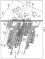
Fig. 3 is a cross-sectional perspective view of the connector shown inFig. 2 . -
Fig. 4 is a perspective view of an alternative configuration of the connector of the present invention. -
Fig. 5A is a cross-sectional view of an alternative embodiment of the contact of the present invention. -
Fig. 5B is a close-up, perspective view of the electrical interface of the embodiment ofFig. 5A . - Referring to
Figs. 1 - 3 , one embodiment of theconnector 200 of the present invention is shown. Theconnector 200 comprises ahousing 222 defining one ormore cavities 220. Disposed in one of thecavities 220 is acontact 100, having a front and rear orientation. Thecontact 100 comprises acontact housing 101. The contact housing is narrower than the cavity and resiliently disposed within therein such that the contact housing is laterally movable within the cavity to accommodate lateral offset of amating connector contact 221. Thecontact 100 comprises anoptical interface 102 for receiving aferrule 230 of themating connector contact 221. Thecontact 100 also comprisesoptoelectrical circuitry 104 optically connected to the optical interface, wherein the optical interface and the optoelectrical circuitry are held rigidly in relation to each other within the contact housing. The contact also comprises anelectrical interface 103 electrically connected to theoptoelectrical circuitry 104 and configured for electrical connection to acircuit board 224. Theelectrical interface 103 comprising at least aflexible cable 103a to provide compliance between the optoelectrical circuitry and the circuit board. These features are considered below in greater detail, and with respect to selected alternative embodiments. - The
housing 222 functions to define one or more cavities for holding one or more contacts in relation to thecircuit board 224. For example, in one embodiment, thehousing 222 defines fourdiscrete cavities 220 for holding four contacts. Such housings are known in the art, and, consequently, will not be described in detail herein. Suffice to say that in one embodiment, asocket portion 222a of thehousing 222 is secured to the circuit board via fasteners or other known means. Thesocket portion 222a contains the contacts. Aplug portion 222b, which houses the mating connector contacts, is configured to plug into thesocket portion 222a. Commonly, but not necessarily, the plug portion secures to the second portion using ascrew mechanism 231. - The
cavity 220 defined by the housing has a larger circumference than that of the contact housing to allow for radial movement of the contact within the cavity. More specifically, in one embodiment, when the contact is centered within the cavity, there is agap 232 around the contact which allows the contact freedom to move laterally. In one embodiment, to keep the contact biased in the center of the cavity, aspring member 223 is disposed in thecavity 220 and is configured to urge against the contact around its perimeter to center the contact within the cavity. Although aspring member 223 is shown in this embodiment, it should be understood that other embodiments are possible to resiliently position the contact in the center of the cavity. For example, rather than a spring member, elastic material may be disposed in the cavity between the contact and the wall the cavity. Still other alternative embodiments will be obvious to those of skill in the art in the light of this disclosure. - In this particular embodiment, the contact is configured to be held axially within the
housing 222. Specifically, the contact housing comprises aridge 233, and thespring member 223 is configured to bias theridge 233 rearward such that it contacts ashoulder 234 of thehousing 222, thereby holding thecontact housing 101 in a constant axial position with respect to thehousing 222, - The contact of the present invention is an active contact and functions to optically connect with a mating connector contact and convert between electrical and optical signals. The functionality of such active contact is known. For example, in one embodiment, the contact is a high speed active Quadrax contact. In one embodiment, the connector is configured with multiple cavities to accommodate multiple contacts. In one embodiment, all of the contacts are the same. In an alternative embodiment, at least two of the contacts are different types of contacts. For example, one contact may be an active contact and there other contact may be an electrical contact. Still other embodiments will be obvious to those of skill the art in the light of this disclosure.
- In one embodiment, the contact housing comprises a
discrete front portion 101a as shown inFig. 1 . Thefront portion 101a, in this embodiment, houses a ferrule receiving bore orsleeve 102c (discussed below). Such an embodiment facilitates manufacturing, although, other embodiments are possible within the scope of the invention. For example, in one embodiment, thefront portion 101a is integrated with themain contact housing 101. Those of skill in the art in the light of this disclosure will be able to optimize the contact housing for manufacturability and performance. - The
optical interface 102 functions to optically couple with a mating connector contact. In one embodiment, theoptical interface 102 of the present invention is a conventional optical interface. For example, as shown inFigs. 1-3 , the optical interface may be a conventional physical contact optical interface comprising aferrule 102a holding afiber 102b, and a ferrulereceiving bore orsleeve 102c for receiving themating ferrule 230. Alternatively, theoptical interface 102 may be an expanded beam optical interface in which the beam between the mating connector contact and the optical interface is expanded to enhance coupling performance. The expanded beam optical interface may involve physical contact and/or air gap(s). Expanded beam connectors are well-known and will not be described herein in detail. Still other optical interfaces will be obvious to those of skill in the art in the light of this disclosure. - The
optoelectrical circuitry 104a functions to convert between optical and electrical signals. Such circuitry is known. For example, in the embodiment ofFig. 1 ,optoelectrical circuitry 104 comprises aninterposer 104 to whichfiber 102b is optically coupled. Theinterposer 104a is mounted perpendicularly to acircuit board 104b. Such a configuration is known and disclosed for example inUS application No. 16/450,189 - An important feature of this embodiment of the present invention is that the
optical interface 102 is rigidly held relative to theoptoelectrical circuitry 104. As mentioned above, the applicant recognizes that such packaging provides for a more robust connector. In one embodiment, as shown inFig. 1 , the optical interface and the optoelectrical circuitry are affixed rigidly to the contact housing. Alternatively, theoptical interface 102 and theoptoelectrical circuitry 104 may be combined in a unitary subassembly which is disposed in thecontact 100. For example, in one embodiment, theoptoelectrical circuitry 104 may be potted with the tail end of the optical interface to form a robust hermetically sealed package. Still other embodiments will be obvious to those of skill in the art in the light of this disclosure. - The
electrical interface 103 functions not only to provide an electrical connection between theoptoelectrical circuitry 104 and thecircuit board 224, but also to provide compliance to allow thecontact 100 to move within thecavity 220 of thehousing 222. To this end, in one embodiment, theelectrical interface 103 comprises aflexible cable 103a. In one embodiment, the flexible cable comprises flexible printed circuit. - The configuration of this cable may vary. For example, in one embodiment, the
flexible cable 103a extends rearwardly from the contact and is electrically connected to the circuit board either by connectorized connections or by soldering. More specifically, the distal end of theflexible cable 103a may be terminated with aconnector 227, which is then coupled to a receiving connector on the circuit board. Such connectors are well-known and include, for example, a ZIF connector or other small connector. Alternatively, the distal end of thecable 103a may be bar soldered to the circuit board using known techniques. Still other means of electrically connecting the distal end of theflexible cable 103a to the circuit board will be known to those of skill in the art in the light of this disclosure. - Alternatively, rather than the distal end of the
flexible cable 103a being electrically connected to the circuit board, in another embodiment, theflexible cable 103a does not extend from thecontact 100, but rather connects theoptoelectrical circuitry 104 to an electrical connector disposed at the rear end of the contact. More specifically, referring toFig. 5A , one embodiment of an alternative embodiment of thecontact 500 having anelectrical interface 503 is shown. In this embodiment, theelectrical interface 503 comprises apin connector 503b which is electrically couple to theoptoelectrical circuitry 504 with theflexible cable 503a. In one embodiment, thepin connector 503b is configured to float within thecontact housing 501. More specifically, as shown inFig. 5b , which is a close-up view of theelectrical interface 503 of the embodiment ofFig. 5A , thepin connector 503b is centrally biased within thecontact housing 501 by resilient member(s) 504. Thus,pin connector 503b can move radially with respect to thecontact housing 501. It should be understood this is just one alternative embodiment of theelectrical interface 103 and that other alternative embodiments will be obvious to those of skill in the art in the light of this disclosure. - The
electrical interface 103 involves various embodiments of connection to thecircuit board 224. In one embodiment, shown inFigs. 1 - 3 , the circuit board has first and second sides, 224a, 224b, respectively, with theconnector housing 222 being mounted to thefirst side 224a, and theelectrical interface 104 electrically connected to the second side to 224b of thecircuit board 222. In one embodiment, theflexible cable 103a of each contact passes through adiscrete opening 225 defined in thecircuit board 224. To protect against chafing, in one embodiment, agrommet 228 is inserted in theopening 225. Alternatively, in one embodiment, rather than having discrete openings for each flexible cable extending from each contact, a common opening may be used as shown inFig. 4 . Specifically,Fig. 4 shows aconnector 400 having acircuit board 424 with asingle opening 425 through which all of the flexible cables of each contact pass. As with the individual discrete openings, in one embodiment, agrommet 428 is used to prevent chafing of the optical cables. Still other embodiments will be obvious to those of skill in the art in the light of this disclosure. - Referring back to
Figs. 3 and4 , in one embodiment, the flexible cable forms aservice bend 226 to accommodate movement of the contact relative to thehousing 222. More specifically, due to the necessary minimum bend radius of the cable, the right angle bend of the cable between the contact and its electrical connection to thecircuit board 224 results in a movement accommodating bend in the cable, which is referred herein as theservice bend 226. Thisservice bend 226 allows for movement of the contact relative to the circuit board with little resistance. As mentioned above, this relative movement is necessary to accommodate any misalignment between the mating connector contact and the contact of the present invention.
Claims (15)
- A connector (200) comprising:a housing (222, 222a, 222b) defining at least one cavity (220);a contact (100) within said at least one cavity (220), said contact (100) having a front and rear orientation, and comprising at least,a contact housing (101), said contact housing (101) being narrower than said at least one cavity (220) and resiliently disposed within said at least one cavity (220) such that said contact housing (101) is laterally movable within said cavity (220) to accommodate lateral offset of a mating connector contact (221);an optical interface (102) for receiving a ferrule (230) of said mating connector contact (221);optoelectrical circuitry (104) optically connected to said optical interface (102), wherein said optical interface (102) and said optoelectrical circuitry (104) are held rigidly in relation to each other within said contact housing (101); andan electrical interface (103) electrically connected to said optoelectrical circuitry (104) and configured for electrical connection to a circuit board (224), wherein said electrical interface (103) comprises at least a flexible cable (103a) to provide compliance between said optoelectrical circuitry (104) and said circuit board (224).
- The connector (200) of claim 1, wherein said optical interface (102) and said optoelectrical circuitry (104) are affixed rigidly to said contact housing (101).
- The connector (200) of claim 1 or 2, wherein said at least one contact (100) is not axially movable within said at least one cavity (220).
- The connector (200) of any preceding claim, wherein said flexible cable (103a) is connected to an electrical connector (227).
- The connector (200) of claim 4, wherein said electrical connector (503b) is resiliently disposed at a rear of said contact housing (501) such that said electrical connector (503b) is laterally moveable relative to said contact housing (501).
- The connector (200) of claim 5, wherein said electrical connector (503b) is a pin connector.
- The connector (200) of any preceding claim, further comprising a circuit board (224), and wherein said flexible cable (103a) is electrically connected to said circuit board (224).
- The connector (200) of claim 7, wherein said circuit board (224) defines and at least one opening (225) and a first (224a) and second side (224b), wherein said housing (222, 222a, 222b) is mounted on said first side (224a), wherein said flexible cable (103a) is electrically connected to said circuit board (224) on said second side (224b), and wherein said flexible cable (103a) passes through said at least one opening (225)
- The connector (200) of claim 8, further comprising a gromet (228) disposed around said opening (225).
- The connector (200) of any preceding claim, wherein said flexible cable (103a) bends about 90° forming a service bend (226) for accommodating movement of said contact (100).
- The connector 200 of claim 7 or any claim depending thereon, wherein said flexible cable (103a) is hot-bar soldered to said circuit board (224).
- The connector (200) of any preceding claim, wherein said flexible cable (103a) is terminated with a cable connector (227).
- The connector (200) of claim 12, wherein said cable connector (227) is a ZIF connector.
- The connector (400) of claim 8 or any claim depending thereon, wherein said at least one opening (425) is a common opening through which each flexible cable (103a) of each contact (100) passes.
- The connector (200) of claim 8 or any claim depending thereon, wherein said at least one opening (225) comprises a plurality of openings (225) wherein each flexible cable (103a) of each contact (100) passes through one of said plurality of openings (225).
Applications Claiming Priority (1)
| Application Number | Priority Date | Filing Date | Title |
|---|---|---|---|
| US17/540,692 US12013584B2 (en) | 2021-12-02 | 2021-12-02 | High-speed active contact |
Publications (1)
| Publication Number | Publication Date |
|---|---|
| EP4191308A1 true EP4191308A1 (en) | 2023-06-07 |
Family
ID=84367107
Family Applications (1)
| Application Number | Title | Priority Date | Filing Date |
|---|---|---|---|
| EP22210618.9A Pending EP4191308A1 (en) | 2021-12-02 | 2022-11-30 | High-speed active contact |
Country Status (3)
| Country | Link |
|---|---|
| US (1) | US12013584B2 (en) |
| EP (1) | EP4191308A1 (en) |
| JP (1) | JP2023082683A (en) |
Citations (5)
| Publication number | Priority date | Publication date | Assignee | Title |
|---|---|---|---|---|
| FR2691264A1 (en) * | 1992-05-12 | 1993-11-19 | Aerospatiale | Optical links joining system for coupling to electrical links - has opto-electronic component with fixed coupling able to convert optical signal to electrical signal with several electrical conductors |
| US20060008213A1 (en) * | 2004-07-12 | 2006-01-12 | Protokraft, Llc | Wall mount fiber optic connector and associated method for forming the same |
| US20200288572A1 (en) * | 2019-11-11 | 2020-09-10 | Dongguan Luxshare Technologies Co., Ltd | Circuit device |
| US10782494B2 (en) * | 2012-07-30 | 2020-09-22 | Glenair, Inc. | Advanced fiber-optic contact and method |
| US10872494B2 (en) | 2012-01-10 | 2020-12-22 | Universal Entertainment Corporation | System capable of adding multi-currency function |
Family Cites Families (24)
| Publication number | Priority date | Publication date | Assignee | Title |
|---|---|---|---|---|
| US3790791A (en) * | 1972-07-20 | 1974-02-05 | Bunker Ramo | Optoelectronic cable assembly |
| US4595839A (en) * | 1982-09-30 | 1986-06-17 | Tetra-Tech, Inc. | Bidirectional optical electronic converting connector with integral preamplification |
| US4666228A (en) * | 1983-09-28 | 1987-05-19 | Pave Technology Co. | Hermetic connector and method |
| US4798441A (en) * | 1987-03-09 | 1989-01-17 | Itt Corporation | Fiber optic device coupling |
| US5448676A (en) * | 1993-06-21 | 1995-09-05 | Mcdonnell Douglas Corporation | Electro-optical contact coupling |
| US6004044A (en) * | 1995-05-03 | 1999-12-21 | Itt Cannon, Inc. | Optoelectric connector |
| US6234683B1 (en) * | 1999-09-13 | 2001-05-22 | Stratos Lightwave, Inc. | Field repairable hermaphroditic connector |
| US7439449B1 (en) * | 2002-02-14 | 2008-10-21 | Finisar Corporation | Flexible circuit for establishing electrical connectivity with optical subassembly |
| US6913402B2 (en) * | 2003-08-07 | 2005-07-05 | Stratos International, Inc. | Bulkhead mountable optoelectronic device |
| FR2882444B1 (en) * | 2005-02-24 | 2008-04-04 | Radiall Sa | CONTACT ELEMENT FOR MULTICONTACT CONNECTOR AND SUCH CONNECTOR |
| US7104701B1 (en) * | 2005-02-28 | 2006-09-12 | Stratos International, Inc. | Expanded beam converter for MIL-PRF-83526/17 optical connector |
| JP2007042529A (en) * | 2005-08-05 | 2007-02-15 | Hitachi Ltd | Connection terminal, connection terminal assembly and connection terminal assembly method |
| US7766557B2 (en) * | 2007-03-06 | 2010-08-03 | Stratos International, Inc. | Expanded beam connector and expanded beam optoelectronic device |
| US7690849B2 (en) * | 2007-05-16 | 2010-04-06 | Protokraft, Llc | Fiber optic connector, active contact inserts therefor, and associated methods |
| US9081156B2 (en) * | 2009-10-05 | 2015-07-14 | Finisar Corporation | Simplified and shortened parallel cable |
| US8371877B2 (en) * | 2010-05-05 | 2013-02-12 | Sabritec, Inc. | Electrical connector with printed circuit board subassembly |
| US8827567B2 (en) * | 2011-08-10 | 2014-09-09 | Tyco Electronics Corporation | Field-installable expanded beam connector system |
| US8708575B2 (en) * | 2011-11-11 | 2014-04-29 | Sae Magnetics (H.K.) Ltd. | Active optical connector using audio port |
| US10302876B2 (en) * | 2012-02-16 | 2019-05-28 | Te Connectivity Corporation | Multi-channel optical insert |
| US9819107B2 (en) * | 2013-11-26 | 2017-11-14 | Glenair, Inc. | Advanced panel mount connector and method |
| US9470847B2 (en) * | 2014-06-04 | 2016-10-18 | Tyco Electronics Corporation | Polarization maintaining connectors |
| US9465171B2 (en) * | 2014-06-10 | 2016-10-11 | Tyco Electronics Corporation | Short optical terminus |
| CN107924028B (en) * | 2015-04-15 | 2020-10-27 | 莫戈公司 | Optical Rotary Electrical Connector |
| US10180553B2 (en) * | 2017-02-17 | 2019-01-15 | Corning Research & Development Corporation | Terminal assemblies, end cap assemblies, and fiber optic enclosures incorporating the same |
-
2021
- 2021-12-02 US US17/540,692 patent/US12013584B2/en active Active
-
2022
- 2022-11-29 JP JP2022189889A patent/JP2023082683A/en active Pending
- 2022-11-30 EP EP22210618.9A patent/EP4191308A1/en active Pending
Patent Citations (5)
| Publication number | Priority date | Publication date | Assignee | Title |
|---|---|---|---|---|
| FR2691264A1 (en) * | 1992-05-12 | 1993-11-19 | Aerospatiale | Optical links joining system for coupling to electrical links - has opto-electronic component with fixed coupling able to convert optical signal to electrical signal with several electrical conductors |
| US20060008213A1 (en) * | 2004-07-12 | 2006-01-12 | Protokraft, Llc | Wall mount fiber optic connector and associated method for forming the same |
| US10872494B2 (en) | 2012-01-10 | 2020-12-22 | Universal Entertainment Corporation | System capable of adding multi-currency function |
| US10782494B2 (en) * | 2012-07-30 | 2020-09-22 | Glenair, Inc. | Advanced fiber-optic contact and method |
| US20200288572A1 (en) * | 2019-11-11 | 2020-09-10 | Dongguan Luxshare Technologies Co., Ltd | Circuit device |
Also Published As
| Publication number | Publication date |
|---|---|
| JP2023082683A (en) | 2023-06-14 |
| US12013584B2 (en) | 2024-06-18 |
| US20230176305A1 (en) | 2023-06-08 |
Similar Documents
| Publication | Publication Date | Title |
|---|---|---|
| US10921537B2 (en) | Optical communication assemblies | |
| KR101928129B1 (en) | Wide temperature range optical fiber connector with thermal expansion compensation | |
| US10466427B2 (en) | Optical module with integrated lens | |
| US6485192B1 (en) | Optical device having an integral array interface | |
| US6588943B1 (en) | Electro-optic connector module | |
| US7561763B2 (en) | Connector system for optical wave guides | |
| US5577146A (en) | Optical connectors | |
| US7690849B2 (en) | Fiber optic connector, active contact inserts therefor, and associated methods | |
| US10185094B2 (en) | Optical plug having a removable and replaceable nosepiece and a complimentary receptacle | |
| US9383519B2 (en) | Optical communication module with fiber submount and latching optics assembly | |
| US8858095B2 (en) | Optical-electrical connector having a resilient member for urging ferrule against lens member | |
| US9904020B2 (en) | Connecting component | |
| US10852496B2 (en) | Optoelectronic module, and device for toolessly mounting/demounting an optical contact element | |
| US9690059B2 (en) | Optical module | |
| US5809191A (en) | Optical connector | |
| CN106461885A (en) | Substrate mounted optical receptacle | |
| US10677999B2 (en) | Duplex-modulo optical blindmate connector having a carrier plate and connector housing | |
| US12013584B2 (en) | High-speed active contact | |
| WO2017102517A1 (en) | Optical connector assembly | |
| KR20010085914A (en) | Connector system for fibre optic male contacts | |
| US8107823B2 (en) | Optical transmission module | |
| US20250306294A1 (en) | On-Package Self-Aligning Expanded-Beam Connector | |
| US20250093597A1 (en) | Opto-electrical connection system, and opto-electrical connector | |
| GB2525657A (en) | An optical connector assembly, an optical printed circuit board assembly, an insert and a method of manufacturing an optical connector assembly | |
| JP2000075172A (en) | Optical module |
Legal Events
| Date | Code | Title | Description |
|---|---|---|---|
| PUAI | Public reference made under article 153(3) epc to a published international application that has entered the european phase |
Free format text: ORIGINAL CODE: 0009012 |
|
| STAA | Information on the status of an ep patent application or granted ep patent |
Free format text: STATUS: THE APPLICATION HAS BEEN PUBLISHED |
|
| AK | Designated contracting states |
Kind code of ref document: A1 Designated state(s): AL AT BE BG CH CY CZ DE DK EE ES FI FR GB GR HR HU IE IS IT LI LT LU LV MC ME MK MT NL NO PL PT RO RS SE SI SK SM TR |
|
| STAA | Information on the status of an ep patent application or granted ep patent |
Free format text: STATUS: REQUEST FOR EXAMINATION WAS MADE |
|
| 17P | Request for examination filed |
Effective date: 20231207 |
|
| RBV | Designated contracting states (corrected) |
Designated state(s): AL AT BE BG CH CY CZ DE DK EE ES FI FR GB GR HR HU IE IS IT LI LT LU LV MC ME MK MT NL NO PL PT RO RS SE SI SK SM TR |
|
| STAA | Information on the status of an ep patent application or granted ep patent |
Free format text: STATUS: EXAMINATION IS IN PROGRESS |
|
| 17Q | First examination report despatched |
Effective date: 20241205 |