EP4187540A1 - Phase change memory device with improved retention characteristics and related method - Google Patents
Phase change memory device with improved retention characteristics and related method Download PDFInfo
- Publication number
- EP4187540A1 EP4187540A1 EP22209608.3A EP22209608A EP4187540A1 EP 4187540 A1 EP4187540 A1 EP 4187540A1 EP 22209608 A EP22209608 A EP 22209608A EP 4187540 A1 EP4187540 A1 EP 4187540A1
- Authority
- EP
- European Patent Office
- Prior art keywords
- memory
- percentage
- memory element
- phase change
- pulse
- Prior art date
- Legal status (The legal status is an assumption and is not a legal conclusion. Google has not performed a legal analysis and makes no representation as to the accuracy of the status listed.)
- Pending
Links
Images


Classifications
-
- G—PHYSICS
- G11—INFORMATION STORAGE
- G11C—STATIC STORES
- G11C11/00—Digital stores characterised by the use of particular electric or magnetic storage elements; Storage elements therefor
- G11C11/56—Digital stores characterised by the use of particular electric or magnetic storage elements; Storage elements therefor using storage elements with more than two stable states represented by steps, e.g. of voltage, current, phase, frequency
-
- G—PHYSICS
- G11—INFORMATION STORAGE
- G11C—STATIC STORES
- G11C13/00—Digital stores characterised by the use of storage elements not covered by groups G11C11/00, G11C23/00, or G11C25/00
- G11C13/0002—Digital stores characterised by the use of storage elements not covered by groups G11C11/00, G11C23/00, or G11C25/00 using resistive RAM [RRAM] elements
- G11C13/0004—Digital stores characterised by the use of storage elements not covered by groups G11C11/00, G11C23/00, or G11C25/00 using resistive RAM [RRAM] elements comprising amorphous/crystalline phase transition cells
-
- G—PHYSICS
- G11—INFORMATION STORAGE
- G11C—STATIC STORES
- G11C13/00—Digital stores characterised by the use of storage elements not covered by groups G11C11/00, G11C23/00, or G11C25/00
- G11C13/0002—Digital stores characterised by the use of storage elements not covered by groups G11C11/00, G11C23/00, or G11C25/00 using resistive RAM [RRAM] elements
- G11C13/0021—Auxiliary circuits
- G11C13/0069—Writing or programming circuits or methods
-
- H—ELECTRICITY
- H10—SEMICONDUCTOR DEVICES; ELECTRIC SOLID-STATE DEVICES NOT OTHERWISE PROVIDED FOR
- H10N—ELECTRIC SOLID-STATE DEVICES NOT OTHERWISE PROVIDED FOR
- H10N70/00—Solid-state devices having no potential barriers, and specially adapted for rectifying, amplifying, oscillating or switching
- H10N70/20—Multistable switching devices, e.g. memristors
- H10N70/231—Multistable switching devices, e.g. memristors based on solid-state phase change, e.g. between amorphous and crystalline phases, Ovshinsky effect
-
- H—ELECTRICITY
- H10—SEMICONDUCTOR DEVICES; ELECTRIC SOLID-STATE DEVICES NOT OTHERWISE PROVIDED FOR
- H10N—ELECTRIC SOLID-STATE DEVICES NOT OTHERWISE PROVIDED FOR
- H10N70/00—Solid-state devices having no potential barriers, and specially adapted for rectifying, amplifying, oscillating or switching
- H10N70/801—Constructional details of multistable switching devices
- H10N70/821—Device geometry
- H10N70/826—Device geometry adapted for essentially vertical current flow, e.g. sandwich or pillar type devices
-
- H—ELECTRICITY
- H10—SEMICONDUCTOR DEVICES; ELECTRIC SOLID-STATE DEVICES NOT OTHERWISE PROVIDED FOR
- H10N—ELECTRIC SOLID-STATE DEVICES NOT OTHERWISE PROVIDED FOR
- H10N70/00—Solid-state devices having no potential barriers, and specially adapted for rectifying, amplifying, oscillating or switching
- H10N70/801—Constructional details of multistable switching devices
- H10N70/841—Electrodes
- H10N70/8413—Electrodes adapted for resistive heating
-
- H—ELECTRICITY
- H10—SEMICONDUCTOR DEVICES; ELECTRIC SOLID-STATE DEVICES NOT OTHERWISE PROVIDED FOR
- H10N—ELECTRIC SOLID-STATE DEVICES NOT OTHERWISE PROVIDED FOR
- H10N70/00—Solid-state devices having no potential barriers, and specially adapted for rectifying, amplifying, oscillating or switching
- H10N70/801—Constructional details of multistable switching devices
- H10N70/881—Switching materials
- H10N70/882—Compounds of sulfur, selenium or tellurium, e.g. chalcogenides
- H10N70/8828—Tellurides, e.g. GeSbTe
-
- G—PHYSICS
- G11—INFORMATION STORAGE
- G11C—STATIC STORES
- G11C13/00—Digital stores characterised by the use of storage elements not covered by groups G11C11/00, G11C23/00, or G11C25/00
- G11C13/0002—Digital stores characterised by the use of storage elements not covered by groups G11C11/00, G11C23/00, or G11C25/00 using resistive RAM [RRAM] elements
- G11C13/0021—Auxiliary circuits
- G11C13/0069—Writing or programming circuits or methods
- G11C2013/0078—Write using current through the cell
Definitions
- the present invention relates to a phase change memory device with improved retention characteristics and a related method.
- non-volatile phase-change memories use materials that can switch between two or more stable phases characterized by different electrical properties. For instance, such materials are able to switch between a disorderly, amorphous, phase and an orderly, crystalline or polycrystalline phase, and the two phases are associated to resistivities having considerably different values that may be used to store data.
- the elements of Group VI of the Periodic Table such as tellurium (Te), selenium (Se), germanium (Ge) or antimony (Sb), referred to as chalcogenides or chalcogenic materials, are commonly used.
- Phase changes are obtained by locally increasing the temperature of the cells of chalcogenic material, through resistive electrodes (generally known as heaters) arranged in contact with respective regions of chalcogenic material.
- resistive electrodes generally known as heaters
- figure 1 shows a cross-section of a typical phase change memory element 1, with a wall-shaped heater.
- Phase change memory element 1 includes a memory region 2 of a chalcogenic material, in contact with a first electrode 3, here a bottom electrode, and with a second electrode 4, here an upper electrode.
- Memory region 2 may be a Ge x Sb y Te z alloy (also known as GST), for example Ge 2 Sb 2 Te 5 .
- Electrodes 3, 4 are of an electrically conductive material, for example TiN or TaN.
- the first electrode 3 has a lesser width than the second electrode 4.
- the first electrode 3 may have a width of a few nanometers and be formed in a pore or in an elongated trench in a dielectric layer 5 (the latter configuration, also called wall configuration). Due to its reduced width, current flowing in the first electrode 3 is concentrated and causes heating of a portion 9 of the memory region 2 above a contact area 8. Thus, first electrode 3 forms a heater.
- Portion 9 of the memory region 2 above contact area 8 when heated, undergoes phase change and forms an active portion 9.
- a selection device (for example, a MOSFET, not shown) is connected to the first electrode/heater 3 and enables passage of an electric program/reset current.
- the electric current by Joule effect, heats the chalcogenic material to obtain the desired temperature for phase-change.
- phase change memory element 1 to its crystalline state (low resistance state, also called set state)
- an electrical pulse is applied to heat the memory region 2 above its crystallization temperature.
- the phase change portion 9 maintains the polycrystalline phase. See, e.g., figure 2A .
- phase change memory element 1 To reset the phase change memory element 1 to the amorphous phase (high resistance state, also called reset state), the material is first heated to a higher temperature than during programming in order to melt it. By abruptly cutting off the electrical current pulse, the phase-change material quenches into its amorphous phase. See, e.g., figure 2B .
- Figure 3 shows exemplary plots of temperature T as a function of time t desired for programming operations associated to a reset pulse (continuous line) and a set pulse (dotted line) in the ideal condition of uniform temperature in the whole memory region 2.
- a decreasing temperature gradient is present, from the first electrode 3 to the second electrode 4.
- active portion 9 follows the shown behavior reported in figure 3 , and its temperature is equal or higher than those reported in figure 3 .
- the state of the chalcogenic material is detected by applying a voltage that is sufficiently low as avoid a considerable heating, and then by reading the current flowing in the memory element 1. Since the current is proportional to the conductivity of phase change memory element 1, it is possible to determine in which state the phase change memory element is and therefore to get the datum stored in the memory element.
- phase change memory elements are one of the most promising type of memory due to their easy integration with advanced logics and their costs, but their reliability is still not sufficient to meet the strict requirements existing in some applications, such as in the automotive field, where the thermal treatments provided therein may cause low data retention.
- an aim of the invention is to provide a phase-change memory device having a higher data retention capability.
- phase change memory element a phase change memory device and a method, as defined in the attached claims.
- FIG 4 shows a phase change memory element (hereafter, memory element 10) including a memory region 12 in contact with a first electrode (also called heater 13) and a second electrode 14 (also called upper electrode 14).
- first electrode also called heater 13
- second electrode 14 also called upper electrode 14
- memory region 12 is a Ge-rich GST alloy, that is an alloy that has general formula Ge x Sb y Te z but is not stoichiometric.
- the heater 13 has a small width (even a few nanometers) and is formed in a dielectric layer 15.
- the contact area between the heater 13 and the memory region 12 is indicated at 18.
- memory region 12 has a portion 12A above contact area 18; portion 12A (delimited in figure 4 by a dotted line) is configured to undergo phase change and thus forms an active zone 12A, surrounded by a bulk portion 12B of the memory region 12.
- Memory element 10 is generally coupled to a selection element to form a memory cell, as shown in figure 5 , wherein the memory cell is designated by 21 and selection element is designated by 22.
- FIG. 5 shows a phase change memory 20 comprising a memory array 25 including a plurality of memory cells 21.
- memory element 10 and selection element 12, here illustrated as a switch are series-coupled.
- Selection element 12 may be implemented through any suitable component, such as a diode, a bipolar transistor, a MOSFET transistor, as known in the art.
- Memory cells 21 are generally organised in rows and columns and are coupled, through a plurality of wordlines 23 and a plurality of bitlines 24, to a row decoder 26 and to a column decoder 27.
- Decoders 26, 27 enable selection of the memory cells 21, on the basis of address logic signals and more or less complex decoding schemes; in particular, they select the memory cell(s) 21 coupled to one or more wordlines 23 and one or more bitlines 24 that are addressed by the decoders 26, 27.
- Column decoder 26 and row decoder 27 are coupled to a control unit 28 and to a read/program unit 29.
- Read/program unit 29 may include a program circuit 29A and a read/verify circuit 29B.
- the program circuit 29A is configured to provide programming pulses (set or reset pulses) to selected memory cells 21. To this end, it comprises a current generator circuit 30.
- the read/verify circuit 29B is connected to the selected memory cells 21 for reading the information stored therein (e.g., to implement a verify operation after each programming pulse). Reading may be carried out by comparing the currents from one or more suitably biased memory cells 21 with read current reference levels (during a reading operation) or with program current reference levels (during a verify operation).
- this disclosure regards a memory element 10 having a memory region 12 of a Ge-rich GST alloy.
- Ge-rich GST indicates a GST alloy wherein germanium (Ge) is a predominant component of the average composition.
- the percentage of Ge in the GST alloy may be higher than 50%.
- Bulk zone 12B has the average percentage.
- a first alloy characterized by composition including 70% Ge, 10% Sb and 20% Te (referred to as GST 712) may be used.
- a second alloy characterized by composition including 65%Ge, 20%Sb and 15% Te (referred to as GST 621) may be used.
- Ge-rich GST alloys may be used.
- the GST alloy may include nitrogen and/or other residual ions that do not alter the basic working principles and the physical features of the GST alloy in terms of ions chemical and morphological distribution.
- Ge-rich GST alloys By studying the properties of Ge-rich GST alloys, the inventors have discovered that Ge-rich GST alloys, if programmed in the polycrystalline state by a programming pulse having a slow quenching pulse, have locally different compositions (portions with different stoichiometries). Thus, logic levels of Ge-rich memory element 10 may be associated to polycrystalline structures having, in the active zone, a plurality of locally different compositions (locally different polycrystalline structures).
- the active zone 12A of memory element 10 comprises a first portion that has a first stoichiometry, and a second portion that has a second stoichiometry, different from the first stoichiometry.
- the first portion (hereinafter called core portion 31, see also figure 7 ) is characterized by a local high concentration of Sb; the second portion (hereinafter called shell portion 32) is characterized by a local high concentration of Te.
- the percentage of Sb in the core portion 31 is higher than the percentage of Sb in the bulk portion 12B and the percentage of Te in the shell portion 32 is higher than the percentage of Te in the bulk portion 12B.
- the percentage of Sb in the core portion 31 is at least twice the percentage of Sb in the bulk portion 12B; in particular, in the case of the first alloy, the percentage of Sb in the core portion 31 may be at least four times.
- the percentage of Te in the shell portion 32 is at least twice than the percentage of Te in the bulk portion 12B.
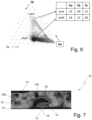
- figure 6 shows the compositional phase diagram of relative amounts of Te, Sb, and Ge in the memory region 12 of memory element 10 of figure 4 programmed in the set state and figure 7 shows a STEM-EELS image of the obtained chemical map.
- figure 6 shows that the core portion 31 has an Sb rich composition, with the percentage of Sb very high, higher than the percentages of Ge and Te, while shell portion 32 has a Te rich composition, wherein the percentage of Te is much higher than in the bulk zone 12B and, for the first alloy, comparable to the Ge percentage, considering the error of the technique and a 4-5% variability of the measurement.
- Figure 7 shows clearly the presence, in the memory region 12, of core portion 31, near the heater 13, and shell portion 32.
- core portion 31 and shell portion 32 form the active zone 12A of figure 4 .
- core portion 31 extends, dome-shaped, above the heater 13, and shell portion 32 extends deeper in the memory region 12, towards the upper electrode 14, surrounding almost completely core portion 31.
- Both the core portion 31 and the shell portion 32 have a polycrystalline structure.
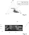
- Figure 8 and 9 show the compositional phase diagram of relative amounts of Te, Sb, and Ge in the memory region 12 of the same memory element 10 of figure 4 programmed in the reset state and a STEM-EELS image of the obtained chemical map.
- active zone 12A here forms an amorphous portion 33 having a uniform composition, wherein neither an Sb rich portion nor a Te rich portion is any more visible.
- amorphous portion 33 has a composition that is substantially uniform in the active zone 12A, with a well-defined distribution, clearly separated from the distribution in the bulk zone 12B, with limited dispersion.
- memory device 20 of figure 5 is able to generate programming pulses able to cause switching of the memory element 10 between the polycrystalline, differential stoichiometry state shown in figures 6 and 7 (set state, associated to a first logic value, for example with a logic 0) and the amorphous, uniform distribution state shown in figures 8 and 9 (reset state, associated to a second logic value, for example with a logic 1) .
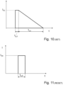
- the set/reset states of memory elements 10 may be obtained by applying a slow quenching pulse to get the polycrystalline, set state, and a fast quenching pulse to get the amorphous, reset state with uniform composition, as shown in figures 10 and 11 .
- Table 1 below indicates possible programming pulses, wherein I P,S is the plateau current during the set operation, I P,R is the plateau current during the reset operation, t r,S is the rise time of the pulse during the set operation, t r,R is the rise time of the pulse during the reset operation, t p,S is the plateau time of the pulse during the set operation, t p,R is the plateau time of the pulse during the reset operation, t f,S is the fall time of the pulse during the set operation, t f,R is the fall time of the pulse during the reset operation, sl S is the falling slope of the pulse during the set operation, and sl R is the falling slope of the pulse during the reset operation.
- the plateau current I P,S during the set operation is generally lower than the plateau current I P,R during the reset operation.
- the fall time tf,s during the set operation is much longer than the fall time t f,R during the reset operation.
- the fall time tf,s during the set operation may be at least ten times, for example almost 100 times the fall time t f,R during the reset operation.
- the current generator circuits 30, under control of the control unit 28 and the program circuit 29A, may generate the slow quenching pulses to get the polycrystalline, set state ( figure 10 ) and the fast quenching pulses to get the amorphous, reset state with uniform composition ( figure 11 ).
- a positive voltage is applied to the second electrode 14, thereby drawing Sb ions (that are positively charged) toward the contact area 18, thereby causing formation of the core portion 31.
- Te ions that are negatively charged, remain mainly on top of the core portion 31, forming the shell portion 32.
- the uniform, Ge-rich distribution in the memory region 12 reached in the reset state allows the memory element 10 to be very stable and have a high retention time.
- the memory element 10 including a memory region 12 having a strong, non-stoichiometric, Ge-rich alloy discussed above, programmable to switch between the above discussed set and reset states, has thus improved performances as regards retention and reliability, that may satisfy the high automotive requirements.
- the memory element 10 is soldering resistant, so that any data written in the memory device 10 before soldering are not lost.
- the memory element 10 has high scalability, since the programming currents scale with cell area reduction.
- the memory element 10 is versatile, since the unipolar programming is suitable for both MOS and BJT selector technology.
- memory element 10 with a Ge-rich memory region 12 appropriately programmed in the set state, has the discussed locally different compositions discussed above, independently on the technology used.
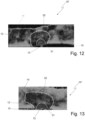
- figures 12 and 13 show two different memory elements 10', 10" programmed in the set state, having the general structure described with reference to figure 4 but with heaters 13 formed by different technologies and materials.
- memory elements 10', 10" have a differential structure, with a core portion 31 which is Sb-rich and a shell portion 32 which is Te-rich.
- the shell portions 32 completely surround the respective core portions 31, except, of course, the face thereof in contact with the heater 13 and the dielectric layer 15.
- any shape of the electrode suitable to heat the memory region to cause switching between the set and the reset state may be used.
Landscapes
- Chemical & Material Sciences (AREA)
- Crystallography & Structural Chemistry (AREA)
- Engineering & Computer Science (AREA)
- Computer Hardware Design (AREA)
- Semiconductor Memories (AREA)
Abstract
Description
- The present invention relates to a phase change memory device with improved retention characteristics and a related method.
- As is known, non-volatile phase-change memories (PCMs) use materials that can switch between two or more stable phases characterized by different electrical properties. For instance, such materials are able to switch between a disorderly, amorphous, phase and an orderly, crystalline or polycrystalline phase, and the two phases are associated to resistivities having considerably different values that may be used to store data.
- To this end, the elements of Group VI of the Periodic Table, such as tellurium (Te), selenium (Se), germanium (Ge) or antimony (Sb), referred to as chalcogenides or chalcogenic materials, are commonly used.
- Phase changes are obtained by locally increasing the temperature of the cells of chalcogenic material, through resistive electrodes (generally known as heaters) arranged in contact with respective regions of chalcogenic material. For example,
figure 1 shows a cross-section of a typical phasechange memory element 1, with a wall-shaped heater. - Phase
change memory element 1 includes amemory region 2 of a chalcogenic material, in contact with afirst electrode 3, here a bottom electrode, and with asecond electrode 4, here an upper electrode. -
Memory region 2 may be a GexSbyTez alloy (also known as GST), for example Ge2Sb2Te5. -
Electrodes first electrode 3 has a lesser width than thesecond electrode 4. For example, thefirst electrode 3 may have a width of a few nanometers and be formed in a pore or in an elongated trench in a dielectric layer 5 (the latter configuration, also called wall configuration). Due to its reduced width, current flowing in thefirst electrode 3 is concentrated and causes heating of aportion 9 of thememory region 2 above acontact area 8. Thus,first electrode 3 forms a heater. -
Portion 9 of thememory region 2 above contact area 8 (delimited infigure 1 by a dotted line), when heated, undergoes phase change and forms anactive portion 9. - A selection device (for example, a MOSFET, not shown) is connected to the first electrode/
heater 3 and enables passage of an electric program/reset current. The electric current, by Joule effect, heats the chalcogenic material to obtain the desired temperature for phase-change. - In particular, to program the phase
change memory element 1 to its crystalline state (low resistance state, also called set state), an electrical pulse is applied to heat thememory region 2 above its crystallization temperature. By allowing thememory region 2 to slowly cool down to normal operating temperature, thephase change portion 9 maintains the polycrystalline phase. See, e.g.,figure 2A . - To reset the phase
change memory element 1 to the amorphous phase (high resistance state, also called reset state), the material is first heated to a higher temperature than during programming in order to melt it. By abruptly cutting off the electrical current pulse, the phase-change material quenches into its amorphous phase. See, e.g.,figure 2B . -
Figure 3 shows exemplary plots of temperature T as a function of time t desired for programming operations associated to a reset pulse (continuous line) and a set pulse (dotted line) in the ideal condition of uniform temperature in thewhole memory region 2. In fact, a decreasing temperature gradient is present, from thefirst electrode 3 to thesecond electrode 4. In any case,active portion 9 follows the shown behavior reported infigure 3 , and its temperature is equal or higher than those reported infigure 3 . - During reading, the state of the chalcogenic material is detected by applying a voltage that is sufficiently low as avoid a considerable heating, and then by reading the current flowing in the
memory element 1. Since the current is proportional to the conductivity of phasechange memory element 1, it is possible to determine in which state the phase change memory element is and therefore to get the datum stored in the memory element. - Memories including phase change memory elements are one of the most promising type of memory due to their easy integration with advanced logics and their costs, but their reliability is still not sufficient to meet the strict requirements existing in some applications, such as in the automotive field, where the thermal treatments provided therein may cause low data retention.
- Thus, an aim of the invention is to provide a phase-change memory device having a higher data retention capability.
- According to the present invention, there are provided a phase change memory element, a phase change memory device and a method, as defined in the attached claims.
- For the understanding of the present invention, embodiments thereof are now described, purely as a non-limitative example, with reference to the enclosed drawings, wherein:
-
Figure 1 is a cross-section of a phase change memory element; -
Figures 2A and 2B are images obtained through dark-field (DF) scanning transmission electron microscope (STEM) of the phase change memory element offigure 1 in the set state and, respectively, in the reset state; -
Figure 3 shows exemplary plots of temperatures vs. time during set/reset operations of the phase change memory cell offigure 1 ; -
Figure 4 is a cross-section of a phase change memory element, according to an embodiment; -
Figure 5 is a schematic block diagram of a non-volatile memory including phase change memory elements; -
Figure 6 is a compositional phase diagram of relative amounts of ions in the memory phase change memory element offigure 4 programmed in the set state, according to an embodiment, -
Figure 7 shows an image obtained through Electron Energy Loss Spectroscopy performed by scanning transmission electron microscope (STEM-EELS) of the phase change memory element offigure 4 programmed in the set state; -
Figure 8 is a compositional phase diagram of relative amounts of ions in the phase change memory element offigure 4 programmed in the reset state, according to an embodiment, -
Figure 9 shows an image obtained through Electron Energy Loss Spectroscopy performed by_scanning transmission electron microscope (STEM-EELS) of the phase change memory element offigure 4 programmed in the reset state; -
Figures 10 and 11 show current pulses to program the phase change memory element in the set and, respectively, in the reset state, according to an embodiment; and -
Figures 12 and 13 are images obtained through Electron Energy Loss Spectroscopy performed by scanning transmission electron microscope (STEM-EELS) of different phase change memory elements programmed in the set state. -
Figure 4 shows a phase change memory element (hereafter, memory element 10) including amemory region 12 in contact with a first electrode (also called heater 13) and a second electrode 14 (also called upper electrode 14). - As discussed in detail hereinbelow,
memory region 12 is a Ge-rich GST alloy, that is an alloy that has general formula GexSbyTez but is not stoichiometric. - The
heater 13 has a small width (even a few nanometers) and is formed in adielectric layer 15. The contact area between theheater 13 and thememory region 12 is indicated at 18. - As shown in
figure 4 ,memory region 12 has aportion 12A abovecontact area 18;portion 12A (delimited infigure 4 by a dotted line) is configured to undergo phase change and thus forms anactive zone 12A, surrounded by abulk portion 12B of thememory region 12. -
Memory element 10 is generally coupled to a selection element to form a memory cell, as shown infigure 5 , wherein the memory cell is designated by 21 and selection element is designated by 22. -
Figure 5 shows aphase change memory 20 comprising amemory array 25 including a plurality ofmemory cells 21. In eachmemory cell 21,memory element 10 andselection element 12, here illustrated as a switch, are series-coupled.Selection element 12 may be implemented through any suitable component, such as a diode, a bipolar transistor, a MOSFET transistor, as known in the art. -
Memory cells 21 are generally organised in rows and columns and are coupled, through a plurality ofwordlines 23 and a plurality ofbitlines 24, to arow decoder 26 and to acolumn decoder 27.Decoders memory cells 21, on the basis of address logic signals and more or less complex decoding schemes; in particular, they select the memory cell(s) 21 coupled to one ormore wordlines 23 and one ormore bitlines 24 that are addressed by thedecoders -
Column decoder 26 androw decoder 27 are coupled to acontrol unit 28 and to a read/program unit 29. Read/program unit 29 may include aprogram circuit 29A and a read/verify circuit 29B. - The
program circuit 29A is configured to provide programming pulses (set or reset pulses) to selectedmemory cells 21. To this end, it comprises acurrent generator circuit 30. The read/verify circuit 29B is connected to theselected memory cells 21 for reading the information stored therein (e.g., to implement a verify operation after each programming pulse). Reading may be carried out by comparing the currents from one or more suitablybiased memory cells 21 with read current reference levels (during a reading operation) or with program current reference levels (during a verify operation). - As indicated above, this disclosure regards a
memory element 10 having amemory region 12 of a Ge-rich GST alloy. - Herein, the term "Ge-rich GST" indicates a GST alloy wherein germanium (Ge) is a predominant component of the average composition. In particular, the percentage of Ge in the GST alloy may be higher than 50%.
Bulk zone 12B has the average percentage. - In an embodiment, a first alloy, characterized by composition including 70% Ge, 10% Sb and 20% Te (referred to as GST 712) may be used.
- In another embodiment, a second alloy, characterized by composition including 65%Ge, 20%Sb and 15% Te (referred to as GST 621) may be used.
- However, other Ge-rich GST alloys may be used.
- In a per se known manner, the GST alloy may include nitrogen and/or other residual ions that do not alter the basic working principles and the physical features of the GST alloy in terms of ions chemical and morphological distribution.
- By studying the properties of Ge-rich GST alloys, the inventors have discovered that Ge-rich GST alloys, if programmed in the polycrystalline state by a programming pulse having a slow quenching pulse, have locally different compositions (portions with different stoichiometries). Thus, logic levels of Ge-
rich memory element 10 may be associated to polycrystalline structures having, in the active zone, a plurality of locally different compositions (locally different polycrystalline structures). - Thus, according to an embodiment, in the set state, the
active zone 12A ofmemory element 10 comprises a first portion that has a first stoichiometry, and a second portion that has a second stoichiometry, different from the first stoichiometry. - The first portion (hereinafter called
core portion 31, see alsofigure 7 ) is characterized by a local high concentration of Sb; the second portion (hereinafter called shell portion 32) is characterized by a local high concentration of Te. - In particular, the percentage of Sb in the
core portion 31 is higher than the percentage of Sb in thebulk portion 12B and the percentage of Te in theshell portion 32 is higher than the percentage of Te in thebulk portion 12B. - In addition, the percentage of Sb in the
core portion 31 is at least twice the percentage of Sb in thebulk portion 12B; in particular, in the case of the first alloy, the percentage of Sb in thecore portion 31 may be at least four times. - Furthermore, the percentage of Te in the
shell portion 32 is at least twice than the percentage of Te in thebulk portion 12B. - This is shown in
figures 6 and 7 for amemory element 10 whosememory region 12 is made of the above indicated first alloy. - Specifically,
figure 6 shows the compositional phase diagram of relative amounts of Te, Sb, and Ge in thememory region 12 ofmemory element 10 offigure 4 programmed in the set state andfigure 7 shows a STEM-EELS image of the obtained chemical map. - In particular,
figure 6 shows that thecore portion 31 has an Sb rich composition, with the percentage of Sb very high, higher than the percentages of Ge and Te, whileshell portion 32 has a Te rich composition, wherein the percentage of Te is much higher than in thebulk zone 12B and, for the first alloy, comparable to the Ge percentage, considering the error of the technique and a 4-5% variability of the measurement. -
Figure 7 shows clearly the presence, in thememory region 12, ofcore portion 31, near theheater 13, andshell portion 32. Thus,core portion 31 andshell portion 32 form theactive zone 12A offigure 4 . - As visible also in
figure 7 ,core portion 31 extends, dome-shaped, above theheater 13, andshell portion 32 extends deeper in thememory region 12, towards theupper electrode 14, surrounding almost completelycore portion 31. - Both the
core portion 31 and theshell portion 32 have a polycrystalline structure. -
Figure 8 and 9 show the compositional phase diagram of relative amounts of Te, Sb, and Ge in thememory region 12 of thesame memory element 10 offigure 4 programmed in the reset state and a STEM-EELS image of the obtained chemical map. - As visible in
figure 9 ,active zone 12A here forms anamorphous portion 33 having a uniform composition, wherein neither an Sb rich portion nor a Te rich portion is any more visible. - In particular, as visible in the compositional phase diagram of
figure 8 ,amorphous portion 33 has a composition that is substantially uniform in theactive zone 12A, with a well-defined distribution, clearly separated from the distribution in thebulk zone 12B, with limited dispersion. - According to an embodiment, in use,
memory device 20 offigure 5 is able to generate programming pulses able to cause switching of thememory element 10 between the polycrystalline, differential stoichiometry state shown infigures 6 and 7 (set state, associated to a first logic value, for example with a logic 0) and the amorphous, uniform distribution state shown infigures 8 and 9 (reset state, associated to a second logic value, for example with a logic 1) . - The set/reset states of
memory elements 10 may be obtained by applying a slow quenching pulse to get the polycrystalline, set state, and a fast quenching pulse to get the amorphous, reset state with uniform composition, as shown infigures 10 and 11 . - For example, Table 1 below indicates possible programming pulses, wherein IP,S is the plateau current during the set operation, IP,R is the plateau current during the reset operation, tr,S is the rise time of the pulse during the set operation, tr,R is the rise time of the pulse during the reset operation, tp,S is the plateau time of the pulse during the set operation, tp,R is the plateau time of the pulse during the reset operation, tf,S is the fall time of the pulse during the set operation, tf,R is the fall time of the pulse during the reset operation, slS is the falling slope of the pulse during the set operation, and slR is the falling slope of the pulse during the reset operation.
Table 1 SET RESET IP,S / IP,R 50-300 µA 100-400 µA tp,S / tp,R 100-200 ns 50-300 ns tr,S / tr,R ≤ 30 ns ≤ 30 ns tf,S / tf,R 2-6 µs ≤ 30 ns slS / slR 45-150 µA/µs ≤ 10 µA/ns - In particular, the plateau current IP,S during the set operation is generally lower than the plateau current IP,R during the reset operation.
- In addition, the fall time tf,s during the set operation is much longer than the fall time tf,R during the reset operation. Specifically, the fall time tf,s during the set operation may be at least ten times, for example almost 100 times the fall time tf,R during the reset operation.
- With reference again to
figure 5 , thecurrent generator circuits 30, under control of thecontrol unit 28 and theprogram circuit 29A, may generate the slow quenching pulses to get the polycrystalline, set state (figure 10 ) and the fast quenching pulses to get the amorphous, reset state with uniform composition (figure 11 ). - In particular, in the set operation, a positive voltage is applied to the
second electrode 14, thereby drawing Sb ions (that are positively charged) toward thecontact area 18, thereby causing formation of thecore portion 31. Te ions, that are negatively charged, remain mainly on top of thecore portion 31, forming theshell portion 32. - Tests made by the Applicant have shown that the presence, in the set state, of highly conductive Sb in the
core portion 31 allows thememory element 10 to show enhanced conduction. - On the other hand, the uniform, Ge-rich distribution in the
memory region 12 reached in the reset state allows thememory element 10 to be very stable and have a high retention time. - The
memory element 10 including amemory region 12 having a strong, non-stoichiometric, Ge-rich alloy discussed above, programmable to switch between the above discussed set and reset states, has thus improved performances as regards retention and reliability, that may satisfy the high automotive requirements. - Therefore, the
memory element 10 is soldering resistant, so that any data written in thememory device 10 before soldering are not lost. - In addition, the
memory element 10 has high scalability, since the programming currents scale with cell area reduction. - Moreover, the
memory element 10 is versatile, since the unipolar programming is suitable for both MOS and BJT selector technology. - Test made by the Applicant has also shown that
memory element 10 with a Ge-rich memory region 12, appropriately programmed in the set state, has the discussed locally different compositions discussed above, independently on the technology used. - For example,
figures 12 and 13 show twodifferent memory elements 10', 10" programmed in the set state, having the general structure described with reference tofigure 4 but withheaters 13 formed by different technologies and materials. - As may be seen in
figures 12 and 13 , alsomemory elements 10', 10" have a differential structure, with acore portion 31 which is Sb-rich and ashell portion 32 which is Te-rich. - Here, in both
memory elements 10', 10", theshell portions 32 completely surround therespective core portions 31, except, of course, the face thereof in contact with theheater 13 and thedielectric layer 15. - Finally, it is clear that numerous variations and modifications may be made to the memory element, device and method described and illustrated herein, all falling within the scope of the invention as defined in the attached claims.
- For example, even if the above description refers to the heater formed in the wall configuration, any shape of the electrode suitable to heat the memory region to cause switching between the set and the reset state may be used.
Claims (12)
- A phase change memory element (10, 10'; 10") comprising a memory region (12), a first electrode (13), a second electrode (14), the memory region (12) arranged between the first and the second electrodes (13, 14) and having a bulk zone (12B) and an active zone (12A), the memory region (12) being a germanium, antimony and tellurium based alloy, with an average percentage of germanium in the memory region (12) higher than 50%,
wherein:the active zone (12A) is configured to switch between a first stable state associated to a first memory logic level and a second stable state associated to a second memory logic level,the active zone (12A) has, in the first stable state, a uniform, amorphous structure and, in the second stable state, a differential polycrystalline structure including a first portion (31), having a first stoichiometry, and a second portion (32), having a second stoichiometry, different from the first stoichiometry. - A phase change memory element according to the preceding claim, wherein, in the second stable state, the first portion (31) has a first percentage of antimony and a first percentage of tellurium, and the second portion (32) has a second percentage of antimony, lower than the first percentage of antimony, and a second percentage of tellurium, higher than the first percentage of tellurium.
- A phase change memory element according to the preceding claim, wherein the first percentage of antimony is higher than a percentage of antimony in the bulk portion (12B) and the second percentage of tellurium is higher than a percentage of tellurium in the bulk portion.
- A phase change memory element according to claim 2 or 3, wherein the first percentage of antimony is at least twice the percentage of antimony in the bulk portion (12B).
- A phase change memory element according to any of the preceding claims, wherein the second percentage of tellurium is at least twice the percentage of tellurium in the bulk portion (12B) .
- A phase change memory element according to any of the preceding claims, wherein the first portion (31) is adjacent the first electrode (13).
- A phase change memory element according to any of the preceding claims, wherein the second portion (32) is adjacent the first portion (31).
- A memory device according to any of the preceding claims, wherein the first portion (31) is dome-shaped and the second portion (32) is shell-shaped and at least partially surrounds the first portion (31).
- A memory device (20) comprising a plurality of memory cells (21), each memory cell (21) including a memory element (10; 10'; 10") according any of the preceding claims, the memory device (20) comprising circuit elements (30) configured to bias the memory elements (10; 10'; 10") of the memory cells (21) and to cause the memory elements (10; 10'; 10") of addressed memory cells (21) to switch between the first and the second stable state.
- A method for programming a memory element (10; 10'; 10") according to any of claims 1 to 8, comprising:selectively supplying the memory element with a bias pulse selected from a first bias pulse and a second bias pulse,the first bias pulse causing the memory element to switch in the first stable state;the second bias pulse causing the memory element to switch in the second stable state;wherein the first and second bias pulses have a respective height and a respective fall time, the height of the first pulse being greater than the height of the second pulse and the fall time of the first pulse being shorter than the fall time of the second pulse.
- A method according to the preceding claim, wherein the fall time (tf,S) of the second bias pulse is at least ten times the fall time (tf,R) of the first pulse.
- A method according to claim 10 to 11, wherein the fall time (tf,S) of the second bias pulse is almost 100 times the fall time (tf,R) of the second bias pulse.
Applications Claiming Priority (1)
| Application Number | Priority Date | Filing Date | Title |
|---|---|---|---|
| IT202100030293 | 2021-11-30 |
Publications (1)
| Publication Number | Publication Date |
|---|---|
| EP4187540A1 true EP4187540A1 (en) | 2023-05-31 |
Family
ID=80225450
Family Applications (1)
| Application Number | Title | Priority Date | Filing Date |
|---|---|---|---|
| EP22209608.3A Pending EP4187540A1 (en) | 2021-11-30 | 2022-11-25 | Phase change memory device with improved retention characteristics and related method |
Country Status (3)
| Country | Link |
|---|---|
| US (1) | US12266402B2 (en) |
| EP (1) | EP4187540A1 (en) |
| CN (1) | CN116206652A (en) |
Cited By (1)
| Publication number | Priority date | Publication date | Assignee | Title |
|---|---|---|---|---|
| IT202300009990A1 (en) * | 2023-05-17 | 2024-11-17 | St Microelectronics Int Nv | PHASE CHANGE MEMORY ELEMENT PARTICULARLY SUITABLE FOR EMBEDDED AND AUTOMOTIVE APPLICATIONS |
Citations (1)
| Publication number | Priority date | Publication date | Assignee | Title |
|---|---|---|---|---|
| US20150371704A1 (en) * | 2014-06-18 | 2015-12-24 | Macronix International Co., Ltd. | Method and apparatus for healing phase change memory devices |
Family Cites Families (9)
| Publication number | Priority date | Publication date | Assignee | Title |
|---|---|---|---|---|
| US8809829B2 (en) * | 2009-06-15 | 2014-08-19 | Macronix International Co., Ltd. | Phase change memory having stabilized microstructure and manufacturing method |
| US8634235B2 (en) | 2010-06-25 | 2014-01-21 | Macronix International Co., Ltd. | Phase change memory coding |
| US8946666B2 (en) * | 2011-06-23 | 2015-02-03 | Macronix International Co., Ltd. | Ge-Rich GST-212 phase change memory materials |
| US10318861B2 (en) * | 2015-06-17 | 2019-06-11 | International Business Machines Corporation | Artificial neuron apparatus |
| US10217046B2 (en) * | 2015-06-29 | 2019-02-26 | International Business Machines Corporation | Neuromorphic processing devices |
| US10268949B2 (en) * | 2016-03-21 | 2019-04-23 | International Business Machines Corporation | Artificial neuron apparatus |
| US10423878B2 (en) * | 2016-09-07 | 2019-09-24 | International Business Machines Corporation | Artificial neuron apparatus |
| CN111279501B (en) * | 2020-01-16 | 2021-05-14 | 长江存储科技有限责任公司 | Phase change memory |
| US11978511B2 (en) * | 2021-07-23 | 2024-05-07 | Taiwan Semiconductor Manufacturing Company, Ltd. | Phase-change memory cell and method for fabricating the same |
-
2022
- 2022-11-23 US US17/993,118 patent/US12266402B2/en active Active
- 2022-11-25 EP EP22209608.3A patent/EP4187540A1/en active Pending
- 2022-11-29 CN CN202211513757.1A patent/CN116206652A/en active Pending
Patent Citations (1)
| Publication number | Priority date | Publication date | Assignee | Title |
|---|---|---|---|---|
| US20150371704A1 (en) * | 2014-06-18 | 2015-12-24 | Macronix International Co., Ltd. | Method and apparatus for healing phase change memory devices |
Non-Patent Citations (3)
| Title |
|---|
| PADILLA ALVARO ET AL: "Voltage polarity effects in GeSbTe-based phase change memory devices", JOURNAL OF APPLIED PHYSICS, AMERICAN INSTITUTE OF PHYSICS, 2 HUNTINGTON QUADRANGLE, MELVILLE, NY 11747, vol. 110, no. 5, 1 September 2011 (2011-09-01), pages 1 - 12, XP012154317, ISSN: 0021-8979, [retrieved on 20110901], DOI: 10.1063/1.3626047 * |
| REDAELLI ANDREA ET AL: "Material and process engineering challenges in Ge-rich GST for embedded PCM", vol. 137, 29 September 2021 (2021-09-29), UK, pages 1 - 8, XP055930156, ISSN: 1369-8001, Retrieved from the Internet <URL:http://dx.doi.org/10.1016/j.mssp.2021.106184> [retrieved on 20220613], DOI: 10.1016/j.mssp.2021.106184 * |
| ZHANG WEI ET AL: "Unveiling the structural origin to control resistance drift in phase-change memory materials", MATERIALS TODAY, ELSEVIER, AMSTERDAM, NL, vol. 41, 13 August 2020 (2020-08-13), pages 156 - 176, XP086396623, ISSN: 1369-7021, [retrieved on 20200813], DOI: 10.1016/J.MATTOD.2020.07.016 * |
Cited By (2)
| Publication number | Priority date | Publication date | Assignee | Title |
|---|---|---|---|---|
| IT202300009990A1 (en) * | 2023-05-17 | 2024-11-17 | St Microelectronics Int Nv | PHASE CHANGE MEMORY ELEMENT PARTICULARLY SUITABLE FOR EMBEDDED AND AUTOMOTIVE APPLICATIONS |
| EP4465804A1 (en) * | 2023-05-17 | 2024-11-20 | STMicroelectronics International N.V. | Phase change memory element particularly suitable for embedded and automotive applications |
Also Published As
| Publication number | Publication date |
|---|---|
| US12266402B2 (en) | 2025-04-01 |
| CN116206652A (en) | 2023-06-02 |
| US20230170022A1 (en) | 2023-06-01 |
Similar Documents
| Publication | Publication Date | Title |
|---|---|---|
| US7973384B2 (en) | Phase change memory cell including multiple phase change material portions | |
| KR100564608B1 (en) | Phase change memory device | |
| US9397290B2 (en) | Memory cells | |
| US7824951B2 (en) | Method of fabricating an integrated circuit having a memory including a low-k dielectric material | |
| US7615770B2 (en) | Integrated circuit having an insulated memory | |
| CN101714609B (en) | A chalcogenide material type storage device and its manufacturing method | |
| Lacaita et al. | Phase‐change memories | |
| EP1326254A1 (en) | Architecture of a phase-change nonvolatile memory array | |
| US20060077706A1 (en) | Multilevel phase-change memory, operating method and manufacture method thereof | |
| US7233017B2 (en) | Multibit phase change memory device and method of driving the same | |
| US7491573B1 (en) | Phase change materials for applications that require fast switching and high endurance | |
| KR20070112033A (en) | Memory Cells Containing Doped Phase Change Materials | |
| US7492033B2 (en) | Semiconductor memory device | |
| US11823741B2 (en) | PCRAM analog programming by a gradual reset cooling step | |
| US20080019257A1 (en) | Integrated circuit with resistivity changing material having a step-like programming characteristitic | |
| US12266402B2 (en) | Phase change memory device with improved retention characteristics and related method | |
| US9672906B2 (en) | Phase change memory with inter-granular switching | |
| TWI741479B (en) | Semiconductor memory device | |
| CN114830238A (en) | Selective non-volatile memory device and associated read method | |
| US20240389484A1 (en) | Phase change memory element particularly suitable for embedded and automotive applications | |
| KR20250020083A (en) | Fabrication method of resistance variable memory device |
Legal Events
| Date | Code | Title | Description |
|---|---|---|---|
| PUAI | Public reference made under article 153(3) epc to a published international application that has entered the european phase |
Free format text: ORIGINAL CODE: 0009012 |
|
| STAA | Information on the status of an ep patent application or granted ep patent |
Free format text: STATUS: THE APPLICATION HAS BEEN PUBLISHED |
|
| AK | Designated contracting states |
Kind code of ref document: A1 Designated state(s): AL AT BE BG CH CY CZ DE DK EE ES FI FR GB GR HR HU IE IS IT LI LT LU LV MC ME MK MT NL NO PL PT RO RS SE SI SK SM TR |
|
| STAA | Information on the status of an ep patent application or granted ep patent |
Free format text: STATUS: REQUEST FOR EXAMINATION WAS MADE |
|
| 17P | Request for examination filed |
Effective date: 20231129 |
|
| RBV | Designated contracting states (corrected) |
Designated state(s): AL AT BE BG CH CY CZ DE DK EE ES FI FR GB GR HR HU IE IS IT LI LT LU LV MC ME MK MT NL NO PL PT RO RS SE SI SK SM TR |