EP4187000A1 - Component processing - Google Patents
Component processing Download PDFInfo
- Publication number
- EP4187000A1 EP4187000A1 EP21275169.7A EP21275169A EP4187000A1 EP 4187000 A1 EP4187000 A1 EP 4187000A1 EP 21275169 A EP21275169 A EP 21275169A EP 4187000 A1 EP4187000 A1 EP 4187000A1
- Authority
- EP
- European Patent Office
- Prior art keywords
- component
- area
- anodising
- processing
- coating composition
- Prior art date
- Legal status (The legal status is an assumption and is not a legal conclusion. Google has not performed a legal analysis and makes no representation as to the accuracy of the status listed.)
- Pending
Links
- 238000007743 anodising Methods 0.000 claims abstract description 126
- 238000000034 method Methods 0.000 claims abstract description 121
- 239000008199 coating composition Substances 0.000 claims abstract description 53
- 239000010410 layer Substances 0.000 claims abstract description 41
- 239000000203 mixture Substances 0.000 claims abstract description 27
- 239000011247 coating layer Substances 0.000 claims abstract description 22
- 238000000151 deposition Methods 0.000 claims abstract description 17
- 238000002048 anodisation reaction Methods 0.000 claims abstract description 12
- ZCDOYSPFYFSLEW-UHFFFAOYSA-N chromate(2-) Chemical compound [O-][Cr]([O-])(=O)=O ZCDOYSPFYFSLEW-UHFFFAOYSA-N 0.000 claims abstract description 9
- 230000000873 masking effect Effects 0.000 claims description 22
- 239000004593 Epoxy Substances 0.000 claims description 14
- 238000001652 electrophoretic deposition Methods 0.000 claims description 14
- 229910052751 metal Inorganic materials 0.000 claims description 14
- 239000002184 metal Substances 0.000 claims description 14
- 229920005989 resin Polymers 0.000 claims description 9
- 239000011347 resin Substances 0.000 claims description 9
- 125000000129 anionic group Chemical group 0.000 claims description 8
- 238000002203 pretreatment Methods 0.000 claims description 8
- QAOWNCQODCNURD-UHFFFAOYSA-N Sulfuric acid Chemical compound OS(O)(=O)=O QAOWNCQODCNURD-UHFFFAOYSA-N 0.000 claims description 7
- 125000002091 cationic group Chemical group 0.000 claims description 7
- 235000011149 sulphuric acid Nutrition 0.000 claims description 7
- NBIIXXVUZAFLBC-UHFFFAOYSA-N Phosphoric acid Chemical compound OP(O)(O)=O NBIIXXVUZAFLBC-UHFFFAOYSA-N 0.000 claims description 6
- 239000001117 sulphuric acid Substances 0.000 claims description 6
- 239000002131 composite material Substances 0.000 claims description 5
- 229910000147 aluminium phosphate Inorganic materials 0.000 claims description 3
- KRVSOGSZCMJSLX-UHFFFAOYSA-L chromic acid Substances O[Cr](O)(=O)=O KRVSOGSZCMJSLX-UHFFFAOYSA-L 0.000 claims description 2
- AWJWCTOOIBYHON-UHFFFAOYSA-N furo[3,4-b]pyrazine-5,7-dione Chemical compound C1=CN=C2C(=O)OC(=O)C2=N1 AWJWCTOOIBYHON-UHFFFAOYSA-N 0.000 claims description 2
- 229910001092 metal group alloy Inorganic materials 0.000 claims description 2
- 239000000243 solution Substances 0.000 description 31
- 239000011248 coating agent Substances 0.000 description 13
- 238000000576 coating method Methods 0.000 description 13
- 230000007797 corrosion Effects 0.000 description 10
- 238000005260 corrosion Methods 0.000 description 10
- VYZAMTAEIAYCRO-UHFFFAOYSA-N Chromium Chemical compound [Cr] VYZAMTAEIAYCRO-UHFFFAOYSA-N 0.000 description 8
- 229910052804 chromium Inorganic materials 0.000 description 8
- 239000011651 chromium Substances 0.000 description 8
- 239000000945 filler Substances 0.000 description 8
- 239000003973 paint Substances 0.000 description 8
- 239000004411 aluminium Substances 0.000 description 7
- XAGFODPZIPBFFR-UHFFFAOYSA-N aluminium Chemical compound [Al] XAGFODPZIPBFFR-UHFFFAOYSA-N 0.000 description 7
- 229910052782 aluminium Inorganic materials 0.000 description 7
- 230000008021 deposition Effects 0.000 description 7
- JOYRKODLDBILNP-UHFFFAOYSA-N Ethyl urethane Chemical compound CCOC(N)=O JOYRKODLDBILNP-UHFFFAOYSA-N 0.000 description 5
- 239000000853 adhesive Substances 0.000 description 5
- 230000001070 adhesive effect Effects 0.000 description 5
- 238000010422 painting Methods 0.000 description 5
- 239000003795 chemical substances by application Substances 0.000 description 4
- 238000004140 cleaning Methods 0.000 description 4
- 150000001875 compounds Chemical class 0.000 description 4
- 230000001965 increasing effect Effects 0.000 description 4
- 239000002904 solvent Substances 0.000 description 4
- 238000005507 spraying Methods 0.000 description 4
- 239000000126 substance Substances 0.000 description 4
- XLYOFNOQVPJJNP-UHFFFAOYSA-N water Substances O XLYOFNOQVPJJNP-UHFFFAOYSA-N 0.000 description 4
- 239000005030 aluminium foil Substances 0.000 description 3
- WGLPBDUCMAPZCE-UHFFFAOYSA-N chromium trioxide Inorganic materials O=[Cr](=O)=O WGLPBDUCMAPZCE-UHFFFAOYSA-N 0.000 description 3
- 230000001939 inductive effect Effects 0.000 description 3
- 239000000049 pigment Substances 0.000 description 3
- 229920001451 polypropylene glycol Polymers 0.000 description 3
- 239000002253 acid Substances 0.000 description 2
- 230000004888 barrier function Effects 0.000 description 2
- 150000001732 carboxylic acid derivatives Chemical class 0.000 description 2
- 239000003054 catalyst Substances 0.000 description 2
- 229940117975 chromium trioxide Drugs 0.000 description 2
- GAMDZJFZMJECOS-UHFFFAOYSA-N chromium(6+);oxygen(2-) Chemical compound [O-2].[O-2].[O-2].[Cr+6] GAMDZJFZMJECOS-UHFFFAOYSA-N 0.000 description 2
- 230000007547 defect Effects 0.000 description 2
- 238000007598 dipping method Methods 0.000 description 2
- 239000000975 dye Substances 0.000 description 2
- 238000009503 electrostatic coating Methods 0.000 description 2
- 230000007613 environmental effect Effects 0.000 description 2
- 238000010438 heat treatment Methods 0.000 description 2
- 239000012762 magnetic filler Substances 0.000 description 2
- 239000000463 material Substances 0.000 description 2
- 239000012811 non-conductive material Substances 0.000 description 2
- 231100001223 noncarcinogenic Toxicity 0.000 description 2
- 229920000642 polymer Polymers 0.000 description 2
- 239000004814 polyurethane Substances 0.000 description 2
- 229920002635 polyurethane Polymers 0.000 description 2
- 238000007639 printing Methods 0.000 description 2
- 239000011241 protective layer Substances 0.000 description 2
- 239000007921 spray Substances 0.000 description 2
- 239000003381 stabilizer Substances 0.000 description 2
- 239000002699 waste material Substances 0.000 description 2
- OKTJSMMVPCPJKN-UHFFFAOYSA-N Carbon Chemical compound [C] OKTJSMMVPCPJKN-UHFFFAOYSA-N 0.000 description 1
- 230000002378 acidificating effect Effects 0.000 description 1
- AZDRQVAHHNSJOQ-UHFFFAOYSA-N alumane Chemical group [AlH3] AZDRQVAHHNSJOQ-UHFFFAOYSA-N 0.000 description 1
- 229920003180 amino resin Polymers 0.000 description 1
- 239000007864 aqueous solution Substances 0.000 description 1
- 238000013475 authorization Methods 0.000 description 1
- 239000011230 binding agent Substances 0.000 description 1
- 230000015572 biosynthetic process Effects 0.000 description 1
- 239000007767 bonding agent Substances 0.000 description 1
- 230000000711 cancerogenic effect Effects 0.000 description 1
- 229910052799 carbon Inorganic materials 0.000 description 1
- 150000001735 carboxylic acids Chemical class 0.000 description 1
- 231100000315 carcinogenic Toxicity 0.000 description 1
- 239000000969 carrier Substances 0.000 description 1
- JOPOVCBBYLSVDA-UHFFFAOYSA-N chromium(6+) Chemical compound [Cr+6] JOPOVCBBYLSVDA-UHFFFAOYSA-N 0.000 description 1
- 239000004020 conductor Substances 0.000 description 1
- 229910000365 copper sulfate Inorganic materials 0.000 description 1
- ARUVKPQLZAKDPS-UHFFFAOYSA-L copper(II) sulfate Chemical compound [Cu+2].[O-][S+2]([O-])([O-])[O-] ARUVKPQLZAKDPS-UHFFFAOYSA-L 0.000 description 1
- 238000004132 cross linking Methods 0.000 description 1
- 238000005520 cutting process Methods 0.000 description 1
- 239000003085 diluting agent Substances 0.000 description 1
- 230000000694 effects Effects 0.000 description 1
- 238000004070 electrodeposition Methods 0.000 description 1
- 230000008030 elimination Effects 0.000 description 1
- 238000003379 elimination reaction Methods 0.000 description 1
- 150000002148 esters Chemical class 0.000 description 1
- 238000011156 evaluation Methods 0.000 description 1
- 239000000835 fiber Substances 0.000 description 1
- 125000002768 hydroxyalkyl group Chemical group 0.000 description 1
- 239000011159 matrix material Substances 0.000 description 1
- 150000002739 metals Chemical class 0.000 description 1
- 239000000178 monomer Substances 0.000 description 1
- 229920000058 polyacrylate Polymers 0.000 description 1
- 229920000647 polyepoxide Polymers 0.000 description 1
- 239000005056 polyisocyanate Substances 0.000 description 1
- 229920001228 polyisocyanate Polymers 0.000 description 1
- 229920005862 polyol Polymers 0.000 description 1
- 150000003077 polyols Chemical class 0.000 description 1
- 238000002360 preparation method Methods 0.000 description 1
- 238000006479 redox reaction Methods 0.000 description 1
- 239000000758 substrate Substances 0.000 description 1
- 229920001187 thermosetting polymer Polymers 0.000 description 1
- 231100000419 toxicity Toxicity 0.000 description 1
- 230000001988 toxicity Effects 0.000 description 1
- 229910052727 yttrium Inorganic materials 0.000 description 1
- VWQVUPCCIRVNHF-UHFFFAOYSA-N yttrium atom Chemical compound [Y] VWQVUPCCIRVNHF-UHFFFAOYSA-N 0.000 description 1
Images



Classifications
-
- C—CHEMISTRY; METALLURGY
- C25—ELECTROLYTIC OR ELECTROPHORETIC PROCESSES; APPARATUS THEREFOR
- C25D—PROCESSES FOR THE ELECTROLYTIC OR ELECTROPHORETIC PRODUCTION OF COATINGS; ELECTROFORMING; APPARATUS THEREFOR
- C25D13/00—Electrophoretic coating characterised by the process
- C25D13/04—Electrophoretic coating characterised by the process with organic material
-
- C—CHEMISTRY; METALLURGY
- C25—ELECTROLYTIC OR ELECTROPHORETIC PROCESSES; APPARATUS THEREFOR
- C25D—PROCESSES FOR THE ELECTROLYTIC OR ELECTROPHORETIC PRODUCTION OF COATINGS; ELECTROFORMING; APPARATUS THEREFOR
- C25D11/00—Electrolytic coating by surface reaction, i.e. forming conversion layers
- C25D11/02—Anodisation
- C25D11/022—Anodisation on selected surface areas
Definitions
- the present invention relates to the processing of components.
- Aircraft components may comprise distinct areas which are subjected to different processes.
- One area of the component may be bonded to a separate sub structure, for example an internal frame and another area which is exposed to the environment, for example an outer surface of an aircraft part, may be painted with a coating compound.
- components are anodised for two reasons; firstly, to enhance the adhesion of bonding primers and agents, and secondly, to provide an oxide protective layer to increase corrosion resistance of the component. Areas of the component which are to be exposed to the environment are then painted with a coating compound.
- Anodising solutions which can provide both an enhanced bonding layer and corrosion resistance are typically hexavalent chromium based solutions, for example chromium trioxide (also known as chromium anhydride), and are compatible with existing aircraft paint systems however these anodising solutions are carcinogenic and are being phased out in many jurisdictions to comply with new health and safety legislation.
- chromium trioxide also known as chromium anhydride
- the masking and de-masking process is a time consuming task for skilled operators and can often lead to under masking the first area such that there is anodising overlap resulting in pitting of the component or worse, over masking the first area such that there are missing areas of anodising on the component thus said missing areas will corrode quicker in use.
- the present inventors have realised that alternative anodising processes which do not use a chromic anodising solutions suffer from serious disadvantages such as an increase in process time (and therefore cost) due to the two stage anodising process and increased environmental waste from the resultant increase in masking consumables required during the process.
- the chromate process is desirable due to its efficient nature requiring only a single anodising process using only one anodising solution which provides both an enhanced bonding layer and corrosion resistance without the need to remask the component or use a separate second anodising process and associated anodising solution.
- the use of chromate is being phased out due to regulations of its use based on the toxicity and environmental impact of its use.
- the present inventors have realised there is an increased chance of quality defects in a processed part due to the possibility of an operator failing to correctly mask, and thereby overlap the two stage anodising process, increasing the possibility of creating pitting on the component surface or leaving gaps in anodising on parts of the component which may lead to early corrosion.
- the presence of defects may lead to rework of the component which involves having to strip the component back to the original surface and restart the entire process or even scrapping of the entire part.
- the component may have to be replaced early in its operational service.
- a chromate free method of processing a component comprising a first and second area, the method comprising: selectively depositing a curable anodising resistant coating composition onto the first area of the component; curing the anodising resistant coating composition to create a cured anodising resistant coating layer; anodising the component with an anodising composition to create an anodised layer on the second area, such that the cured anodising resistant coating layer provides a maskant preventing anodisation of the first area.
- the process eliminates the need for a two stage anodising process. Therefore, the possibility of double anodising is mitigated thereby reducing significantly any chance of pitting as the cured anodising resistant coating layer acts as a maskant.
- the cured anodising resistant coating layer provides a suitable corrosion resistance barrier on the first area of the component.
- the component which comprises the first and second area, is subjected to the anodising process.
- all areas which do not have the cured anodising resistant coating layer will be anodised. Therefore, the possibility of an area of the component not being subjected to anodising is mitigated. This significantly reduces the chance of a component being rejected for quality non-conformance as the entire area of the component, that is to say the first and second areas together, will either be coated in a cured anodising resistant coating layer (first area) or anodised (second area) therefore the component is entirely protected from corrosion.
- the process also reduces waste, as masking consumables are reduced or entirely eliminated altogether.
- the process requires less energy due to the elimination of the second stage anodising process.
- the component may be made of a metal, metal alloy or composite component.
- the component may be one used in a land, sea, space or air vehicle.
- the component is an aerospace component.
- the component may be an aircraft skin, panel or engine duct.
- the component may be an internal component or a sub assembly, for example but not limited to, a spar, rib or bulkhead. More preferably, the component is a metal or composite aerospace component.
- first area' and 'second area' have been used, these are considered non-limiting and merely indicate which area of the component is to be coated with an anodising resistant coating composition and which area is to be anodised.
- the first and second area may not be merely limited to respective sides of a component, for example there may be a plurality of 'first' areas on a first side of a component.
- the component may be of such a geometry that there are no defined 'sides', in such cases, the component surface may have a plurality of first and/or second areas.
- the component may be an aluminium aircraft aileron skin comprising a first and second area such that in use, the first area is an outer skin of the aircraft, which will be exposed to the environment.
- the second area is an inner surface of the aileron which is to be bonded to a substructure to form a sub assembly.
- the anodising resistant coating composition is selectively deposited on to the first area of the component.
- Such techniques may include painting using a brush, applicator, spraying, dipping, nozzle printing, electrostatic coating or electrophoretic deposition.
- Processes may be manual or automated, in this document manual meaning by hand. Automated processes may be partly or fully automated, for example, by a cobot or robot.
- an electrophoretic deposition process is used to selectively deposit an anodising resistant coating composition onto the first area of the component.
- Non-conductive materials may be used providing they comprise some form of conductive element embedded within or located thereon, them, for example a metallic layer, metallic seed layer or an interwoven conductive material, for example within a composite.
- a non conductive material for example a carbon fibre composite, which comprises a non-conductive binder matrix, may comprise an external conductive layer, for example, an aluminium layer.
- Selective deposition may include depositing the anodising resistant coating composition onto a discreet region of a component, such as the first area, that is to say, without traditional masking techniques.
- the anodising resistant coating composition may be selectively deposited by a printing process onto the first area of the component leaving the remainder of the component uncoated.
- the component' first area may be partly dipped in an anodising resistant coating composition thereby leaving the undipped surface of the second area of the component uncoated.
- selective deposition may be achieved through traditional masking techniques applied to mask the second area such that selective deposition is applied to only the first area of the component. The unmasked first area therefore receives a deposited layer of anodising resistant coating composition.
- An electrophoretic deposition process yields a uniform, i.e. an even thickness of anodising resistant coating composition across the first area of the component.
- the resultant thickness of the coating is in the range of from 1 to 500 microns, more preferably 10 to 100 microns, more preferably 10 to 50microns.
- the anodising resistant coating composition may be an organic or inorganic composition.
- the anodising resistant coating composition may comprise a film- forming resin.
- film-forming resin refers to resins that can form a self-supporting continuous film on at least a horizontal surface of a substrate upon removal of any diluents or carriers present in the composition or upon curing at ambient or elevated temperature.
- the anodising resistant coating composition may comprise a thermosetting film-forming resin, said resin may be cured or set irreversibly upon curing, for example by undergoing a process such as crosslinking.
- anodising resistant coating composition may be an ionic electrodepositable composition, such as an anionic or cationic electrodepositable composition.
- the ionic electrodepositable composition may be water dispersible polymers.
- Examples of ionic electrodepositable composition may be base-solubilised, carboxylic acid containing polymers, neutralized interpolymers of hydroxyl-alkyl esters of unsatured carboxylic acids, unsaturated carboxylic acid and at least one other ethlenically unsaturated monomer, mixed esters of a resinous polyol as described in US3749657 incorporated herein by reference, phosphatised polyepoxide or phosphatised acrylic polymers.
- the anodising resistant coating composition may be an epoxy or an epoxyurethane based composition.
- the anodising resistant coating composition may be an anionic epoxy electrocoat primer based composition.
- Aerocron TM 2100 anionic epoxy electrocoat primer as manufactured by PPG Industries Ohio Inc is particularly effective in providing an anodising resistant coating to the component.
- the anodising resistant coating composition may comprise a curing agent.
- the curing agent may be a blocked organic polyisocyanate or aminoplast.
- the anodising resistant coating composition may comprise a filler or a plurality of fillers.
- Such fillers may be dyes, pigments, stabilisers or a property inducing filler, for example a magnetic filler.
- anodising resistant coating composition may be applied by the electrophoretic deposition process as per WO2013089903A1 by PPG Industries Ohio Inc, incorporated herein by reference.
- the method may comprise the intermediate step of contacting the component with a pre-treatment solution before electrophoretic deposition.
- the pre-treatment solution may comprise a group IIIB and/or IVB metal.
- Such pre-treatment may provide a protective layer on the surface of the component.
- the method may also comprise the intermediate step of contacting the component with an anionic or cationic resin-based post rinse composition comprising an anionic or cationic resin before electrophoretic deposition.
- the addition of this step increases the 'throwpower' of the subsequently applied electrodeposition coating.
- 'Throwpower' means the ability of the electrodeposited coating to be 'thrown' into component recesses and hard to reach geometries. An increased throwpower of the electrodeposited coating therefore means a more even coat thickness across the entire surface of the component thus there is provided a uniform finish on the part.
- the component may be cured.
- the curing process may take place in the presence of a catalyst, for example heat or UV.
- a catalyst for example heat or UV.
- the component is cured by heating at a temperature in the range of from 120°C to 250°C. More preferably, the component is cured at a temperature in the range of from 120°C to 190°C.
- the curing time of the cure may be in the range of from 10 to 60 minutes.
- the anodising composition may be any known suitable agent, and may be selected from an acid such as for example an acidic composition, one comprising phosphoric acid or sulphuric acid.
- the anodising solution is sulphuric acid.
- the cured anodising resistant coating layer prevents the first area of the component from being anodised as it is impermeable to anodisation, such that the underlying surface of the first area of the component does not form an oxide layer. Therefore, only the second area, which has no cured anodising resistant coating layer is subjected to anodisation to form an oxide layer thereon.
- the method may also comprise the additional step of masking the second area of the component before depositing the anodising resistant coating composition onto the entire component.
- the anodising resistant coating composition is cured.
- the mask is then removed from the second area and subjected to anodising.
- This additional step allows the entire component to be exposed to the electrophoretic deposition process and then removal of the mask on the second area to perform the anodising process, rather than selectively applying each process to the first and second area of the component respectively.
- Such masking may be performed using 3M 425 aluminium foil tape.
- the component that is to say the first and second areas, are both subjected to deposition with an anodising resistant coating composition; whereupon the second area which is to be anodised, has the anodising resistant coating composition removed or "stripped back" to the second area's original surface before undergoing an anodising process.
- stripping back may be achieved with use of a solvent, physical abrasive or in any other way known by the skilled person. Where the second area is difficult to mask, or where there is only a small surface area of second area, it may be convenient to use the stripped back process.
- the method may further comprise the step of applying a bonding primer to the second area of the component after anodising.
- the bonding primer may be selected from a group comprising EC3900, BR127 or non chromate BR6747 as produced by Solvay Group ® .
- the bonding primer is non-chromate BR6747 as this primer is REACH compliant.
- the bonding primer may enhance the adhesion of a bonding layer or secondary paint layer onto the component.
- the bonding primer may be applied to the second area of the component by manual painting, manual spraying, robotic spraying, dipping or electrostatic coating or in any other known way by the skilled person.
- the method may comprise the additional step of bonding the second area of the component to a further component.
- a further component may be another component as herein defined.
- the further component may be bonded to a substructure, for example an aircraft rib or spar.
- the bonding may include the use of adhesives, such as, for example Hysol TM as produced by Henkel ® .
- the second area may be joined to another component by mechanical means, for example rivets, welds, and/or bolts.
- the method comprises the additional step of applying an exterior coating composition to the first area of the component.
- the exterior coating may be a final finish paint which in use, will be exposed to the outer environment.
- the exterior coating composition may be an epoxy or epoxy polyurethane based composition.
- the exterior coating composition may comprise more than one discreet layer of composition, for example the composition may be layered as; primer - intermediate layer - top coat as part of a paint system. This arrangement eases stripping of the top coat for repaint which may be especially useful on an aerospace component.
- the exterior coating composition may comprise a filler or a plurality of fillers. Such fillers may be dyes, pigments, stabilisers or a property inducing filler, for example a magnetic filler.
- the exterior coating is an epoxy polyurethane based composition.
- the exterior coating may be applied directly to the cured anodising resistant coating layer.
- a processed component comprising: a first area; and, a second area, wherein the first area comprises an anodising resistant coating composition and the second area comprises an anodised layer.
- the first area may comprise an exterior coating composition deposited on the cured anodising resistant coating layer.
- the second area may also comprise a bonding primer deposited on the surface of the anodised layer.
- the processed component may be part of an aircraft, for example an aircraft panel.
- a chromate free method of processing a component comprising:
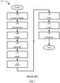
- Figure 1 is a process flow chart 100 showing certain steps of an example conventional process using a chromium based anodising process of the prior art for processing an aircraft part.
- a component is first cleaned and rinsed prior to processing.
- a deoxidising pre-treatment process will occur at step 104 prior to any anodising process to remove any existing oxide layer on the component surface.
- nitric and sulphuric acids may be applied to the component to deoxidise the surface in a redox reaction.
- the component is rinsed and dried to remove any remaining deoxidising substance form the surface of the component.
- the component is anodised in a chromic acid anodising solution, for example chromium trioxide.
- a chromic acid anodising solution for example chromium trioxide.
- the component may be dipped in a bath comprising the solution. Typically, this step of anodising the component may take about 1 hour.
- the anodised component is rinsed to remove any a residual anodising solution.
- Solvents or other cleaning chemicals may be used to remove remaining anodising solution and the component dried.
- the component is masked for painting such that the area to be exposed to the environment is left unmasked.
- Such masking may be performed using 3M 425 aluminium foil tape.
- such masking processes including cutting, making tape to a desired shape and applying the cut masking tape to the component may take about 3 hours.
- the component is painted.
- paint is only applied to unmasked areas of the component. Painting is typically carried out by spray techniques by a skilled operator taking care to overlap the spray sufficiently on the component without inducing dripping or running of the paint which would otherwise spoil the surface of the finished component. Typically, this step of painting the component may take about 3 hours.
- the paint is cured.
- the paint may be cured in air at room temperature or by addition of a catalyst or heat process.
- the component is de masked. Solvents or other cleaning chemicals may be used to remove any left over adhesive residue from the masking tape. Typically this stage may take about 1 hour.
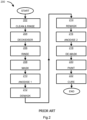
- Figure 2 is a process flow chart 200 showing certain steps of an example conventional process using an alternative to chromium based anodising processes of the prior art for processing an aircraft part using a two stage anodising process.
- step 202 to 206 are as steps 102 to 106 of Figure 1 .
- the component is masked such that a first area is exposed (unmasked) ready for a first anodising process, and a second area is a masked area ready to be anodised in the second stage of the process.
- Preparation of the masking materials and application to the component is similar to step 112 and takes about three hours.
- the component is anodised in a first anodising solution.
- the first anodising solution anodises the first area, to provide an improved surface for acceptance of a bonding agent, for example an adhesive, to a further component, such as a sub structure, for example, an aircraft spar.
- step 212 the second area of the component is demasked according to step 118 of Figure 1 .
- the first area of the component is masked such that the first area of step 208 is now completely covered thereby exposing the second area to be anodised in the second stage of the process.
- the component is anodised in a second anodising solution.
- the second anodising solution is selected to provide enhanced corrosion resistance to the second area of the component which in use, will be exposed to the environment, for example, the outer surface of an aircraft skin.
- the first area of the component is demasked according to step 118 of Figure 1 .
- Steps 220 and 222 are as steps 114 and 116 of Figure 1 .
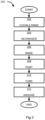
- Figure 3 shows an exemplary process 300 according to the invention for processing a component, in particular an aircraft part.
- the component is an aluminium aircraft aileron skin comprising a first and second area such that in use, the first area of the component will be will be exposed to the environment i.e., the outer skin of the aircraft, and the second area bonded to a substructure, for example an aircraft rib sub assembly.
- the method comprises the steps of; 302 cleaning and rinsing and component.
- the component is deoxidised with a sulphuric acid solution in order to strip the aluminium surface of the component from any existing oxide layer thereby ensuring consistent deposition of an oxide layer during the later anodising process.
- the component is rinsed and dried with water.
- the component is painted by selectively depositing an anodising resistant coating composition onto the first area of the component That is to say, the surface of the aluminium part to which the composition is applied will not react to form an oxide layer during the anodisation process.
- the anodising resistant coating composition is an epoxy urethane based composition applied by manual spraying.
- the component is cured under heat for 40 minutes at 150°C.
- the component is anodised in a phosphoric acid bath for 1 hour.
- Figure 4 shows an alternative exemplary process 400 according to the invention for processing a component using an electrophoretic deposition method.
- the component is as Figure 3 .
- the terms 'anionic' and 'cationic' are used, these are considered non limiting and any step comprising each term may be interchangeable providing subsequent steps are compatible.
- the electrodepositable coating composition is cationic vice versa in order to provide electrostatic attraction between the component and the coating composition.
- the component is cleaned and rinsed.
- cleaning may be carried out using mild or strong alkaline cleaners such as Chemkleen 163, Chemkleen 177 and Chemkleen 490MX which are commercially available from PPG Industries Ohio Inc.
- the cleaner may be removed from the component by a water based rinse.
- the component is deoxidised using a sulphuric acid solution.
- the component is cleaned with Chemkleen 163 before being rinsed under water.
- the second area of the component is masked with 3M 425 aluminium foil tape such that only the first area of the component will receive a coating compound during the electrophoretic deposition process. Even when a masking step is incorporated into the process, the time taken to process the component is still less than the process of Figure 2 as only one masking operating takes place as per Figure 1 .
- the component undergoes an electrophoretic pre rinse.
- the entire component is washed with a pre-treatment aqueous solution comprising a group IIIB metal and an electropositive metal.
- Said electropositive metal refers to metals that are more electropositive than the component to be processed. i.e. they are less easily oxidized than the component.
- the group IIIB metal is yttrium and the electropositive metal is copper sulfate.
- the pre-treatment metal may be present in the solution in the range of from 10ppm to 5000ppm.
- the entire component undergoes a cationic resin based post rinse process using Nupal 510 R.
- the first area of the component is coated with Aerocron TM 2100, an anodising resistant coating compound.
- the resultant thickness of the coating is in the range of from 10 to 50 microns.
- the specific voltages and amperes of the process will be determined by the skilled person according to the size, nature and complexity of the component and with regard to the specific coating composition being used including its conductivity and viscosity. As an example, a voltage applied in such process may be in the range of from 1 to 500 volts and a current in the range of from 10 to 160 amperes per square meter.
- the component is cured under heat for 40 minutes at 150°C.
- the component is de-masked.
- a solvent may be used to remove any exist ant adhesive residue left from the masking tape.
- the component is anodised.
- the component is immersed in a sulphuric acid bath for 1 hour.
- the cured coating composition provides an effective barrier to the acid, and prevents the formation of an oxide layer on the first area of the component.
- the cured coating composition effectively acting as a maskant against anodising.
- the second area only is anodised. Even when a masking step is incorporated into the process, the time taken to process the component is still less than the process of Figure 2 as only one masking operating takes place as per Figure 1 .
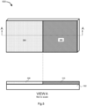
- Figure 5 shows a cross sectional view of a part processed aircraft part 500.
- an aluminium aircraft component 502 comprising a first area 504 and a second area 506.
- View A of Figure 5 shows a cross sectional view of the component showing discreet layers deposited on the component surface (not to scale).
- the component has undergone selective deposition of an anodising resistant coating composition and anodisation such that the first area 504 comprises a cured layer of cured epoxy urethane 508 and the second area 506 comprises an oxide layer 510 after anodisation.
- Figure 6 shows a cross sectional view of a fully processed aircraft part 600.
- an aluminium component 602 comprising a first area 604 and a second area 606.
- View B of Figure 6 shows a cross sectional view of the component showing discreet layers deposited on the component surface (not to scale).
- the component has undergone selective deposition of an anodising resistant coating composition and anodisation such that the first area 604 comprises a cured layer of cured epoxy urethane 608 and the second area 606 comprises an oxide layer 610 after anodisation.
- the first area 604 also comprises an epoxy based exterior coating composition comprising a pigment deposited on the surface of the cured epoxy urethane layer 608 such that the cured layer 608 effectively acts as a primer layer.
- the second area 606 further comprises a bonding primer in the form of Hysol TM deposited on the surface of the oxide layer 610.
- Figure 7 shows a fully processed aircraft part 700 in a final use location on an aircraft substructure.
- the component 702 is an aluminium aircraft skin comprising a first area 704 on a first side of the skin and a second area 706 on a second side of the skin, wherein the first area 704 comprises a layer of cured epoxy urethane 708 and a further layer of an epoxy based exterior coating composition 712.
- the second area 706 comprises an oxide layer 710, a bonding primer 714 deposited thereon wherein the component is joined to an adjacent component 716 by means of an adhesive.
Landscapes
- Chemical & Material Sciences (AREA)
- Engineering & Computer Science (AREA)
- Chemical Kinetics & Catalysis (AREA)
- Electrochemistry (AREA)
- Materials Engineering (AREA)
- Metallurgy (AREA)
- Organic Chemistry (AREA)
- Application Of Or Painting With Fluid Materials (AREA)
Abstract
A chromate free method of processing a component comprising a first and second area, the method comprising: selectively depositing a curable anodising resistant coating composition onto the first area of the component; curing the anodising resistant coating composition to create a cured anodising resistant coating layer; anodising the component with an anodising composition to create an anodised layer on the second area, such that the cured anodising resistant coating layer provides a maskant preventing anodisation of the first area.
Description
- The present invention relates to the processing of components.
- Many components, for example aircraft components such as panels, frames, ribs and spars etc., are painted.
- Aircraft components may comprise distinct areas which are subjected to different processes. One area of the component may be bonded to a separate sub structure, for example an internal frame and another area which is exposed to the environment, for example an outer surface of an aircraft part, may be painted with a coating compound. Typically, components are anodised for two reasons; firstly, to enhance the adhesion of bonding primers and agents, and secondly, to provide an oxide protective layer to increase corrosion resistance of the component. Areas of the component which are to be exposed to the environment are then painted with a coating compound. Anodising solutions which can provide both an enhanced bonding layer and corrosion resistance are typically hexavalent chromium based solutions, for example chromium trioxide (also known as chromium anhydride), and are compatible with existing aircraft paint systems however these anodising solutions are carcinogenic and are being phased out in many jurisdictions to comply with new health and safety legislation.
- It is an example aim of the present invention to at least partially solve or avoid one or more problems or disadvantages of processing a component, in particular components which must be anodised and painted to give enhanced corrosion resistance and bonding characteristics, using non carcinogenic materials.
- The present inventors have realised that alternative non-carcinogenic anodising solutions can neither provide both an enhanced bonding layer and corrosive resistance that is equivalent to the oxidising effects of a chromium based solution using a single process i.e. anodising the component only once with only one anodising solution. It is therefore necessary to use a two stage anodising process, wherein two separate anodising processes comprising two separate anodising solutions are used on a component. A first anodising process using a first anodising solution for an area to be bonded which provides an enhanced bonding layer and a second anodising process using a second anodising solution for an area to be exposed to the environment, which provides improved corrosion resistance. As such, it is necessary to mask a first area of the component, anodise the remaining exposed second area of the component with a first anodising solution, de-mask the first area of the component and remask the newly anodised second area of the component prior to anodising the first area of the component with a second anodising solution. In this way, equivalence in terms of quality of corrosion resistance and providing an enhanced bonding layer compared to chromium based solutions may be achieved. However the masking and de-masking process is a time consuming task for skilled operators and can often lead to under masking the first area such that there is anodising overlap resulting in pitting of the component or worse, over masking the first area such that there are missing areas of anodising on the component thus said missing areas will corrode quicker in use.
- The present inventors have realised that alternative anodising processes which do not use a chromic anodising solutions suffer from serious disadvantages such as an increase in process time (and therefore cost) due to the two stage anodising process and increased environmental waste from the resultant increase in masking consumables required during the process. The chromate process is desirable due to its efficient nature requiring only a single anodising process using only one anodising solution which provides both an enhanced bonding layer and corrosion resistance without the need to remask the component or use a separate second anodising process and associated anodising solution. However, as previously mentioned, the use of chromate is being phased out due to regulations of its use based on the toxicity and environmental impact of its use.
- The present inventors have realised there is an increased chance of quality defects in a processed part due to the possibility of an operator failing to correctly mask, and thereby overlap the two stage anodising process, increasing the possibility of creating pitting on the component surface or leaving gaps in anodising on parts of the component which may lead to early corrosion. The presence of defects may lead to rework of the component which involves having to strip the component back to the original surface and restart the entire process or even scrapping of the entire part. In the event of areas of the component not being anodised, especially in the case of an aircraft component, the component may have to be replaced early in its operational service.
- According to a first aspect of the present invention, there is provided a chromate free method of processing a component comprising a first and second area, the method comprising: selectively depositing a curable anodising resistant coating composition onto the first area of the component; curing the anodising resistant coating composition to create a cured anodising resistant coating layer; anodising the component with an anodising composition to create an anodised layer on the second area, such that the cured anodising resistant coating layer provides a maskant preventing anodisation of the first area.
- The process eliminates the need for a two stage anodising process. Therefore, the possibility of double anodising is mitigated thereby reducing significantly any chance of pitting as the cured anodising resistant coating layer acts as a maskant. The cured anodising resistant coating layer provides a suitable corrosion resistance barrier on the first area of the component.
- The component, which comprises the first and second area, is subjected to the anodising process. By both the first and second areas being subjected to the same anodising process, all areas which do not have the cured anodising resistant coating layer will be anodised. Therefore, the possibility of an area of the component not being subjected to anodising is mitigated. This significantly reduces the chance of a component being rejected for quality non-conformance as the entire area of the component, that is to say the first and second areas together, will either be coated in a cured anodising resistant coating layer (first area) or anodised (second area) therefore the component is entirely protected from corrosion.
- The process also reduces waste, as masking consumables are reduced or entirely eliminated altogether.
- The process requires less energy due to the elimination of the second stage anodising process.
- In the present invention, the component may be made of a metal, metal alloy or composite component.
- The component may be one used in a land, sea, space or air vehicle. Preferably, the component is an aerospace component. For example, the component may be an aircraft skin, panel or engine duct. Optionally, the component may be an internal component or a sub assembly, for example but not limited to, a spar, rib or bulkhead. More preferably, the component is a metal or composite aerospace component.
- Whilst the terms 'first area' and 'second area' have been used, these are considered non-limiting and merely indicate which area of the component is to be coated with an anodising resistant coating composition and which area is to be anodised. There may be more than one first or second area on the component. The first and second area may not be merely limited to respective sides of a component, for example there may be a plurality of 'first' areas on a first side of a component. Alternatively, the component may be of such a geometry that there are no defined 'sides', in such cases, the component surface may have a plurality of first and/or second areas.
- In one example, the component may be an aluminium aircraft aileron skin comprising a first and second area such that in use, the first area is an outer skin of the aircraft, which will be exposed to the environment. The second area is an inner surface of the aileron which is to be bonded to a substructure to form a sub assembly.
- In the present invention, the anodising resistant coating composition is selectively deposited on to the first area of the component. Such techniques may include painting using a brush, applicator, spraying, dipping, nozzle printing, electrostatic coating or electrophoretic deposition. Processes may be manual or automated, in this document manual meaning by hand. Automated processes may be partly or fully automated, for example, by a cobot or robot. Preferably, an electrophoretic deposition process is used to selectively deposit an anodising resistant coating composition onto the first area of the component.
- Where an electrophoretic deposition process is used, the component must be able to conduct a current. Non-conductive materials may be used providing they comprise some form of conductive element embedded within or located thereon, them, for example a metallic layer, metallic seed layer or an interwoven conductive material, for example within a composite. Alternatively, a non conductive material, for example a carbon fibre composite, which comprises a non-conductive binder matrix, may comprise an external conductive layer, for example, an aluminium layer.
- Selective deposition may include depositing the anodising resistant coating composition onto a discreet region of a component, such as the first area, that is to say, without traditional masking techniques. For example, the anodising resistant coating composition may be selectively deposited by a printing process onto the first area of the component leaving the remainder of the component uncoated. In an alternative process, the component' first area may be partly dipped in an anodising resistant coating composition thereby leaving the undipped surface of the second area of the component uncoated. Alternatively, selective deposition may be achieved through traditional masking techniques applied to mask the second area such that selective deposition is applied to only the first area of the component. The unmasked first area therefore receives a deposited layer of anodising resistant coating composition.
- An electrophoretic deposition process yields a uniform, i.e. an even thickness of anodising resistant coating composition across the first area of the component.
- Preferably, the resultant thickness of the coating is in the range of from 1 to 500 microns, more preferably 10 to 100 microns, more preferably 10 to 50microns.
- The anodising resistant coating composition may be an organic or inorganic composition. The anodising resistant coating composition may comprise a film- forming resin. The term "film-forming resin" refers to resins that can form a self-supporting continuous film on at least a horizontal surface of a substrate upon removal of any diluents or carriers present in the composition or upon curing at ambient or elevated temperature. The anodising resistant coating composition may comprise a thermosetting film-forming resin, said resin may be cured or set irreversibly upon curing, for example by undergoing a process such as crosslinking.
- Preferably, anodising resistant coating composition may be an ionic electrodepositable composition, such as an anionic or cationic electrodepositable composition.
- The ionic electrodepositable composition may be water dispersible polymers. Examples of ionic electrodepositable composition may be base-solubilised, carboxylic acid containing polymers, neutralized interpolymers of hydroxyl-alkyl esters of unsatured carboxylic acids, unsaturated carboxylic acid and at least one other ethlenically unsaturated monomer, mixed esters of a resinous polyol as described in
US3749657 incorporated herein by reference, phosphatised polyepoxide or phosphatised acrylic polymers. - Preferably, the anodising resistant coating composition may be an epoxy or an epoxyurethane based composition. The anodising resistant coating composition may be an anionic epoxy electrocoat primer based composition.
- The present inventors have found that Aerocron™ 2100 anionic epoxy electrocoat primer as manufactured by PPG Industries Ohio Inc is particularly effective in providing an anodising resistant coating to the component.
- The anodising resistant coating composition may comprise a curing agent. For example, the curing agent may be a blocked organic polyisocyanate or aminoplast.
- The anodising resistant coating composition may comprise a filler or a plurality of fillers. Such fillers may be dyes, pigments, stabilisers or a property inducing filler, for example a magnetic filler.
- In a highly preferred arrangement the anodising resistant coating composition may be applied by the electrophoretic deposition process as per
WO2013089903A1 by PPG Industries Ohio Inc, incorporated herein by reference. - Optionally, the method may comprise the intermediate step of contacting the component with a pre-treatment solution before electrophoretic deposition. The pre-treatment solution may comprise a group IIIB and/or IVB metal. Such pre-treatment may provide a protective layer on the surface of the component.
- Optionally, the method may also comprise the intermediate step of contacting the component with an anionic or cationic resin-based post rinse composition comprising an anionic or cationic resin before electrophoretic deposition. The addition of this step increases the 'throwpower' of the subsequently applied electrodeposition coating. In this document. 'Throwpower' means the ability of the electrodeposited coating to be 'thrown' into component recesses and hard to reach geometries. An increased throwpower of the electrodeposited coating therefore means a more even coat thickness across the entire surface of the component thus there is provided a uniform finish on the part.
- After electrophoretic deposition, the component may be cured. The curing process may take place in the presence of a catalyst, for example heat or UV. Preferably the component is cured by heating at a temperature in the range of from 120°C to 250°C. More preferably, the component is cured at a temperature in the range of from 120°C to 190°C. Where the component is cured by heating, the curing time of the cure may be in the range of from 10 to 60 minutes.
- After application and subsequent curing of the anodising resistant coating composition to the first area of the component, the second area of the component is then anodised. The anodising composition may be any known suitable agent, and may be selected from an acid such as for example an acidic composition, one comprising phosphoric acid or sulphuric acid. Preferably, the anodising solution is sulphuric acid. Such selection of anodising solutions will be compliant with local legal requirements, such as the Registration Evaluation Authorisation and Restriction of Chemicals (REACH) regulation of the European Union.
- The cured anodising resistant coating layer prevents the first area of the component from being anodised as it is impermeable to anodisation, such that the underlying surface of the first area of the component does not form an oxide layer. Therefore, only the second area, which has no cured anodising resistant coating layer is subjected to anodisation to form an oxide layer thereon.
- In an alternative arrangement, the method may also comprise the additional step of masking the second area of the component before depositing the anodising resistant coating composition onto the entire component. The anodising resistant coating composition is cured. The mask is then removed from the second area and subjected to anodising. This additional step allows the entire component to be exposed to the electrophoretic deposition process and then removal of the mask on the second area to perform the anodising process, rather than selectively applying each process to the first and second area of the component respectively. Such masking may be performed using 3M 425 aluminium foil tape.
- As a yet further alternative, the component, that is to say the first and second areas, are both subjected to deposition with an anodising resistant coating composition; whereupon the second area which is to be anodised, has the anodising resistant coating composition removed or "stripped back" to the second area's original surface before undergoing an anodising process. Such stripping back may be achieved with use of a solvent, physical abrasive or in any other way known by the skilled person. Where the second area is difficult to mask, or where there is only a small surface area of second area, it may be convenient to use the stripped back process.
- To improve bonding with the anodised surface, the method may further comprise the step of applying a bonding primer to the second area of the component after anodising. The bonding primer may be selected from a group comprising EC3900, BR127 or non chromate BR6747 as produced by Solvay Group®. Preferably the bonding primer is non-chromate BR6747 as this primer is REACH compliant. The bonding primer may enhance the adhesion of a bonding layer or secondary paint layer onto the component. The bonding primer may be applied to the second area of the component by manual painting, manual spraying, robotic spraying, dipping or electrostatic coating or in any other known way by the skilled person.
- The method may comprise the additional step of bonding the second area of the component to a further component. Optionally, with the use of a bonding primer. A further component may be another component as herein defined. For example, the further component may be bonded to a substructure, for example an aircraft rib or spar. The bonding may include the use of adhesives, such as, for example Hysol™ as produced by Henkel®. Alternatively, the second area may be joined to another component by mechanical means, for example rivets, welds, and/or bolts.
- Optionally, the method comprises the additional step of applying an exterior coating composition to the first area of the component. For example, the exterior coating may be a final finish paint which in use, will be exposed to the outer environment. The exterior coating composition may be an epoxy or epoxy polyurethane based composition. The exterior coating composition may comprise more than one discreet layer of composition, for example the composition may be layered as; primer - intermediate layer - top coat as part of a paint system. This arrangement eases stripping of the top coat for repaint which may be especially useful on an aerospace component. The exterior coating composition may comprise a filler or a plurality of fillers. Such fillers may be dyes, pigments, stabilisers or a property inducing filler, for example a magnetic filler. Preferably, the exterior coating is an epoxy polyurethane based composition. Preferably the exterior coating may be applied directly to the cured anodising resistant coating layer.
- According to a second aspect of the invention, there is provided a processed component comprising: a first area; and, a second area, wherein the first area comprises an anodising resistant coating composition and the second area comprises an anodised layer.
- Optionally, the first area may comprise an exterior coating composition deposited on the cured anodising resistant coating layer.
- Optionally the second area may also comprise a bonding primer deposited on the surface of the anodised layer.
- The processed component may be part of an aircraft, for example an aircraft panel.
- According to a third aspect of the invention, there is provided a chromate free method of processing a component, the method comprising:
- masking a second area of the component wherein the second area is an area to be anodised;
- electrophoretically depositing an anodising resistant electodepositable coating composition onto a first area of the component to create a electrodeposited coating layer;
- curing the electrodeposited coating layer to create a cured electrodeposited coating layer;
- demasking the second area of the component;
- anodising the component with an anodising composition to create an anodised layer on the second area wherein the cured electrodeposited coating layer provides a maskant preventing anodisation of the first area.
- Embodiments of the invention will now be described by way of example only with reference to the figures, in which:
-
Figure 1 shows an example of a conventional process using a chromium based anodising process of the prior art for processing an aircraft part. -
Figure 2 shows an example of a conventional process using an alternative to chromium based anodising processes of the prior art for processing an aircraft part using a two stage anodising process. -
Figure 3 shows an exemplary process according to the invention of processing an aircraft part. -
Figure 4 shows an alternative exemplary process according to the invention of processing an aircraft part using an electrophoretic deposition process. -
Figure 5 shows a cross sectional view of a part processed aircraft part. -
Figure 6 shows a cross sectional view of a fully processed aircraft part. -
Figure 7 shows a fully processed aircraft part in a final use location on an aircraft substructure. -
Figure 1 is aprocess flow chart 100 showing certain steps of an example conventional process using a chromium based anodising process of the prior art for processing an aircraft part. - At
step 102, a component is first cleaned and rinsed prior to processing. Typically a deoxidising pre-treatment process will occur atstep 104 prior to any anodising process to remove any existing oxide layer on the component surface. Typically, nitric and sulphuric acids may be applied to the component to deoxidise the surface in a redox reaction. - At
step 106, the component is rinsed and dried to remove any remaining deoxidising substance form the surface of the component. - At
step 108, the component is anodised in a chromic acid anodising solution, for example chromium trioxide. The component may be dipped in a bath comprising the solution. Typically, this step of anodising the component may take about 1 hour. - At
step 110, the anodised component is rinsed to remove any a residual anodising solution. Solvents or other cleaning chemicals may be used to remove remaining anodising solution and the component dried. - At
step 112, the component is masked for painting such that the area to be exposed to the environment is left unmasked. Such masking may be performed using 3M 425 aluminium foil tape. Typically, such masking processes, including cutting, making tape to a desired shape and applying the cut masking tape to the component may take about 3 hours. - At
step 114, the component is painted. In this example, paint is only applied to unmasked areas of the component. Painting is typically carried out by spray techniques by a skilled operator taking care to overlap the spray sufficiently on the component without inducing dripping or running of the paint which would otherwise spoil the surface of the finished component. Typically, this step of painting the component may take about 3 hours. - At
step 116, the paint is cured. In this example the paint may be cured in air at room temperature or by addition of a catalyst or heat process. - At
step 118, the component is de masked. Solvents or other cleaning chemicals may be used to remove any left over adhesive residue from the masking tape. Typically this stage may take about 1 hour. - Thus an example conventional process for processing a component using a chromium based anodising process is provided.
-
Figure 2 is aprocess flow chart 200 showing certain steps of an example conventional process using an alternative to chromium based anodising processes of the prior art for processing an aircraft part using a two stage anodising process. - At
step 202 to 206 are assteps 102 to 106 ofFigure 1 . - At step 208, the component is masked such that a first area is exposed (unmasked) ready for a first anodising process, and a second area is a masked area ready to be anodised in the second stage of the process. Preparation of the masking materials and application to the component is similar to step 112 and takes about three hours.
- At
step 210, the component is anodised in a first anodising solution. The first anodising solution anodises the first area, to provide an improved surface for acceptance of a bonding agent, for example an adhesive, to a further component, such as a sub structure, for example, an aircraft spar. - At
step 212, the second area of the component is demasked according to step 118 ofFigure 1 . - At
step 214, the first area of the component is masked such that the first area of step 208 is now completely covered thereby exposing the second area to be anodised in the second stage of the process. - At
step 216, the component is anodised in a second anodising solution. The second anodising solution is selected to provide enhanced corrosion resistance to the second area of the component which in use, will be exposed to the environment, for example, the outer surface of an aircraft skin. - At
step 218, the first area of the component is demasked according to step 118 ofFigure 1 . -
Steps steps Figure 1 . - Thus an example conventional process for processing a component using a two stage anodising process with an alternative to chromium based anodising solutions is provided.
-
Figure 3 shows anexemplary process 300 according to the invention for processing a component, in particular an aircraft part. In this example the component is an aluminium aircraft aileron skin comprising a first and second area such that in use, the first area of the component will be will be exposed to the environment i.e., the outer skin of the aircraft, and the second area bonded to a substructure, for example an aircraft rib sub assembly. The method comprises the steps of; 302 cleaning and rinsing and component. Atstep 304, the component is deoxidised with a sulphuric acid solution in order to strip the aluminium surface of the component from any existing oxide layer thereby ensuring consistent deposition of an oxide layer during the later anodising process. Atstep 306, the component is rinsed and dried with water. - At step 308, the component is painted by selectively depositing an anodising resistant coating composition onto the first area of the component That is to say, the surface of the aluminium part to which the composition is applied will not react to form an oxide layer during the anodisation process. The anodising resistant coating composition is an epoxy urethane based composition applied by manual spraying.
- At
step 310, the component is cured under heat for 40 minutes at 150°C. - At
step 312, the component is anodised in a phosphoric acid bath for 1 hour. -
Figure 4 shows an alternative exemplary process 400 according to the invention for processing a component using an electrophoretic deposition method. In this process, the component is asFigure 3 . In this process where the terms 'anionic' and 'cationic' are used, these are considered non limiting and any step comprising each term may be interchangeable providing subsequent steps are compatible. For example, where an anionic post rinse composition is used on a component, the electrodepositable coating composition is cationic vice versa in order to provide electrostatic attraction between the component and the coating composition. - At
step 402 the component is cleaned and rinsed. Such cleaning may be carried out using mild or strong alkaline cleaners such as Chemkleen 163, Chemkleen 177 and Chemkleen 490MX which are commercially available from PPG Industries Ohio Inc. The cleaner may be removed from the component by a water based rinse. - At
step 404, the component is deoxidised using a sulphuric acid solution. - At
step 406, the component is cleaned with Chemkleen 163 before being rinsed under water. - At step 408, the second area of the component is masked with 3M 425 aluminium foil tape such that only the first area of the component will receive a coating compound during the electrophoretic deposition process. Even when a masking step is incorporated into the process, the time taken to process the component is still less than the process of
Figure 2 as only one masking operating takes place as perFigure 1 . - At
step 410, the component undergoes an electrophoretic pre rinse. In this example, the entire component is washed with a pre-treatment aqueous solution comprising a group IIIB metal and an electropositive metal. Said electropositive metal refers to metals that are more electropositive than the component to be processed. i.e. they are less easily oxidized than the component. In this example, the group IIIB metal is yttrium and the electropositive metal is copper sulfate. The pre-treatment metal may be present in the solution in the range of from 10ppm to 5000ppm. - At
step 412, the entire component undergoes a cationic resin based post rinse process using Nupal 510 R. - At
step 414, the first area of the component is coated with Aerocron™ 2100, an anodising resistant coating compound. Preferably, the resultant thickness of the coating is in the range of from 10 to 50 microns. The specific voltages and amperes of the process will be determined by the skilled person according to the size, nature and complexity of the component and with regard to the specific coating composition being used including its conductivity and viscosity. As an example, a voltage applied in such process may be in the range of from 1 to 500 volts and a current in the range of from 10 to 160 amperes per square meter. - At
step 416, the component is cured under heat for 40 minutes at 150°C. - At
step 418, the component is de-masked. A solvent may be used to remove any exist ant adhesive residue left from the masking tape. - At
step 420, the component is anodised. The component is immersed in a sulphuric acid bath for 1 hour. At this stage, the cured coating composition provides an effective barrier to the acid, and prevents the formation of an oxide layer on the first area of the component. The cured coating composition effectively acting as a maskant against anodising. The second area only is anodised. Even when a masking step is incorporated into the process, the time taken to process the component is still less than the process ofFigure 2 as only one masking operating takes place as perFigure 1 . -
Figure 5 shows a cross sectional view of a part processedaircraft part 500. In this example, there is provided analuminium aircraft component 502 comprising afirst area 504 and asecond area 506. View A ofFigure 5 shows a cross sectional view of the component showing discreet layers deposited on the component surface (not to scale). In this example, the component has undergone selective deposition of an anodising resistant coating composition and anodisation such that thefirst area 504 comprises a cured layer of curedepoxy urethane 508 and thesecond area 506 comprises anoxide layer 510 after anodisation. -
Figure 6 shows a cross sectional view of a fully processedaircraft part 600. In this example, there is provided analuminium component 602 comprising afirst area 604 and a second area 606. View B ofFigure 6 shows a cross sectional view of the component showing discreet layers deposited on the component surface (not to scale). In this example, the component has undergone selective deposition of an anodising resistant coating composition and anodisation such that thefirst area 604 comprises a cured layer of curedepoxy urethane 608 and the second area 606 comprises anoxide layer 610 after anodisation. In addition, thefirst area 604 also comprises an epoxy based exterior coating composition comprising a pigment deposited on the surface of the curedepoxy urethane layer 608 such that the curedlayer 608 effectively acts as a primer layer. In addition, the second area 606 further comprises a bonding primer in the form of Hysol™ deposited on the surface of theoxide layer 610. -
Figure 7 shows a fully processedaircraft part 700 in a final use location on an aircraft substructure. In this example, thecomponent 702 is an aluminium aircraft skin comprising afirst area 704 on a first side of the skin and asecond area 706 on a second side of the skin, wherein thefirst area 704 comprises a layer of curedepoxy urethane 708 and a further layer of an epoxy basedexterior coating composition 712. Thesecond area 706 comprises anoxide layer 710, abonding primer 714 deposited thereon wherein the component is joined to anadjacent component 716 by means of an adhesive.
Claims (17)
- A chromate free method of processing a component comprising a first and second area, the method comprising:selectively depositing a curable anodising resistant coating composition onto the first area of the component;curing the anodising resistant coating composition to create a cured anodising resistant coating layer;anodising the component with an anodising composition to create an anodised layer on the second area, such that the cured anodising resistant coating layer provides a maskant preventing anodisation of the first area.
- The method of processing a component according to claim 1 wherein the step of depositing the anodising resistant coating composition is carried out by an electrophoretic deposition process.
- The method of processing a component according to any preceding claim further comprising the additional step of masking the second area of the component before depositing the anodising resistant coating composition onto the first area component.
- The method of processing a component according to claim 2 or 3, the method further comprising the intermediate step of contacting the first area with a pre-treatment solution before electrophoretic deposition.
- The method of processing a component according to claim 4 wherein the pre-treatment solution comprises a group IIIB metal and/or a group IVB metal and an electropositive metal.
- The method of processing a component according to any preceding claim, the method further comprising the intermediate step of contacting the component with an anionic or cationic resin-based post rinse composition.
- The method of processing a component according to claim 2 to 6 wherein the anodic resistant electrodepositable coating composition is an inorganic composition or organic composition.
- The method of processing a component according to claim 7 wherein the anodic resistant electrodepositable coating composition is an epoxy or epoxyurethane.
- The method of processing a component according to any preceding claim wherein the anodising composition is selected from a group comprising chromic acid, phosphoric acid or sulphuric acid.
- The method of processing a component according to any preceding claim, the method further comprising the step of applying a bonding primer to the first area of the component after anodising.
- The method of processing a component according to claim 10 wherein the method comprises the additional step of bonding the second area of the component to a further component.
- The method of processing a component according to any preceding claim wherein the method comprises the additional step of applying an exterior coating composition to the first area of the component.
- The method of processing a component according to any preceding claim wherein the component and/or the further component are independently selected from a metal, metal alloy or composite component.
- The method of processing a component according to any preceding claim wherein the component and/or the further component are aerospace components.
- A processed component comprising:a first area; and,a second area,wherein the first area comprises an anodising resistant coating composition and the second area comprises an anodised surface .
- A processed component according to claim 15 wherein the component being at least part of an aircraft.
- A chromate free method of processing a component, the method comprising:masking a second area of the component wherein the second area is an area to be anodised;electrophoretically depositing an anodising resistant electodepositable coating composition onto a first area of the component to create a electrodeposited coating layer;curing the electrodeposited coating layer to create a cured electrodeposited coating layer;demasking the second area of the component;anodising the component with an anodising composition to create an anodised layer on the second area wherein the cured electrodeposited coating layer provides a maskant preventing anodisation of the first area.
Priority Applications (1)
| Application Number | Priority Date | Filing Date | Title |
|---|---|---|---|
| EP21275169.7A EP4187000A1 (en) | 2021-11-25 | 2021-11-25 | Component processing |
Applications Claiming Priority (1)
| Application Number | Priority Date | Filing Date | Title |
|---|---|---|---|
| EP21275169.7A EP4187000A1 (en) | 2021-11-25 | 2021-11-25 | Component processing |
Publications (1)
| Publication Number | Publication Date |
|---|---|
| EP4187000A1 true EP4187000A1 (en) | 2023-05-31 |
Family
ID=78806436
Family Applications (1)
| Application Number | Title | Priority Date | Filing Date |
|---|---|---|---|
| EP21275169.7A Pending EP4187000A1 (en) | 2021-11-25 | 2021-11-25 | Component processing |
Country Status (1)
| Country | Link |
|---|---|
| EP (1) | EP4187000A1 (en) |
Citations (6)
| Publication number | Priority date | Publication date | Assignee | Title |
|---|---|---|---|---|
| US3749657A (en) | 1972-01-04 | 1973-07-31 | Ppg Industries Inc | Treatment of electrodeposition rinse water |
| US20130153428A1 (en) * | 2011-12-20 | 2013-06-20 | Apple Inc. | Metal Surface and Process for Treating a Metal Surface |
| WO2013089903A1 (en) | 2011-12-13 | 2013-06-20 | Ppg Industries Ohio, Inc. | Resin based post rinse for improved throwpower of electrodepositable coating compositions on pretreated metal substrates |
| US20170226650A1 (en) * | 2016-02-04 | 2017-08-10 | Xiaojiang Zhang | Metallic picture print with the use of differentially oxidized and/or nitridized layers, and method for making the same |
| US20170342587A1 (en) * | 2014-12-17 | 2017-11-30 | Bae Systems Plc | Object processing by conversion coating |
| EP3399851A1 (en) * | 2015-12-30 | 2018-11-07 | BYD Company Limited | Aluminum alloy housing and preparation method thereof |
-
2021
- 2021-11-25 EP EP21275169.7A patent/EP4187000A1/en active Pending
Patent Citations (6)
| Publication number | Priority date | Publication date | Assignee | Title |
|---|---|---|---|---|
| US3749657A (en) | 1972-01-04 | 1973-07-31 | Ppg Industries Inc | Treatment of electrodeposition rinse water |
| WO2013089903A1 (en) | 2011-12-13 | 2013-06-20 | Ppg Industries Ohio, Inc. | Resin based post rinse for improved throwpower of electrodepositable coating compositions on pretreated metal substrates |
| US20130153428A1 (en) * | 2011-12-20 | 2013-06-20 | Apple Inc. | Metal Surface and Process for Treating a Metal Surface |
| US20170342587A1 (en) * | 2014-12-17 | 2017-11-30 | Bae Systems Plc | Object processing by conversion coating |
| EP3399851A1 (en) * | 2015-12-30 | 2018-11-07 | BYD Company Limited | Aluminum alloy housing and preparation method thereof |
| US20170226650A1 (en) * | 2016-02-04 | 2017-08-10 | Xiaojiang Zhang | Metallic picture print with the use of differentially oxidized and/or nitridized layers, and method for making the same |
Non-Patent Citations (1)
| Title |
|---|
| KERN P ET AL: "New developments in through-mask electrochemical micromachining of titanium", JOURNAL OF MICROMECHANICS AND MICROENGINEERING, INSTITUTE OF PHYSICS PUBLISHING, BRISTOL, GB, vol. 17, no. 6, 1 June 2007 (2007-06-01), pages 1168 - 1177, XP020120121, ISSN: 0960-1317, DOI: 10.1088/0960-1317/17/6/010 * |
Similar Documents
| Publication | Publication Date | Title |
|---|---|---|
| DE112009001005B4 (en) | A method of protecting an article against corrosion and a method of protecting a magnesium surface | |
| EP1280865A1 (en) | Conductive organic coatings | |
| US4274887A (en) | Lacquer coated metal surface | |
| US6872294B2 (en) | Metallization of polymer composite parts for painting | |
| DE102012213455B4 (en) | Process for forming an anti-corrosion layer on the surface of a CFRP component | |
| DE2114615A1 (en) | Process for the corrosion protection of sheet metal parts of vehicle superstructures and floor assemblies n | |
| GB2613173A (en) | Component processing | |
| DE102009051899B3 (en) | Component, useful as structural component of motor vehicles, preferably e.g. body framework structure, comprises a zinc lamella layer and a coating exhibiting lacquer layer, where the zinc lamella layer is applied on the lacquer layer | |
| CN109750341B (en) | Method for coating a body-in-white structure comprising an aluminium alloy on at least one surface | |
| DE19716234A1 (en) | Multilayer coating process for automobile parts and bodies | |
| WO2024188528A1 (en) | Method for producing a structural adhesive connection and method for releasing a structural adhesive connection | |
| US12595873B2 (en) | Electrolytic coating for aluminum components with weld joints | |
| DE10028705B4 (en) | Method for producing a body element of a motor vehicle coated with at least two different paints | |
| DE2056676A1 (en) | Car body parts - corrosion-proofed by surface treatment before and after assembly | |
| DE2263038C3 (en) | Process for coating aluminum or aluminum alloy material | |
| DE19534898A1 (en) | Electrophoretic dip lacquering of plastic substrates, for automobile work | |
| EP3368272B1 (en) | Metal-plastic composite element and method for manufacturing such a composite element | |
| US20240009700A1 (en) | Process for protecting an aluminum alloy part | |
| JP3991923B2 (en) | Painting method | |
| US7101589B1 (en) | Magnesium corrosion protection with adhesion promoter | |
| JP4299939B2 (en) | Car body coating method | |
| JP4339479B2 (en) | Car body coating method | |
| SE526172C2 (en) | Method of treating a surface | |
| EP1658904A1 (en) | Method and apparatus for varnishing work pieces | |
| DE102010047197A1 (en) | Corrosion-prone material made work piece for use during manufacture of motor vehicle e.g. car, has protection layer whose edge portions are coated with physical vapor deposition coating |
Legal Events
| Date | Code | Title | Description |
|---|---|---|---|
| PUAI | Public reference made under article 153(3) epc to a published international application that has entered the european phase |
Free format text: ORIGINAL CODE: 0009012 |
|
| STAA | Information on the status of an ep patent application or granted ep patent |
Free format text: STATUS: THE APPLICATION HAS BEEN PUBLISHED |
|
| AK | Designated contracting states |
Kind code of ref document: A1 Designated state(s): AL AT BE BG CH CY CZ DE DK EE ES FI FR GB GR HR HU IE IS IT LI LT LU LV MC MK MT NL NO PL PT RO RS SE SI SK SM TR |