EP4184745B1 - Data line and charging device - Google Patents
Data line and charging device Download PDFInfo
- Publication number
- EP4184745B1 EP4184745B1 EP21841700.4A EP21841700A EP4184745B1 EP 4184745 B1 EP4184745 B1 EP 4184745B1 EP 21841700 A EP21841700 A EP 21841700A EP 4184745 B1 EP4184745 B1 EP 4184745B1
- Authority
- EP
- European Patent Office
- Prior art keywords
- pin
- type
- interface
- circuit
- terminal
- Prior art date
- Legal status (The legal status is an assumption and is not a legal conclusion. Google has not performed a legal analysis and makes no representation as to the accuracy of the status listed.)
- Active
Links
Images


Classifications
-
- G—PHYSICS
- G06—COMPUTING OR CALCULATING; COUNTING
- G06F—ELECTRIC DIGITAL DATA PROCESSING
- G06F13/00—Interconnection of, or transfer of information or other signals between, memories, input/output devices or central processing units
- G06F13/38—Information transfer, e.g. on bus
- G06F13/40—Bus structure
- G06F13/4063—Device-to-bus coupling
- G06F13/4068—Electrical coupling
-
- G—PHYSICS
- G05—CONTROLLING; REGULATING
- G05F—SYSTEMS FOR REGULATING ELECTRIC OR MAGNETIC VARIABLES
- G05F1/00—Automatic systems in which deviations of an electric quantity from one or more predetermined values are detected at the output of the system and fed back to a device within the system to restore the detected quantity to its predetermined value or values, i.e. retroactive systems
- G05F1/10—Regulating voltage or current
- G05F1/46—Regulating voltage or current wherein the variable actually regulated by the final control device is DC
- G05F1/56—Regulating voltage or current wherein the variable actually regulated by the final control device is DC using semiconductor devices in series with the load as final control devices
-
- G—PHYSICS
- G06—COMPUTING OR CALCULATING; COUNTING
- G06F—ELECTRIC DIGITAL DATA PROCESSING
- G06F13/00—Interconnection of, or transfer of information or other signals between, memories, input/output devices or central processing units
- G06F13/38—Information transfer, e.g. on bus
- G06F13/382—Information transfer, e.g. on bus using universal interface adapter
-
- G—PHYSICS
- G06—COMPUTING OR CALCULATING; COUNTING
- G06F—ELECTRIC DIGITAL DATA PROCESSING
- G06F13/00—Interconnection of, or transfer of information or other signals between, memories, input/output devices or central processing units
- G06F13/38—Information transfer, e.g. on bus
- G06F13/42—Bus transfer protocol, e.g. handshake; Synchronisation
- G06F13/4282—Bus transfer protocol, e.g. handshake; Synchronisation on a serial bus, e.g. I2C bus, SPI bus
-
- H—ELECTRICITY
- H01—ELECTRIC ELEMENTS
- H01R—ELECTRICALLY-CONDUCTIVE CONNECTIONS; STRUCTURAL ASSOCIATIONS OF A PLURALITY OF MUTUALLY-INSULATED ELECTRICAL CONNECTING ELEMENTS; COUPLING DEVICES; CURRENT COLLECTORS
- H01R13/00—Details of coupling devices of the kinds covered by groups H01R12/70 or H01R24/00 - H01R33/00
- H01R13/66—Structural association with built-in electrical component
- H01R13/665—Structural association with built-in electrical component with built-in electronic circuit
- H01R13/6691—Structural association with built-in electrical component with built-in electronic circuit with built-in signalling means
-
- H—ELECTRICITY
- H01—ELECTRIC ELEMENTS
- H01R—ELECTRICALLY-CONDUCTIVE CONNECTIONS; STRUCTURAL ASSOCIATIONS OF A PLURALITY OF MUTUALLY-INSULATED ELECTRICAL CONNECTING ELEMENTS; COUPLING DEVICES; CURRENT COLLECTORS
- H01R24/00—Two-part coupling devices, or either of their cooperating parts, characterised by their overall structure
- H01R24/60—Contacts spaced along planar side wall transverse to longitudinal axis of engagement
-
- H—ELECTRICITY
- H02—GENERATION; CONVERSION OR DISTRIBUTION OF ELECTRIC POWER
- H02J—ELECTRIC POWER NETWORKS; CIRCUIT ARRANGEMENTS OR SYSTEMS FOR SUPPLYING OR DISTRIBUTING ELECTRIC POWER; SYSTEMS FOR STORING ELECTRIC ENERGY
- H02J7/00—Circuit arrangements for charging or discharging batteries or for supplying loads from batteries
- H02J7/40—Circuit arrangements for charging or discharging batteries or for supplying loads from batteries characterised by the exchange of charge or discharge related data
- H02J7/47—Arrangements for checking compatibility or authentication between one component, e.g. a battery or a battery charger, and another component, e.g. a power source
-
- G—PHYSICS
- G06—COMPUTING OR CALCULATING; COUNTING
- G06F—ELECTRIC DIGITAL DATA PROCESSING
- G06F2213/00—Indexing scheme relating to interconnection of, or transfer of information or other signals between, memories, input/output devices or central processing units
- G06F2213/0042—Universal serial bus [USB]
-
- H—ELECTRICITY
- H02—GENERATION; CONVERSION OR DISTRIBUTION OF ELECTRIC POWER
- H02J—ELECTRIC POWER NETWORKS; CIRCUIT ARRANGEMENTS OR SYSTEMS FOR SUPPLYING OR DISTRIBUTING ELECTRIC POWER; SYSTEMS FOR STORING ELECTRIC ENERGY
- H02J2207/00—Details of circuit arrangements for charging or discharging batteries or supplying loads from batteries
- H02J2207/30—Charge provided using DC bus or data bus of a computer
-
- Y—GENERAL TAGGING OF NEW TECHNOLOGICAL DEVELOPMENTS; GENERAL TAGGING OF CROSS-SECTIONAL TECHNOLOGIES SPANNING OVER SEVERAL SECTIONS OF THE IPC; TECHNICAL SUBJECTS COVERED BY FORMER USPC CROSS-REFERENCE ART COLLECTIONS [XRACs] AND DIGESTS
- Y02—TECHNOLOGIES OR APPLICATIONS FOR MITIGATION OR ADAPTATION AGAINST CLIMATE CHANGE
- Y02D—CLIMATE CHANGE MITIGATION TECHNOLOGIES IN INFORMATION AND COMMUNICATION TECHNOLOGIES [ICT], I.E. INFORMATION AND COMMUNICATION TECHNOLOGIES AIMING AT THE REDUCTION OF THEIR OWN ENERGY USE
- Y02D10/00—Energy efficient computing, e.g. low power processors, power management or thermal management
Definitions
- This application pertains to the field of communication technologies, and specifically relates to a data cable and a charging device.
- a power delivery (Power Delivery, PD) protocol is generally used for quick charging.
- a charger that supports charging of the PD protocol needs to use a configuration channel (Configuration Channel, CC) signal cable for communication.
- the charger that supports charging of the PD protocol generally uses a type-C (Type-C) interface and has a Type-C to Type-C data cable.
- a data cable that uses a type-A (Type-A or Standard-A) interface performs communication by using a D+/D-signal cable, and cannot support charging in the PD protocol. Therefore, a type-A interface on the data cable does not support charging in the PD protocol.
- Embodiments of this application are to provide a data cable and a charging device, which can resolve a problem that a data cable with a type-A interface does not support charging in a PD protocol.
- an embodiment of this application provides a data cable, including: a type-A interface and a type-C interface, where the type-A interface and the type-C interface are connected by using a cable, the type-A interface and the type-C interface each have a VBUS pin, a CC pin, a D+ pin, a D- pin, and a GND pin, and a VBUS pin, a D+ pin, a D- pin, and a GND pin of the type-A interface are connected to a VBUS pin, a D+ pin, a D- pin, and a GND pin of the type-C interface, respectively;
- an embodiment of this application provides a charging device, including a data cable and a charger.
- the data cable is the data cable in the first aspect
- the charger includes a PD charging processing module, and when the charger is connected to the data cable, the PD charging processing module is connected to the CC pin in the type-A interface.
- a CC pin is disposed in a type-A interface of a data cable, a CC communication signal transmitted on the CC pin of the type-A interface is filtered into a stable control signal by using a filtering circuit, and a comparator circuit is used to compare the analog signal with a stable voltage provided by a voltage regulator circuit, to output a corresponding control signal, so that when there is a signal on the CC pin of the type-A interface and when there is no signal on the CC pin of the type-A interface, control signals output by the comparator circuit are different control signals; an on/off state of a switch circuit is controlled according to the control signal, so that when the switch circuit connects an output terminal of the voltage regulator circuit to a CC pin of a type-C interface, the data cable can only perform non-PD protocol communication by using a D+ pin and a D- pin; and when the switch circuit connects the CC pin of the type-A interface to the CC pin of the type-C interface, the data cable can can
- first and second in the specification and claims of this application are used to distinguish between similar objects, and do not need to be used to describe a specific order or sequence. It should be understood that data used in this way may be interchangeable in an appropriate case, so that the embodiments of this application can be implemented in a sequence other than those shown or described herein, and objects distinguished by “first” and “second” are generally of a same type, and a quantity of objects is not limited. For example, there may be one or more first targets.
- “and/or” represents at least one of connected objects, and the character “/” generally represents an "or” relationship between associated objects.
- FIG. 1 shows a structure of a data cable according to an embodiment of this application.
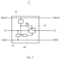
- FIG. 2 is a diagram of a structure of a circuit identification module 4 in a data cable according to an embodiment of this application.
- the data cable includes a type-A interface 1 and a type-C interface 2, where the type-A interface 1 and the type-C interface 2 are connected by using a cable 3, the type-A interface 1 and the type-C interface 2 each have a VBUS pin, a CC pin, a D+ pin, a D- pin, and a GND pin, and a VBUS pin, a D+ pin, a D- pin, and a GND pin of the type-A interface 1 are connected to a VBUS pin, a D+ pin, a D- pin, and a GND pin of the type-C interface 2, respectively;
- the comparator circuit 44 determines, based on a numerical relationship between the first voltage value and the second voltage value, whether there is signal transmission on the CC pin of the type-A interface 1.
- the first voltage value is a voltage value of an electrical signal obtained from the first input terminal
- the second voltage value is a voltage value of an electrical signal obtained from the second input terminal.
- the first terminal of the switch circuit 42 is controlled to be connected to the third terminal of the switch circuit 42 (that is, a CC cable is connected); when it is determined that there is no signal transmission on the CC pin, the first terminal of the switch circuit 42 is controlled to be connected to the second terminal of the switch circuit 42, that is, the CC cable is disconnected, and when the data cable is powered on, the CC pin of the type-C interface 2 obtains an electrical signal from the voltage regulator circuit 41 and the VBUS pin, so that a to-be-charged device can trigger non-PD charging when detecting the electrical signal by using the CC pin.
- the first terminal of the switch circuit 42 is connected to the second terminal of the switch circuit 42 indicates that the switch circuit 42 connects the output terminal of the voltage regulator circuit 41 to the CC pin of the type-C interface 2.
- the CC pin of the type-C interface 1 is disconnected from the CC pin of the type-A interface 1.
- the first terminal of the switch circuit 42 is connected to the third terminal of the switch circuit 42 indicates that the switch circuit 42 connects the CC pin of the type-A interface 1 to the CC pin of the type-C interface 2. In this case, the output terminal of the voltage regulator circuit 41 is disconnected from the CC pin of the type-C interface 2.
- the CC pin of the type-A interface 1 can be connected to the CC pin of the type-C interface 2 by using the CC cable.
- the VBUS pin, the D+ pin, the D- pin, and the GND pin in the type-A interface 1 are connected to the VBUS pin, the D+ pin, the D- pin, and the GND pin in the type-C interface 2 may be understood as follows:
- the VBUS pin in the type-A interface 1 is connected to the VBUS pin in the type-C interface 2 by using a VBUS cable
- the GND pin in the type-A interface 1 is connected to the GND pin in the type-C interface 2 by using a GND cable
- the D+ pin in the type- A interface 1 is connected to the D+ pin in the type-C interface 2 by using a D+ cable
- the D- pin in the type-A interface 1 is connected to the D- pin in the type-C interface 2 by using a D- cable.
- circuit identification module 4 disposed in the foregoing data cable may be disposed in the type-A interface 1, the type-C interface 2, or the cable 3 of the data cable. This is not specifically limited herein.
- PD charging may be understood as: transmitting a PD charging signal by using the CC cable, to perform PD charging negotiation with the to-be-charged device by using the PD charging signal, and charging the to-be-charged device according to a charging parameter determined in the PD charging negotiation.
- non-PD charging may be understood as: transmitting a communication signal by using the D+ pin and the D- pin, performing different charging negotiation with the charging device by using the communication signal, and charging the charging device according to a charging parameter determined in the charging negotiation.
- an electrical signal on the VBUS cable fluctuates within a specific range. If the VBUS cable is directly connected to the comparator circuit 44, a magnitude relationship between an electrical signal on the CC pin of the type-A interface 1 and an electrical signal on the VBUS cable is compared. When the electrical signal on the VBUS cable fluctuates, the comparator circuit 44 may obtain an incorrect result.
- the voltage regulator circuit 41 can obtain the electrical signal on the VBUS cable, and output an electrical signal with a constant voltage value, for example, an electrical signal with an output voltage value of 5 V (volt).
- a comparator compares an electrical signal output by the voltage regulator circuit 41 with an electrical signal output by the filtering circuit 43, to determine whether an electrical signal is transmitted on the CC cable, and when an electrical signal is transmitted on the CC cable, makes a CC communication channel conductive. However, when no electric signal is transmitted on the CC cable, the CC communication channel is disconnected, and the CC pin is pulled up to the VBUS cable, to trigger the to-be-charged device to perform non-PD charging.
- the voltage regulator circuit 41 is a low dropout regulator (low dropout regulator, LDO).
- LDO low dropout regulator
- the voltage regulator circuit 41 may be any voltage regulator that may adjust a fluctuating voltage to a stable voltage. This is not specifically limited herein.
- the filtering circuit 43 may be a shaping circuit.
- the filtering circuit 43 obtains a high-level signal from the CC cable, and correspondingly outputs a shaped high-level signal to the comparator circuit.
- the filtering circuit 43 releases an electrical signal, and outputs a shaped low-level signal to the comparator circuit when the released electrical signal is lower than a preset electrical signal.
- the electrical signal output by the voltage regulator circuit 41 may be between a low-level signal and a high-level signal, where the low-level signal is an electrical signal output by the filtering circuit 43 when no signal is transmitted on the CC cable, and the high-level signal is an electrical signal output by the filtering circuit 43 when a signal is transmitted on the CC cable.
- the switch circuit 42 includes two working states:
- the first terminal of the switch circuit 42 is connected to the second terminal of the switch circuit 42, that is, the switch circuit 42 connects the CC pin of the type-C interface 2 to the VBUS cable by using the voltage regulator circuit 41, and the CC pin of the type-C interface 2 is disconnected from the second terminal of the CC cable.
- the CC communication channel is disconnected, and the CC pin of the type-C interface 2 is pulled up to the VBUS cable.
- a structure of the data cable 2 is similar to a structure of a type-A to type-C data cable in the conventional technology, and a difference is that the CC pin of the type-C interface 2 in the type-A to type-C data cable in the conventional technology is connected to the VBUS cable by using a sixth resistor instead of the voltage regulator circuit 41.
- the data cable 2 in the foregoing working state has a same working principle as the type-A to type-C data cable in the conventional technology, that is, an electrical signal is transmitted to the to-be-charged device by using a CC pin connected to the VBUS cable, to instruct the to-be-charged device to perform non-PD charging.
- the first terminal of the switch circuit 42 is connected to the third terminal of the switch circuit 42, that is, the switch circuit 42 connects the CC pin of the type-C interface 2 to the CC cable, and the CC pin of the type-C interface 2 is disconnected from the VBUS cable. In this case, the CC communication channel is connected.
- the data cable 2 can perform PD charging negotiation with the to-be-charged device by using the CC cable and the CC pin that are connected.
- a mobile terminal such as a mobile phone usually supports quick charging of a DP communication protocol and a DM communication protocol.
- data minus (Data Minus, DM) charging communication and data positive (Data Positive, DP) charging communication protocols a communication signal is transmitted by using the D+ pin and the D- pin.
- An electronic device such as a notebook usually supports quick charging of the PD communication protocol.
- a communication signal is transmitted by using the CC pin.
- data cables that support the PD communication protocol all use a data cable in a type-C to type-C form
- data cables that support the DP/DM communication protocol all use a data cable in a type-A to type-C form. In this way, the data cable that supports the PD communication protocol and the data cable that supports the DP/DM communication protocol cannot be exchanged.
- the data cable in this implementation is a data cable that includes the type-A interface 1, and the CC pin is added to the type-A interface 1, and when a CC communication protocol signal is transmitted on the CC pin, the CC pin in the type-A interface 1 is connected to the CC pin in the type-A interface 2, so that PD quick charging can be performed on the to-be-charged device.
- the first terminal of the switch circuit 42 may be connected to the third terminal of the switch circuit 42, so that when the data cable is inserted into the to-be-charged device, PD charging communication is performed with the to-be-charged device by using the CC communication channel, and in a case that the CC communication signal is not obtained on the CC pin of the type-A interface within preset time after CC communication starts, the first terminal of the switch circuit 42 is switched to be connected to the second terminal of the switch circuit 42.
- the preset time may be 3 seconds, 5 seconds, or the like. This is not specifically limited herein.
- connection relationship between the VBUS pin, the D+ pin, the D- pin, and the GND pin in the type-A interface 1 and the type-C interface 2 and cables in the cable 3 is the same as a connection relationship between pins and cables in the conventional technology.
- the connection relationship between pins on the type-C interface and the type-A interface 1 and the cable 3 is specifically a connection relationship shown in the following Table 1: Table 1 Type-C interface Cable Type-A interface GND pin GND cable GND pin VBUS pin VBUS cable VBUS pin CC1 pin CC1 cable CC pin CC2 pin D+ pin D+ cable D+ pin D- pin D- cable D- pin
- the CC communication signal is adjusted to a stable analog signal by using the filtering circuit 43, and the analog signal is compared with a stable voltage output by the voltage regulator circuit 41 by using the comparator circuit 44, so that when there is a signal on the CC pin of the type-A interface 1, the comparator circuit 44 outputs a first control signal, and when there is no signal on the CC pin of the type-A interface 1, the comparator circuit 44 outputs a second control signal.
- the output first control signal and the output second control signal are more accurate, and an on/off state of the switch circuit 42 can be controlled more accurately according to the first control signal and the second control signal.
- the analog signal output by the filtering circuit may be a high-level signal.
- the comparator circuit 44 outputs the first control signal based on that the high-level signal is greater than the stable voltage output by the voltage regulator circuit 41, and the switch circuit 42 is connected to the first terminal and the third terminal of the switch circuit 42 in response to the first control signal.
- the analog signal output by the filtering circuit 43 may be a low-level signal.
- the comparator circuit 44 outputs the second control signal based on that the low-level signal is less than the stable voltage output by the voltage regulator circuit 41, and the switch circuit 42 is connected to the first terminal and the second terminal of the switch circuit 42 in response to the second control signal.
- the CC pin is disposed in the type-A interface 1, magnitude of the electrical signal output by the filtering circuit 43 and magnitude of the electrical signal output by the voltage regulator circuit 41 are compared by using the comparator circuit 44, and a corresponding control signal is output according to a comparison result, to control the CC pin to be connected or disconnected from the CC pin of the type-C interface 2, so that when there is a signal on the CC pin of the type-A interface 1, the CC pin is connected to the CC pin of the type-C interface 2, so that the PD communication channel in the data cable is connected, to support PD quick charging.
- the CC pin When there is no signal on the CC pin of the type-A interface 1, the CC pin is controlled to be disconnected from the CC pin of the type-C interface 2, so that the PD communication channel in the data cable is disconnected. In this case, PD quick charging is not supported, and the CC pin is connected to the VBUS by using the voltage regulator circuit 41, to instruct the to-be-charged device to perform non-PD charging. In this way, in a case that the to-be-charged device connected to the data cable supports PD quick charging, the PD communications channel in the data cable can be connected, and PD quick charging is performed on the to-be-charged device.
- the to-be-charged device connected to the data cable does not support PD quick charging
- the PD communication channel in the data cable is not connected, and a D+ cable is always connected to a D- cable, so that quick charging of DP/DM protocol communication is performed on the to-be-charged device.
- the circuit identification module 4 further includes a sixth resistor Rp.
- the sixth resistor Rp is connected between the switch circuit 4 and the CC pin of the type-C interface 2, and the switch circuit 42 is configured to connect the CC pin of the type-C interface 2 to the output terminal of the voltage regulator circuit 41 by using the sixth resistor Rp, or is configured to connect the CC pin of the type-C interface 2 to the CC pin of the type-A interface 1.
- resistance of the sixth resistor Rp may be 56 K ⁇ (kilohm).
- the voltage regulator circuit 41 can collect power from the VBUS cable and output a stable voltage to the sixth resistor Rp.
- the type-C interface 2 of the data cable is connected to a to-be-charged device that supports PD charging or is connected to a to-be-charged device that does not support PD charging, the CC pin of the type-C interface 2 has different electrical signal values.
- the to-be-charged device can be instructed, based on an electrical signal transmitted on the CC pin of the type-C interface 2, to perform PD charging communication or non-PD charging communication, where the non-PD charging communication is to transmit a charging negotiation signal by using the D+ pin and the D- pin.
- the resistance of the sixth resistor Rp may further be changed according to a stable output voltage of the voltage regulator circuit, and the resistance of the sixth resistor Rp is not specifically limited herein.
- the circuit identification module 4 is disposed in the cable 3, and a distance between the circuit identification module 4 and the type-A interface 1 is less than a distance between the circuit identification module 4 and the type-C interface 2.
- the circuit identification module 4 is disposed in the cable 3, to switch a corresponding connection relationship between the CC pin of the type- A interface 1 and the CC pin of the type-C interface 2 in the cable 3.
- a distance between the circuit identification module 4 and one end of the type-A interface 1 is less than a distance between the circuit identification module 4 and one end of the type-C interface 2, and the circuit identification module 4 may be disposed near the type-A interface 1.
- the circuit identification module 4 may alternatively be disposed near the type-C interface 2, and a problem that a circuit module of a relatively large diameter is disposed at a middle part of the cable 3 and affects fluency and beauty of the cable 3 can also be prevented.
- circuit identification module 4 may alternatively be disposed in the type-A interface 1 or the type-C interface 2, which does not affect a function of the circuit identification module 4. This is not specifically limited herein.
- the switch circuit 42 includes a first switching transistor Q3, a second switching transistor Q2, a first resistor R2, and a second resistor R3.
- a specific connection relationship between the first switching transistor Q3, the second switching transistor Q2, the first resistor R2, and the second resistor R3 is as follows:
- a first electrode of the first switching transistor Q3 and a first electrode of the second switching transistor Q2 are control terminals of the switch circuit 42, the first electrode of the first switching transistor Q3 and the first electrode of the second switching transistor Q2 are further connected to the GND pin by using the first resistor R2 and are connected to the output terminal of the comparator circuit 44 by using the second resistor R3, a second electrode of the first switching transistor Q3 is connected to the CC pin of the type-A interface 1, and a third electrode of the first switching transistor Q3 is connected to the CC pin of the type-C interface; and
- that the first switching transistor Q3 is in an on state indicates that the second electrode and the third electrode of the first switching transistor Q3 are conducted, and that the first switching transistor Q3 is in an off state indicates that the second electrode and the third electrode of the first switching transistor Q3 are disconnected.
- the second switching transistor Q2 is in an on state indicates that the second electrode and the third electrode of the second switching transistor Q2 are conducted, and that the second switching transistor Q2 is in an off state indicates that the second electrode and the third electrode of the second switching transistor Q2 are disconnected.
- the filtering circuit 43 adjusts the signal on the CC pin of the type-A interface 1 to a high-level signal, and the comparator circuit outputs the first control signal according to that the high-level signal is greater than the output voltage of the voltage regulator circuit 41.
- the first control signal may be a level signal of a first value, and an electrical signal of the first value is transmitted to the first electrode of the first switching transistor Q3 and the first electrode of the second switching transistor Q2 after voltage division by the first resistor R2 and the second resistor R3. In this case, the first switching transistor Q3 is on, and the second switching transistor Q2 is off.
- the filtering circuit 43 adjusts the signal on the CC pin of the type-A interface 1 to a low-level signal, and the comparator circuit outputs the second control signal according to that the low-level signal is less than the output voltage of the voltage regulator circuit 41.
- the second control signal may be a level signal of a second value, and an electrical signal of the second value is transmitted to the first electrode of the first switching transistor Q3 and the first electrode of the second switching transistor Q2 after voltage division by the first resistor R2 and the second resistor R3. In this case, the first switching transistor Q3 is off, and the second switching transistor Q2 is on.
- the first value is different from the second value. Specifically, in a case that the first switching transistor Q3 is an N-type switching transistor and the second switching transistor Q2 is a P-type switching transistor, the first value is greater than the second value; and in a case that the first switching transistor Q3 is a P-type switching transistor and the second switching transistor Q2 is an N-type switching transistor, the first value is less than the second value.
- the first switching transistor Q3 is an N-type metal oxide semiconductor (N-Metal-Oxide Semiconductor, NMOS) transistor
- the second switching transistor Q2 is a P-type metal oxide semiconductor (P-Metal-Oxide Semiconductor, PMOS) transistor.
- the first value is greater than the second value.
- the first electrode of the first switching transistor Q3 may be a gate, the second electrode may be a drain, and the third electrode may be a source; and the first electrode of the second switching transistor Q2 may be a gate, the second electrode may be a drain, and the third electrode may be a source.
- the first electrode of the first switching transistor Q3 receives a high-level signal, to conduct the second electrode and the third electrode of the first switching transistor Q3.
- the first electrode of the second switching transistor Q2 receives a high-level signal, to disconnect the second electrode and the third electrode of the second switching transistor Q2.
- the filtering circuit 43 does not output a high-level signal, that is, the filtering circuit 43 outputs a low-level signal
- the comparator circuit 44 outputs the second control signal according to the low-level signal.
- the second control signal may be a low-level signal.
- the first electrode of the first switching transistor Q3 receives the low-level signal, so that the first switching transistor Q3 is off, and the first electrode of the second switching transistor Q2 receives the low-level signal, so that the second switching transistor Q2 is on.
- the first switching transistor Q3 and the second switching transistor Q2 may alternatively be other types of transistors, and a connection circuit of each switching transistor in the switching circuit 42 is correspondingly changed, to connect or disconnect the CC pin of the type-A interface 1 and the CC pin of the type-A interface 2 according to a CC signal adjusted by the filtering circuit 43. This is not specifically limited herein.
- the switch circuit 42 in this implementation is an analog signal control circuit. In this way, a control unit may be prevented from being disposed in the circuit identification module 4, and an on/off state of the switch circuit 42 is controlled according to a digital control signal sent by the control unit, so that production costs of the switch circuit 42 can be reduced.
- the switch circuit 42 includes a switch, the first terminal of the switch circuit 42 is a fixed terminal of the switch, and both the second terminal and the third terminal of the switch circuit 42 are active terminals of the switch.
- the switch may be switched according to a control signal transmitted by the filtering circuit 43.
- the control signal may be a digital control signal.
- the comparator circuit 44 sends the first control signal to the switch, and the switch connects the fixed terminal to the third terminal in response to the first control signal, that is, connects the CC pin of the type-C interface 2 to the CC pin of the type-A interface 1.
- the comparator circuit 44 sends the second control signal to the switch, and the switch connects the fixed terminal to the second terminal in response to the second control signal, that is, connects the CC pin of the type-C interface 2 to the VBUS cable by using the sixth resistor Rp and the voltage regulator circuit 41.
- control unit may be further disposed in the switch circuit 42.
- the control unit is separately connected to the comparator circuit 44 and the switch, to convert the analog signal output by the comparator circuit 44 into a digital control signal, so as to control the on/off state of the switch by using the digital control signal.
- disposing the switch in the switch circuit can simplify a structure of the switch circuit.
- the filtering circuit 43 is an RC filtering circuit.
- the signal when there is a signal on the CC pin of the type-A interface 1, the signal may be a fluctuating level signal, and the fluctuating level signal may be adjusted to a relatively stable level signal by using the RC filtering circuit, and is input to the comparator circuit 44, so that the comparator circuit 44 outputs a more accurate and stable control signal.
- control signal output by the comparator circuit 44 can be more stable and reliable.
- the filtering circuit 43 includes a third resistor R1 and a capacitor C1.
- a first terminal of the third resistor R1 is connected to the CC pin of the type-A interface 1
- a second terminal of the third resistor R1 is connected to a first terminal of the capacitor C1
- a second terminal of the capacitor C1 is connected to the GND pin of the type-C interface 2
- a first terminal of the capacitor C1 is further connected to the second input terminal of the comparator circuit 44.
- the filtering circuit 43 when there is no signal on the CC pin of the type-A interface 1, the filtering circuit 43 outputs a low-level signal (which may be a level signal whose value is 0).
- a low-level signal which may be a level signal whose value is 0.
- the capacitor C1 When there is a fluctuating level signal on the CC pin of the type-A interface 1, the capacitor C1 is charged when the level signal rises, and the capacitor C1 is discharged when the level signal decreases, so that the filtering circuit 43 outputs a steady high-level signal (a level signal whose value is greater than 0), and the high-level signal is input to the comparator circuit 44 for comparison with the electrical signal output by the voltage regulator circuit 41, so that the comparator circuit 44 outputs an accurate control signal to control the on/off state of the switch circuit 42.
- the comparator circuit 44 may be used to compare a level signal output by the filtering circuit 43, and output an accurate control signal.
- the level signal output by the filtering circuit 43 is a solution in which a level value fluctuates in a value range.
- a control signal with an accurate value that is output by the comparator circuit 44 controls the on/off state of the switch circuit 42, so that control sensitivity of the switch circuit 42 can be improved.
- capacitance of the capacitor C1 is greater than preset capacitance.
- the preset capacitance may be determined according to identification precision of the comparator circuit 44, a level value of the signal on the CC pin of the type-A interface 1, a change characteristic, and the like. This is not specifically limited herein.
- the capacitance of the capacitor C1 is greater than the preset capacitance, so that when a level value of a signal transmitted on the CC pin of the type-A interface 1 fluctuates, the capacitor C1 is charged when a level of the transmission signal rises, and after charging, the capacitor C1 is discharged when the level value of the signal transmitted on the CC pin of the type-A interface 1 decreases. In this way, in a period in which a fluctuating electrical signal is transmitted on the CC pin of the type-A interface 1, a value of an electrical signal transmitted by the filtering circuit 43 to the comparator circuit 44 is relatively stable.
- the comparator circuit 44 includes a fourth resistor R4, a fifth resistor R5, and a comparator U1.
- a first terminal of the comparator U1 is connected to the control terminal of the switch circuit 42, a second terminal of the comparator U1 is connected to the output terminal of the voltage regulator circuit 41, a third terminal of the comparator U1 is connected to the output terminal of the filtering circuit 43, a fourth terminal of the comparator U1 is connected to the GND pin, a fifth terminal of the comparator U1 is connected to a first terminal of the fourth resistor R4 and a first terminal of the fifth resistor R5, a second terminal of the fourth resistor R4 is connected to the GND pin, and a second terminal of the fifth resistor R5 is connected to the second terminal of the comparator U1.
- the third terminal of the comparator U1 is the second input terminal of the comparator circuit 44, and the second terminal of the fifth resistor R5 and the second terminal of the comparator U1 are the same as the first input terminal of the comparator circuit 44.
- the output terminal of the filtering circuit 43 In operation, in a case that there is a signal on the CC pin of the type-A interface 1, the output terminal of the filtering circuit 43 outputs a high-level signal, an electrical signal value on the third terminal of the comparator U1 is greater than an electrical signal value on the fifth terminal of the comparator U1, the comparator U1 outputs a first control signal, and the switch circuit 42 connects the first terminal to the third terminal of the switch circuit 42 in response to the first control signal; and in a case that there is no signal on the CC pin of the type-A interface 1, the output terminal of the filtering circuit 43 outputs a low-level signal, an electrical signal value on the third terminal of the comparator U1 is less than or equal to an electrical signal value on the fifth terminal of the comparator U1, the comparator U1 outputs a second control signal, and the switch circuit 42 connects the first terminal to the second terminal of the switch circuit 42 in response to the second control signal.
- the fourth resistor R4 and the fifth resistor R5 are configured to divide the electric signal output by the voltage regulator circuit 41, so that an electric signal value obtained by the fifth terminal of the comparator U1 from the voltage regulator circuit 41 meets the following conditions:
- the fourth resistor R4 and the fifth resistor R5 form a proportional circuit, to adjust a voltage value obtained by the fifth terminal of the comparator U1, so as to output control signals of different level values to the switch circuit 42 in a case that there is a signal or no signal on the CC pin of the type-A interface 1, thereby controlling the on/off state of the switch circuit 42.
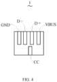
- the GND pin, the D+ pin, the D- pin, and the VBUS pin are disposed on a first side of the type-A interface 1
- the CC pin is disposed on a second side of the type-A interface 1
- the first side and the second side of the type-A interface 1 are two opposite sides.
- the CC pin is disposed on the second side of the type-A interface 1, so that a structure and location distribution of the GND pin, the D+ pin, the D- pin, and the VBUS pin on the first side of the Type-A interface 1 are the same as those of a type-A interface in the conventional technology.
- the data cable provided in this embodiment of this application can be connected to a charger with a conventional type-A interface.
- the charging device only supports quick charging of the DP/DM communication protocol.
- An embodiment of this application further provides a charging device, and the charging device includes a charger and the data cable provided in the foregoing embodiments.
- the charger includes a PD charging processing module, and when the charger is connected to the data cable, the PD charging processing module is connected to the CC pin of the type-A interface.
- the charger includes a type-A female connector that matches the type-A interface in the data cable, and the type-A female connector includes a VBUS pin, a CC pin, a D+ pin, a D- pin, and a GND pin.
- the type-A female connector that matches the type-A interface in the data cable may be understood as follows: In a case that the type-A interface in the data cable 2 is inserted into the type-A female connector in the charger 1, the type-A interface is connected to a same pin in the type-A female connector.
- the charger may further include a D+/D- charging module (which may also be referred to as a non-PD charging processing module).
- a charging signal of the D+/D- charging module is transmitted by using a D+ pin and a D- pin.
- the PD charging module is connected to the CC pin to perform communication of a PD protocol with a to-be-charged device by using the CC pin, to support PD quick charging.
- the D+/D- charging module is connected to the D+ pin and the D- pin to perform communication of a DP/DM protocol with the to-be-charged device by using the D+ pin and the D- pin, to support DP/DM quick charging.
- the type-A female connector that matches the type-A interface may further be connected to a type-A interface on a conventional data cable, and in a case that the type-A female connector of the charger is connected to the type-A interface on the conventional data cable, only charging of the DP/DM protocol is supported.
- the charging device provided in this embodiment of this application has the type-A interface, supports charging of the PD protocol and charging of the DP/DM protocol, and has a same beneficial effect as that of the data cable provided in this embodiment of this application. Details are not described herein again.
- the foregoing method embodiments may be implemented by using software and a required universal hardware platform, or certainly may be implemented by using hardware. However, in many cases, the former is a better implementation.
- the technical solutions of this application essentially or the part contributing to existing technologies may be implemented in a form of a software product.
- the computer software product is stored in a storage medium (such as a ROM/RAM, a magnetic disk, or an optical disc) and includes several instructions for instructing a terminal (which may be a mobile phone, a computer, a server, an air conditioner, or a network device) to execute the methods described in the embodiments of this application.
Landscapes
- Engineering & Computer Science (AREA)
- Theoretical Computer Science (AREA)
- Physics & Mathematics (AREA)
- General Physics & Mathematics (AREA)
- General Engineering & Computer Science (AREA)
- Power Engineering (AREA)
- Microelectronics & Electronic Packaging (AREA)
- Electromagnetism (AREA)
- Radar, Positioning & Navigation (AREA)
- Automation & Control Theory (AREA)
- Computer Hardware Design (AREA)
- Power Sources (AREA)
- Charge And Discharge Circuits For Batteries Or The Like (AREA)
- Dc Digital Transmission (AREA)
- Data Exchanges In Wide-Area Networks (AREA)
- Devices For Supply Of Signal Current (AREA)
Description
- This application pertains to the field of communication technologies, and specifically relates to a data cable and a charging device.
- With the development of science and technology, quick charging is increasingly widely used.
- In a related technology, a power delivery (Power Delivery, PD) protocol is generally used for quick charging. A charger that supports charging of the PD protocol needs to use a configuration channel (Configuration Channel, CC) signal cable for communication. The charger that supports charging of the PD protocol generally uses a type-C (Type-C) interface and has a Type-C to Type-C data cable. A data cable that uses a type-A (Type-A or Standard-A) interface performs communication by using a D+/D-signal cable, and cannot support charging in the PD protocol. Therefore, a type-A interface on the data cable does not support charging in the PD protocol.
- One mentions here, the document
CN108233130B considered Closest Prior Art. One identifies as well the Article 54(3) EPC documentEP4160856A1 . - Embodiments of this application are to provide a data cable and a charging device, which can resolve a problem that a data cable with a type-A interface does not support charging in a PD protocol.
- To resolve the foregoing technical problem, this application is implemented as follows:
- According to a first aspect, an embodiment of this application provides a data cable, including: a type-A interface and a type-C interface, where the type-A interface and the type-C interface are connected by using a cable, the type-A interface and the type-C interface each have a VBUS pin, a CC pin, a D+ pin, a D- pin, and a GND pin, and a VBUS pin, a D+ pin, a D- pin, and a GND pin of the type-A interface are connected to a VBUS pin, a D+ pin, a D- pin, and a GND pin of the type-C interface, respectively;
- a circuit identification module is disposed in the data cable, and the circuit identification module includes a switch circuit, a filtering circuit, a voltage regulator circuit, and a comparator circuit; and
- the switch circuit is connected to the CC pin of the type-C interface, an output terminal of the voltage regulator circuit, and the CC pin of the type-A interface, a control terminal of the switch circuit is connected to an output terminal of the comparator circuit, an input terminal of the voltage regulator circuit is connected to a VBUS cable in the cable, an output terminal of the voltage regulator circuit is further connected to a first input terminal of the comparator circuit, a second input terminal of the comparator circuit is connected to an output terminal of the filtering circuit, and an input terminal of the filtering circuit is connected to the CC pin of the type-A interface; where
- under the control of the comparator circuit, the switch circuit connects the CC pin of the type-A interface to the CC pin of the type-C interface, or connects the output terminal of the voltage regulator circuit to the CC pin of the type-C interface.
- According to a second aspect, an embodiment of this application provides a charging device, including a data cable and a charger. The data cable is the data cable in the first aspect, the charger includes a PD charging processing module, and when the charger is connected to the data cable, the PD charging processing module is connected to the CC pin in the type-A interface.
- In the embodiments of this application, a CC pin is disposed in a type-A interface of a data cable, a CC communication signal transmitted on the CC pin of the type-A interface is filtered into a stable control signal by using a filtering circuit, and a comparator circuit is used to compare the analog signal with a stable voltage provided by a voltage regulator circuit, to output a corresponding control signal, so that when there is a signal on the CC pin of the type-A interface and when there is no signal on the CC pin of the type-A interface, control signals output by the comparator circuit are different control signals; an on/off state of a switch circuit is controlled according to the control signal, so that when the switch circuit connects an output terminal of the voltage regulator circuit to a CC pin of a type-C interface, the data cable can only perform non-PD protocol communication by using a D+ pin and a D- pin; and when the switch circuit connects the CC pin of the type-A interface to the CC pin of the type-C interface, the data cable can support non-PD protocol communication by using the D+ pin and the D- pin, and can also support PD protocol communication by using the CC pin. In this way, a data cable with the type-A interface can support charging in a PD protocol.
-
-
FIG. 1 is a diagram of a structure of a data cable according to an embodiment of this application; -
FIG. 2 is a diagram of a structure of a circuit identification module in a data cable according to an embodiment of this application; -
FIG. 3 is a circuit diagram of a circuit identification module in a data cable according to an embodiment of this application; and -
FIG. 4 is a diagram of a structure of a type-A interface in a data cable according to an embodiment of this application. - The following clearly and completely describes the technical solutions in the embodiments of this application with reference to the accompanying drawings in the embodiments of this application. Apparently, the described embodiments are some rather than all of the embodiments of this application. However, the invention is defined by the features of the independent claims. Preferred embodiments are defined in the dependent claims.
- Terms "first" and "second" in the specification and claims of this application are used to distinguish between similar objects, and do not need to be used to describe a specific order or sequence. It should be understood that data used in this way may be interchangeable in an appropriate case, so that the embodiments of this application can be implemented in a sequence other than those shown or described herein, and objects distinguished by "first" and "second" are generally of a same type, and a quantity of objects is not limited. For example, there may be one or more first targets. In addition, in the specification and the claims, "and/or" represents at least one of connected objects, and the character "/" generally represents an "or" relationship between associated objects.
- With reference to the accompanying drawings, a data cable and a charging device provided in the embodiments of this application are described in detail below by using a specific embodiment and an application scenario thereof.
- Refer to both
FIG. 1 andFIG. 2 .FIG. 1 shows a structure of a data cable according to an embodiment of this application. -
FIG. 2 is a diagram of a structure of acircuit identification module 4 in a data cable according to an embodiment of this application. - The data cable includes a type-
A interface 1 and a type-C interface 2, where the type-A interface 1 and the type-C interface 2 are connected by using acable 3, the type-A interface 1 and the type-C interface 2 each have a VBUS pin, a CC pin, a D+ pin, a D- pin, and a GND pin, and a VBUS pin, a D+ pin, a D- pin, and a GND pin of the type-A interface 1 are connected to a VBUS pin, a D+ pin, a D- pin, and a GND pin of the type-C interface 2, respectively; - a
circuit identification module 4 is disposed in the data cable, and thecircuit identification module 4 includes aswitch circuit 42, afiltering circuit 43, avoltage regulator circuit 41, and acomparator circuit 44; and - a specific connection relationship of the
switch circuit 42, thefiltering circuit 43, thevoltage regulator circuit 41, and thecomparator circuit 44 is as follows: a first terminal of theswitch circuit 42 is connected to the CC pin of the type-C interface 2, a second terminal of theswitch circuit 42 is connected to an output terminal of thevoltage regulator circuit 41, a third terminal of theswitch circuit 42 is connected to the CC pin of the type-A interface 1, a control terminal of theswitch circuit 42 is connected to an output terminal of thecomparator circuit 44, an input terminal of thevoltage regulator circuit 41 is connected to a VBUS cable in thecable 3, an output terminal of thevoltage regulator circuit 41 is further connected to a first terminal of thecomparator circuit 44, a second terminal of thecomparator circuit 44 is connected to an output terminal of thefiltering circuit 43, and an input terminal of thefiltering circuit 43 is connected to the CC cable; and - under the control of the
comparator circuit 44, the first terminal of theswitch circuit 42 is connected to the second terminal or the third terminal of theswitch circuit 42. - In operation, the
comparator circuit 44 determines, based on a numerical relationship between the first voltage value and the second voltage value, whether there is signal transmission on the CC pin of the type-A interface 1. The first voltage value is a voltage value of an electrical signal obtained from the first input terminal, and the second voltage value is a voltage value of an electrical signal obtained from the second input terminal. - In addition, when it is determined that there is signal transmission on the CC pin, the first terminal of the
switch circuit 42 is controlled to be connected to the third terminal of the switch circuit 42 (that is, a CC cable is connected); when it is determined that there is no signal transmission on the CC pin, the first terminal of theswitch circuit 42 is controlled to be connected to the second terminal of theswitch circuit 42, that is, the CC cable is disconnected, and when the data cable is powered on, the CC pin of the type-C interface 2 obtains an electrical signal from thevoltage regulator circuit 41 and the VBUS pin, so that a to-be-charged device can trigger non-PD charging when detecting the electrical signal by using the CC pin. - Specifically, that the first terminal of the
switch circuit 42 is connected to the second terminal of theswitch circuit 42 indicates that theswitch circuit 42 connects the output terminal of thevoltage regulator circuit 41 to the CC pin of the type-C interface 2. In this case, the CC pin of the type-C interface 1 is disconnected from the CC pin of the type-A interface 1. - In addition, that the first terminal of the
switch circuit 42 is connected to the third terminal of theswitch circuit 42 indicates that theswitch circuit 42 connects the CC pin of the type-A interface 1 to the CC pin of the type-C interface 2. In this case, the output terminal of thevoltage regulator circuit 41 is disconnected from the CC pin of the type-C interface 2. - In addition, the CC pin of the type-
A interface 1 can be connected to the CC pin of the type-C interface 2 by using the CC cable. - In addition, that the VBUS pin, the D+ pin, the D- pin, and the GND pin in the type-
A interface 1 are connected to the VBUS pin, the D+ pin, the D- pin, and the GND pin in the type-C interface 2 may be understood as follows: The VBUS pin in the type-A interface 1 is connected to the VBUS pin in the type-C interface 2 by using a VBUS cable, the GND pin in the type-A interface 1 is connected to the GND pin in the type-C interface 2 by using a GND cable, the D+ pin in the type-A interface 1 is connected to the D+ pin in the type-C interface 2 by using a D+ cable, and the D- pin in the type-A interface 1 is connected to the D- pin in the type-C interface 2 by using a D- cable. - In addition, the
circuit identification module 4 disposed in the foregoing data cable may be disposed in the type-A interface 1, the type-C interface 2, or thecable 3 of the data cable. This is not specifically limited herein. - In specific implementation, PD charging may be understood as: transmitting a PD charging signal by using the CC cable, to perform PD charging negotiation with the to-be-charged device by using the PD charging signal, and charging the to-be-charged device according to a charging parameter determined in the PD charging negotiation.
- In addition, the foregoing non-PD charging may be understood as: transmitting a communication signal by using the D+ pin and the D- pin, performing different charging negotiation with the charging device by using the communication signal, and charging the charging device according to a charging parameter determined in the charging negotiation.
- In addition, in a conventional technology, an electrical signal on the VBUS cable fluctuates within a specific range. If the VBUS cable is directly connected to the
comparator circuit 44, a magnitude relationship between an electrical signal on the CC pin of the type-A interface 1 and an electrical signal on the VBUS cable is compared. When the electrical signal on the VBUS cable fluctuates, thecomparator circuit 44 may obtain an incorrect result. - In this implementation, the
voltage regulator circuit 41 can obtain the electrical signal on the VBUS cable, and output an electrical signal with a constant voltage value, for example, an electrical signal with an output voltage value of 5 V (volt). In this way, a comparator compares an electrical signal output by thevoltage regulator circuit 41 with an electrical signal output by thefiltering circuit 43, to determine whether an electrical signal is transmitted on the CC cable, and when an electrical signal is transmitted on the CC cable, makes a CC communication channel conductive. However, when no electric signal is transmitted on the CC cable, the CC communication channel is disconnected, and the CC pin is pulled up to the VBUS cable, to trigger the to-be-charged device to perform non-PD charging. - For example, the
voltage regulator circuit 41 is a low dropout regulator (low dropout regulator, LDO). - Certainly, the
voltage regulator circuit 41 may be any voltage regulator that may adjust a fluctuating voltage to a stable voltage. This is not specifically limited herein. - In specific implementation, the
filtering circuit 43 may be a shaping circuit. When a signal is transmitted on the CC cable, thefiltering circuit 43 obtains a high-level signal from the CC cable, and correspondingly outputs a shaped high-level signal to the comparator circuit. When no signal is transmitted on the CC cable, thefiltering circuit 43 releases an electrical signal, and outputs a shaped low-level signal to the comparator circuit when the released electrical signal is lower than a preset electrical signal. - Specifically, the electrical signal output by the
voltage regulator circuit 41 may be between a low-level signal and a high-level signal, where the low-level signal is an electrical signal output by thefiltering circuit 43 when no signal is transmitted on the CC cable, and the high-level signal is an electrical signal output by thefiltering circuit 43 when a signal is transmitted on the CC cable. - In specific working, the
switch circuit 42 includes two working states: - In a first working state, the first terminal of the
switch circuit 42 is connected to the second terminal of theswitch circuit 42, that is, theswitch circuit 42 connects the CC pin of the type-C interface 2 to the VBUS cable by using thevoltage regulator circuit 41, and the CC pin of the type-C interface 2 is disconnected from the second terminal of the CC cable. In this case, the CC communication channel is disconnected, and the CC pin of the type-C interface 2 is pulled up to the VBUS cable. - In this case, a structure of the
data cable 2 is similar to a structure of a type-A to type-C data cable in the conventional technology, and a difference is that the CC pin of the type-C interface 2 in the type-A to type-C data cable in the conventional technology is connected to the VBUS cable by using a sixth resistor instead of thevoltage regulator circuit 41. - In application, the
data cable 2 in the foregoing working state has a same working principle as the type-A to type-C data cable in the conventional technology, that is, an electrical signal is transmitted to the to-be-charged device by using a CC pin connected to the VBUS cable, to instruct the to-be-charged device to perform non-PD charging. - In a second working state, the first terminal of the
switch circuit 42 is connected to the third terminal of theswitch circuit 42, that is, theswitch circuit 42 connects the CC pin of the type-C interface 2 to the CC cable, and the CC pin of the type-C interface 2 is disconnected from the VBUS cable. In this case, the CC communication channel is connected. - In this case, the
data cable 2 can perform PD charging negotiation with the to-be-charged device by using the CC cable and the CC pin that are connected. - In the conventional technology, a mobile terminal such as a mobile phone usually supports quick charging of a DP communication protocol and a DM communication protocol. In data minus (Data Minus, DM) charging communication and data positive (Data Positive, DP) charging communication protocols, a communication signal is transmitted by using the D+ pin and the D- pin. An electronic device such as a notebook usually supports quick charging of the PD communication protocol. In the PD communication protocol, a communication signal is transmitted by using the CC pin. In addition, in the conventional technology, data cables that support the PD communication protocol all use a data cable in a type-C to type-C form, and data cables that support the DP/DM communication protocol all use a data cable in a type-A to type-C form. In this way, the data cable that supports the PD communication protocol and the data cable that supports the DP/DM communication protocol cannot be exchanged.
- However, the data cable in this implementation is a data cable that includes the type-
A interface 1, and the CC pin is added to the type-A interface 1, and when a CC communication protocol signal is transmitted on the CC pin, the CC pin in the type-A interface 1 is connected to the CC pin in the type-A interface 2, so that PD quick charging can be performed on the to-be-charged device. - In addition, in actual application, in a case that the to-be-charged device supports only non-PD quick charging of the DP and DM communication protocols, DP and DM communication channels on the data cable are still in an on state, so that quick charging of the DP and DM protocols can be provided for the to-be-charged device.
- In addition, during operation, in an initial state in which the data cable provided in this embodiment of this application is not connected to a power supply, the first terminal of the
switch circuit 42 may be connected to the third terminal of theswitch circuit 42, so that when the data cable is inserted into the to-be-charged device, PD charging communication is performed with the to-be-charged device by using the CC communication channel, and in a case that the CC communication signal is not obtained on the CC pin of the type-A interface within preset time after CC communication starts, the first terminal of theswitch circuit 42 is switched to be connected to the second terminal of theswitch circuit 42. The preset time may be 3 seconds, 5 seconds, or the like. This is not specifically limited herein. - In addition, a connection relationship between the VBUS pin, the D+ pin, the D- pin, and the GND pin in the type-
A interface 1 and the type-C interface 2 and cables in thecable 3 is the same as a connection relationship between pins and cables in the conventional technology. For example, the connection relationship between pins on the type-C interface and the type-A interface 1 and thecable 3 is specifically a connection relationship shown in the following Table 1:Table 1 Type-C interface Cable Type-A interface GND pin GND cable GND pin VBUS pin VBUS cable VBUS pin CC1 pin CC1 cable CC pin CC2 pin D+ pin D+ cable D+ pin D- pin D- cable D- pin - In implementation, in a case that the CC communication signal is received on the CC pin of the type-
A interface 1, the CC communication signal is adjusted to a stable analog signal by using thefiltering circuit 43, and the analog signal is compared with a stable voltage output by thevoltage regulator circuit 41 by using thecomparator circuit 44, so that when there is a signal on the CC pin of the type-A interface 1, thecomparator circuit 44 outputs a first control signal, and when there is no signal on the CC pin of the type-A interface 1, thecomparator circuit 44 outputs a second control signal. In this way, the output first control signal and the output second control signal are more accurate, and an on/off state of theswitch circuit 42 can be controlled more accurately according to the first control signal and the second control signal. - Specifically, in a case that there is a signal on the CC pin of the type-
A interface 1, the analog signal output by the filtering circuit may be a high-level signal. In this way, thecomparator circuit 44 outputs the first control signal based on that the high-level signal is greater than the stable voltage output by thevoltage regulator circuit 41, and theswitch circuit 42 is connected to the first terminal and the third terminal of theswitch circuit 42 in response to the first control signal. In a case that there is no signal on the CC pin of the type-A interface 1, the analog signal output by thefiltering circuit 43 may be a low-level signal. In this way, thecomparator circuit 44 outputs the second control signal based on that the low-level signal is less than the stable voltage output by thevoltage regulator circuit 41, and theswitch circuit 42 is connected to the first terminal and the second terminal of theswitch circuit 42 in response to the second control signal. - In this implementation, the CC pin is disposed in the type-
A interface 1, magnitude of the electrical signal output by thefiltering circuit 43 and magnitude of the electrical signal output by thevoltage regulator circuit 41 are compared by using thecomparator circuit 44, and a corresponding control signal is output according to a comparison result, to control the CC pin to be connected or disconnected from the CC pin of the type-C interface 2, so that when there is a signal on the CC pin of the type-A interface 1, the CC pin is connected to the CC pin of the type-C interface 2, so that the PD communication channel in the data cable is connected, to support PD quick charging. When there is no signal on the CC pin of the type-A interface 1, the CC pin is controlled to be disconnected from the CC pin of the type-C interface 2, so that the PD communication channel in the data cable is disconnected. In this case, PD quick charging is not supported, and the CC pin is connected to the VBUS by using thevoltage regulator circuit 41, to instruct the to-be-charged device to perform non-PD charging. In this way, in a case that the to-be-charged device connected to the data cable supports PD quick charging, the PD communications channel in the data cable can be connected, and PD quick charging is performed on the to-be-charged device. In a case that the to-be-charged device connected to the data cable does not support PD quick charging, the PD communication channel in the data cable is not connected, and a D+ cable is always connected to a D- cable, so that quick charging of DP/DM protocol communication is performed on the to-be-charged device. - In an optional implementation, the
circuit identification module 4 further includes a sixth resistor Rp. The sixth resistor Rp is connected between theswitch circuit 4 and the CC pin of the type-C interface 2, and theswitch circuit 42 is configured to connect the CC pin of the type-C interface 2 to the output terminal of thevoltage regulator circuit 41 by using the sixth resistor Rp, or is configured to connect the CC pin of the type-C interface 2 to the CC pin of the type-A interface 1. - In specific implementation, resistance of the sixth resistor Rp may be 56 KΩ (kilohm). When the CC pin of the type-
C interface 2 is connected to the output terminal of thevoltage regulator circuit 41 by using the sixth resistor Rp, thevoltage regulator circuit 41 can collect power from the VBUS cable and output a stable voltage to the sixth resistor Rp. When the type-C interface 2 of the data cable is connected to a to-be-charged device that supports PD charging or is connected to a to-be-charged device that does not support PD charging, the CC pin of the type-C interface 2 has different electrical signal values. Therefore, the to-be-charged device can be instructed, based on an electrical signal transmitted on the CC pin of the type-C interface 2, to perform PD charging communication or non-PD charging communication, where the non-PD charging communication is to transmit a charging negotiation signal by using the D+ pin and the D- pin. - It should be noted that in specific implementation, the resistance of the sixth resistor Rp may further be changed according to a stable output voltage of the voltage regulator circuit, and the resistance of the sixth resistor Rp is not specifically limited herein.
- In an optional implementation, the
circuit identification module 4 is disposed in thecable 3, and a distance between thecircuit identification module 4 and the type-A interface 1 is less than a distance between thecircuit identification module 4 and the type-C interface 2. - In this implementation, the
circuit identification module 4 is disposed in thecable 3, to switch a corresponding connection relationship between the CC pin of the type-A interface 1 and the CC pin of the type-C interface 2 in thecable 3. - In addition, a distance between the
circuit identification module 4 and one end of the type-A interface 1 is less than a distance between thecircuit identification module 4 and one end of the type-C interface 2, and thecircuit identification module 4 may be disposed near the type-A interface 1. In this way, a problem that a circuit board structure including thecircuit identification module 4 is disposed at a middle part of thecable 3 and affects fluency and beauty of thecable 3 can be prevented. Certainly, in specific implementation, thecircuit identification module 4 may alternatively be disposed near the type-C interface 2, and a problem that a circuit module of a relatively large diameter is disposed at a middle part of thecable 3 and affects fluency and beauty of thecable 3 can also be prevented. - It should be noted that, in specific implementation, the
circuit identification module 4 may alternatively be disposed in the type-A interface 1 or the type-C interface 2, which does not affect a function of thecircuit identification module 4. This is not specifically limited herein. - In an optional implementation, as shown in
FIG. 3 , theswitch circuit 42 includes a first switching transistor Q3, a second switching transistor Q2, a first resistor R2, and a second resistor R3. - A specific connection relationship between the first switching transistor Q3, the second switching transistor Q2, the first resistor R2, and the second resistor R3 is as follows:
- A first electrode of the first switching transistor Q3 and a first electrode of the second switching transistor Q2 are control terminals of the
switch circuit 42, the first electrode of the first switching transistor Q3 and the first electrode of the second switching transistor Q2 are further connected to the GND pin by using the first resistor R2 and are connected to the output terminal of thecomparator circuit 44 by using the second resistor R3, a second electrode of the first switching transistor Q3 is connected to the CC pin of the type-A interface 1, and a third electrode of the first switching transistor Q3 is connected to the CC pin of the type-C interface; and - a second electrode of the second switching transistor Q2 is connected to the output terminal of the
voltage regulator circuit 41, and a third electrode of the second switching transistor Q2 is connected to the CC pin of the type-C interface 2; where - in a case that there is no signal on the CC pin of the type-
A interface 1, the first switching transistor Q3 is in an off state, and the second switching transistor Q2 is in an on state; and in a case that there is a signal on the CC pin of the type-A interface 1, the first switching transistor Q3 is in an on state, and the second switching transistor Q2 is in an off state. - In specific implementation, that the first switching transistor Q3 is in an on state indicates that the second electrode and the third electrode of the first switching transistor Q3 are conducted, and that the first switching transistor Q3 is in an off state indicates that the second electrode and the third electrode of the first switching transistor Q3 are disconnected.
- Similarly, that the second switching transistor Q2 is in an on state indicates that the second electrode and the third electrode of the second switching transistor Q2 are conducted, and that the second switching transistor Q2 is in an off state indicates that the second electrode and the third electrode of the second switching transistor Q2 are disconnected.
- That the first electrode of the first switching transistor Q3 and the first electrode of the second switching transistor Q2 are control terminals of the
switch circuit 42 indicates that the first electrode of the first switching transistor Q3 and the first electrode of the second switching transistor Q2 are separately connected to the output terminal of thecomparator circuit 44. - In specific implementation, in a case that a signal is transmitted on the CC pin of the type-
A interface 1, thefiltering circuit 43 adjusts the signal on the CC pin of the type-A interface 1 to a high-level signal, and the comparator circuit outputs the first control signal according to that the high-level signal is greater than the output voltage of thevoltage regulator circuit 41. The first control signal may be a level signal of a first value, and an electrical signal of the first value is transmitted to the first electrode of the first switching transistor Q3 and the first electrode of the second switching transistor Q2 after voltage division by the first resistor R2 and the second resistor R3. In this case, the first switching transistor Q3 is on, and the second switching transistor Q2 is off. - In addition, in a case that no signal is transmitted on the CC pin of the type-
A interface 1, thefiltering circuit 43 adjusts the signal on the CC pin of the type-A interface 1 to a low-level signal, and the comparator circuit outputs the second control signal according to that the low-level signal is less than the output voltage of thevoltage regulator circuit 41. The second control signal may be a level signal of a second value, and an electrical signal of the second value is transmitted to the first electrode of the first switching transistor Q3 and the first electrode of the second switching transistor Q2 after voltage division by the first resistor R2 and the second resistor R3. In this case, the first switching transistor Q3 is off, and the second switching transistor Q2 is on. - The first value is different from the second value. Specifically, in a case that the first switching transistor Q3 is an N-type switching transistor and the second switching transistor Q2 is a P-type switching transistor, the first value is greater than the second value; and in a case that the first switching transistor Q3 is a P-type switching transistor and the second switching transistor Q2 is an N-type switching transistor, the first value is less than the second value.
- In an implementation, the first switching transistor Q3 is an N-type metal oxide semiconductor (N-Metal-Oxide Semiconductor, NMOS) transistor, and the second switching transistor Q2 is a P-type metal oxide semiconductor (P-Metal-Oxide Semiconductor, PMOS) transistor.
- In this case, the first value is greater than the second value.
- In application, the first electrode of the first switching transistor Q3 may be a gate, the second electrode may be a drain, and the third electrode may be a source; and the first electrode of the second switching transistor Q2 may be a gate, the second electrode may be a drain, and the third electrode may be a source. In this way, when there is a signal on the CC pin of the type-
A interface 1, the first electrode of the first switching transistor Q3 receives a high-level signal, to conduct the second electrode and the third electrode of the first switching transistor Q3. In this case, the first electrode of the second switching transistor Q2 receives a high-level signal, to disconnect the second electrode and the third electrode of the second switching transistor Q2. - Correspondingly, in a case that there is no signal on the CC pin of the type-
A interface 1, thefiltering circuit 43 does not output a high-level signal, that is, thefiltering circuit 43 outputs a low-level signal, and thecomparator circuit 44 outputs the second control signal according to the low-level signal. The second control signal may be a low-level signal. The first electrode of the first switching transistor Q3 receives the low-level signal, so that the first switching transistor Q3 is off, and the first electrode of the second switching transistor Q2 receives the low-level signal, so that the second switching transistor Q2 is on. - Certainly, in specific implementation, the first switching transistor Q3 and the second switching transistor Q2 may alternatively be other types of transistors, and a connection circuit of each switching transistor in the switching
circuit 42 is correspondingly changed, to connect or disconnect the CC pin of the type-A interface 1 and the CC pin of the type-A interface 2 according to a CC signal adjusted by thefiltering circuit 43. This is not specifically limited herein. - The
switch circuit 42 in this implementation is an analog signal control circuit. In this way, a control unit may be prevented from being disposed in thecircuit identification module 4, and an on/off state of theswitch circuit 42 is controlled according to a digital control signal sent by the control unit, so that production costs of theswitch circuit 42 can be reduced. - In an optional implementation, as shown in
FIG. 2 , theswitch circuit 42 includes a switch, the first terminal of theswitch circuit 42 is a fixed terminal of the switch, and both the second terminal and the third terminal of theswitch circuit 42 are active terminals of the switch. - In specific implementation, the switch may be switched according to a control signal transmitted by the
filtering circuit 43. The control signal may be a digital control signal. Specifically, when there is a signal on the CC pin of the type-A interface 1, thecomparator circuit 44 sends the first control signal to the switch, and the switch connects the fixed terminal to the third terminal in response to the first control signal, that is, connects the CC pin of the type-C interface 2 to the CC pin of the type-A interface 1. When there is no signal on the CC pin of the type-A interface 1, thecomparator circuit 44 sends the second control signal to the switch, and the switch connects the fixed terminal to the second terminal in response to the second control signal, that is, connects the CC pin of the type-C interface 2 to the VBUS cable by using the sixth resistor Rp and thevoltage regulator circuit 41. - In specific implementation, the control unit may be further disposed in the
switch circuit 42. The control unit is separately connected to thecomparator circuit 44 and the switch, to convert the analog signal output by thecomparator circuit 44 into a digital control signal, so as to control the on/off state of the switch by using the digital control signal. - In this implementation, disposing the switch in the switch circuit can simplify a structure of the switch circuit. In an optional implementation, the
filtering circuit 43 is an RC filtering circuit. - In application, when there is a signal on the CC pin of the type-
A interface 1, the signal may be a fluctuating level signal, and the fluctuating level signal may be adjusted to a relatively stable level signal by using the RC filtering circuit, and is input to thecomparator circuit 44, so that thecomparator circuit 44 outputs a more accurate and stable control signal. - In this way, the control signal output by the
comparator circuit 44 can be more stable and reliable. - Further, as shown in
FIG. 3 , thefiltering circuit 43 includes a third resistor R1 and a capacitor C1. - A first terminal of the third resistor R1 is connected to the CC pin of the type-
A interface 1, a second terminal of the third resistor R1 is connected to a first terminal of the capacitor C1, a second terminal of the capacitor C1 is connected to the GND pin of the type-C interface 2, and a first terminal of the capacitor C1 is further connected to the second input terminal of thecomparator circuit 44. - In application, when there is no signal on the CC pin of the type-
A interface 1, thefiltering circuit 43 outputs a low-level signal (which may be a level signal whose value is 0). When there is a fluctuating level signal on the CC pin of the type-A interface 1, the capacitor C1 is charged when the level signal rises, and the capacitor C1 is discharged when the level signal decreases, so that thefiltering circuit 43 outputs a steady high-level signal (a level signal whose value is greater than 0), and the high-level signal is input to thecomparator circuit 44 for comparison with the electrical signal output by thevoltage regulator circuit 41, so that thecomparator circuit 44 outputs an accurate control signal to control the on/off state of theswitch circuit 42. - In this implementation, the
comparator circuit 44 may be used to compare a level signal output by thefiltering circuit 43, and output an accurate control signal. Compared with a method in which the on/off state of theswitch circuit 42 is directly controlled according to the level signal output by thefiltering circuit 43, the level signal output by thefiltering circuit 43 is a solution in which a level value fluctuates in a value range. In this implementation, a control signal with an accurate value that is output by thecomparator circuit 44 controls the on/off state of theswitch circuit 42, so that control sensitivity of theswitch circuit 42 can be improved. - Optionally, capacitance of the capacitor C1 is greater than preset capacitance.
- In specific implementation, the preset capacitance may be determined according to identification precision of the
comparator circuit 44, a level value of the signal on the CC pin of the type-A interface 1, a change characteristic, and the like. This is not specifically limited herein. - In this implementation, the capacitance of the capacitor C1 is greater than the preset capacitance, so that when a level value of a signal transmitted on the CC pin of the type-
A interface 1 fluctuates, the capacitor C1 is charged when a level of the transmission signal rises, and after charging, the capacitor C1 is discharged when the level value of the signal transmitted on the CC pin of the type-A interface 1 decreases. In this way, in a period in which a fluctuating electrical signal is transmitted on the CC pin of the type-A interface 1, a value of an electrical signal transmitted by thefiltering circuit 43 to thecomparator circuit 44 is relatively stable. When there is no transmission signal on the CC pin of the type-A interface 1, the capacitor C1 is depleted, so that no level value is output to thecomparator circuit 44. Therefore, when a low-level signal is transmitted on the CC pin of the type-A interface 1 and no transmission signal is transmitted on the CC pin of the type-A interface 1, a difference between analog signals output by thefiltering circuit 43 further improves a difference between control signals output by thecomparator circuit 44, and improves control accuracy of theswitch circuit 42. - In an optional implementation, as shown in
FIG. 3 , thecomparator circuit 44 includes a fourth resistor R4, a fifth resistor R5, and a comparator U1. - A first terminal of the comparator U1 is connected to the control terminal of the
switch circuit 42, a second terminal of the comparator U1 is connected to the output terminal of thevoltage regulator circuit 41, a third terminal of the comparator U1 is connected to the output terminal of thefiltering circuit 43, a fourth terminal of the comparator U1 is connected to the GND pin, a fifth terminal of the comparator U1 is connected to a first terminal of the fourth resistor R4 and a first terminal of the fifth resistor R5, a second terminal of the fourth resistor R4 is connected to the GND pin, and a second terminal of the fifth resistor R5 is connected to the second terminal of the comparator U1. - The third terminal of the comparator U1 is the second input terminal of the
comparator circuit 44, and the second terminal of the fifth resistor R5 and the second terminal of the comparator U1 are the same as the first input terminal of thecomparator circuit 44. - In operation, in a case that there is a signal on the CC pin of the type-
A interface 1, the output terminal of thefiltering circuit 43 outputs a high-level signal, an electrical signal value on the third terminal of the comparator U1 is greater than an electrical signal value on the fifth terminal of the comparator U1, the comparator U1 outputs a first control signal, and theswitch circuit 42 connects the first terminal to the third terminal of theswitch circuit 42 in response to the first control signal; and in a case that there is no signal on the CC pin of the type-A interface 1, the output terminal of thefiltering circuit 43 outputs a low-level signal, an electrical signal value on the third terminal of the comparator U1 is less than or equal to an electrical signal value on the fifth terminal of the comparator U1, the comparator U1 outputs a second control signal, and theswitch circuit 42 connects the first terminal to the second terminal of theswitch circuit 42 in response to the second control signal. - In specific implementation, the fourth resistor R4 and the fifth resistor R5 are configured to divide the electric signal output by the
voltage regulator circuit 41, so that an electric signal value obtained by the fifth terminal of the comparator U1 from thevoltage regulator circuit 41 meets the following conditions: - in a case that there is a signal on the CC pin of the type-
A interface 1, the electrical signal value obtained by the fifth terminal of the comparator U1 from thevoltage regulator circuit 41 is less than an electrical signal value (specifically, a voltage value) of the high-level signal output by thefiltering circuit 43; and - in a case that there is no signal on the CC pin of the type-
A interface 1, the electrical signal value obtained by the fifth terminal of the comparator U1 from thevoltage regulator circuit 41 is greater than an electrical signal value (specifically, a voltage value) of the low-level signal output by thefiltering circuit 43. - In this implementation, the fourth resistor R4 and the fifth resistor R5 form a proportional circuit, to adjust a voltage value obtained by the fifth terminal of the comparator U1, so as to output control signals of different level values to the
switch circuit 42 in a case that there is a signal or no signal on the CC pin of the type-A interface 1, thereby controlling the on/off state of theswitch circuit 42. - In an optional implementation, as shown in
FIG. 4 , the GND pin, the D+ pin, the D- pin, and the VBUS pin are disposed on a first side of the type-A interface 1, the CC pin is disposed on a second side of the type-A interface 1, and the first side and the second side of the type-A interface 1 are two opposite sides. - Certainly, distribution locations of pins in the type-
A interface 1 may be further exchanged or changed. This is not specifically limited herein. In addition, structures and working principles of the VBUS pin and the GND pin are the same as those of a VBUS pin and a GND pin in a conventional technology, and are not specifically described herein. - In this implementation, the CC pin is disposed on the second side of the type-
A interface 1, so that a structure and location distribution of the GND pin, the D+ pin, the D- pin, and the VBUS pin on the first side of the Type-A interface 1 are the same as those of a type-A interface in the conventional technology. In this way, the data cable provided in this embodiment of this application can be connected to a charger with a conventional type-A interface. - Certainly, in a case that the data cable provided in this embodiment of this application is connected to a charger on which the conventional type-A interface is disposed, no CC pin is disposed in the conventional type-A interface, and therefore, the CC pin of the
type A interface 1 cannot receive a CC signal. In this case, the charging device only supports quick charging of the DP/DM communication protocol. - An embodiment of this application further provides a charging device, and the charging device includes a charger and the data cable provided in the foregoing embodiments. The charger includes a PD charging processing module, and when the charger is connected to the data cable, the PD charging processing module is connected to the CC pin of the type-A interface.
- Specifically, the charger includes a type-A female connector that matches the type-A interface in the data cable, and the type-A female connector includes a VBUS pin, a CC pin, a D+ pin, a D- pin, and a GND pin.
- The type-A female connector that matches the type-A interface in the data cable may be understood as follows: In a case that the type-A interface in the
data cable 2 is inserted into the type-A female connector in thecharger 1, the type-A interface is connected to a same pin in the type-A female connector. - In addition, the charger may further include a D+/D- charging module (which may also be referred to as a non-PD charging processing module). A charging signal of the D+/D- charging module is transmitted by using a D+ pin and a D- pin. Specifically, the PD charging module is connected to the CC pin to perform communication of a PD protocol with a to-be-charged device by using the CC pin, to support PD quick charging. The D+/D- charging module is connected to the D+ pin and the D- pin to perform communication of a DP/DM protocol with the to-be-charged device by using the D+ pin and the D- pin, to support DP/DM quick charging.
- It should be noted that, in this implementation, a specific working process of the foregoing charging device is corresponding to a working process of the
data cable 2 in the foregoing embodiment, and details are not described herein again. - In addition, in a case that the pins in the type-A interface are in distributed positions shown in
FIG. 4 , the type-A female connector that matches the type-A interface may further be connected to a type-A interface on a conventional data cable, and in a case that the type-A female connector of the charger is connected to the type-A interface on the conventional data cable, only charging of the DP/DM protocol is supported. - The charging device provided in this embodiment of this application has the type-A interface, supports charging of the PD protocol and charging of the DP/DM protocol, and has a same beneficial effect as that of the data cable provided in this embodiment of this application. Details are not described herein again.
- It should be noted that in this specification, the term "include", "including", or any other variant is intended to cover non-exclusive inclusion, so that a process, method, article, or apparatus that includes a series of elements includes not only those elements but also other elements that are not explicitly listed, or includes elements inherent to such a process, method, article, or apparatus. In the absence of more restrictions, an element defined by the statement "including a..." does not exclude another same element in a process, method, article, or apparatus that includes the element. In addition, it should be noted that a scope of the method and the electronic device in the implementations of this application is not limited to: performing a function in a sequence shown or discussed, and may further include: performing a function in a basically simultaneous manner or in a reverse sequence based on an involved function. For example, the described method may be performed in a different order, and various steps may be added, omitted, or combined. In addition, features described with reference to some examples may be combined in other examples.
- According to the descriptions of the foregoing implementations, a person skilled in the art may clearly understand that the foregoing method embodiments may be implemented by using software and a required universal hardware platform, or certainly may be implemented by using hardware. However, in many cases, the former is a better implementation. Based on such an understanding, the technical solutions of this application essentially or the part contributing to existing technologies may be implemented in a form of a software product. The computer software product is stored in a storage medium (such as a ROM/RAM, a magnetic disk, or an optical disc) and includes several instructions for instructing a terminal (which may be a mobile phone, a computer, a server, an air conditioner, or a network device) to execute the methods described in the embodiments of this application.
Claims (9)
- A data cable, comprising a type-A interface (1) and a type-C interface (2), wherein the type-A interface (1) and the type-C interface (2) are connected by using a cable (3), the type-A interface (1) and the type-C interface (2) each comprise a VBUS pin, a CC pin, a D+ pin, a D- pin, and a GND pin, and a VBUS pin, a D+ pin, a D- pin, and a GND pin of the type-A interface (1) are connected to a VBUS pin, a D+ pin, a D- pin, and a GND pin of the type-C interface (2), respectively;a circuit identification module (4) is disposed in the data cable, and the circuit identification module (4) comprises a switch circuit (42), a filtering circuit (43), a voltage regulator circuit (41), and a comparator circuit (44); andthe switch circuit (42) is connected to the CC pin of the type-C interface (2), an output terminal of the voltage regulator circuit (41), and the CC pin of the type-A interface (1), a control terminal of the switch circuit (42) is connected to an output terminal of the comparator circuit (44), an input terminal of the voltage regulator circuit (41) is connected to a VBUS cable in the cable (3), an output terminal of the voltage regulator circuit (41) is further connected to a first input terminal of the comparator circuit (44), a second input terminal of the comparator circuit (44) is connected to an output terminal of the filtering circuit (43), and an input terminal of the filtering circuit (43) is connected to the CC pin of the type-A interface (1); whereinunder the control of the comparator circuit (44), the switch circuit (42) is configured to connect the CC pin of the type-A interface (1) to the CC pin of the type-C interface (2), or connect the output terminal of the voltage regulator circuit (41) to the CC pin of the type-C interface (2).
- The data cable according to claim 1, wherein the voltage regulator circuit (41) is a low dropout regulator.
- The data cable according to claim 2, wherein the circuit identification module (4) further comprises a sixth resistor (Rp), the sixth resistor (Rp) is connected between the switch circuit (42) and the CC pin of the type-C interface (2), and the switch circuit (42) is configured to connect the CC pin of the type-C interface (2) to the output terminal of the voltage regulator circuit (41) by using the sixth resistor (Rp), or configured to connect the CC pin of the type-C interface (2) to the CC pin of the type-A interface (1).
- The data cable according to claim 1, wherein the circuit identification module (4) is disposed in the cable (3), and a distance between the circuit identification module (4) and the type-A interface (1) is less than a distance between the circuit identification module (4) and the type-C interface (2).
- The data cable according to claim 3, wherein the switch circuit (42) comprises a first switching transistor (Q3), a second switching transistor (Q2), a first resistor (R2), and a second resistor (R3);a first electrode of the first switching transistor (Q3) and a first electrode of the second switching transistor (Q2) are control terminals of the switch circuit (42), the first electrode of the first switching transistor (Q3) and the first electrode of the second switching transistor (Q2) are connected to the GND pin by using the first resistor(R2) and are connected to the output terminal of the comparator circuit (44) by using the second resistor (R3), a second electrode of the first switching transistor (Q3) is connected to the CC pin of the type-A interface (1), and a third electrode of the first switching transistor (Q3) is connected to the CC pin of the type-C interface (2); anda second electrode of the second switching transistor (Q2) is connected to the output terminal of the voltage regulator circuit (41), and a third electrode of the second switching transistor (Q2) is connected to the CC pin of the type-C interface (2) by using the sixth resistor (Rp); whereinin a case that there is no signal on the CC pin of the type-A interface (1), the first switching transistor (Q3) is in an off state, and the second switching transistor (Q2) is in an on state; and in a case that there is a signal on the CC pin of the type-A interface (1), the first switching transistor (Q3) is in an on state, and the second switching transistor (Q2) is in an off state.
- The data cable according to claim 5, wherein the first switching transistor (Q3) is an N-type metal oxide semiconductor, NMOS, transistor, and the second switching transistor (Q2) is a P-type metal oxide semiconductor, PMOS, transistor.
- The data cable according to any one of claims 1 to 6, wherein the filtering circuit (43) is an RC filtering circuit, and the filtering circuit (43) comprises a third resistor (R1) and a capacitor (C1); wherein
a first terminal of the third resistor (R1) is connected to the CC pin of the type-A interface (1), a second terminal of the third resistor (R1) is connected to a first terminal of the capacitor (C1), a second terminal of the capacitor (C1) is connected to the GND pin, and the first terminal of the capacitor (C1) is further connected to the second input terminal of the comparator circuit (44). - The data cable according to claim 7, wherein the comparator circuit (44) comprises a fourth resistor (R4), a fifth resistor (R5), and a comparator (U1); anda first terminal of the comparator (U1) is connected to the control terminal of the switch circuit (42), a second terminal of the comparator (U1) is connected to the output terminal of the voltage regulator circuit (41), a third terminal of the comparator (U1) is connected to the output terminal of the filtering circuit (43), a fourth terminal of the comparator (U1) is connected to the GND pin, a fifth terminal of the comparator (U1) is connected to a first terminal of the fourth resistor (R4) and a first terminal of the fifth resistor (R5), a second terminal of the fourth resistor (R4) is connected to the GND pin, and a second terminal of the fifth resistor (R5) is connected to the second terminal of the comparator (U1); whereinin a case that there is a signal on the CC pin of the type-A interface (1), the output terminal of the filtering circuit (43) is configured to output a high-level signal, an electrical signal value on the third terminal of the comparator (U1) is greater than an electrical signal value on the fifth terminal of the comparator (U1), the comparator (U1) is configured to output a first control signal, and the switch circuit (42) is configured to connect the first terminal to the third terminal of the switch circuit (42) in response to the first control signal; and in a case that there is no signal on the CC pin of the type-A interface (1), the output terminal of the filtering circuit (43) is configured to output a low-level signal, an electrical signal value on the third terminal of the comparator (U1) is less than or equal to an electrical signal value on the fifth terminal of the comparator (U1), the comparator (U1) is configured to output a second control signal, and the switch circuit (42) is configured to connect the first terminal to the second terminal of the switch circuit (42) in response to the second control signal.
- A charging device, comprising a data cable and a charger, wherein the data cable is the data cable according to any one of claims 1 to 8, the charger comprises a power delivery, PD, charging processing module, and when the charger is connected to the data cable, the PD charging processing module is connected to the CC pin in the type-A interface (1).
Applications Claiming Priority (2)
| Application Number | Priority Date | Filing Date | Title |
|---|---|---|---|
| CN202010674329.1A CN111817386B (en) | 2020-07-14 | 2020-07-14 | Data line and charging device |
| PCT/CN2021/106213 WO2022012578A1 (en) | 2020-07-14 | 2021-07-14 | Data line and charging device |
Publications (3)
| Publication Number | Publication Date |
|---|---|
| EP4184745A1 EP4184745A1 (en) | 2023-05-24 |
| EP4184745A4 EP4184745A4 (en) | 2024-01-24 |
| EP4184745B1 true EP4184745B1 (en) | 2025-01-01 |
Family
ID=72842540
Family Applications (1)
| Application Number | Title | Priority Date | Filing Date |
|---|---|---|---|
| EP21841700.4A Active EP4184745B1 (en) | 2020-07-14 | 2021-07-14 | Data line and charging device |
Country Status (7)
| Country | Link |
|---|---|
| US (1) | US12242405B2 (en) |
| EP (1) | EP4184745B1 (en) |
| JP (1) | JP7425255B2 (en) |
| KR (1) | KR102805312B1 (en) |
| CN (1) | CN111817386B (en) |
| ES (1) | ES3014816T3 (en) |
| WO (1) | WO2022012578A1 (en) |
Families Citing this family (6)
| Publication number | Priority date | Publication date | Assignee | Title |
|---|---|---|---|---|
| CN111509817B (en) * | 2020-05-29 | 2021-10-12 | 维沃移动通信有限公司 | Data line and charging equipment |
| CN111509815B (en) | 2020-05-29 | 2022-02-08 | 维沃移动通信有限公司 | Data line and charging equipment |
| CN111817386B (en) * | 2020-07-14 | 2023-06-20 | 维沃移动通信有限公司 | Data line and charging device |
| CN114678927B (en) * | 2022-03-22 | 2026-03-31 | 浙江地芯引力科技有限公司 | A charging control method for a charging cable, and a charging cable. |
| CN115954702B (en) * | 2023-03-10 | 2023-05-23 | 苏州浪潮智能科技有限公司 | Interface, function line and server |
| CN120010644B (en) * | 2025-01-17 | 2025-11-14 | 珠海智融科技股份有限公司 | An EMarker chip wake-up circuit, method, apparatus, medium, product, and chip. |
Family Cites Families (25)
| Publication number | Priority date | Publication date | Assignee | Title |
|---|---|---|---|---|
| KR101494642B1 (en) * | 2008-11-10 | 2015-02-23 | 삼성전자주식회사 | Terminal control method for each external device and external device operation system therefor |
| CN102231543B (en) | 2011-06-28 | 2014-09-17 | 惠州Tcl移动通信有限公司 | System capable of identifying charging capability of charger and charging method thereof |
| TWM453285U (en) * | 2012-06-19 | 2013-05-11 | 新唐科技股份有限公司 | Connector and control chip |
| ES2835848T3 (en) * | 2014-05-09 | 2021-06-23 | Ericsson Telefon Ab L M | Guard Period Settings for LTE HD-FDD |
| US9588560B2 (en) | 2014-05-28 | 2017-03-07 | Nokia Technologies Oy | Baseband PD communication over USB standard a connector |
| CN104393627B (en) * | 2014-08-29 | 2017-06-30 | 展讯通信(上海)有限公司 | USB charger, mobile terminal and charge control method |
| US9871524B2 (en) * | 2015-04-17 | 2018-01-16 | Samsung Electronics Co., Ltd. | Integrated circuit and cable assembly including the same |
| KR102386551B1 (en) * | 2015-07-27 | 2022-04-15 | 삼성전자주식회사 | Connecting Device and Method for Recognizing Device |
| US20180323563A1 (en) | 2015-10-30 | 2018-11-08 | Huawei Technologies Co., Ltd. | USB Type-C Plug and Cable |
| KR102468187B1 (en) | 2016-03-04 | 2022-11-17 | 삼성전자주식회사 | Eletronic device and external device charging method thereof |
| CN106502939B (en) * | 2016-09-23 | 2020-01-10 | 北京小米移动软件有限公司 | USB adapter and data transmission equipment |
| CN106992372B (en) * | 2017-05-31 | 2023-07-07 | 珠海市魅族科技有限公司 | USB cable, USB interface and adapter |
| CN107181145A (en) | 2017-05-31 | 2017-09-19 | 珠海市魅族科技有限公司 | A kind of data line and USB data line interface |
| CN108233130B (en) * | 2017-08-01 | 2019-11-15 | 珠海市魅族科技有限公司 | USB cable, USB interface and adapter |
| US10531530B2 (en) * | 2017-10-03 | 2020-01-07 | Dell Products, L.P. | Controlling a power adaptor light-emitting diode (LED) indicator |
| JP2019164716A (en) | 2018-03-20 | 2019-09-26 | パナソニックIpマネジメント株式会社 | Power supply system and vehicle including the same |
| KR102569178B1 (en) * | 2018-05-31 | 2023-08-22 | 삼성전자 주식회사 | Electronic device comprsing control circuits controlling switchs connected to charging circuit |
| US11573617B2 (en) * | 2019-01-25 | 2023-02-07 | Dell Products, L.P. | Indicator for AC power adapter |
| CN210129644U (en) * | 2019-09-25 | 2020-03-06 | 上海爻火微电子有限公司 | Type A-Type C cable and its cable chip |
| CN110534988B (en) * | 2019-09-25 | 2025-04-08 | 上海爻火微电子有限公司 | Type A-Type C cable and cable chip thereof |
| CN111525349B (en) * | 2020-04-13 | 2021-07-30 | 深圳慧能泰半导体科技有限公司 | A charging cable, a charging device and a charging cable protection system |
| CN111509817B (en) * | 2020-05-29 | 2021-10-12 | 维沃移动通信有限公司 | Data line and charging equipment |
| CN111509815B (en) * | 2020-05-29 | 2022-02-08 | 维沃移动通信有限公司 | Data line and charging equipment |
| CN111697663B (en) * | 2020-06-29 | 2022-02-08 | 维沃移动通信有限公司 | Charging circuit and charging cable |
| CN111817386B (en) * | 2020-07-14 | 2023-06-20 | 维沃移动通信有限公司 | Data line and charging device |
-
2020
- 2020-07-14 CN CN202010674329.1A patent/CN111817386B/en active Active
-
2021
- 2021-07-14 KR KR1020237004858A patent/KR102805312B1/en active Active
- 2021-07-14 EP EP21841700.4A patent/EP4184745B1/en active Active
- 2021-07-14 ES ES21841700T patent/ES3014816T3/en active Active
- 2021-07-14 WO PCT/CN2021/106213 patent/WO2022012578A1/en not_active Ceased
- 2021-07-14 JP JP2023501903A patent/JP7425255B2/en active Active
-
2023
- 2023-01-12 US US18/096,523 patent/US12242405B2/en active Active
Also Published As
| Publication number | Publication date |
|---|---|
| EP4184745A4 (en) | 2024-01-24 |
| US20230140870A1 (en) | 2023-05-11 |
| CN111817386A (en) | 2020-10-23 |
| KR102805312B1 (en) | 2025-05-12 |
| US12242405B2 (en) | 2025-03-04 |
| WO2022012578A1 (en) | 2022-01-20 |
| JP2023534681A (en) | 2023-08-10 |
| EP4184745A1 (en) | 2023-05-24 |
| ES3014816T3 (en) | 2025-04-25 |
| JP7425255B2 (en) | 2024-01-30 |
| KR20230038253A (en) | 2023-03-17 |
| CN111817386B (en) | 2023-06-20 |
Similar Documents
| Publication | Publication Date | Title |
|---|---|---|
| EP4184745B1 (en) | Data line and charging device | |
| EP4160856B1 (en) | Data line and charging device | |
| US12603517B2 (en) | Charging circuit and charging cable | |
| US7305253B2 (en) | Combination audio/charger jack | |
| EP1550045B1 (en) | Device operable as both a host and a non-host (i.e. dual-mode device) | |
| US6452402B1 (en) | Apparatus for determining the type of external device being connected | |
| WO2014123814A1 (en) | Method and system for detecting connection of a host device to an accessory device | |
| EP4160858A1 (en) | Data line and charging device | |
| JP2010522527A (en) | Charger | |
| CN111509815B (en) | Data line and charging equipment | |
| EP1691252B1 (en) | Systems and methods for charging a chargeable usb device | |
| US20230238749A1 (en) | Power delivery device and control method of power supply path | |
| KR20210012766A (en) | Method for selectively controlling voltage, the electronic device and external electronic device therefor | |
| CN111162580A (en) | Portable power supply | |
| EP4160861A1 (en) | Charger, data cable, and charging device | |
| US20050148374A1 (en) | Wireless earphone | |
| US10193286B2 (en) | Electronic device and control method thereof | |
| KR20240170349A (en) | Method for providing power to external electronic device and electronic device supporting the same | |
| KR20230020257A (en) | A method of providing power through a bypass path and an electronic device applying the same | |
| CN223078688U (en) | Terminal equipment | |
| CN113556642A (en) | Electronic equipment assembly and terminal equipment |
Legal Events
| Date | Code | Title | Description |
|---|---|---|---|
| STAA | Information on the status of an ep patent application or granted ep patent |
Free format text: STATUS: THE INTERNATIONAL PUBLICATION HAS BEEN MADE |
|
| PUAI | Public reference made under article 153(3) epc to a published international application that has entered the european phase |
Free format text: ORIGINAL CODE: 0009012 |
|
| STAA | Information on the status of an ep patent application or granted ep patent |
Free format text: STATUS: REQUEST FOR EXAMINATION WAS MADE |
|
| 17P | Request for examination filed |
Effective date: 20230210 |
|
| AK | Designated contracting states |
Kind code of ref document: A1 Designated state(s): AL AT BE BG CH CY CZ DE DK EE ES FI FR GB GR HR HU IE IS IT LI LT LU LV MC MK MT NL NO PL PT RO RS SE SI SK SM TR |
|
| DAV | Request for validation of the european patent (deleted) | ||
| DAX | Request for extension of the european patent (deleted) | ||
| A4 | Supplementary search report drawn up and despatched |
Effective date: 20240102 |
|
| RIC1 | Information provided on ipc code assigned before grant |
Ipc: H01R 24/60 20110101ALI20231219BHEP Ipc: G06F 13/42 20060101ALI20231219BHEP Ipc: G06F 13/40 20060101ALI20231219BHEP Ipc: G06F 13/38 20060101ALI20231219BHEP Ipc: H01R 13/66 20060101ALI20231219BHEP Ipc: H02J 7/00 20060101AFI20231219BHEP |
|
| GRAP | Despatch of communication of intention to grant a patent |
Free format text: ORIGINAL CODE: EPIDOSNIGR1 |
|
| STAA | Information on the status of an ep patent application or granted ep patent |
Free format text: STATUS: GRANT OF PATENT IS INTENDED |
|
| INTG | Intention to grant announced |
Effective date: 20240819 |
|
| GRAS | Grant fee paid |
Free format text: ORIGINAL CODE: EPIDOSNIGR3 |
|
| GRAA | (expected) grant |
Free format text: ORIGINAL CODE: 0009210 |
|
| STAA | Information on the status of an ep patent application or granted ep patent |
Free format text: STATUS: THE PATENT HAS BEEN GRANTED |
|
| AK | Designated contracting states |
Kind code of ref document: B1 Designated state(s): AL AT BE BG CH CY CZ DE DK EE ES FI FR GB GR HR HU IE IS IT LI LT LU LV MC MK MT NL NO PL PT RO RS SE SI SK SM TR |
|
| REG | Reference to a national code |
Ref country code: GB Ref legal event code: FG4D |
|
| REG | Reference to a national code |
Ref country code: CH Ref legal event code: EP |
|
| REG | Reference to a national code |
Ref country code: DE Ref legal event code: R096 Ref document number: 602021024466 Country of ref document: DE |
|
| REG | Reference to a national code |
Ref country code: IE Ref legal event code: FG4D |
|
| REG | Reference to a national code |
Ref country code: NL Ref legal event code: FP |
|
| REG | Reference to a national code |
Ref country code: LT Ref legal event code: MG9D Ref country code: ES Ref legal event code: FG2A Ref document number: 3014816 Country of ref document: ES Kind code of ref document: T3 Effective date: 20250425 |
|
| REG | Reference to a national code |
Ref country code: AT Ref legal event code: MK05 Ref document number: 1757310 Country of ref document: AT Kind code of ref document: T Effective date: 20250101 |
|
| PG25 | Lapsed in a contracting state [announced via postgrant information from national office to epo] |
Ref country code: FI Free format text: LAPSE BECAUSE OF FAILURE TO SUBMIT A TRANSLATION OF THE DESCRIPTION OR TO PAY THE FEE WITHIN THE PRESCRIBED TIME-LIMIT Effective date: 20250101 |
|
| PG25 | Lapsed in a contracting state [announced via postgrant information from national office to epo] |
Ref country code: PL Free format text: LAPSE BECAUSE OF FAILURE TO SUBMIT A TRANSLATION OF THE DESCRIPTION OR TO PAY THE FEE WITHIN THE PRESCRIBED TIME-LIMIT Effective date: 20250101 |
|
| PGFP | Annual fee paid to national office [announced via postgrant information from national office to epo] |
Ref country code: GB Payment date: 20250529 Year of fee payment: 5 |
|
| PG25 | Lapsed in a contracting state [announced via postgrant information from national office to epo] |
Ref country code: IS Free format text: LAPSE BECAUSE OF FAILURE TO SUBMIT A TRANSLATION OF THE DESCRIPTION OR TO PAY THE FEE WITHIN THE PRESCRIBED TIME-LIMIT Effective date: 20250501 Ref country code: NO Free format text: LAPSE BECAUSE OF FAILURE TO SUBMIT A TRANSLATION OF THE DESCRIPTION OR TO PAY THE FEE WITHIN THE PRESCRIBED TIME-LIMIT Effective date: 20250401 |
|
| PGFP | Annual fee paid to national office [announced via postgrant information from national office to epo] |
Ref country code: NL Payment date: 20250613 Year of fee payment: 5 |
|
| PG25 | Lapsed in a contracting state [announced via postgrant information from national office to epo] |
Ref country code: HR Free format text: LAPSE BECAUSE OF FAILURE TO SUBMIT A TRANSLATION OF THE DESCRIPTION OR TO PAY THE FEE WITHIN THE PRESCRIBED TIME-LIMIT Effective date: 20250101 |
|
| PG25 | Lapsed in a contracting state [announced via postgrant information from national office to epo] |
Ref country code: LV Free format text: LAPSE BECAUSE OF FAILURE TO SUBMIT A TRANSLATION OF THE DESCRIPTION OR TO PAY THE FEE WITHIN THE PRESCRIBED TIME-LIMIT Effective date: 20250101 Ref country code: PT Free format text: LAPSE BECAUSE OF FAILURE TO SUBMIT A TRANSLATION OF THE DESCRIPTION OR TO PAY THE FEE WITHIN THE PRESCRIBED TIME-LIMIT Effective date: 20250502 |
|
| PGFP | Annual fee paid to national office [announced via postgrant information from national office to epo] |
Ref country code: FR Payment date: 20250610 Year of fee payment: 5 |
|
| PG25 | Lapsed in a contracting state [announced via postgrant information from national office to epo] |
Ref country code: GR Free format text: LAPSE BECAUSE OF FAILURE TO SUBMIT A TRANSLATION OF THE DESCRIPTION OR TO PAY THE FEE WITHIN THE PRESCRIBED TIME-LIMIT Effective date: 20250402 Ref country code: BG Free format text: LAPSE BECAUSE OF FAILURE TO SUBMIT A TRANSLATION OF THE DESCRIPTION OR TO PAY THE FEE WITHIN THE PRESCRIBED TIME-LIMIT Effective date: 20250101 |
|
| PG25 | Lapsed in a contracting state [announced via postgrant information from national office to epo] |
Ref country code: AT Free format text: LAPSE BECAUSE OF FAILURE TO SUBMIT A TRANSLATION OF THE DESCRIPTION OR TO PAY THE FEE WITHIN THE PRESCRIBED TIME-LIMIT Effective date: 20250101 |
|
| PG25 | Lapsed in a contracting state [announced via postgrant information from national office to epo] |
Ref country code: CZ Free format text: LAPSE BECAUSE OF FAILURE TO SUBMIT A TRANSLATION OF THE DESCRIPTION OR TO PAY THE FEE WITHIN THE PRESCRIBED TIME-LIMIT Effective date: 20250101 |
|
| PG25 | Lapsed in a contracting state [announced via postgrant information from national office to epo] |
Ref country code: SE Free format text: LAPSE BECAUSE OF FAILURE TO SUBMIT A TRANSLATION OF THE DESCRIPTION OR TO PAY THE FEE WITHIN THE PRESCRIBED TIME-LIMIT Effective date: 20250101 |
|
| REG | Reference to a national code |
Ref country code: DE Ref legal event code: R097 Ref document number: 602021024466 Country of ref document: DE |
|
| PG25 | Lapsed in a contracting state [announced via postgrant information from national office to epo] |
Ref country code: SM Free format text: LAPSE BECAUSE OF FAILURE TO SUBMIT A TRANSLATION OF THE DESCRIPTION OR TO PAY THE FEE WITHIN THE PRESCRIBED TIME-LIMIT Effective date: 20250101 |
|
| PGFP | Annual fee paid to national office [announced via postgrant information from national office to epo] |
Ref country code: ES Payment date: 20250807 Year of fee payment: 5 |
|
| PG25 | Lapsed in a contracting state [announced via postgrant information from national office to epo] |
Ref country code: DK Free format text: LAPSE BECAUSE OF FAILURE TO SUBMIT A TRANSLATION OF THE DESCRIPTION OR TO PAY THE FEE WITHIN THE PRESCRIBED TIME-LIMIT Effective date: 20250101 |
|
| PGFP | Annual fee paid to national office [announced via postgrant information from national office to epo] |
Ref country code: DE Payment date: 20250528 Year of fee payment: 5 |
|
| PGFP | Annual fee paid to national office [announced via postgrant information from national office to epo] |
Ref country code: IT Payment date: 20250623 Year of fee payment: 5 |
|
| PG25 | Lapsed in a contracting state [announced via postgrant information from national office to epo] |
Ref country code: EE Free format text: LAPSE BECAUSE OF FAILURE TO SUBMIT A TRANSLATION OF THE DESCRIPTION OR TO PAY THE FEE WITHIN THE PRESCRIBED TIME-LIMIT Effective date: 20250101 |
|
| PG25 | Lapsed in a contracting state [announced via postgrant information from national office to epo] |
Ref country code: RO Free format text: LAPSE BECAUSE OF FAILURE TO SUBMIT A TRANSLATION OF THE DESCRIPTION OR TO PAY THE FEE WITHIN THE PRESCRIBED TIME-LIMIT Effective date: 20250101 |
|
| PG25 | Lapsed in a contracting state [announced via postgrant information from national office to epo] |
Ref country code: SK Free format text: LAPSE BECAUSE OF FAILURE TO SUBMIT A TRANSLATION OF THE DESCRIPTION OR TO PAY THE FEE WITHIN THE PRESCRIBED TIME-LIMIT Effective date: 20250101 |
|
| PLBE | No opposition filed within time limit |
Free format text: ORIGINAL CODE: 0009261 |
|
| STAA | Information on the status of an ep patent application or granted ep patent |
Free format text: STATUS: NO OPPOSITION FILED WITHIN TIME LIMIT |
|
| REG | Reference to a national code |
Ref country code: CH Ref legal event code: L10 Free format text: ST27 STATUS EVENT CODE: U-0-0-L10-L00 (AS PROVIDED BY THE NATIONAL OFFICE) Effective date: 20251112 |
|
| 26N | No opposition filed |
Effective date: 20251002 |
|
| REG | Reference to a national code |
Ref country code: CH Ref legal event code: H13 Free format text: ST27 STATUS EVENT CODE: U-0-0-H10-H13 (AS PROVIDED BY THE NATIONAL OFFICE) Effective date: 20260224 |
|
| PG25 | Lapsed in a contracting state [announced via postgrant information from national office to epo] |
Ref country code: LU Free format text: LAPSE BECAUSE OF NON-PAYMENT OF DUE FEES Effective date: 20250714 |
|
| REG | Reference to a national code |
Ref country code: BE Ref legal event code: MM Effective date: 20250731 |
|
| PG25 | Lapsed in a contracting state [announced via postgrant information from national office to epo] |
Ref country code: BE Free format text: LAPSE BECAUSE OF NON-PAYMENT OF DUE FEES Effective date: 20250731 |
|
| PG25 | Lapsed in a contracting state [announced via postgrant information from national office to epo] |
Ref country code: CH Free format text: LAPSE BECAUSE OF NON-PAYMENT OF DUE FEES Effective date: 20250731 |