EP4181023A1 - Information processing device and information processing method - Google Patents
Information processing device and information processing method Download PDFInfo
- Publication number
- EP4181023A1 EP4181023A1 EP20944413.2A EP20944413A EP4181023A1 EP 4181023 A1 EP4181023 A1 EP 4181023A1 EP 20944413 A EP20944413 A EP 20944413A EP 4181023 A1 EP4181023 A1 EP 4181023A1
- Authority
- EP
- European Patent Office
- Prior art keywords
- unit
- information processing
- radio wave
- processing apparatus
- radio waves
- Prior art date
- Legal status (The legal status is an assumption and is not a legal conclusion. Google has not performed a legal analysis and makes no representation as to the accuracy of the status listed.)
- Granted
Links
Images




Classifications
-
- G—PHYSICS
- G06—COMPUTING OR CALCULATING; COUNTING
- G06N—COMPUTING ARRANGEMENTS BASED ON SPECIFIC COMPUTATIONAL MODELS
- G06N3/00—Computing arrangements based on biological models
- G06N3/02—Neural networks
- G06N3/06—Physical realisation, i.e. hardware implementation of neural networks, neurons or parts of neurons
- G06N3/063—Physical realisation, i.e. hardware implementation of neural networks, neurons or parts of neurons using electronic means
-
- G—PHYSICS
- G06—COMPUTING OR CALCULATING; COUNTING
- G06N—COMPUTING ARRANGEMENTS BASED ON SPECIFIC COMPUTATIONAL MODELS
- G06N3/00—Computing arrangements based on biological models
- G06N3/02—Neural networks
- G06N3/04—Architecture, e.g. interconnection topology
- G06N3/044—Recurrent networks, e.g. Hopfield networks
-
- G—PHYSICS
- G06—COMPUTING OR CALCULATING; COUNTING
- G06N—COMPUTING ARRANGEMENTS BASED ON SPECIFIC COMPUTATIONAL MODELS
- G06N3/00—Computing arrangements based on biological models
- G06N3/02—Neural networks
- G06N3/06—Physical realisation, i.e. hardware implementation of neural networks, neurons or parts of neurons
- G06N3/063—Physical realisation, i.e. hardware implementation of neural networks, neurons or parts of neurons using electronic means
- G06N3/065—Analogue means
-
- G—PHYSICS
- G06—COMPUTING OR CALCULATING; COUNTING
- G06N—COMPUTING ARRANGEMENTS BASED ON SPECIFIC COMPUTATIONAL MODELS
- G06N3/00—Computing arrangements based on biological models
- G06N3/02—Neural networks
- G06N3/08—Learning methods
- G06N3/09—Supervised learning
-
- H—ELECTRICITY
- H01—ELECTRIC ELEMENTS
- H01Q—ANTENNAS, i.e. RADIO AERIALS
- H01Q9/00—Electrically-short antennas having dimensions not more than twice the operating wavelength and consisting of conductive active radiating elements
- H01Q9/04—Resonant antennas
- H01Q9/16—Resonant antennas with feed intermediate between the extremities of the antenna, e.g. centre-fed dipole
- H01Q9/28—Conical, cylindrical, cage, strip, gauze, or like elements having an extended radiating surface; Elements comprising two conical surfaces having collinear axes and adjacent apices and fed by two-conductor transmission lines
- H01Q9/285—Planar dipole
-
- H—ELECTRICITY
- H10—SEMICONDUCTOR DEVICES; ELECTRIC SOLID-STATE DEVICES NOT OTHERWISE PROVIDED FOR
- H10D—INORGANIC ELECTRIC SEMICONDUCTOR DEVICES
- H10D62/00—Semiconductor bodies, or regions thereof, of devices having potential barriers
- H10D62/10—Shapes, relative sizes or dispositions of the regions of the semiconductor bodies; Shapes of the semiconductor bodies
- H10D62/117—Shapes of semiconductor bodies
- H10D62/118—Nanostructure semiconductor bodies
- H10D62/119—Nanowire, nanosheet or nanotube semiconductor bodies
- H10D62/122—Nanowire, nanosheet or nanotube semiconductor bodies oriented at angles to substrates, e.g. perpendicular to substrates
-
- H—ELECTRICITY
- H10—SEMICONDUCTOR DEVICES; ELECTRIC SOLID-STATE DEVICES NOT OTHERWISE PROVIDED FOR
- H10D—INORGANIC ELECTRIC SEMICONDUCTOR DEVICES
- H10D62/00—Semiconductor bodies, or regions thereof, of devices having potential barriers
- H10D62/10—Shapes, relative sizes or dispositions of the regions of the semiconductor bodies; Shapes of the semiconductor bodies
- H10D62/117—Shapes of semiconductor bodies
- H10D62/118—Nanostructure semiconductor bodies
- H10D62/119—Nanowire, nanosheet or nanotube semiconductor bodies
- H10D62/123—Nanowire, nanosheet or nanotube semiconductor bodies comprising junctions
-
- H—ELECTRICITY
- H10—SEMICONDUCTOR DEVICES; ELECTRIC SOLID-STATE DEVICES NOT OTHERWISE PROVIDED FOR
- H10D—INORGANIC ELECTRIC SEMICONDUCTOR DEVICES
- H10D62/00—Semiconductor bodies, or regions thereof, of devices having potential barriers
- H10D62/80—Semiconductor bodies, or regions thereof, of devices having potential barriers characterised by the materials
- H10D62/82—Heterojunctions
- H10D62/824—Heterojunctions comprising only Group III-V materials heterojunctions, e.g. GaN/AlGaN heterojunctions
-
- B—PERFORMING OPERATIONS; TRANSPORTING
- B82—NANOTECHNOLOGY
- B82Y—SPECIFIC USES OR APPLICATIONS OF NANOSTRUCTURES; MEASUREMENT OR ANALYSIS OF NANOSTRUCTURES; MANUFACTURE OR TREATMENT OF NANOSTRUCTURES
- B82Y10/00—Nanotechnology for information processing, storage or transmission, e.g. quantum computing or single electron logic
Definitions
- the embodiments discussed herein relate to an information processing apparatus and an information processing method.
- a reservoir computing system which is a type of recurrent neural network (RNN), is known (see, for example, PTL1).
- the reservoir computing system includes a network-type device that is formed of non-linear elements and is called a reservoir.
- CMOS complementary metal-oxide-semiconductor
- CMOS devices when an improvement in the integration density of an apparatus is achieved, it becomes possible to improve the performance of a reservoir, such as simplifying the configuration of a large-scale random network for the reservoir.
- CMOS devices In the case of implementing the reservoir with CMOS devices, however, it is difficult to improve the integration density due to an increase in the number of components and complexity of wiring.
- the conventional technique of implementing a reservoir using carbon nanotubes needs to electrically connect the carbon nanotubes so as to cause the carbon nanotubes to function as conductive wires, which makes it difficult to improve the integration density and thus to configure multiple terminal inputs and a large-scale random network.
- the present disclosure intends to provide an information processing apparatus including a reservoir unit and an information processing method that enable an improvement in the integration density of an apparatus.
- an information processing apparatus including: an input unit that converts a first high-frequency signal into a first radio wave and emits the first radio wave; an output unit that converts a received second radio wave into a second high-frequency signal; and a reservoir unit that is provided between the input unit and the output unit, that includes a plurality of semiconductor elements for modulating the first radio wave by exhibiting non-linear response to the first radio wave, and that outputs the second radio wave obtained by modulating the first radio wave.
- an information processing method there is provided an information processing method.
- the present disclosure makes it possible to improve the integration density of an information processing apparatus including a reservoir unit.
- FIG. 1 illustrates an example of an information processing apparatus according to a first embodiment.
- the information processing apparatus 10 functions as a reservoir computer, and includes an input unit 11, a reservoir unit 12, and an output unit 13.
- the input unit 11 converts high-frequency signals into radio waves and emits the radio waves.
- the high-frequency signals are microwave signals or terahertz-wave signals.
- the input unit 11 includes one or more antennas according to the number of high-frequency signals to be converted into radio waves, and converts the high-frequency signals into the radio waves with the antennas.
- a high-frequency signal has an amplitude based on the value of an input signal.
- the input signal is a signal based on a problem to be computed and is, for example, a signal with a value of 1 or 0, a sine wave signal, or another.
- the reservoir unit 12 is provided between the input unit 11 and the output unit 13, and outputs radio waves obtained by modulating the radio waves emitted from the input unit 11.
- the reservoir unit 12 includes a plurality of semiconductor elements that modulate the radio waves emitted from the input unit 11 by exhibiting non-linear response to the radio waves.
- each of the plurality of semiconductor elements that exhibit the non-linear response is a one-dimensional semiconductor or a two-dimensional layered semiconductor.
- nanowires for example, indium arsenic (InAs) semiconductor nanowires
- InAs indium arsenic
- pn hetero nanowires also called nanowire diodes
- p-GaAs gallium arsenic
- n-InAs with stronger non-linearity than InAs semiconductor nanowires
- carbon nanotubes may be used as the one-dimensional semiconductors.
- graphene nanoribbons and others are used, for example.
- FIG. 1 illustrates an example of using a plurality of one-dimensional semiconductors (one-dimensional semiconductors 12a and 12b and others) as the plurality of semiconductor elements of the reservoir unit 12.
- the output unit 13 receives the radio waves (obtained by modulation) output from the reservoir unit 12, and converts the received radio waves into high-frequency signals.
- the output unit 13 includes one or more antennas according to the number of high-frequency signals to be output, and converts the received radio waves into the high-frequency signals with the antennas.
- the output unit 13 outputs a computation result based on the amplitudes of the high-frequency signals.
- the output unit 13 converts the plurality of high-frequency signals obtained by the plurality of antennas into direct current signals, weights each direct current signal by a weight value obtained by training, and outputs a value obtained by adding these as the computation result of the information processing apparatus 10.
- the computation result is an inference result in the case where the problem to be computed is a problem to infer something, or is a classification result in the case where the problem to be computed is a problem to classify something.
- the signal processing of the reservoir unit 12 that functions as a neural network using fixed values as the weight values (also called coupling coefficients) between neurons is performed using radio waves that propagate in a space. More specifically, high-frequency signals are converted into radio waves by the input unit 11, and the converted radio waves are modulated through non-linear response by the plurality of semiconductor elements of the reservoir unit 12 and are converted back to high-frequency signals by the output unit 13.
- This information processing apparatus 10 is equivalent to a reservoir computing device having wire connections. However, the information processing apparatus 10 does not need wiring in the reservoir unit 12, which makes it possible to improve the integration density with a simple process. It is thus expected to improve the performance of the reservoir computer, such as simplifying the configuration of a large-scale random network for it.
- the plurality of semiconductor elements may be configured to have different sizes (for example, one-dimensional semiconductors may have different lengths in the long axis direction) (this may be achieved using manufacturing variance), or the reservoir unit 12 may be provided with an area where semiconductor elements are sparsely arranged and an area where semiconductor elements are densely arranged. This enables an increase in the diversity of the random network, so as to implement the reservoir computer with higher performance.
- the antenna effect of the semiconductor elements themselves causes sufficient interaction between the semiconductor elements that are nodes of the random network and propagating radio waves, which enables the reservoir unit 12 to perform signal processing similar to that in the case of using network-type elements.
- reservoir computing performs training by adjusting weight values for output signals of a reservoir layer.
- the above-described information processing apparatus 10 is able to perform training by adjusting the weight values for the direct current signals obtained by converting the high-frequency signals obtained from the radio waves output from the reservoir unit 12. A configuration example for the training will be described later.
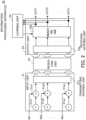
- FIG. 2 illustrates an example of an information processing apparatus according to a second embodiment.
- the information processing apparatus 20 of the second embodiment includes an input unit 21, a reservoir unit 22, an output unit 23, and a learning unit 24.
- the input unit 21 includes high-frequency power sources 21a1, 21a2, ..., 21an, multipliers 21b1, 21b2, ..., 21bn, and a transmitting antenna unit 21c.
- the high-frequency power sources 21a1 to 21an output high-frequency signals.
- the high-frequency signals output from the high-frequency power sources 21a1 to 21an have the same frequency.
- the number of high-frequency power sources 21a1 to 21an may be one, and a high-frequency signal from one high-frequency power source may be supplied in common to the multipliers 21b1 to 21bn.
- Each of the multipliers 21b1 to 21bn outputs the product of a received high-frequency signal and a corresponding one of input signals IN1, IN2, ..., INn. Thereby, the strengths (amplitudes) of the n high-frequency signals output from the multipliers 21b1 to 21bn respectively reflect the input signals IN1 to INn.
- the transmitting antenna unit 21c includes an antenna that converts the high-frequency signals output from the multipliers 21b1 to 21bn into radio waves and emits the radio waves.
- a plurality of antennas may be provided, and the number of antennas does not need to match the number of input signals IN1 to INn (the number of multipliers 21b1 to 21bn).
- a high-frequency signal output from one of the multipliers 21b1 to 21bn may be input to the plurality of antennas, or high-frequency signals output from the plurality of multipliers may be input to one antenna.
- An example of the antenna will be described later.
- the reservoir unit 22 outputs radio waves obtained by modulating the radio waves emitted from the antenna of the input unit 21.
- the reservoir unit 22 includes a plurality of semiconductor elements that modulate the radio waves emitted from the input unit 21 by exhibiting non-linear response to the radio waves. An example of the reservoir unit 22 will be described later.
- the output unit 23 includes a receiving antenna unit 23a and a weighting unit 23b.
- the receiving antenna unit 23a receives the radio waves modulated by the reservoir unit 22 and converts the received radio waves into high-frequency signals.
- the output unit 13 has one or more antennas according to the number of high-frequency signals into which the received radio waves are converted, and converts the received radio waves into high-frequency signals with the antennas.
- the weighting unit 23b weights direct current signals obtained by converting the high-frequency signals and outputs the weighted signals or signals by adding the plurality of weighted signals as output signals OUT1, OUT2, ..., OUTn.
- the number of output signals OUT1 to OUTn does not need to match the number of antennas provided in the receiving antenna unit 23a.
- the number of output signals OUT1 to OUTn does not need to match the number of input signals IN1 to INn.
- the number of output signals OUT1 to OUTn may be one.
- the learning unit 24 obtains teacher data and adjusts the magnitude of the weighting performed by the weighting unit 23b on the basis of the teacher data and the output signals OUT1 to OUTn of the output unit 23.
- weighting unit 23b and learning unit 24 Examples of the weighting unit 23b and learning unit 24 will be described later.
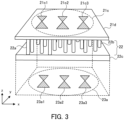
- FIG. 3 illustrates an example of the transmitting antenna unit, reservoir unit, and receiving antenna unit.
- the transmitting antenna unit 21c includes bowtie antennas 21c1, 21c2, and 21c3. Each bowtie antenna 21c1 to 21c3 is formed by a pair of electrodes whose triangles have apices facing each other. The bowtie antennas 21c1 to 21c3 are formed on a substrate 21d.
- the use of the bowtie antennas 21c1 to 21c3 makes it possible to emit radio waves obtained by converting high-frequency signals to the reservoir unit 22 efficiently because of a bowtie antenna effect.
- the reservoir unit 22 illustrated in FIG. 3 includes a plurality of InAs semiconductor nanowires (InAs semiconductor nanowires 22a and 22b and others, for example) as the plurality of semiconductor elements that exhibit non-linear response.
- the plurality of InAs semiconductor nanowires are formed on a substrate 22c such as a silicon (Si) substrate so as to extend in the z direction by crystal growth.
- the InAs semiconductor nanowires may be arranged regularly on the substrate 22c, but may preferably be arranged randomly in order to increase the diversity of the random network.
- the length of a semiconductor element in the long axis direction is preferably greater than or equal to 1/10 the effective wavelength of a high-frequency signal (the value obtained by dividing the wavelength by the refractive index of the semiconductor element), because such a semiconductor element itself has a remarkable antenna effect and has a stronger interaction with the high-frequency signal.
- nanowires such as InAs semiconductor nanowires have a wire length of several um to 100 ⁇ m. Assuming microwave and terahertz-wave high-frequency signals, such high-frequency signals have a wavelength of several hundred um to several cm. Therefore, in the case of using nanowires, the longer in the long axis direction, the more preferred. Especially, in the case where the wire length in the long axis direction is greater than or equal to 1/10 the effective wavelength of a high-frequency signal, as described above, the nanowires themselves have a remarkable antenna effect.
- the reservoir unit 22 with high performance may be implemented with fewer InAs semiconductor nanowires.
- the InAs semiconductor nanowires need to be formed with a density that is 10 times as high as that in the case with a wire length of 34 ⁇ m, in order to achieve the same performance.
- the reservoir unit 22 is spatially separated from the input unit 21 including the transmitting antenna unit 21c by the substrate 21d, and is also spatially separated from the output unit 23 including the receiving antenna unit 23a by the substrate 22c.
- a plurality of regions where semiconductor elements as described above are formed may be layered in the z direction.
- a plurality of layers where InAs semiconductor nanowires are formed on the substrate 22c by crystal growth in the z direction may be layered in the z direction. This makes it possible to configure a large-scale random network.
- an area where semiconductor elements are sparsely arranged and an area where semiconductor elements are densely arranged may coexist.
- FIG. 4 illustrates an example in which the reservoir unit has both a dense area of semiconductor elements and a sparse area of semiconductor elements.
- nanowire diodes of pn hetero junction type such as p-GaAs/n-InAs, with stronger non-linearity than the InAs semiconductor nanowires may be used as the nanowires.
- FIG. 5 illustrates an example of a reservoir unit using nanowire diodes.
- the nanowire diodes are each formed by joining a p-type semiconductor 22d1 and an n-type semiconductor 22d2.
- the p-type semiconductor 22d1 is p-type GaAs
- the n-type semiconductor 22d2 is n-type InAs.
- the nanowire diodes exhibit strong non-linearity and therefore enable the reservoir unit 22 to have higher performance.
- carbon nanotubes may be used as an example of the one-dimensional semiconductors.
- the receiving antenna unit 23a includes bowtie antennas 23a1, 23a2, and 23a3.
- the bowtie antennas 23a1 to 23a3 are formed on the rear surface of the substrate 22c that has InAs semiconductor nanowires formed on the front surface thereof.
- bowtie antennas 23a1 to 23a3 makes it possible to receive high-frequency signals converted into radio waves from the reservoir unit 22 efficiently because of a bowtie antenna effect.
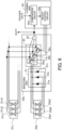
- FIG. 6 illustrates an example of the weighting unit and learning unit.
- FIG. 6 illustrates an example of generating one output signal OUT1 from high-frequency signals obtained through conversion by three bowtie antennas 23a1 to 23a3, for simple description.
- the weighting unit 23b includes a direct current (DC) conversion unit 31, weight adjustment unit 32, and an addition unit 33.
- DC direct current
- the DC conversion unit 31 converts high-frequency signals obtained by converting radio waves with the receiving antenna unit 23a, into direct current signals (direct-current voltage or current amplitude signals).
- the DC conversion unit 31 includes diodes 31a, 31b, and 31c.
- the anode of the diode 31a is connected to one of the pair of electrodes of the bowtie antenna 23a3, and the cathode of the diode 31a is connected to the other of the pair of electrodes of the bowtie antenna 23a3.
- the anode of the diode 31b is connected to one of the pair of electrodes of the bowtie antenna 23a2, and the cathode of the diode 31b is connected to the other of the pair of electrodes of the bowtie antenna 23a2.
- the anode of the diode 31c is connected to one of the pair of electrodes of the bowtie antenna 23a1, and the cathode of the diode 31c is connected to the other of the pair of electrodes of the bowtie antenna 23a1.
- Direct current signals respectively output from the cathodes of the diodes 31a, 31b, and 31c are outputs of the DC conversion unit 31.
- the weight adjustment unit 32 weights the direct current signals output from the DC conversion unit 31. The magnitude of the weighting is adjusted by the learning unit 24.
- the weight adjustment unit 32 includes memristors (variable resistance memories) 32a, 32b, and 32c as an example of analog memories holding the magnitude of the weighting.
- the direct current signals output from the cathodes of the diodes 31a, 31b, and 31c are respectively weighted according to the magnitudes of the resistances of the memristors 32a, 32b, and 32c controlled by the learning unit 24.
- the addition unit 33 outputs the result of adding the weighted direct current signals as the output signal OUT1, which is a computation result of the information processing apparatus 20.
- the outputs of the weight adjustment unit 32 or signals subjected to attenuation at a fixed rate by resistors, not illustrated, are respectively added to high-frequency signals that propagate through the signal lines connected to the bowtie antennas 21c1 to 21c3 provided at the input stage.
- an input is made such that a past output is directly associated with the current input.
- the use of the feedback loops makes it possible to achieve high speed training.
- the weighting unit 23b as described above may be formed on the same plane as where the bowtie antennas 23a1 to 23a3 are formed on the substrate 22c illustrated in FIG. 3 .
- the learning unit 24 includes a comparison circuit 24a and a weight control circuit 24b.
- the comparison circuit 24a outputs a comparison result (for example, an error) of comparing received teacher data with the output signal OUT1.
- the weight control circuit 24b adjusts the magnitude of the weighting (for example, the magnitudes of the resistances of the memristors 32a, 32b, and 32c) in the weighting unit 23b so as to minimize the error.
- the learning unit 24 is cut off from the weighting unit 23b by using a switch or the like, not illustrated.
- the learning unit 24 may be a computer that is implemented by using a processor or the like that is a hardware component such as a central processing unit (CPU) or a digital signal processor (DSP).
- the learning unit 24 may include an application specific electronic circuit such as an application specific integrated circuit (ASIC) or field programmable gate array (FPGA).
- the processor executes programs stored in a memory such as a random access memory (RAM) to control the magnitude of weighting on the basis of the comparison result of comparing the teacher data with the output signal OUT1.
- RAM random access memory
- the following describes a flow of a computational process of the information processing apparatus 20 according to the second embodiment.
- FIG. 7 is a flowchart illustrating an example flow of a computational process of the information processing apparatus according to the second embodiment.
- the input unit 21 receives inputs of input signals IN1 to INn (step S1).
- the transmitting antenna unit 21c converts high-frequency signals reflecting the input signals IN1 to INn into radio waves and emits the radio waves (step S2).
- the reservoir unit 22 modulates the radio waves emitted from the input unit 21 by exhibiting non-linear response to the radio waves (step S3).
- the receiving antenna unit 23a receives the radio waves modulated by the reservoir unit 22 and converts the received radio waves into high-frequency signals (step S4).
- the weighting unit 23b in the output unit 23 weights the direct current signals obtained by converting the high-frequency signals (step S5).
- the output unit 23 outputs the weighted signals or signals obtained by adding the plurality of weighted signals as the output signals OUT1 to OUTn that indicate a computation result (step S6). Then, the information processing apparatus 20 completes the computational process.
- the above-described information processing apparatus 20 eliminates the need of wiring in the reservoir unit 22, which makes it possible to improve the integration density with a simple process. It is thus expected to improve the performance of a reservoir computer, such as simplifying the configuration of a large-scale random network for it.
Landscapes
- Engineering & Computer Science (AREA)
- Physics & Mathematics (AREA)
- Theoretical Computer Science (AREA)
- Health & Medical Sciences (AREA)
- Life Sciences & Earth Sciences (AREA)
- Biomedical Technology (AREA)
- Biophysics (AREA)
- General Health & Medical Sciences (AREA)
- Data Mining & Analysis (AREA)
- Evolutionary Computation (AREA)
- Computational Linguistics (AREA)
- Molecular Biology (AREA)
- Computing Systems (AREA)
- General Engineering & Computer Science (AREA)
- General Physics & Mathematics (AREA)
- Mathematical Physics (AREA)
- Software Systems (AREA)
- Artificial Intelligence (AREA)
- Neurology (AREA)
- Variable-Direction Aerials And Aerial Arrays (AREA)
Abstract
Description
- The embodiments discussed herein relate to an information processing apparatus and an information processing method.
- As one of computing systems for artificial intelligence (AI), a reservoir computing system, which is a type of recurrent neural network (RNN), is known (see, for example, PTL1). The reservoir computing system includes a network-type device that is formed of non-linear elements and is called a reservoir.
- There is a conventional technique of implementing a reservoir with complementary metal-oxide-semiconductor (CMOS) devices. In addition, there is a proposal of implementing a reservoir using a random network of carbon nanotubes (see, for example, NPTL1).
- Further, there is a conventional technique of communicating signals between neurons using radio waves in a neural network (for example, PTL2).
-
- [PTL1]
Japanese Laid-open Patent Publication No. 2018-180701 - [PTL2]
Japanese Laid-open Patent Publication No. H06-243117 - [NPTL1] Hirofumi Tanaka et al., "A molecular neuromorphic network device consisting of single-walled carbon nanotubes complexed with polyoxometalate", Nature Communications volume 9, Article number: 2693, 2018
- In a reservoir computing system, when an improvement in the integration density of an apparatus is achieved, it becomes possible to improve the performance of a reservoir, such as simplifying the configuration of a large-scale random network for the reservoir. In the case of implementing the reservoir with CMOS devices, however, it is difficult to improve the integration density due to an increase in the number of components and complexity of wiring. In addition, the conventional technique of implementing a reservoir using carbon nanotubes needs to electrically connect the carbon nanotubes so as to cause the carbon nanotubes to function as conductive wires, which makes it difficult to improve the integration density and thus to configure multiple terminal inputs and a large-scale random network.
- According to one aspect, the present disclosure intends to provide an information processing apparatus including a reservoir unit and an information processing method that enable an improvement in the integration density of an apparatus.
- According to one aspect, there is provided an information processing apparatus including: an input unit that converts a first high-frequency signal into a first radio wave and emits the first radio wave; an output unit that converts a received second radio wave into a second high-frequency signal; and a reservoir unit that is provided between the input unit and the output unit, that includes a plurality of semiconductor elements for modulating the first radio wave by exhibiting non-linear response to the first radio wave, and that outputs the second radio wave obtained by modulating the first radio wave.
- Further, according to one aspect, there is provided an information processing method.
- According to one aspect, the present disclosure makes it possible to improve the integration density of an information processing apparatus including a reservoir unit.
- The above and other objects, features and advantages of the present invention will become apparent from the following description read in conjunction with the accompanying drawings representing preferred embodiments.
-
- [
FIG. 1] FIG. 1 illustrates an example of an information processing apparatus according to a first embodiment. - [
FIG. 2] FIG. 2 illustrates an example of an information processing apparatus according to a second embodiment. - [
FIG. 3] FIG. 3 illustrates an example of a transmitting antenna unit, reservoir unit, and receiving antenna unit. - [
FIG. 4] FIG. 4 illustrates an example in which the reservoir unit has both a dense area of semiconductor elements and a sparse area of semiconductor elements. - [
FIG. 5] FIG. 5 illustrates an example of the reservoir unit using nanowire diodes. - [
FIG. 6] FIG. 6 illustrates an example of a weighting unit and learning unit. - [
FIG. 7] FIG. 7 is a flowchart illustrating an example flow of a computational process of the information processing apparatus according to the second embodiment. - Hereinafter, embodiments will be described in detail with reference to the accompanying drawings.
-
FIG. 1 illustrates an example of an information processing apparatus according to a first embodiment. - The
information processing apparatus 10 according to the first embodiment functions as a reservoir computer, and includes aninput unit 11, areservoir unit 12, and anoutput unit 13. - The
input unit 11 converts high-frequency signals into radio waves and emits the radio waves. For example, the high-frequency signals are microwave signals or terahertz-wave signals. Theinput unit 11 includes one or more antennas according to the number of high-frequency signals to be converted into radio waves, and converts the high-frequency signals into the radio waves with the antennas. In this connection, for example, a high-frequency signal has an amplitude based on the value of an input signal. The input signal is a signal based on a problem to be computed and is, for example, a signal with a value of 1 or 0, a sine wave signal, or another. - The
reservoir unit 12 is provided between theinput unit 11 and theoutput unit 13, and outputs radio waves obtained by modulating the radio waves emitted from theinput unit 11. Thereservoir unit 12 includes a plurality of semiconductor elements that modulate the radio waves emitted from theinput unit 11 by exhibiting non-linear response to the radio waves. - For example, each of the plurality of semiconductor elements that exhibit the non-linear response is a one-dimensional semiconductor or a two-dimensional layered semiconductor.
- As the one-dimensional semiconductors, nanowires (for example, indium arsenic (InAs) semiconductor nanowires) may be used. In addition, pn hetero nanowires (also called nanowire diodes), such as p-GaAs (gallium arsenic)/n-InAs, with stronger non-linearity than InAs semiconductor nanowires may be used as the one-dimensional semiconductors. Alternatively, carbon nanotubes may be used as the one-dimensional semiconductors.
- As the two-dimensional layered semiconductors, graphene nanoribbons and others are used, for example.
-
FIG. 1 illustrates an example of using a plurality of one-dimensional semiconductors (one-dimensional semiconductors reservoir unit 12. - The
output unit 13 receives the radio waves (obtained by modulation) output from thereservoir unit 12, and converts the received radio waves into high-frequency signals. For example, theoutput unit 13 includes one or more antennas according to the number of high-frequency signals to be output, and converts the received radio waves into the high-frequency signals with the antennas. Theoutput unit 13 outputs a computation result based on the amplitudes of the high-frequency signals. For example, theoutput unit 13 converts the plurality of high-frequency signals obtained by the plurality of antennas into direct current signals, weights each direct current signal by a weight value obtained by training, and outputs a value obtained by adding these as the computation result of theinformation processing apparatus 10. For example, the computation result is an inference result in the case where the problem to be computed is a problem to infer something, or is a classification result in the case where the problem to be computed is a problem to classify something. - With the
information processing apparatus 10 as described above, the signal processing of thereservoir unit 12 that functions as a neural network using fixed values as the weight values (also called coupling coefficients) between neurons is performed using radio waves that propagate in a space. More specifically, high-frequency signals are converted into radio waves by theinput unit 11, and the converted radio waves are modulated through non-linear response by the plurality of semiconductor elements of thereservoir unit 12 and are converted back to high-frequency signals by theoutput unit 13. Thisinformation processing apparatus 10 is equivalent to a reservoir computing device having wire connections. However, theinformation processing apparatus 10 does not need wiring in thereservoir unit 12, which makes it possible to improve the integration density with a simple process. It is thus expected to improve the performance of the reservoir computer, such as simplifying the configuration of a large-scale random network for it. - In addition, the plurality of semiconductor elements may be configured to have different sizes (for example, one-dimensional semiconductors may have different lengths in the long axis direction) (this may be achieved using manufacturing variance), or the
reservoir unit 12 may be provided with an area where semiconductor elements are sparsely arranged and an area where semiconductor elements are densely arranged. This enables an increase in the diversity of the random network, so as to implement the reservoir computer with higher performance. - In addition, in the case of using one-dimensional semiconductors as the semiconductor elements, the antenna effect of the semiconductor elements themselves causes sufficient interaction between the semiconductor elements that are nodes of the random network and propagating radio waves, which enables the
reservoir unit 12 to perform signal processing similar to that in the case of using network-type elements. - In this connection, reservoir computing performs training by adjusting weight values for output signals of a reservoir layer. Likewise, the above-described
information processing apparatus 10 is able to perform training by adjusting the weight values for the direct current signals obtained by converting the high-frequency signals obtained from the radio waves output from thereservoir unit 12. A configuration example for the training will be described later. -
FIG. 2 illustrates an example of an information processing apparatus according to a second embodiment. - The
information processing apparatus 20 of the second embodiment includes aninput unit 21, areservoir unit 22, anoutput unit 23, and alearning unit 24. - The
input unit 21 includes high-frequency power sources 21a1, 21a2, ..., 21an, multipliers 21b1, 21b2, ..., 21bn, and a transmittingantenna unit 21c. - The high-frequency power sources 21a1 to 21an output high-frequency signals. The high-frequency signals output from the high-frequency power sources 21a1 to 21an have the same frequency. In this connection, the number of high-frequency power sources 21a1 to 21an may be one, and a high-frequency signal from one high-frequency power source may be supplied in common to the multipliers 21b1 to 21bn.
- Each of the multipliers 21b1 to 21bn outputs the product of a received high-frequency signal and a corresponding one of input signals IN1, IN2, ..., INn. Thereby, the strengths (amplitudes) of the n high-frequency signals output from the multipliers 21b1 to 21bn respectively reflect the input signals IN1 to INn.
- The transmitting
antenna unit 21c includes an antenna that converts the high-frequency signals output from the multipliers 21b1 to 21bn into radio waves and emits the radio waves. - In this connection, a plurality of antennas may be provided, and the number of antennas does not need to match the number of input signals IN1 to INn (the number of multipliers 21b1 to 21bn). For example, a high-frequency signal output from one of the multipliers 21b1 to 21bn may be input to the plurality of antennas, or high-frequency signals output from the plurality of multipliers may be input to one antenna. An example of the antenna will be described later.
- The
reservoir unit 22 outputs radio waves obtained by modulating the radio waves emitted from the antenna of theinput unit 21. Thereservoir unit 22 includes a plurality of semiconductor elements that modulate the radio waves emitted from theinput unit 21 by exhibiting non-linear response to the radio waves. An example of thereservoir unit 22 will be described later. - The
output unit 23 includes a receivingantenna unit 23a and aweighting unit 23b. - The receiving
antenna unit 23a receives the radio waves modulated by thereservoir unit 22 and converts the received radio waves into high-frequency signals. For example, theoutput unit 13 has one or more antennas according to the number of high-frequency signals into which the received radio waves are converted, and converts the received radio waves into high-frequency signals with the antennas. - The
weighting unit 23b weights direct current signals obtained by converting the high-frequency signals and outputs the weighted signals or signals by adding the plurality of weighted signals as output signals OUT1, OUT2, ..., OUTn. - In this connection, the number of output signals OUT1 to OUTn does not need to match the number of antennas provided in the receiving
antenna unit 23a. In addition, the number of output signals OUT1 to OUTn does not need to match the number of input signals IN1 to INn. For example, the number of output signals OUT1 to OUTn may be one. - The
learning unit 24 obtains teacher data and adjusts the magnitude of the weighting performed by theweighting unit 23b on the basis of the teacher data and the output signals OUT1 to OUTn of theoutput unit 23. - Examples of the
weighting unit 23b andlearning unit 24 will be described later. -
FIG. 3 illustrates an example of the transmitting antenna unit, reservoir unit, and receiving antenna unit. - The transmitting
antenna unit 21c includes bowtie antennas 21c1, 21c2, and 21c3. Each bowtie antenna 21c1 to 21c3 is formed by a pair of electrodes whose triangles have apices facing each other. The bowtie antennas 21c1 to 21c3 are formed on asubstrate 21d. - The use of the bowtie antennas 21c1 to 21c3 makes it possible to emit radio waves obtained by converting high-frequency signals to the
reservoir unit 22 efficiently because of a bowtie antenna effect. - The
reservoir unit 22 illustrated inFIG. 3 includes a plurality of InAs semiconductor nanowires (InAs semiconductor nanowires substrate 22c such as a silicon (Si) substrate so as to extend in the z direction by crystal growth. - In this connection, the InAs semiconductor nanowires may be arranged regularly on the
substrate 22c, but may preferably be arranged randomly in order to increase the diversity of the random network. - Note that, in the semiconductor elements that exhibit non-linear response to high-frequency signals converted into radio waves, their strengths of the interactions with the high-frequency signals depend on their lengths in the long axis direction. As the interactions become stronger, the
reservoir unit 22 has higher performance. - Especially, the length of a semiconductor element in the long axis direction is preferably greater than or equal to 1/10 the effective wavelength of a high-frequency signal (the value obtained by dividing the wavelength by the refractive index of the semiconductor element), because such a semiconductor element itself has a remarkable antenna effect and has a stronger interaction with the high-frequency signal.
- In general, nanowires such as InAs semiconductor nanowires have a wire length of several um to 100 µm. Assuming microwave and terahertz-wave high-frequency signals, such high-frequency signals have a wavelength of several hundred um to several cm. Therefore, in the case of using nanowires, the longer in the long axis direction, the more preferred. Especially, in the case where the wire length in the long axis direction is greater than or equal to 1/10 the effective wavelength of a high-frequency signal, as described above, the nanowires themselves have a remarkable antenna effect. Therefore, for example, in the case where a minimum frequency of 250 GHz (a wavelength of 1200 µm) is set for the frequencies of the high-frequency signals, the wire lengths of the InAs semiconductor nanowires may be set to 1200/(3.5 × 10) = 34 (µm) or more, considering that InAs has a refractive index of 3.5.
- With this, the
reservoir unit 22 with high performance may be implemented with fewer InAs semiconductor nanowires. For example, in the case of using InAs semiconductor nanowires with a wire length of 3.4 µm, the InAs semiconductor nanowires need to be formed with a density that is 10 times as high as that in the case with a wire length of 34 µm, in order to achieve the same performance. - The
reservoir unit 22 is spatially separated from theinput unit 21 including the transmittingantenna unit 21c by thesubstrate 21d, and is also spatially separated from theoutput unit 23 including the receivingantenna unit 23a by thesubstrate 22c. - In this connection, in the
reservoir unit 22, a plurality of regions where semiconductor elements as described above are formed may be layered in the z direction. For example, a plurality of layers where InAs semiconductor nanowires are formed on thesubstrate 22c by crystal growth in the z direction may be layered in the z direction. This makes it possible to configure a large-scale random network. - In addition, in the
reservoir unit 22, an area where semiconductor elements are sparsely arranged and an area where semiconductor elements are densely arranged may coexist. -
FIG. 4 illustrates an example in which the reservoir unit has both a dense area of semiconductor elements and a sparse area of semiconductor elements. - In the example of
FIG. 4 , an area where InAs semiconductor nanowires (InAs semiconductor nanowire 22a and others) are densely arranged and an area where InAs semiconductor nanowires are sparsely arranged coexist. - This enables an increase in the diversity of the random network, so as to implement the reservoir computer with higher performance.
- Note that, in place of the InAs semiconductor nanowires, nanowire diodes of pn hetero junction type, such as p-GaAs/n-InAs, with stronger non-linearity than the InAs semiconductor nanowires may be used as the nanowires.
-
FIG. 5 illustrates an example of a reservoir unit using nanowire diodes. - The nanowire diodes are each formed by joining a p-type semiconductor 22d1 and an n-type semiconductor 22d2. For example, the p-type semiconductor 22d1 is p-type GaAs, whereas the n-type semiconductor 22d2 is n-type InAs.
- The nanowire diodes exhibit strong non-linearity and therefore enable the
reservoir unit 22 to have higher performance. - In this connection, carbon nanotubes may be used as an example of the one-dimensional semiconductors.
- Referring to
FIG. 3 , the receivingantenna unit 23a includes bowtie antennas 23a1, 23a2, and 23a3. The bowtie antennas 23a1 to 23a3 are formed on the rear surface of thesubstrate 22c that has InAs semiconductor nanowires formed on the front surface thereof. - The use of the bowtie antennas 23a1 to 23a3 makes it possible to receive high-frequency signals converted into radio waves from the
reservoir unit 22 efficiently because of a bowtie antenna effect. -
FIG. 6 illustrates an example of the weighting unit and learning unit. - In this connection,
FIG. 6 illustrates an example of generating one output signal OUT1 from high-frequency signals obtained through conversion by three bowtie antennas 23a1 to 23a3, for simple description. - The
weighting unit 23b includes a direct current (DC)conversion unit 31,weight adjustment unit 32, and anaddition unit 33. - The
DC conversion unit 31 converts high-frequency signals obtained by converting radio waves with the receivingantenna unit 23a, into direct current signals (direct-current voltage or current amplitude signals). - Referring to the example of
FIG. 6 , theDC conversion unit 31 includesdiodes diode 31a is connected to one of the pair of electrodes of the bowtie antenna 23a3, and the cathode of thediode 31a is connected to the other of the pair of electrodes of the bowtie antenna 23a3. The anode of thediode 31b is connected to one of the pair of electrodes of the bowtie antenna 23a2, and the cathode of thediode 31b is connected to the other of the pair of electrodes of the bowtie antenna 23a2. The anode of thediode 31c is connected to one of the pair of electrodes of the bowtie antenna 23a1, and the cathode of thediode 31c is connected to the other of the pair of electrodes of the bowtie antenna 23a1. Direct current signals respectively output from the cathodes of thediodes DC conversion unit 31. - The
weight adjustment unit 32 weights the direct current signals output from theDC conversion unit 31. The magnitude of the weighting is adjusted by thelearning unit 24. - In
FIG. 6 , theweight adjustment unit 32 includes memristors (variable resistance memories) 32a, 32b, and 32c as an example of analog memories holding the magnitude of the weighting. The direct current signals output from the cathodes of thediodes memristors learning unit 24. - The
addition unit 33 outputs the result of adding the weighted direct current signals as the output signal OUT1, which is a computation result of theinformation processing apparatus 20. - In this connection, as illustrated in
FIG. 6 , for example, the outputs of theweight adjustment unit 32 or signals subjected to attenuation at a fixed rate by resistors, not illustrated, are respectively added to high-frequency signals that propagate through the signal lines connected to the bowtie antennas 21c1 to 21c3 provided at the input stage. With such a feedback loop, an input is made such that a past output is directly associated with the current input. For example, in training with time-series data, it is possible to perform the training so as to highly reflect the temporal correlation. That is, for a problem in which training for the temporal correlation dominates the performance, the use of the feedback loops makes it possible to achieve high speed training. In this connection, it is possible to activate or deactivate the feedback loops individually by using switches or the like, not illustrated. - For example, the
weighting unit 23b as described above may be formed on the same plane as where the bowtie antennas 23a1 to 23a3 are formed on thesubstrate 22c illustrated inFIG. 3 . - The
learning unit 24 includes acomparison circuit 24a and aweight control circuit 24b. Thecomparison circuit 24a outputs a comparison result (for example, an error) of comparing received teacher data with the output signal OUT1. - On the basis of the comparison result, the
weight control circuit 24b adjusts the magnitude of the weighting (for example, the magnitudes of the resistances of thememristors weighting unit 23b so as to minimize the error. - In this connection, after the training is complete, the
learning unit 24 is cut off from theweighting unit 23b by using a switch or the like, not illustrated. - The
learning unit 24 may be a computer that is implemented by using a processor or the like that is a hardware component such as a central processing unit (CPU) or a digital signal processor (DSP). In this connection, thelearning unit 24 may include an application specific electronic circuit such as an application specific integrated circuit (ASIC) or field programmable gate array (FPGA). The processor executes programs stored in a memory such as a random access memory (RAM) to control the magnitude of weighting on the basis of the comparison result of comparing the teacher data with the output signal OUT1. - The following describes a flow of a computational process of the
information processing apparatus 20 according to the second embodiment. -
FIG. 7 is a flowchart illustrating an example flow of a computational process of the information processing apparatus according to the second embodiment. - The
input unit 21 receives inputs of input signals IN1 to INn (step S1). - Then, in the
input unit 21, the transmittingantenna unit 21c converts high-frequency signals reflecting the input signals IN1 to INn into radio waves and emits the radio waves (step S2). - The
reservoir unit 22 modulates the radio waves emitted from theinput unit 21 by exhibiting non-linear response to the radio waves (step S3). - In the
output unit 23, the receivingantenna unit 23a receives the radio waves modulated by thereservoir unit 22 and converts the received radio waves into high-frequency signals (step S4). - In addition, the
weighting unit 23b in theoutput unit 23 weights the direct current signals obtained by converting the high-frequency signals (step S5). - Then, the
output unit 23 outputs the weighted signals or signals obtained by adding the plurality of weighted signals as the output signals OUT1 to OUTn that indicate a computation result (step S6). Then, theinformation processing apparatus 20 completes the computational process. - As with the
information processing apparatus 10 of the first embodiment, the above-describedinformation processing apparatus 20 eliminates the need of wiring in thereservoir unit 22, which makes it possible to improve the integration density with a simple process. It is thus expected to improve the performance of a reservoir computer, such as simplifying the configuration of a large-scale random network for it. - The above description is merely indicative of the principles of the present embodiments. A wide variety of modifications and changes may also be made by those skilled in the art. The present embodiments are not limited to the precise configurations and example applications indicated and described above, and all appropriate modifications and equivalents are regarded as falling within the scope of the embodiments as defined by the appended patent claims and their equivalents.
-
- 10 Information processing apparatus
- 11 Input unit
- 12 Reservoir unit
- 12a, 12b One-dimensional semiconductor
- 13 Output unit
Claims (8)
- An information processing apparatus comprising:an input unit that converts a first high-frequency signal into a first radio wave and emits the first radio wave;an output unit that converts a received second radio wave into a second high-frequency signal; anda reservoir unit that is provided between the input unit and the output unit, that includes a plurality of semiconductor elements for modulating the first radio wave by exhibiting non-linear response to the first radio wave, and that outputs the second radio wave obtained by modulating the first radio wave.
- The information processing apparatus according to claim 1, wherein each of the plurality of semiconductor elements is a one-dimensional semiconductor or a two-dimensional layered semiconductor.
- The information processing apparatus according to claim 2, wherein the one-dimensional semiconductor is a nanowire diode.
- The information processing apparatus according to any one of claims 1 to 3, wherein, in the reservoir unit, an area where some of the plurality of semiconductor elements are sparsely arranged and an area where some of the plurality of semiconductor elements are densely arranged coexist.
- The information processing apparatus according to any one of claims 1 to 4, wherein the input unit or the output unit includes one or more bowtie antennas.
- The information processing apparatus according to any one of claims 1 to 5, wherein the output unit converts the second high-frequency signal into a direct current signal and weights the direct current signal.
- The information processing apparatus according to claim 6, further comprisinga learning unit that adjusts a magnitude of weighting for the direct current signal, based on teacher data, whereinthe input unit adds the weighted direct current signal to the first high-frequency signal.
- An information processing method comprising:converting, by an input unit, a first high-frequency signal into a first radio wave and emitting the first radio wave;outputting, by a reservoir unit including a plurality of semiconductor elements for modulating the first radio wave by exhibiting non-linear response to the first radio wave, a second radio wave obtained by modulating the first radio wave; andconverting, by an output unit, the second radio wave received into a second high-frequency signal.
Applications Claiming Priority (1)
| Application Number | Priority Date | Filing Date | Title |
|---|---|---|---|
| PCT/JP2020/026580 WO2022009314A1 (en) | 2020-07-07 | 2020-07-07 | Information processing device and information processing method |
Publications (3)
| Publication Number | Publication Date |
|---|---|
| EP4181023A1 true EP4181023A1 (en) | 2023-05-17 |
| EP4181023A4 EP4181023A4 (en) | 2023-07-12 |
| EP4181023B1 EP4181023B1 (en) | 2024-07-17 |
Family
ID=79552330
Family Applications (1)
| Application Number | Title | Priority Date | Filing Date |
|---|---|---|---|
| EP20944413.2A Active EP4181023B1 (en) | 2020-07-07 | 2020-07-07 | Information processing device and information processing method |
Country Status (4)
| Country | Link |
|---|---|
| US (1) | US20230117769A1 (en) |
| EP (1) | EP4181023B1 (en) |
| JP (1) | JP7425370B2 (en) |
| WO (1) | WO2022009314A1 (en) |
Family Cites Families (4)
| Publication number | Priority date | Publication date | Assignee | Title |
|---|---|---|---|---|
| JPH06243117A (en) * | 1993-02-18 | 1994-09-02 | Fuji Xerox Co Ltd | Neural network system |
| EP2821942B1 (en) * | 2013-07-05 | 2020-11-04 | Universiteit Gent | Reservoir computing using passive optical systems |
| JP6791800B2 (en) | 2017-04-05 | 2020-11-25 | 株式会社日立製作所 | Calculation method using computer system and recurrent neural network |
| US10211856B1 (en) * | 2017-10-12 | 2019-02-19 | The Boeing Company | Hardware scalable channelizer utilizing a neuromorphic approach |
-
2020
- 2020-07-07 JP JP2022534539A patent/JP7425370B2/en active Active
- 2020-07-07 WO PCT/JP2020/026580 patent/WO2022009314A1/en not_active Ceased
- 2020-07-07 EP EP20944413.2A patent/EP4181023B1/en active Active
-
2022
- 2022-12-16 US US18/082,612 patent/US20230117769A1/en active Pending
Also Published As
| Publication number | Publication date |
|---|---|
| JP7425370B2 (en) | 2024-01-31 |
| JPWO2022009314A1 (en) | 2022-01-13 |
| WO2022009314A1 (en) | 2022-01-13 |
| EP4181023B1 (en) | 2024-07-17 |
| US20230117769A1 (en) | 2023-04-20 |
| EP4181023A4 (en) | 2023-07-12 |
Similar Documents
| Publication | Publication Date | Title |
|---|---|---|
| US6611223B2 (en) | Method and apparatus for ultra wide-band communication system using multiple detectors | |
| CN110535486B (en) | Radio Frequency Signal Direct Processing Wireless Transceiver Based on Metasurface Neural Network | |
| Hua et al. | Sine-transform-based chaotic system with FPGA implementation | |
| CN110649976B (en) | Device and method for position measurement and reading suitable for multiple quantum computer chips | |
| JP2021535596A (en) | Antenna chip structure for qubit annealing | |
| Xiao et al. | Data-based model for wide nulling problem in adaptive digital beamforming antenna array | |
| US10891536B1 (en) | Artificial neural network for reservoir computing using stochastic logic | |
| WO2018213399A1 (en) | Integrated circuit designs for reservoir computing and machine learning | |
| US20190305583A1 (en) | Energy harvest terminal | |
| EP3393083B1 (en) | Method and device for configuring a data transmission and processing system | |
| US11790220B2 (en) | Artificial neural networks | |
| CN103023839B (en) | Radio optical communication system blind balance method based on the output multiply-connected continuous Feedback Neural Network structure of feedback biasing type | |
| EP4181023B1 (en) | Information processing device and information processing method | |
| CN113922097A (en) | Electromagnetic wave time-space frequency domain modulation method based on digital programmable transmission type super surface | |
| US10649068B2 (en) | Method for modulating a microwave frequency wave, transmission system carrying out this method, and radar comprising a system of this type | |
| Günay et al. | A performance comparison study of programmable platforms: FPAA and FPGA implementation of COOK communication system | |
| Rácz et al. | A full-stack neuromorphic prototype architecture for low-power wireless sensors | |
| Hirose et al. | Coherent optical associative memory system that processes complex-amplitude information | |
| US9537516B1 (en) | Edge combining transmitter | |
| US11777447B2 (en) | Oscillation circuit and information processing device | |
| WO2021124379A1 (en) | Reservoir element | |
| Hjortland | Sampled and continuous-time 1-bit signal processing in CMOS for wireless sensor networks | |
| US20240330668A1 (en) | Analogue arithmetic unit and nuromorphic device | |
| Benhamou et al. | Waveform Optimization Techniques for Energy Transfer Systems: A Novel Approach to Improving Performance | |
| Kavitha | Foundations of Electronics and Communication Engineering |
Legal Events
| Date | Code | Title | Description |
|---|---|---|---|
| STAA | Information on the status of an ep patent application or granted ep patent |
Free format text: STATUS: THE INTERNATIONAL PUBLICATION HAS BEEN MADE |
|
| PUAI | Public reference made under article 153(3) epc to a published international application that has entered the european phase |
Free format text: ORIGINAL CODE: 0009012 |
|
| STAA | Information on the status of an ep patent application or granted ep patent |
Free format text: STATUS: REQUEST FOR EXAMINATION WAS MADE |
|
| 17P | Request for examination filed |
Effective date: 20221216 |
|
| AK | Designated contracting states |
Kind code of ref document: A1 Designated state(s): AL AT BE BG CH CY CZ DE DK EE ES FI FR GB GR HR HU IE IS IT LI LT LU LV MC MK MT NL NO PL PT RO RS SE SI SK SM TR |
|
| REG | Reference to a national code |
Ref country code: DE Free format text: PREVIOUS MAIN CLASS: G06N0003060000 Ref country code: DE Ref legal event code: R079 Ref document number: 602020034322 Country of ref document: DE Free format text: PREVIOUS MAIN CLASS: G06N0003060000 Ipc: G06N0003065000 |
|
| A4 | Supplementary search report drawn up and despatched |
Effective date: 20230609 |
|
| RIC1 | Information provided on ipc code assigned before grant |
Ipc: H01Q 9/28 20060101ALN20230602BHEP Ipc: B82Y 10/00 20110101ALN20230602BHEP Ipc: H01L 29/06 20060101ALI20230602BHEP Ipc: G06N 3/09 20230101ALI20230602BHEP Ipc: G06N 3/044 20230101ALI20230602BHEP Ipc: G06N 3/065 20230101AFI20230602BHEP |
|
| DAV | Request for validation of the european patent (deleted) | ||
| DAX | Request for extension of the european patent (deleted) | ||
| GRAP | Despatch of communication of intention to grant a patent |
Free format text: ORIGINAL CODE: EPIDOSNIGR1 |
|
| STAA | Information on the status of an ep patent application or granted ep patent |
Free format text: STATUS: GRANT OF PATENT IS INTENDED |
|
| RIC1 | Information provided on ipc code assigned before grant |
Ipc: H01Q 9/28 20060101ALN20240129BHEP Ipc: B82Y 10/00 20110101ALN20240129BHEP Ipc: H01L 29/205 20060101ALI20240129BHEP Ipc: G06N 3/063 20230101ALI20240129BHEP Ipc: H01L 29/06 20060101ALI20240129BHEP Ipc: G06N 3/09 20230101ALI20240129BHEP Ipc: G06N 3/044 20230101ALI20240129BHEP Ipc: G06N 3/065 20230101AFI20240129BHEP |
|
| INTG | Intention to grant announced |
Effective date: 20240212 |
|
| GRAS | Grant fee paid |
Free format text: ORIGINAL CODE: EPIDOSNIGR3 |
|
| GRAA | (expected) grant |
Free format text: ORIGINAL CODE: 0009210 |
|
| STAA | Information on the status of an ep patent application or granted ep patent |
Free format text: STATUS: THE PATENT HAS BEEN GRANTED |
|
| AK | Designated contracting states |
Kind code of ref document: B1 Designated state(s): AL AT BE BG CH CY CZ DE DK EE ES FI FR GB GR HR HU IE IS IT LI LT LU LV MC MK MT NL NO PL PT RO RS SE SI SK SM TR |
|
| REG | Reference to a national code |
Ref country code: CH Ref legal event code: EP |
|
| REG | Reference to a national code |
Ref country code: DE Ref legal event code: R096 Ref document number: 602020034322 Country of ref document: DE |
|
| REG | Reference to a national code |
Ref country code: IE Ref legal event code: FG4D |
|
| REG | Reference to a national code |
Ref country code: LT Ref legal event code: MG9D |
|
| REG | Reference to a national code |
Ref country code: NL Ref legal event code: MP Effective date: 20240717 |
|
| PG25 | Lapsed in a contracting state [announced via postgrant information from national office to epo] |
Ref country code: PT Free format text: LAPSE BECAUSE OF FAILURE TO SUBMIT A TRANSLATION OF THE DESCRIPTION OR TO PAY THE FEE WITHIN THE PRESCRIBED TIME-LIMIT Effective date: 20241118 |
|
| REG | Reference to a national code |
Ref country code: AT Ref legal event code: MK05 Ref document number: 1704837 Country of ref document: AT Kind code of ref document: T Effective date: 20240717 |
|
| PG25 | Lapsed in a contracting state [announced via postgrant information from national office to epo] |
Ref country code: NL Free format text: LAPSE BECAUSE OF FAILURE TO SUBMIT A TRANSLATION OF THE DESCRIPTION OR TO PAY THE FEE WITHIN THE PRESCRIBED TIME-LIMIT Effective date: 20240717 |
|
| PG25 | Lapsed in a contracting state [announced via postgrant information from national office to epo] |
Ref country code: PT Free format text: LAPSE BECAUSE OF FAILURE TO SUBMIT A TRANSLATION OF THE DESCRIPTION OR TO PAY THE FEE WITHIN THE PRESCRIBED TIME-LIMIT Effective date: 20241118 Ref country code: NL Free format text: LAPSE BECAUSE OF FAILURE TO SUBMIT A TRANSLATION OF THE DESCRIPTION OR TO PAY THE FEE WITHIN THE PRESCRIBED TIME-LIMIT Effective date: 20240717 |
|
| PG25 | Lapsed in a contracting state [announced via postgrant information from national office to epo] |
Ref country code: NO Free format text: LAPSE BECAUSE OF FAILURE TO SUBMIT A TRANSLATION OF THE DESCRIPTION OR TO PAY THE FEE WITHIN THE PRESCRIBED TIME-LIMIT Effective date: 20241017 |
|
| PG25 | Lapsed in a contracting state [announced via postgrant information from national office to epo] |
Ref country code: FI Free format text: LAPSE BECAUSE OF FAILURE TO SUBMIT A TRANSLATION OF THE DESCRIPTION OR TO PAY THE FEE WITHIN THE PRESCRIBED TIME-LIMIT Effective date: 20240717 Ref country code: PL Free format text: LAPSE BECAUSE OF FAILURE TO SUBMIT A TRANSLATION OF THE DESCRIPTION OR TO PAY THE FEE WITHIN THE PRESCRIBED TIME-LIMIT Effective date: 20240717 Ref country code: GR Free format text: LAPSE BECAUSE OF FAILURE TO SUBMIT A TRANSLATION OF THE DESCRIPTION OR TO PAY THE FEE WITHIN THE PRESCRIBED TIME-LIMIT Effective date: 20241018 |
|
| PG25 | Lapsed in a contracting state [announced via postgrant information from national office to epo] |
Ref country code: BG Free format text: LAPSE BECAUSE OF FAILURE TO SUBMIT A TRANSLATION OF THE DESCRIPTION OR TO PAY THE FEE WITHIN THE PRESCRIBED TIME-LIMIT Effective date: 20240717 |
|
| PG25 | Lapsed in a contracting state [announced via postgrant information from national office to epo] |
Ref country code: LV Free format text: LAPSE BECAUSE OF FAILURE TO SUBMIT A TRANSLATION OF THE DESCRIPTION OR TO PAY THE FEE WITHIN THE PRESCRIBED TIME-LIMIT Effective date: 20240717 |
|
| PG25 | Lapsed in a contracting state [announced via postgrant information from national office to epo] |
Ref country code: IS Free format text: LAPSE BECAUSE OF FAILURE TO SUBMIT A TRANSLATION OF THE DESCRIPTION OR TO PAY THE FEE WITHIN THE PRESCRIBED TIME-LIMIT Effective date: 20241117 Ref country code: AT Free format text: LAPSE BECAUSE OF FAILURE TO SUBMIT A TRANSLATION OF THE DESCRIPTION OR TO PAY THE FEE WITHIN THE PRESCRIBED TIME-LIMIT Effective date: 20240717 |
|
| PG25 | Lapsed in a contracting state [announced via postgrant information from national office to epo] |
Ref country code: HR Free format text: LAPSE BECAUSE OF FAILURE TO SUBMIT A TRANSLATION OF THE DESCRIPTION OR TO PAY THE FEE WITHIN THE PRESCRIBED TIME-LIMIT Effective date: 20240717 |
|
| PG25 | Lapsed in a contracting state [announced via postgrant information from national office to epo] |
Ref country code: RS Free format text: LAPSE BECAUSE OF FAILURE TO SUBMIT A TRANSLATION OF THE DESCRIPTION OR TO PAY THE FEE WITHIN THE PRESCRIBED TIME-LIMIT Effective date: 20241017 Ref country code: ES Free format text: LAPSE BECAUSE OF FAILURE TO SUBMIT A TRANSLATION OF THE DESCRIPTION OR TO PAY THE FEE WITHIN THE PRESCRIBED TIME-LIMIT Effective date: 20240717 |
|
| PG25 | Lapsed in a contracting state [announced via postgrant information from national office to epo] |
Ref country code: RS Free format text: LAPSE BECAUSE OF FAILURE TO SUBMIT A TRANSLATION OF THE DESCRIPTION OR TO PAY THE FEE WITHIN THE PRESCRIBED TIME-LIMIT Effective date: 20241017 Ref country code: PL Free format text: LAPSE BECAUSE OF FAILURE TO SUBMIT A TRANSLATION OF THE DESCRIPTION OR TO PAY THE FEE WITHIN THE PRESCRIBED TIME-LIMIT Effective date: 20240717 Ref country code: NO Free format text: LAPSE BECAUSE OF FAILURE TO SUBMIT A TRANSLATION OF THE DESCRIPTION OR TO PAY THE FEE WITHIN THE PRESCRIBED TIME-LIMIT Effective date: 20241017 Ref country code: LV Free format text: LAPSE BECAUSE OF FAILURE TO SUBMIT A TRANSLATION OF THE DESCRIPTION OR TO PAY THE FEE WITHIN THE PRESCRIBED TIME-LIMIT Effective date: 20240717 Ref country code: IS Free format text: LAPSE BECAUSE OF FAILURE TO SUBMIT A TRANSLATION OF THE DESCRIPTION OR TO PAY THE FEE WITHIN THE PRESCRIBED TIME-LIMIT Effective date: 20241117 Ref country code: HR Free format text: LAPSE BECAUSE OF FAILURE TO SUBMIT A TRANSLATION OF THE DESCRIPTION OR TO PAY THE FEE WITHIN THE PRESCRIBED TIME-LIMIT Effective date: 20240717 Ref country code: GR Free format text: LAPSE BECAUSE OF FAILURE TO SUBMIT A TRANSLATION OF THE DESCRIPTION OR TO PAY THE FEE WITHIN THE PRESCRIBED TIME-LIMIT Effective date: 20241018 Ref country code: FI Free format text: LAPSE BECAUSE OF FAILURE TO SUBMIT A TRANSLATION OF THE DESCRIPTION OR TO PAY THE FEE WITHIN THE PRESCRIBED TIME-LIMIT Effective date: 20240717 Ref country code: ES Free format text: LAPSE BECAUSE OF FAILURE TO SUBMIT A TRANSLATION OF THE DESCRIPTION OR TO PAY THE FEE WITHIN THE PRESCRIBED TIME-LIMIT Effective date: 20240717 Ref country code: BG Free format text: LAPSE BECAUSE OF FAILURE TO SUBMIT A TRANSLATION OF THE DESCRIPTION OR TO PAY THE FEE WITHIN THE PRESCRIBED TIME-LIMIT Effective date: 20240717 Ref country code: AT Free format text: LAPSE BECAUSE OF FAILURE TO SUBMIT A TRANSLATION OF THE DESCRIPTION OR TO PAY THE FEE WITHIN THE PRESCRIBED TIME-LIMIT Effective date: 20240717 |
|
| PG25 | Lapsed in a contracting state [announced via postgrant information from national office to epo] |
Ref country code: SM Free format text: LAPSE BECAUSE OF FAILURE TO SUBMIT A TRANSLATION OF THE DESCRIPTION OR TO PAY THE FEE WITHIN THE PRESCRIBED TIME-LIMIT Effective date: 20240717 Ref country code: DK Free format text: LAPSE BECAUSE OF FAILURE TO SUBMIT A TRANSLATION OF THE DESCRIPTION OR TO PAY THE FEE WITHIN THE PRESCRIBED TIME-LIMIT Effective date: 20240717 Ref country code: RO Free format text: LAPSE BECAUSE OF FAILURE TO SUBMIT A TRANSLATION OF THE DESCRIPTION OR TO PAY THE FEE WITHIN THE PRESCRIBED TIME-LIMIT Effective date: 20240717 |
|
| REG | Reference to a national code |
Ref country code: DE Ref legal event code: R097 Ref document number: 602020034322 Country of ref document: DE |
|
| PG25 | Lapsed in a contracting state [announced via postgrant information from national office to epo] |
Ref country code: EE Free format text: LAPSE BECAUSE OF FAILURE TO SUBMIT A TRANSLATION OF THE DESCRIPTION OR TO PAY THE FEE WITHIN THE PRESCRIBED TIME-LIMIT Effective date: 20240717 |
|
| PG25 | Lapsed in a contracting state [announced via postgrant information from national office to epo] |
Ref country code: CZ Free format text: LAPSE BECAUSE OF FAILURE TO SUBMIT A TRANSLATION OF THE DESCRIPTION OR TO PAY THE FEE WITHIN THE PRESCRIBED TIME-LIMIT Effective date: 20240717 |
|
| PG25 | Lapsed in a contracting state [announced via postgrant information from national office to epo] |
Ref country code: SK Free format text: LAPSE BECAUSE OF FAILURE TO SUBMIT A TRANSLATION OF THE DESCRIPTION OR TO PAY THE FEE WITHIN THE PRESCRIBED TIME-LIMIT Effective date: 20240717 |
|
| PLBE | No opposition filed within time limit |
Free format text: ORIGINAL CODE: 0009261 |
|
| STAA | Information on the status of an ep patent application or granted ep patent |
Free format text: STATUS: NO OPPOSITION FILED WITHIN TIME LIMIT |
|
| 26N | No opposition filed |
Effective date: 20250422 |
|
| PGFP | Annual fee paid to national office [announced via postgrant information from national office to epo] |
Ref country code: GB Payment date: 20250619 Year of fee payment: 6 |
|
| PGFP | Annual fee paid to national office [announced via postgrant information from national office to epo] |
Ref country code: FR Payment date: 20250620 Year of fee payment: 6 |
|
| PG25 | Lapsed in a contracting state [announced via postgrant information from national office to epo] |
Ref country code: SE Free format text: LAPSE BECAUSE OF FAILURE TO SUBMIT A TRANSLATION OF THE DESCRIPTION OR TO PAY THE FEE WITHIN THE PRESCRIBED TIME-LIMIT Effective date: 20240717 |
|
| PGFP | Annual fee paid to national office [announced via postgrant information from national office to epo] |
Ref country code: DE Payment date: 20250620 Year of fee payment: 6 |
|
| PG25 | Lapsed in a contracting state [announced via postgrant information from national office to epo] |
Ref country code: IT Free format text: LAPSE BECAUSE OF FAILURE TO SUBMIT A TRANSLATION OF THE DESCRIPTION OR TO PAY THE FEE WITHIN THE PRESCRIBED TIME-LIMIT Effective date: 20240717 |
|
| REG | Reference to a national code |
Ref country code: CH Ref legal event code: H13 Free format text: ST27 STATUS EVENT CODE: U-0-0-H10-H13 (AS PROVIDED BY THE NATIONAL OFFICE) Effective date: 20260224 |
|
| PG25 | Lapsed in a contracting state [announced via postgrant information from national office to epo] |
Ref country code: LU Free format text: LAPSE BECAUSE OF NON-PAYMENT OF DUE FEES Effective date: 20250707 |
|
| REG | Reference to a national code |
Ref country code: BE Ref legal event code: MM Effective date: 20250731 |
|
| PG25 | Lapsed in a contracting state [announced via postgrant information from national office to epo] |
Ref country code: BE Free format text: LAPSE BECAUSE OF NON-PAYMENT OF DUE FEES Effective date: 20250731 |
|
| PG25 | Lapsed in a contracting state [announced via postgrant information from national office to epo] |
Ref country code: CH Free format text: LAPSE BECAUSE OF NON-PAYMENT OF DUE FEES Effective date: 20250731 |