EP4180934A1 - Data transmission circuit and method, and storage device - Google Patents
Data transmission circuit and method, and storage device Download PDFInfo
- Publication number
- EP4180934A1 EP4180934A1 EP21932477.9A EP21932477A EP4180934A1 EP 4180934 A1 EP4180934 A1 EP 4180934A1 EP 21932477 A EP21932477 A EP 21932477A EP 4180934 A1 EP4180934 A1 EP 4180934A1
- Authority
- EP
- European Patent Office
- Prior art keywords
- data
- data line
- electrically connected
- global
- preset threshold
- Prior art date
- Legal status (The legal status is an assumption and is not a legal conclusion. Google has not performed a legal analysis and makes no representation as to the accuracy of the status listed.)
- Granted
Links
Images






Classifications
-
- G—PHYSICS
- G11—INFORMATION STORAGE
- G11C—STATIC STORES
- G11C7/00—Arrangements for writing information into, or reading information out from, a digital store
- G11C7/10—Input/output [I/O] data interface arrangements, e.g. I/O data control circuits, I/O data buffers
- G11C7/1006—Data managing, e.g. manipulating data before writing or reading out, data bus switches or control circuits therefor
-
- G—PHYSICS
- G11—INFORMATION STORAGE
- G11C—STATIC STORES
- G11C7/00—Arrangements for writing information into, or reading information out from, a digital store
- G11C7/10—Input/output [I/O] data interface arrangements, e.g. I/O data control circuits, I/O data buffers
- G11C7/1051—Data output circuits, e.g. read-out amplifiers, data output buffers, data output registers, data output level conversion circuits
- G11C7/1057—Data output buffers, e.g. comprising level conversion circuits, circuits for adapting load
-
- G—PHYSICS
- G06—COMPUTING OR CALCULATING; COUNTING
- G06F—ELECTRIC DIGITAL DATA PROCESSING
- G06F3/00—Input arrangements for transferring data to be processed into a form capable of being handled by the computer; Output arrangements for transferring data from processing unit to output unit, e.g. interface arrangements
- G06F3/06—Digital input from, or digital output to, record carriers, e.g. RAID, emulated record carriers or networked record carriers
- G06F3/0601—Interfaces specially adapted for storage systems
- G06F3/0602—Interfaces specially adapted for storage systems specifically adapted to achieve a particular effect
- G06F3/0625—Power saving in storage systems
-
- G—PHYSICS
- G06—COMPUTING OR CALCULATING; COUNTING
- G06F—ELECTRIC DIGITAL DATA PROCESSING
- G06F3/00—Input arrangements for transferring data to be processed into a form capable of being handled by the computer; Output arrangements for transferring data from processing unit to output unit, e.g. interface arrangements
- G06F3/06—Digital input from, or digital output to, record carriers, e.g. RAID, emulated record carriers or networked record carriers
-
- G—PHYSICS
- G06—COMPUTING OR CALCULATING; COUNTING
- G06F—ELECTRIC DIGITAL DATA PROCESSING
- G06F3/00—Input arrangements for transferring data to be processed into a form capable of being handled by the computer; Output arrangements for transferring data from processing unit to output unit, e.g. interface arrangements
- G06F3/06—Digital input from, or digital output to, record carriers, e.g. RAID, emulated record carriers or networked record carriers
- G06F3/0601—Interfaces specially adapted for storage systems
- G06F3/0628—Interfaces specially adapted for storage systems making use of a particular technique
- G06F3/0655—Vertical data movement, i.e. input-output transfer; data movement between one or more hosts and one or more storage devices
- G06F3/0656—Data buffering arrangements
-
- G—PHYSICS
- G06—COMPUTING OR CALCULATING; COUNTING
- G06F—ELECTRIC DIGITAL DATA PROCESSING
- G06F3/00—Input arrangements for transferring data to be processed into a form capable of being handled by the computer; Output arrangements for transferring data from processing unit to output unit, e.g. interface arrangements
- G06F3/06—Digital input from, or digital output to, record carriers, e.g. RAID, emulated record carriers or networked record carriers
- G06F3/0601—Interfaces specially adapted for storage systems
- G06F3/0668—Interfaces specially adapted for storage systems adopting a particular infrastructure
- G06F3/0671—In-line storage system
- G06F3/0673—Single storage device
- G06F3/0679—Non-volatile semiconductor memory device, e.g. flash memory, one time programmable memory [OTP]
-
- G—PHYSICS
- G11—INFORMATION STORAGE
- G11C—STATIC STORES
- G11C11/00—Digital stores characterised by the use of particular electric or magnetic storage elements; Storage elements therefor
- G11C11/21—Digital stores characterised by the use of particular electric or magnetic storage elements; Storage elements therefor using electric elements
- G11C11/34—Digital stores characterised by the use of particular electric or magnetic storage elements; Storage elements therefor using electric elements using semiconductor devices
- G11C11/40—Digital stores characterised by the use of particular electric or magnetic storage elements; Storage elements therefor using electric elements using semiconductor devices using transistors
- G11C11/41—Digital stores characterised by the use of particular electric or magnetic storage elements; Storage elements therefor using electric elements using semiconductor devices using transistors forming static cells with positive feedback, i.e. cells not needing refreshing or charge regeneration, e.g. bistable multivibrator or Schmitt trigger
- G11C11/413—Auxiliary circuits, e.g. for addressing, decoding, driving, writing, sensing, timing or power reduction
-
- G—PHYSICS
- G11—INFORMATION STORAGE
- G11C—STATIC STORES
- G11C7/00—Arrangements for writing information into, or reading information out from, a digital store
- G11C7/10—Input/output [I/O] data interface arrangements, e.g. I/O data control circuits, I/O data buffers
- G11C7/1051—Data output circuits, e.g. read-out amplifiers, data output buffers, data output registers, data output level conversion circuits
- G11C7/1069—I/O lines read out arrangements
-
- G—PHYSICS
- G11—INFORMATION STORAGE
- G11C—STATIC STORES
- G11C7/00—Arrangements for writing information into, or reading information out from, a digital store
- G11C7/10—Input/output [I/O] data interface arrangements, e.g. I/O data control circuits, I/O data buffers
- G11C7/1078—Data input circuits, e.g. write amplifiers, data input buffers, data input registers, data input level conversion circuits
- G11C7/1084—Data input buffers, e.g. comprising level conversion circuits, circuits for adapting load
-
- G—PHYSICS
- G11—INFORMATION STORAGE
- G11C—STATIC STORES
- G11C7/00—Arrangements for writing information into, or reading information out from, a digital store
- G11C7/10—Input/output [I/O] data interface arrangements, e.g. I/O data control circuits, I/O data buffers
- G11C7/1078—Data input circuits, e.g. write amplifiers, data input buffers, data input registers, data input level conversion circuits
- G11C7/1096—Write circuits, e.g. I/O line write drivers
-
- G—PHYSICS
- G11—INFORMATION STORAGE
- G11C—STATIC STORES
- G11C7/00—Arrangements for writing information into, or reading information out from, a digital store
- G11C7/10—Input/output [I/O] data interface arrangements, e.g. I/O data control circuits, I/O data buffers
- G11C7/1048—Data bus control circuits, e.g. precharging, presetting, equalising
-
- Y—GENERAL TAGGING OF NEW TECHNOLOGICAL DEVELOPMENTS; GENERAL TAGGING OF CROSS-SECTIONAL TECHNOLOGIES SPANNING OVER SEVERAL SECTIONS OF THE IPC; TECHNICAL SUBJECTS COVERED BY FORMER USPC CROSS-REFERENCE ART COLLECTIONS [XRACs] AND DIGESTS
- Y02—TECHNOLOGIES OR APPLICATIONS FOR MITIGATION OR ADAPTATION AGAINST CLIMATE CHANGE
- Y02D—CLIMATE CHANGE MITIGATION TECHNOLOGIES IN INFORMATION AND COMMUNICATION TECHNOLOGIES [ICT], I.E. INFORMATION AND COMMUNICATION TECHNOLOGIES AIMING AT THE REDUCTION OF THEIR OWN ENERGY USE
- Y02D10/00—Energy efficient computing, e.g. low power processors, power management or thermal management
Definitions
- the present disclosure relates to the field of semiconductor storage technologies, and in particular, to a data transmission circuit and method, and a storage apparatus.
- the energy consumption in the process of transmitting the written data to the local data line through the data terminal can be reduced in a case of ensuring that the density and number of the storage cells in the storage cell array are not reduced, this will increase the possibility of further improving the storage capability of the semiconductor storage apparatus and reducing the energy consumption of the semiconductor storage apparatus.
- a data transmission circuit includes a comparison module, a data conversion module, and a read-write conversion circuit.
- the comparison module is configured to receive first data on a data bus and second data on a global data line, and compare the first data with the second data to output a comparison result of whether a number of different bits between the first data and the second data exceeds a preset threshold, where the first data and the second data have a same preset bit width.
- the data conversion module is electrically connected to the data bus, the comparison module and the global data line, and is configured to: invert the first data and transmit the inverted first data to the global data line in response to the comparison result indicating that the number of different bits exceeds the preset threshold, and transmit the first data to the global data line in response to the comparison result indicating that the number of different bits does not exceed the preset threshold.
- the read-write conversion circuit is electrically connected to the global data line, a local data line and a complementary local data line, and is configured to: transmit data on the global data line to the complementary local data line in response to the comparison result indicating that the number of different bits exceeds the preset threshold, and transmit data on the global data line to the local data line in response to the comparison result indicating that the number of different bits does not exceed the preset threshold.
- a storage apparatus in a second aspect of the present disclosure, includes the data transmission circuit in the first aspect, and configured to store and transmit data during a read operation or a write operation.
- a data transmission method includes the following operations. First data on a data bus and second data on a global data line are compared, and a comparison result of whether a number of different bits between the first data and the second data exceeds a preset threshold is output, where the first data and the second data have a same preset bit width. In response to the comparison result indicating that the number of different bits exceeds the preset threshold, the first data is inverted and the inverted first data is transmitted to the global data line; and in response to the comparison result indicating that the number of different bits does not exceed the preset threshold, the first data is transmitted to the global data line.
- data on the global data line is transmitted to a complementary local data line; and in response to the comparison result indicating that the number of different bits does not exceed the preset threshold, data on the global data line is transmitted to a local data line, where the local data line transmits a signal having a phase which is opposite to a phase of a signal transmitted by the complementary local data line.
- first first
- second second
- first first
- second second
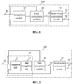
- an embodiment of the present disclosure provides a data transmission circuit 100, which includes a comparison module 10, a data conversion module 20, and a read-write conversion circuit 70.
- the comparison module 10 is configured to receive first data on a data bus 30 and second data on a global data line 40, and compare the first data with the second data to output a comparison result of whether a number of different bits between the first data and the second data exceeds a preset threshold, where the first data and the second data have a same preset bit width.
- the data conversion module 20 is electrically connected to the data bus 30, the comparison module 10 and the global data line 40, and is configured to: in a case that the comparison result indicates that the number of different bits exceeds the preset threshold, invert the first data and transmit the inverted first data to the global data line 40; and in a case that the comparison result indicates that the number of different bits does not exceed the preset threshold, transmit the first data to the global data line 40.
- the read-write conversion circuit 70 is electrically connected to the global data line 40, a local data line 81 and a complementary local data line 82, and is configured to: in a case that the comparison result indicates that the number of different bits exceeds the preset threshold, transmit data on the global data line 40 to the complementary local data line 82; and in a case that the comparison result indicates that the number of different bits does not exceed the preset threshold, transmit data on the global data line 40 to the local data line 81.
- the local data line 81 transmits a signal having a phase which is opposite to a phase of a signal transmitted by the complementary local data line 82.
- the comparison module 10 is configured to receive the first data on the data bus 30 and the second data on the global data line 40, and compare the first data with the second data to output the comparison result of whether the number of different bits between the first data and the second data exceeds the preset threshold, where the first data and the second data have the same preset bit width, so that the data conversion module 20 inverts the first data and transmits the inverted first data to the global data line 40 in a case that the comparison result indicates that the number of different bits exceeds the preset threshold, and transmits the first data to the global data line 40 in a case that the comparison result indicates that the number of different bits does not exceed the preset threshold.
- the number of inversions of the data during the data transmission through the data bus 30, the global data line 40 and the local data line 81, or through the data bus 30, the global data line 40 and the complementary local data line 82 are reduced, so as to effectively reduce the power consumption during the data transmission through the data bus 30, the global data line 40 and the local data line 81, or through the data bus 30, the global data line 40 and the complementary local data line 82.
- the energy consumption of the semiconductor storage apparatus 200 is reduced in a case of ensuring that the density and number of the storage cells in the storage cell array are not reduced. Since the data transmitted by the local data line 81 and the complementary local data line 82 can be used as references to each other, the accuracy of data transmission to the rear-stage circuit is improved while the efficiency of the data transmission is ensured.
- the data bus 30 in the embodiments of the present disclosure is intended to schematically illustrate a front-stage data line of the global data line 40 in the process of writing data into the semiconductor storage apparatus, and is not used as the limitation to the present disclosure.
- the read-write conversion circuit 70 is configured to: pull down the local data line 81 to a low level when the global data line 40 is at a high level in a case that the comparison result indicates that the number of different bits exceeds the preset threshold; and pull down the complementary local data line 82 to the low level when the global data line 40 is at the high level in a case that the comparison result indicates that the number of different bits does not exceed the preset threshold.
- the read-write conversion circuit 70 is configured to: pull down the local data line 81 to the low level when the global data line 40 is at the high level in a case that the comparison result output by the comparison module 10 indicates that the number of different bits exceeds the preset threshold; and pull down the complementary local data line 82 to the low level when the global data line 40 is at the high level in a case that the comparison result indicates that the number of different bits does not exceed the preset threshold.
- the read-write conversion circuit 70 it is convenient for the read-write conversion circuit 70 to transmit the data on the global data line 40 to the complementary local data line 82 in a case that the comparison result indicates that the number of different bits exceeds the preset threshold, and transmit the data on the global data line 40 to the local data line 81 in a case that the comparison result indicates that the number of different bits does not exceed the preset threshold, so that the data on the data bus 30 can be accurately transmitted to the local data line 81 or the complementary local data line 82 and the number of inversions of the data during the data transmission can be reduced, so as to effectively reduce the power consumption during the data transmission through the data bus 30, the global data line 40 and the local data line 81, or through the data bus 30, the global data line 40 and the complementary local data line 82.
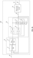
- the preset threshold is half of the preset bit width; and the comparison module 10 includes a comparison unit 11 and a state recognition unit 12.
- the comparison unit 11 is configured to compare the first data with the second data bit by bit and output comparison state data of respective bits.
- the state recognition unit 12 is electrically connected to the comparison unit 11 and is configured to perform statistics on the comparison state data of the respective bits and output the comparison result according to a statistical result.
- the number of inversions of the data is reduced under the premise that the accuracy of the data transmission is ensured, so as to effectively reduce the power consumption during the data transmission.
- the data conversion module 20 includes a first transmission unit 21, a first inverter unit 22, a second transmission unit 23, and a second inverter unit 24.
- the first transmission unit 21 is electrically connected to the data bus 30 and the global data line 40 and is electrically connected to an output terminal of the state recognition unit 12 through the first inverter unit 22, and is configured to transmit the first data to the global data line 40 in a case that the comparison result output by the comparison module 10 indicates that the number of different bits does not exceed the preset threshold.
- the second transmission unit 23 is electrically connected to the global data line 40 and the output terminal of the state recognition unit 12 and is electrically connected to the data bus 30 through the second inverter unit 24, and is configured to invert the first data and transmit the inverted first data to the global data line 40 in a case that the comparison result output by the comparison module 10 indicates that the number of different bits exceeds the preset threshold.
- the data conversion module 20 is electrically connected to the read-write conversion circuit 70 through a data bus buffer module 50.
- the data bus buffer module 50 is further electrically connected to the state recognition unit 12 and is configured to generate a data polarity identification signal according to the comparison result.
- the data bus buffer module 50 includes a write unit 51; and the write unit 51 is configured to transmit the first data to the global data line 40, or invert the first data and transmit the inverted first data to the global data line 40.
- the number of inversions of the data is reduced under the premise that the accuracy of the data transmission is ensured, so as to effectively reduce the power consumption in the process of writing the data into the global data line 40 through the data bus 30.
- the read-write conversion circuit 70 includes a write enable module 71 and a write drive circuit 72.
- the write enable module 71 is configured to generate a write enable signal WrEn and an inverted write enable signal WrEn_ according to the data polarity identification signal pl and an initial write enable signal we.
- the write drive circuit 72 is configured to generate third data according to the write enable signal WrEn, the inverted write enable signal WrEn_ and the second data, and transmit the third data to the local data line 81 or the complementary local data line 82, to ensure the accuracy of the data transmission.
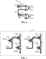
- the write enable module 71 includes a first inverter Inv1, a first NOR gate Nor1, a second inverter Inv2, and a second NOR gate Nor2.
- the first inverter Inv1 has an input terminal configured to be electrically connected to the initial write enable signal we, and an output terminal configured to output a first inverted write enable signal We1_.
- the first NOR gate Nor1 has input terminals configured to be electrically connected to the data polarity identification signal pl and the output terminal of the first inverter Inv1, and an output terminal configured to output the write enable signal WrEn.
- the second inverter Inv2 has an input terminal configured to be electrically connected to the data polarity identification signal pl, and an output terminal configured to output an inverted data polarity identification signal Pl_.
- the second NOR gate Nor2 has input terminals configured to be electrically connected to the output terminal of the second inverter Inv2 and the output terminal of the first inverter Inv1, and an output terminal configured to output the inverted write enable signal WrEn_.
- the write drive circuit 72 can be controlled, according to the write enable signal WrEn and the inverted write enable signal WrEn_, to generate the third data according to the data on the global data line 40 and transmit the third data to the local data line LIO or the complementary local data line LIO_, so as to implement the recovery of the transmission data, and ensure the accuracy of the data transmission.
- the write drive circuit 72 includes a first switch unit 721, a second switch unit 722, a third switch unit 723, a fourth switch unit 724, a fifth switch unit 725, and a sixth switch unit 726.
- the first switch unit 721 is configured to be electrically connected to the complementary local data line LIO_ and the global data line YIO according to the inverted write enable signal WrEn_.
- the second switch unit 722 has a control terminal configured to be electrically connected to the global data line YIO, a first terminal configured to be electrically connected to the local data line LIO, and a second terminal configured to be electrically connected to a first node a.
- the third switch unit 723 is configured to be electrically connected to the first node a and a ground according to the inverted write enable signal WrEn_.
- the fourth switch unit 724 is configured to be electrically connected to the local data line LIO and the global data line YIO according to the write enable signal WrEn.
- the fifth switch unit 725 has a control terminal configured to be electrically connected to the global data line YIO, a first terminal configured to be electrically connected to the complementary local data line LIO_, and a second terminal configured to be electrically connected to a second node b.
- the sixth switch unit 726 is configured to be electrically connected to the second node b and the ground according to the write enable signal WrEn.
- the power consumption in the process of writing the data into the local data line LIO or the complementary local data line LIO_ through the data bus Data bus and the global data line YIO is effectively reduced by reducing the number of inversions of the written data in the transmission process, and in particular, the inversions of the data on the global data line YIO are reduced.
- the data conversion module 20 is further configured to invert the second data and transmit the inverted second data to the data bus 30 in a case that the comparison result output by the comparison module 10 indicates that the number of different bits exceeds the preset threshold (e.g., half of the preset bit width), and is further configured to transmit the second data to the data bus 30 in a case that the comparison result indicates that the number of different bits does not exceed the preset threshold.
- the preset threshold e.g., half of the preset bit width
- the data conversion module 20 inverts the second data provided by the global data line 40 and transmit the inverted second data to the data bus 30; and in a case that the comparison result output by the comparison module 10 indicates that the number of different bits does not exceed the preset threshold, the data conversion module 20 transmits the second data provided by the global data line 40 to the data bus 30, so as to effectively reduce the power consumption in the process of transmitting the read data to the data bus 30 through the global data line 40.
- the preset threshold e.g., half of the preset bit width
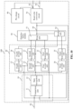
- the data conversion module 20 further includes a third transmission unit 25, a third inverter unit 26, a fourth transmission unit 27, and a fourth inverter unit 28.
- the third transmission unit 25 is electrically connected to the data bus 30 and the global data line 40 and is electrically connected to an output terminal of the comparison module 10 through the third inverter unit 26, and is configured to transmit the second data to the data bus 30 in a case that the comparison result output by the comparison module 10 indicates that the number of different bits does not exceed the preset threshold.
- the fourth transmission unit 27 is electrically connected to the data bus 30 and the output terminal of the comparison module 10 and is electrically connected to the global data line 40 through the fourth inverter unit 28, and is configured to invert the second data and transmit the inverted second data to the data bus 30 in a case that the comparison result output by the comparison module 10 indicates that the number of different bits exceeds the preset threshold.
- the data on the global data line can be accurately transmitted to the data bus, and the number of inversions of the data during the data transmission can be reduced, so as to effectively reduce the power consumption during transmission of the data through the global data line and the data bus in the process of reading the data.
- the data bus buffer module 50 further includes a read unit 52.
- the read unit 52 is configured to transmit the second data to the third transmission unit 25, or invert the second data through the fourth inverter unit 28 and transmit the inverted second data to the fourth transmission unit 27.
- the fourth transmission unit 27 inverts the second data provided by the global data line YIO and transmit the inverted second data to the data bus 30; and in a case that the comparison result output by the comparison module 10 indicates that the number of different bits does not exceed the preset threshold, the third transmission unit 25 transmits the second data provided by the global data line 40 to the data bus 30.
- This embodiment can effectively reduce the power consumption in the process of transmitting the read data to the data bus 30 through the global data line 40.
- an embodiment of the present disclosure provides a storage apparatus 200.
- the storage apparatus 200 includes the data transmission circuit 100 of any one of the aforementioned embodiments of the present disclosure, and configured to store and transmit data during a read operation or a write operation.
- an embodiment of the present disclosure provides a data transmission method.
- the method includes the following operations.
- first data on a data bus is compared with second data on a global data line, and a comparison result of whether a number of different bits between the first data and the second data exceeds a preset threshold is output, where the first data and the second data have a same preset bit width.
- the first data is inverted and the inverted first data is transmitted to the global data line; if the comparison result indicates that the number of different bits does not exceed the preset threshold, the first data is transmitted to the global data line.
- the local data line transmits a signal having a phase which is opposite to a phase of a signal transmitted by the complementary local data line.
- the first data on the data bus is compared with the second data on the global data line and the comparison result of whether the number of different bits between the first data and the second data exceeds the preset threshold is output, where the first data and the second data have the same preset bit width.
- the comparison result indicates that the number of different bits exceeds the preset threshold
- the first data is inverted and the inverted first data is transmitted to the global data line; in a case that the comparison result indicates that the number of different bits does not exceed the preset threshold, the first data is transmitted to the global data line.
- the second data is inverted and the inverted second data is transmitted to the data bus; in a case that the comparison result indicates that the number of different bits does not exceed the preset threshold, the second data is transmitted to the data bus.
- the transmitted data generally includes a data string consisting of 0 and 1
- the number of inversions of the data is reduce to effectively reduce the power consumption during the transmission of the data through the data bus, the global data line and the local data line, or through the data bus, the global data line and the complementary local data line. Therefore, the energy consumption of the semiconductor storage apparatus is reduced in a case of ensuring that the density and number of the storage cells in the storage cell array are not reduced. Since the data transmitted by the local data line and the complementary local data line can be used as references to each other, the accuracy of data transmission to the rear-stage circuit is improved while ensuring the efficiency of the data transmission.
- the method includes the following operations.
- first data on a data bus is compared with second data on a global data line, and a comparison result of whether a number of different bits between the first data and the second data exceeds a preset threshold is output, where the first data and the second data have a same preset bit width.
- the first data is inverted and the inverted first data is transmitted to the global data line; if the comparison result indicates that the number of different bits does not exceed the preset threshold, the first data is transmitted to the global data line, where the preset threshold is half of the preset bit width.
- the second data is inverted and the inverted second data is transmitted to the data bus; if the comparison result indicates that the number of different bits does not exceed the preset threshold, the second data is transmitted to the data bus.
- the second transmission unit 23 inverts the first data and transmit the inverted first data to the global data line 40; and in a case that the comparison result output by the comparison module 10 indicates that the number of different bits does not exceed the preset threshold, the first transmission unit 21 transmits the first data to the global data line 40, so as to effectively reduce the power consumption in the process of transmitting the written data to the global data line 40 through the data bus 30.
- the preset threshold e.g., half of the preset bit width
- the fourth transmission unit 27 inverts the second data provided by the global data line 40 and transmit the inverted second data to the data bus 30; and in a case that the comparison result output by the comparison module 10 indicates that the number of different bits does not exceed the preset threshold, the third transmission unit 25 transmits the second data provided by the global data line 40 to the data bus 30.
- This embodiment can effectively reduce the power consumption in the process of transmitting the read data to the data bus 30 through the global data line 40.
- An embodiment of the present disclosure provides a computer-readable storage medium, having a computer program stored thereon that, when executed by a processor, cause the processor to perform the data transmission method of any one of the embodiments of the present disclosure.
- FIG. 12 and FIG. 13 are displayed in sequence according to arrows, the operations are not necessarily performed in the sequence indicated by the arrows. Unless otherwise explicitly specified in the present disclosure, execution of the operations is not strictly limited, and the operations may be performed in other sequences. Moreover, at least a part of the operations in FIG. 12 and FIG. 13 may include a plurality of operations or a plurality of stages. These operations or stages are not necessarily completed at the same moment, but may be performed at different moments. The execution sequence of these operations or stages may not be necessarily performed sequentially, but may be performed in turn or alternately with other operations or at least a part of operations or stages among other operations.
- the non-volatile memory may include a read-only memory (ROM), a programmable ROM (PROM), an electrically programmable ROM (EPROM), an electrically erasable programmable ROM (EEPROM), or a flash memory.
- ROM read-only memory
- PROM programmable ROM
- EPROM electrically programmable ROM
- EEPROM electrically erasable programmable ROM
- the volatile memory may include a random access memory (RAM) or an external cache.
- the RAM may be obtained in a plurality of forms, such as a static RAM (SRAM), a dynamic RAM (DRAM), a synchronous DRAM (SDRAM), a double data rate SDRAM (DDRSDRAM), an enhanced SDRAM (ESDRAM), a Synchlink DRAM (SLDRAM), a direct Rambus dynamic RAM (DRDRAM), and a Rambus dynamic RAM (RDRAM).
- SRAM static RAM
- DRAM dynamic RAM
- SDRAM synchronous DRAM
- DDRSDRAM double data rate SDRAM
- ESDRAM enhanced SDRAM
- SLDRAM Synchlink DRAM
- DRAM direct Rambus dynamic RAM
- RDRAM Rambus dynamic RAM
Landscapes
- Engineering & Computer Science (AREA)
- Theoretical Computer Science (AREA)
- Human Computer Interaction (AREA)
- Physics & Mathematics (AREA)
- General Engineering & Computer Science (AREA)
- General Physics & Mathematics (AREA)
- Microelectronics & Electronic Packaging (AREA)
- Computer Hardware Design (AREA)
- Dc Digital Transmission (AREA)
Abstract
Description
- This application claims priority to
Chinese patent application No. 202110328177.4 filed on March 26, 2021 - The present disclosure relates to the field of semiconductor storage technologies, and in particular, to a data transmission circuit and method, and a storage apparatus.
- With rapid developments of semiconductor technologies, the market has more and more requirements for the storage capability and power saving performance of a semiconductor storage apparatus, which imposes higher requirements on the power saving performances of an external circuit region and a storage array region of a control circuit for controlling read and write in the semiconductor storage apparatus.
- However, due to the increasing of the density and number of storage cells in an storage cell array, in the process of writing data into the semiconductor storage apparatus, when data is written into a data bus through a data terminal and is transmitted to a rear-stage data line, the length of the data transmission path through which the data passes is increased, which results in that the power consumption is increased and the data transmission rate is reduced in the process of transmitting the written data to a local data line through the data terminal.
- If the energy consumption in the process of transmitting the written data to the local data line through the data terminal can be reduced in a case of ensuring that the density and number of the storage cells in the storage cell array are not reduced, this will increase the possibility of further improving the storage capability of the semiconductor storage apparatus and reducing the energy consumption of the semiconductor storage apparatus.
- In a first aspect of the present disclosure, a data transmission circuit is provided. The data transmission circuit includes a comparison module, a data conversion module, and a read-write conversion circuit. The comparison module is configured to receive first data on a data bus and second data on a global data line, and compare the first data with the second data to output a comparison result of whether a number of different bits between the first data and the second data exceeds a preset threshold, where the first data and the second data have a same preset bit width. The data conversion module is electrically connected to the data bus, the comparison module and the global data line, and is configured to: invert the first data and transmit the inverted first data to the global data line in response to the comparison result indicating that the number of different bits exceeds the preset threshold, and transmit the first data to the global data line in response to the comparison result indicating that the number of different bits does not exceed the preset threshold. The read-write conversion circuit is electrically connected to the global data line, a local data line and a complementary local data line, and is configured to: transmit data on the global data line to the complementary local data line in response to the comparison result indicating that the number of different bits exceeds the preset threshold, and transmit data on the global data line to the local data line in response to the comparison result indicating that the number of different bits does not exceed the preset threshold.
- In a second aspect of the present disclosure, a storage apparatus is provided. The storage apparatus includes the data transmission circuit in the first aspect, and configured to store and transmit data during a read operation or a write operation.
- In a third aspect of the present disclosure, a data transmission method is provided. The data transmission method includes the following operations. First data on a data bus and second data on a global data line are compared, and a comparison result of whether a number of different bits between the first data and the second data exceeds a preset threshold is output, where the first data and the second data have a same preset bit width. In response to the comparison result indicating that the number of different bits exceeds the preset threshold, the first data is inverted and the inverted first data is transmitted to the global data line; and in response to the comparison result indicating that the number of different bits does not exceed the preset threshold, the first data is transmitted to the global data line. In response to the comparison result indicating that the number of different bits exceeds the preset threshold, data on the global data line is transmitted to a complementary local data line; and in response to the comparison result indicating that the number of different bits does not exceed the preset threshold, data on the global data line is transmitted to a local data line, where the local data line transmits a signal having a phase which is opposite to a phase of a signal transmitted by the complementary local data line.
- Details of various embodiments of the present disclosure are provided in the accompanying drawings and descriptions below. According to the recitations of the description, accompanying drawings and claims, a person skilled in the art would readily understand other features, a solved problem and a technical effect of the present disclosure.
- To explain the technical solutions in the embodiments of the present disclosure or the related techniques more clearly, the accompanying drawings required to be used in the descriptions of the embodiments or the related techniques are simply introduced below. Apparently, the accompanying drawings in the descriptions below are merely some embodiments of the present disclosure. To better describe and explain the embodiments of the present disclosure, references are made to one or more drawings. However, additional details or examples for describing the accompanying drawings should not be considered as the limitation to the scope of any one of the invention creation of the present disclosure, currently described embodiments or preferable modes.
-
FIG. 1 is a schematic diagram of a principle of a data transmission circuit provided by a first embodiment of the present disclosure. -
FIG. 2 is a schematic diagram of a principle of a data transmission circuit provided by a second embodiment of the present disclosure. -
FIG. 3a is a schematic diagram of a principle of a data transmission circuit provided by a third embodiment of the present disclosure. -
FIG. 3b is a schematic diagram of an implementation ofFIG. 3a . -
FIG. 4 is a schematic diagram of a principle of a data transmission circuit provided by a fourth embodiment of the present disclosure. -
FIG. 5 is a schematic diagram of a principle of a data transmission circuit provided by a fifth embodiment of the present disclosure. -
FIG. 6 is a schematic circuit diagram of a write enable module in a data transmission circuit provided by an embodiment of the present disclosure. -
FIG. 7 is a schematic circuit diagram of a write drive circuit in a data transmission circuit provided by an embodiment of the present disclosure. -
FIG. 8a is a schematic diagram of a principle of a data transmission circuit provided by a sixth embodiment of the present disclosure. -
FIG. 8b is a schematic diagram of an implementation ofFIG. 8a . -
FIG. 9 is a schematic diagram of a principle of a data transmission circuit provided by a seventh embodiment of the present disclosure. -
FIG. 10 is a schematic diagram of a principle of a data transmission circuit provided by an eighth embodiment of the present disclosure. -
FIG. 11 is a structural block of a storage apparatus provided by an embodiment of the present disclosure. -
FIG. 12 is a flowchart of a data transmission method provided by an embodiment of the present disclosure. -
FIG. 13 is a flowchart of a data transmission method provided by another embodiment of the present disclosure. - To facilitate the understanding of the present disclosure, the present disclosure would be described more comprehensively with reference to the related accompanying drawings. The preferred embodiments of the present disclosure are provided in the accompanying drawings. However, the present disclosure can be implemented through many different forms, which are not limited in the embodiments described herein. On the contrary, the purpose for providing the embodiments is to make the disclosed contents of the present disclosure more thorough and comprehensive.
- Unless otherwise defined, all techniques and scientific terms used herein have the same meanings as those generally understood by a person skilled in the technical field of the present disclosure. The terms used in the description of the present disclosure are only used for the purpose of describing specific embodiments, rather than the purpose of limiting the present disclosure. In addition, some terms used through the description and the accompanying claims refer to specific components. A person skilled in the art would understand that a manufacturer may use different names for indicating a component. The present disclosure does not intend to distinguish components with different names but the same function. In the following descriptions and embodiments, terms "comprising" and "including" are both used in an open type, and therefore, should be interpreted as "comprising, but not limited to...". Similarly, the term "connecting" desires to express an indirect or direct electrical connection. Accordingly, if a device is connected to another device, connection may be completed through the direction electrical connection, or may be completed through the indirect electrical connection between other devices and a connection member.
- It should be understood that the terms "first", "second" and the like may be used for describing various components herein. However, these components should not be limited by these terms. These terms are merely used for distinguishing one component from another component. For example, without departing from the scope of the present disclosure, a first component may be referred to as a second component, and similarly, the second component may be referred to as the first component.
- With reference to
FIG. 1 , an embodiment of the present disclosure provides adata transmission circuit 100, which includes acomparison module 10, adata conversion module 20, and a read-write conversion circuit 70. Thecomparison module 10 is configured to receive first data on adata bus 30 and second data on aglobal data line 40, and compare the first data with the second data to output a comparison result of whether a number of different bits between the first data and the second data exceeds a preset threshold, where the first data and the second data have a same preset bit width. Thedata conversion module 20 is electrically connected to thedata bus 30, thecomparison module 10 and theglobal data line 40, and is configured to: in a case that the comparison result indicates that the number of different bits exceeds the preset threshold, invert the first data and transmit the inverted first data to theglobal data line 40; and in a case that the comparison result indicates that the number of different bits does not exceed the preset threshold, transmit the first data to theglobal data line 40. The read-write conversion circuit 70 is electrically connected to theglobal data line 40, alocal data line 81 and a complementarylocal data line 82, and is configured to: in a case that the comparison result indicates that the number of different bits exceeds the preset threshold, transmit data on theglobal data line 40 to the complementarylocal data line 82; and in a case that the comparison result indicates that the number of different bits does not exceed the preset threshold, transmit data on theglobal data line 40 to thelocal data line 81. - In an embodiment, the
local data line 81 transmits a signal having a phase which is opposite to a phase of a signal transmitted by the complementarylocal data line 82. - As an example, with continued reference to
FIG. 1 , thecomparison module 10 is configured to receive the first data on thedata bus 30 and the second data on theglobal data line 40, and compare the first data with the second data to output the comparison result of whether the number of different bits between the first data and the second data exceeds the preset threshold, where the first data and the second data have the same preset bit width, so that thedata conversion module 20 inverts the first data and transmits the inverted first data to theglobal data line 40 in a case that the comparison result indicates that the number of different bits exceeds the preset threshold, and transmits the first data to theglobal data line 40 in a case that the comparison result indicates that the number of different bits does not exceed the preset threshold. Under the premise that the accuracy of the data transmission is ensured, the number of inversions of the data during the data transmission through thedata bus 30, theglobal data line 40 and thelocal data line 81, or through thedata bus 30, theglobal data line 40 and the complementarylocal data line 82 are reduced, so as to effectively reduce the power consumption during the data transmission through thedata bus 30, theglobal data line 40 and thelocal data line 81, or through thedata bus 30, theglobal data line 40 and the complementarylocal data line 82. Thus, the energy consumption of thesemiconductor storage apparatus 200 is reduced in a case of ensuring that the density and number of the storage cells in the storage cell array are not reduced. Since the data transmitted by thelocal data line 81 and the complementarylocal data line 82 can be used as references to each other, the accuracy of data transmission to the rear-stage circuit is improved while the efficiency of the data transmission is ensured. - It should be noted that the
data bus 30 in the embodiments of the present disclosure is intended to schematically illustrate a front-stage data line of theglobal data line 40 in the process of writing data into the semiconductor storage apparatus, and is not used as the limitation to the present disclosure. - Furthermore, with continued reference to
FIG. 1 , in an embodiment of the present disclosure, the read-write conversion circuit 70 is configured to: pull down thelocal data line 81 to a low level when theglobal data line 40 is at a high level in a case that the comparison result indicates that the number of different bits exceeds the preset threshold; and pull down the complementarylocal data line 82 to the low level when theglobal data line 40 is at the high level in a case that the comparison result indicates that the number of different bits does not exceed the preset threshold. - As an example, with continued reference to
FIG. 1 , the read-write conversion circuit 70 is configured to: pull down thelocal data line 81 to the low level when theglobal data line 40 is at the high level in a case that the comparison result output by thecomparison module 10 indicates that the number of different bits exceeds the preset threshold; and pull down the complementarylocal data line 82 to the low level when theglobal data line 40 is at the high level in a case that the comparison result indicates that the number of different bits does not exceed the preset threshold. It is convenient for the read-write conversion circuit 70 to transmit the data on theglobal data line 40 to the complementarylocal data line 82 in a case that the comparison result indicates that the number of different bits exceeds the preset threshold, and transmit the data on theglobal data line 40 to thelocal data line 81 in a case that the comparison result indicates that the number of different bits does not exceed the preset threshold, so that the data on thedata bus 30 can be accurately transmitted to thelocal data line 81 or the complementarylocal data line 82 and the number of inversions of the data during the data transmission can be reduced, so as to effectively reduce the power consumption during the data transmission through thedata bus 30, theglobal data line 40 and thelocal data line 81, or through thedata bus 30, theglobal data line 40 and the complementarylocal data line 82. - Furthermore, with reference to
FIG. 2 , in an embodiment of the present disclosure, the preset threshold is half of the preset bit width; and thecomparison module 10 includes acomparison unit 11 and astate recognition unit 12. Thecomparison unit 11 is configured to compare the first data with the second data bit by bit and output comparison state data of respective bits. Thestate recognition unit 12 is electrically connected to thecomparison unit 11 and is configured to perform statistics on the comparison state data of the respective bits and output the comparison result according to a statistical result. In this embodiment, the number of inversions of the data is reduced under the premise that the accuracy of the data transmission is ensured, so as to effectively reduce the power consumption during the data transmission. - As an example, with reference to
FIG. 3a andFIG. 3b , in an embodiment of the present disclosure, thedata conversion module 20 includes afirst transmission unit 21, afirst inverter unit 22, asecond transmission unit 23, and asecond inverter unit 24. Thefirst transmission unit 21 is electrically connected to thedata bus 30 and theglobal data line 40 and is electrically connected to an output terminal of thestate recognition unit 12 through thefirst inverter unit 22, and is configured to transmit the first data to theglobal data line 40 in a case that the comparison result output by thecomparison module 10 indicates that the number of different bits does not exceed the preset threshold. Thesecond transmission unit 23 is electrically connected to theglobal data line 40 and the output terminal of thestate recognition unit 12 and is electrically connected to thedata bus 30 through thesecond inverter unit 24, and is configured to invert the first data and transmit the inverted first data to theglobal data line 40 in a case that the comparison result output by thecomparison module 10 indicates that the number of different bits exceeds the preset threshold. - Furthermore, with reference to
FIG. 4 , in an embodiment of the present disclosure, thedata conversion module 20 is electrically connected to the read-write conversion circuit 70 through a databus buffer module 50. The databus buffer module 50 is further electrically connected to thestate recognition unit 12 and is configured to generate a data polarity identification signal according to the comparison result. The databus buffer module 50 includes awrite unit 51; and thewrite unit 51 is configured to transmit the first data to theglobal data line 40, or invert the first data and transmit the inverted first data to theglobal data line 40. The number of inversions of the data is reduced under the premise that the accuracy of the data transmission is ensured, so as to effectively reduce the power consumption in the process of writing the data into theglobal data line 40 through thedata bus 30. - Furthermore, with reference to
FIG. 5 , in an embodiment of the present disclosure, the read-write conversion circuit 70 includes a write enablemodule 71 and awrite drive circuit 72. The write enablemodule 71 is configured to generate a write enable signal WrEn and an inverted write enable signal WrEn_ according to the data polarity identification signal pl and an initial write enable signal we. Thewrite drive circuit 72 is configured to generate third data according to the write enable signal WrEn, the inverted write enable signal WrEn_ and the second data, and transmit the third data to thelocal data line 81 or the complementarylocal data line 82, to ensure the accuracy of the data transmission. - Furthermore, with reference to
FIG. 6 , in an embodiment of the present disclosure, the write enablemodule 71 includes a first inverter Inv1, a first NOR gate Nor1, a second inverter Inv2, and a second NOR gate Nor2. The first inverter Inv1 has an input terminal configured to be electrically connected to the initial write enable signal we, and an output terminal configured to output a first inverted write enable signal We1_. The first NOR gate Nor1 has input terminals configured to be electrically connected to the data polarity identification signal pl and the output terminal of the first inverter Inv1, and an output terminal configured to output the write enable signal WrEn. The second inverter Inv2 has an input terminal configured to be electrically connected to the data polarity identification signal pl, and an output terminal configured to output an inverted data polarity identification signal Pl_. The second NOR gate Nor2 has input terminals configured to be electrically connected to the output terminal of the second inverter Inv2 and the output terminal of the first inverter Inv1, and an output terminal configured to output the inverted write enable signal WrEn_. Therefore, thewrite drive circuit 72 can be controlled, according to the write enable signal WrEn and the inverted write enable signal WrEn_, to generate the third data according to the data on theglobal data line 40 and transmit the third data to the local data line LIO or the complementary local data line LIO_, so as to implement the recovery of the transmission data, and ensure the accuracy of the data transmission. - Furthermore, with reference to
FIG. 7 , in an embodiment of the present disclosure, thewrite drive circuit 72 includes afirst switch unit 721, asecond switch unit 722, athird switch unit 723, afourth switch unit 724, afifth switch unit 725, and asixth switch unit 726. Thefirst switch unit 721 is configured to be electrically connected to the complementary local data line LIO_ and the global data line YIO according to the inverted write enable signal WrEn_. Thesecond switch unit 722 has a control terminal configured to be electrically connected to the global data line YIO, a first terminal configured to be electrically connected to the local data line LIO, and a second terminal configured to be electrically connected to a first node a. Thethird switch unit 723 is configured to be electrically connected to the first node a and a ground according to the inverted write enable signal WrEn_. Thefourth switch unit 724 is configured to be electrically connected to the local data line LIO and the global data line YIO according to the write enable signal WrEn. Thefifth switch unit 725 has a control terminal configured to be electrically connected to the global data line YIO, a first terminal configured to be electrically connected to the complementary local data line LIO_, and a second terminal configured to be electrically connected to a second node b. Thesixth switch unit 726 is configured to be electrically connected to the second node b and the ground according to the write enable signal WrEn. In this embodiment, the power consumption in the process of writing the data into the local data line LIO or the complementary local data line LIO_ through the data bus Data bus and the global data line YIO is effectively reduced by reducing the number of inversions of the written data in the transmission process, and in particular, the inversions of the data on the global data line YIO are reduced. - Furthermore, with reference to
FIG. 8a andFIG. 8b , in an embodiment of the present disclosure, thedata conversion module 20 is further configured to invert the second data and transmit the inverted second data to thedata bus 30 in a case that the comparison result output by thecomparison module 10 indicates that the number of different bits exceeds the preset threshold (e.g., half of the preset bit width), and is further configured to transmit the second data to thedata bus 30 in a case that the comparison result indicates that the number of different bits does not exceed the preset threshold. For example, during the data reading, in a case that the comparison result output by thecomparison module 10 indicates that the number of different bits exceeds the preset threshold (e.g., half of the preset bit width), thedata conversion module 20 inverts the second data provided by theglobal data line 40 and transmit the inverted second data to thedata bus 30; and in a case that the comparison result output by thecomparison module 10 indicates that the number of different bits does not exceed the preset threshold, thedata conversion module 20 transmits the second data provided by theglobal data line 40 to thedata bus 30, so as to effectively reduce the power consumption in the process of transmitting the read data to thedata bus 30 through theglobal data line 40. - Furthermore, with reference to
FIG. 9 , in an embodiment of the present disclosure, thedata conversion module 20 further includes athird transmission unit 25, athird inverter unit 26, afourth transmission unit 27, and afourth inverter unit 28. Thethird transmission unit 25 is electrically connected to thedata bus 30 and theglobal data line 40 and is electrically connected to an output terminal of thecomparison module 10 through thethird inverter unit 26, and is configured to transmit the second data to thedata bus 30 in a case that the comparison result output by thecomparison module 10 indicates that the number of different bits does not exceed the preset threshold. Thefourth transmission unit 27 is electrically connected to thedata bus 30 and the output terminal of thecomparison module 10 and is electrically connected to theglobal data line 40 through thefourth inverter unit 28, and is configured to invert the second data and transmit the inverted second data to thedata bus 30 in a case that the comparison result output by thecomparison module 10 indicates that the number of different bits exceeds the preset threshold. In this embodiment, the data on the global data line can be accurately transmitted to the data bus, and the number of inversions of the data during the data transmission can be reduced, so as to effectively reduce the power consumption during transmission of the data through the global data line and the data bus in the process of reading the data. - Furthermore, with reference to
FIG. 10 , in an embodiment of the present disclosure, the databus buffer module 50 further includes aread unit 52. Theread unit 52 is configured to transmit the second data to thethird transmission unit 25, or invert the second data through thefourth inverter unit 28 and transmit the inverted second data to thefourth transmission unit 27. For example, during the data reading, in a case that the comparison result output by thecomparison module 10 indicates that the number of different bits exceeds the preset threshold (e.g., half of the preset bit width), thefourth transmission unit 27 inverts the second data provided by the global data line YIO and transmit the inverted second data to thedata bus 30; and in a case that the comparison result output by thecomparison module 10 indicates that the number of different bits does not exceed the preset threshold, thethird transmission unit 25 transmits the second data provided by theglobal data line 40 to thedata bus 30. This embodiment can effectively reduce the power consumption in the process of transmitting the read data to thedata bus 30 through theglobal data line 40. - Furthermore, with reference to
FIG. 11 , an embodiment of the present disclosure provides astorage apparatus 200. Thestorage apparatus 200 includes thedata transmission circuit 100 of any one of the aforementioned embodiments of the present disclosure, and configured to store and transmit data during a read operation or a write operation. - For specific definitions of the
storage apparatus 200 in the embodiment, the references can be made to specific definitions of thedata transmission circuit 100 in the aforementioned embodiments of the present disclosure, and the details are not repeated herein. - Furthermore, with reference to
FIG. 12 , an embodiment of the present disclosure provides a data transmission method. The method includes the following operations. - In
operation 102, first data on a data bus is compared with second data on a global data line, and a comparison result of whether a number of different bits between the first data and the second data exceeds a preset threshold is output, where the first data and the second data have a same preset bit width. - In
operation 104, if the comparison result indicates that the number of different bits exceeds the preset threshold, the first data is inverted and the inverted first data is transmitted to the global data line; if the comparison result indicates that the number of different bits does not exceed the preset threshold, the first data is transmitted to the global data line. - In
operation 106, in a case that the comparison result indicates that the number of different bits exceeds the preset threshold, data on the global data line is transmitted to a complementary local data line; and in a case that the comparison result indicates that the number of different bits does not exceed the preset threshold, data on the global data line is transmitted to a local data line. - In an embodiment, the local data line transmits a signal having a phase which is opposite to a phase of a signal transmitted by the complementary local data line.
- Specifically, with continued reference to
FIG. 12 , the first data on the data bus is compared with the second data on the global data line and the comparison result of whether the number of different bits between the first data and the second data exceeds the preset threshold is output, where the first data and the second data have the same preset bit width. In a case that the comparison result indicates that the number of different bits exceeds the preset threshold, the first data is inverted and the inverted first data is transmitted to the global data line; in a case that the comparison result indicates that the number of different bits does not exceed the preset threshold, the first data is transmitted to the global data line. In a case that the comparison result indicates that the number of different bits exceeds the preset threshold, the second data is inverted and the inverted second data is transmitted to the data bus; in a case that the comparison result indicates that the number of different bits does not exceed the preset threshold, the second data is transmitted to the data bus. Since the transmitted data generally includes a data string consisting of 0 and 1, by applying a power saving algorithm to the transmission process of the data through the data bus, the global data line and the local data line, or through the data bus, the global data line and the complementary local data line, under the premise that the accuracy of the data transmission is ensured, the number of inversions of the data is reduce to effectively reduce the power consumption during the transmission of the data through the data bus, the global data line and the local data line, or through the data bus, the global data line and the complementary local data line. Therefore, the energy consumption of the semiconductor storage apparatus is reduced in a case of ensuring that the density and number of the storage cells in the storage cell array are not reduced. Since the data transmitted by the local data line and the complementary local data line can be used as references to each other, the accuracy of data transmission to the rear-stage circuit is improved while ensuring the efficiency of the data transmission. - Furthermore, with reference to
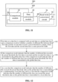
FIG. 13 , in an embodiment of the present disclosure, the method includes the following operations. - In
operation 102, first data on a data bus is compared with second data on a global data line, and a comparison result of whether a number of different bits between the first data and the second data exceeds a preset threshold is output, where the first data and the second data have a same preset bit width. - In
operation 1041, if the comparison result indicates that the number of different bits exceeds the preset threshold, the first data is inverted and the inverted first data is transmitted to the global data line; if the comparison result indicates that the number of different bits does not exceed the preset threshold, the first data is transmitted to the global data line, where the preset threshold is half of the preset bit width. - In
operation 106, in a case that the comparison result indicates that the number of different bits exceeds the preset threshold, data on the global data line is transmitted to a complementary local data line, and in a case that the comparison result indicates that the number of different bits does not exceed the preset threshold, data on the global data line is transmitted to a local data line. - In
operation 108, if the comparison result indicates that the number of different bits exceeds the preset threshold, the second data is inverted and the inverted second data is transmitted to the data bus; if the comparison result indicates that the number of different bits does not exceed the preset threshold, the second data is transmitted to the data bus. - As an example, with continued reference to
FIG. 10 andFIG. 13 , during the data writing, in a case that the comparison result output by thecomparison module 10 indicates that the number of different bits exceeds the preset threshold (e.g., half of the preset bit width), thesecond transmission unit 23 inverts the first data and transmit the inverted first data to theglobal data line 40; and in a case that the comparison result output by thecomparison module 10 indicates that the number of different bits does not exceed the preset threshold, thefirst transmission unit 21 transmits the first data to theglobal data line 40, so as to effectively reduce the power consumption in the process of transmitting the written data to theglobal data line 40 through thedata bus 30. During the data reading, in a case that the comparison result output by thecomparison module 10 indicates that the number of different bits exceeds the preset threshold, thefourth transmission unit 27 inverts the second data provided by theglobal data line 40 and transmit the inverted second data to thedata bus 30; and in a case that the comparison result output by thecomparison module 10 indicates that the number of different bits does not exceed the preset threshold, thethird transmission unit 25 transmits the second data provided by theglobal data line 40 to thedata bus 30. This embodiment can effectively reduce the power consumption in the process of transmitting the read data to thedata bus 30 through theglobal data line 40. - An embodiment of the present disclosure provides a computer-readable storage medium, having a computer program stored thereon that, when executed by a processor, cause the processor to perform the data transmission method of any one of the embodiments of the present disclosure.
- It is to be understood that although the operations in the flowcharts in
FIG. 12 andFIG. 13 are displayed in sequence according to arrows, the operations are not necessarily performed in the sequence indicated by the arrows. Unless otherwise explicitly specified in the present disclosure, execution of the operations is not strictly limited, and the operations may be performed in other sequences. Moreover, at least a part of the operations inFIG. 12 andFIG. 13 may include a plurality of operations or a plurality of stages. These operations or stages are not necessarily completed at the same moment, but may be performed at different moments. The execution sequence of these operations or stages may not be necessarily performed sequentially, but may be performed in turn or alternately with other operations or at least a part of operations or stages among other operations. - A person of ordinary skill in the art may understand that all or some of the procedures of the methods in the foregoing embodiments may be implemented by computer programs instructing relevant hardware. The computer programs may be stored in a non-transitory computer-readable storage medium. When the computer programs are executed, the procedures of the embodiments of the foregoing methods may be included. References to the memory, the storage, the database, or other media used in the embodiments provided in the present disclosure may all include a non-volatile or a volatile memory. The non-volatile memory may include a read-only memory (ROM), a programmable ROM (PROM), an electrically programmable ROM (EPROM), an electrically erasable programmable ROM (EEPROM), or a flash memory. The volatile memory may include a random access memory (RAM) or an external cache. By way of description rather than limitation, the RAM may be obtained in a plurality of forms, such as a static RAM (SRAM), a dynamic RAM (DRAM), a synchronous DRAM (SDRAM), a double data rate SDRAM (DDRSDRAM), an enhanced SDRAM (ESDRAM), a Synchlink DRAM (SLDRAM), a direct Rambus dynamic RAM (DRDRAM), and a Rambus dynamic RAM (RDRAM).
- It is noted that the foregoing embodiments are merely used for the purpose of explanations without the meaning of limiting the present disclosure.
- The technical features in the foregoing embodiments may be randomly combined. For concise description, not all possible combinations of the technical features in the embodiments are described. However, provided that combinations of the technical features do not conflict with each other, the combinations of the technical features are considered as falling within the scope described in the present disclosure.
- The foregoing embodiments show only several implementations of the present disclosure and are described in detail, which, however, are not to be construed as a limitation to the patent scope of the present disclosure. For a person of ordinary skill in the art, several transformations and improvements can be made without departing from the idea of the present disclosure. These transformations and improvements belong to the protection scope of the present disclosure. Therefore, the protection scope of the present disclosure shall be subject to the appended claims.
Claims (15)
- A data transmission circuit, comprising:a comparison module, configured to receive first data on a data bus and second data on a global data line, and compare the first data with the second data to output a comparison result of whether a number of different bits between the first data and the second data exceeds a preset threshold, wherein the first data and the second data have a same preset bit width;a data conversion module, electrically connected to the data bus, the comparison module and the global data line, and configured to: invert the first data and transmit the inverted first data to the global data line in response to the comparison result indicating that the number of different bits exceeds the preset threshold, and transmit the first data to the global data line in response to the comparison result indicating that the number of different bits does not exceed the preset threshold; anda read-write conversion circuit, electrically connected to the global data line, a local data line and a complementary local data line, and configured to: transmit data on the global data line to the complementary local data line in response to the comparison result indicating that the number of different bits exceeds the preset threshold, and transmit data on the global data line to the local data line in response to the comparison result indicating that the number of different bits does not exceed the preset threshold.
- The data transmission circuit of claim 1, wherein the read-write conversion circuit is configured to:in response to the comparison result indicating that the number of different bits exceeds the preset threshold, pull down the local data line to a low level when the global data line is at a high level; andin response to the comparison result indicating that the number of different bits does not exceed the preset threshold, pull down the complementary local data line to the low level when the global data line is at the high level.
- The data transmission circuit of claim 1, wherein the preset threshold is half of the preset bit width; and the comparison module comprises:a comparison unit, configured to compare the first data with the second data bit by bit and output comparison state data of respective bits; anda state recognition unit, electrically connected to the comparison unit, and configured to perform statistics on the comparison state data of the respective bits and output the comparison result according to a statistical result.
- The data transmission circuit of claim 3, wherein the data conversion module comprises:a first transmission unit, electrically connected to the data bus and the global data line and electrically connected to an output terminal of the state recognition unit through a first inverter unit, and configured to transmit the first data to the global data line in response to the comparison result indicating that the number of different bits does not exceed the preset threshold; anda second transmission unit, electrically connected to the global data line and the output terminal of the state recognition unit and electrically connected to the data bus through a second inverter unit, and configured to invert the first data and transmit the inverted first data to the global data line in response to the comparison result indicating that the number of different bits exceeds the preset threshold.
- The data transmission circuit of claim 4, wherein the data conversion module is electrically connected to the read-write conversion circuit through a data bus buffer module; andthe data bus buffer module is further electrically connected to the state recognition unit, and configured to generate a data polarity identification signal according to the comparison result;wherein the data bus buffer module comprises a write unit, configured to transmit the first data to the global data line, or configured to invert the first data and transmit the inverted first data to the global data line.
- The data transmission circuit of claim 5, wherein the read-write conversion circuit comprises:a write enable module, configured to generate a write enable signal and an inverted write enable signal according to the data polarity identification signal and an initial write enable signal; anda write drive circuit, configured to generate third data according to the write enable signal, the inverted write enable signal and the second data, and transmit the third data to the local data line or the complementary local data line.
- The data transmission circuit of claim 6, wherein the write enable module comprises:a first inverter, having an input terminal configured to be electrically connected to the initial write enable signal, and an output terminal configured to output a first inverted write enable signal;a first NOR gate, having input terminals configured to be electrically connected to the data polarity identification signal and the output terminal of the first inverter, and an output terminal configured to output the write enable signal;a second inverter, having an input terminal configured to be electrically connected to the data polarity identification signal, and an output terminal configured to output an inverted data polarity identification signal; anda second NOR gate, having input terminals configured to be electrically connected to the output terminal of the second inverter and the output terminal of the first inverter, and having an output terminal configured to output the inverted write enable signal.
- The data transmission circuit of claim 7, wherein the write drive circuit comprises:a first switch unit, configured to be electrically connected to the complementary local data line and the global data line according to the inverted write enable signal;a second switch unit, having a control terminal configured to be electrically connected to the global data line, a first terminal configured to be electrically connected to the local data line, and a second terminal configured to be electrically connected to a first node;a third switch unit, configured to be electrically connected to the first node and a ground according to the inverted write enable signal;a fourth switch unit, configured to be electrically connected to the local data line and the global data line according to the write enable signal;a fifth switch unit, having a control terminal configured to be electrically connected to the global data line, a first terminal configured to be electrically connected to the complementary local data line, and a second terminal configured to be electrically connected to a second node; anda sixth switch unit, configured to be electrically connected to the second node and the ground according to the write enable signal.
- The data transmission circuit of any one of claims 1 to 8, wherein the data conversion module is further configured to: invert the second data and transmit the inverted second data to the data bus in response to the comparison result indicating that the number of different bits exceeds the preset threshold, and transmit the second data to the data bus in response to the comparison result indicating that the number of different bits does not exceed the preset threshold.
- The data transmission circuit of claim 9, wherein the data conversion module further comprises:a third transmission unit, electrically connected to the data bus and the global data line and electrically connected to an output terminal of the comparison module through a third inverter unit, and configured to transmit the second data to the data bus in response to the comparison result indicating that the number of different bits does not exceed the preset threshold; anda fourth transmission unit, electrically connected to the data bus and the output terminal of the comparison module and electrically connected to the global data line through a fourth inverter unit, and configured to invert the second data and transmit the inverted second data to the data bus in response to the comparison result indicating that the number of bits exceeds the preset threshold.
- The data transmission circuit of claim 10, wherein the data bus buffer module further comprises:
a read unit, configured to transmit the second data to the third transmission unit, or invert the second data through the fourth inverter unit and transmit the inverted second data to the fourth transmission unit. - The data transmission circuit of any one of claims 1 to 8, further comprising:
a pre-charge circuit, electrically connected to both the local data line and the complementary local data line, and configured to pre-charge both the local data line and the complementary local data line to a high level before the global data line transmits the data to the local data line or the complementary local data line. - A storage apparatus, comprising:
the data transmission circuit of any one of claims 1 to 12, and configured to store and transmit data during a read operation or a write operation. - A data transmission method, comprising:comparing first data on a data bus with second data on a global data line, and outputting a comparison result of whether a number of different bits between the first data and the second data exceeds a preset threshold, wherein the first data and the second data have a same preset bit width;in response to the comparison result indicating that the number of different bits exceeds the preset threshold, inverting the first data and transmitting the inverted first data to the global data line; in response to the comparison result indicating that the number of different bits does not exceed the preset threshold, transmitting the first data to the global data line; andin response to the comparison result indicating that the number of different bits exceeds the preset threshold, transmitting data on the global data line to a complementary local data line; and in response to the comparison result indicating that the number of different bits does not exceed the preset threshold, transmitting data on the global data line to a local data line, wherein the local data line transmits a signal having a phase which is opposite to a phase of a signal transmitted by the complementary local data line.
- The data transmission method of claim 14, wherein the preset threshold is half of the preset bit width, and the method further comprises:
in response to the comparison result indicating that the number of different bits exceeds the preset threshold, inverting the second data and transmitting the inverted second data to the data bus; in response to the comparison result indicating that the number of different bits does not exceed the preset threshold, transmitting the second data to the data bus.
Applications Claiming Priority (2)
| Application Number | Priority Date | Filing Date | Title |
|---|---|---|---|
| CN202110328177.4A CN115129234B (en) | 2021-03-26 | 2021-03-26 | Data transmission circuit, method and storage device |
| PCT/CN2021/108597 WO2022198865A1 (en) | 2021-03-26 | 2021-07-27 | Data transmission circuit and method, and storage device |
Publications (3)
| Publication Number | Publication Date |
|---|---|
| EP4180934A1 true EP4180934A1 (en) | 2023-05-17 |
| EP4180934A4 EP4180934A4 (en) | 2024-03-06 |
| EP4180934B1 EP4180934B1 (en) | 2025-04-09 |
Family
ID=83364962
Family Applications (1)
| Application Number | Title | Priority Date | Filing Date |
|---|---|---|---|
| EP21932477.9A Active EP4180934B1 (en) | 2021-03-26 | 2021-07-27 | Data transmission circuit and method, and storage device |
Country Status (2)
| Country | Link |
|---|---|
| US (1) | US11862286B2 (en) |
| EP (1) | EP4180934B1 (en) |
Families Citing this family (5)
| Publication number | Priority date | Publication date | Assignee | Title |
|---|---|---|---|---|
| CN115206360B (en) * | 2021-04-13 | 2026-03-27 | 长鑫存储技术有限公司 | Data transmission circuits, methods, and storage devices |
| US11901028B2 (en) | 2021-04-13 | 2024-02-13 | Changxin Memory Technologies, Inc. | Data transmission circuit, data transmission method, and storage apparatus |
| CN115206362A (en) | 2021-04-13 | 2022-10-18 | 长鑫存储技术有限公司 | Data transmission circuit, method and storage device |
| US11810637B2 (en) * | 2021-04-13 | 2023-11-07 | Changxin Memory Technologies, Inc. | Data transmission circuit, data transmission method, and storage apparatus with read-write conversion circuit |
| CN119446217A (en) * | 2023-08-03 | 2025-02-14 | 长鑫科技集团股份有限公司 | Read-write conversion circuit, write drive circuit and memory |
Family Cites Families (14)
| Publication number | Priority date | Publication date | Assignee | Title |
|---|---|---|---|---|
| KR0172368B1 (en) * | 1995-09-29 | 1999-03-30 | 김광호 | Low-power semiconductor memory device |
| US6898648B2 (en) * | 2002-02-21 | 2005-05-24 | Micron Technology, Inc. | Memory bus polarity indicator system and method for reducing the affects of simultaneous switching outputs (SSO) on memory bus timing |
| KR100643498B1 (en) * | 2005-11-21 | 2006-11-10 | 삼성전자주식회사 | Data bus inversion circuit and data bus inversion method in semiconductor memory |
| US7501963B1 (en) * | 2007-10-17 | 2009-03-10 | Micron Technology, Inc. | Balanced data bus inversion |
| JP4399015B2 (en) * | 2008-04-30 | 2010-01-13 | 株式会社東芝 | Data conversion device, information recording device, error detection device, data conversion method, and error detection method |
| JP2010081577A (en) * | 2008-08-26 | 2010-04-08 | Elpida Memory Inc | Semiconductor device and data transmission system |
| KR20130048394A (en) * | 2011-11-02 | 2013-05-10 | 삼성전자주식회사 | Semiconductor memory device and memory system including the same |
| KR20150038792A (en) * | 2013-09-30 | 2015-04-09 | 에스케이하이닉스 주식회사 | Semiconductor memory apparatus and data input and output method thereof |
| KR20150051673A (en) * | 2013-11-05 | 2015-05-13 | 에스케이하이닉스 주식회사 | Memory device and system including the same |
| KR20160094154A (en) * | 2015-01-30 | 2016-08-09 | 에스케이하이닉스 주식회사 | Data transmission circuit |
| JP6765331B2 (en) * | 2017-03-24 | 2020-10-07 | キオクシア株式会社 | Memory system |
| US20210098057A1 (en) * | 2019-09-26 | 2021-04-01 | Qualcomm Incorporated | Sram low-power write driver |
| CN210667806U (en) * | 2019-10-25 | 2020-06-02 | 长鑫存储技术(上海)有限公司 | Read operation circuit and semiconductor memory |
| CN115206360B (en) * | 2021-04-13 | 2026-03-27 | 长鑫存储技术有限公司 | Data transmission circuits, methods, and storage devices |
-
2021
- 2021-07-27 EP EP21932477.9A patent/EP4180934B1/en active Active
-
2022
- 2022-01-27 US US17/649,068 patent/US11862286B2/en active Active
Also Published As
| Publication number | Publication date |
|---|---|
| EP4180934A4 (en) | 2024-03-06 |
| EP4180934B1 (en) | 2025-04-09 |
| US20220310139A1 (en) | 2022-09-29 |
| US11862286B2 (en) | 2024-01-02 |
Similar Documents
| Publication | Publication Date | Title |
|---|---|---|
| US11862286B2 (en) | Data transmission circuit and method, and storage apparatus | |
| US9886378B2 (en) | Nonvolatile memory system using control signals to transmit varied signals via data pins | |
| US20170337951A1 (en) | Apparatuses and methods for performing intra-module databus inversion operations | |
| EP4198704B1 (en) | Data transmission circuit and storage device | |
| US11626147B2 (en) | Transmission circuit, transmission method, storage apparatus, and storage medium | |
| US11810637B2 (en) | Data transmission circuit, data transmission method, and storage apparatus with read-write conversion circuit | |
| US11763858B2 (en) | Peak current reduction using dynamic clocking during charge pump recovery period | |
| CN115129234B (en) | Data transmission circuit, method and storage device | |
| CN115129231B (en) | Transmission circuits, methods, storage devices, and storage media | |
| CN115129235B (en) | Data transmission circuit, method and storage device | |
| US11901028B2 (en) | Data transmission circuit, data transmission method, and storage apparatus | |
| US20230274771A1 (en) | Data Transmission Circuit, Method and Storage Device | |
| CN115206361B (en) | Data transmission circuit, method and storage device | |
| US11862232B2 (en) | Circuit and method for data transmission, and storage apparatus | |
| US12249398B2 (en) | Data transmission circuit, data transmission method and storage device | |
| US12131797B2 (en) | Data transmission circuit, data transmission method and memory device | |
| WO2019136986A1 (en) | Method for dispersing and reducing peak current and power consumption of non-volatile storage device | |
| EP3896694A1 (en) | Write operation circuit, semiconductor memory, and write operation method | |
| US20190206456A1 (en) | Low swing bitline for sensing arrays | |
| US12504914B2 (en) | Memory control circuit unit, memory storage device, and clock signal control method | |
| CN115206359A (en) | Data transmission circuit, method and storage device | |
| EP3496103A1 (en) | Semiconductor memory device and refreshing method of semiconductor memory device | |
| CN111930220A (en) | Method for dispersing and reducing peak current and power consumption of nonvolatile storage device | |
| KR20190128451A (en) | Semiconductor device |
Legal Events
| Date | Code | Title | Description |
|---|---|---|---|
| STAA | Information on the status of an ep patent application or granted ep patent |
Free format text: STATUS: THE INTERNATIONAL PUBLICATION HAS BEEN MADE |
|
| PUAI | Public reference made under article 153(3) epc to a published international application that has entered the european phase |
Free format text: ORIGINAL CODE: 0009012 |
|
| STAA | Information on the status of an ep patent application or granted ep patent |
Free format text: STATUS: REQUEST FOR EXAMINATION WAS MADE |
|
| 17P | Request for examination filed |
Effective date: 20230208 |
|
| AK | Designated contracting states |
Kind code of ref document: A1 Designated state(s): AL AT BE BG CH CY CZ DE DK EE ES FI FR GB GR HR HU IE IS IT LI LT LU LV MC MK MT NL NO PL PT RO RS SE SI SK SM TR |
|
| A4 | Supplementary search report drawn up and despatched |
Effective date: 20240207 |
|
| RIC1 | Information provided on ipc code assigned before grant |
Ipc: G11C 7/10 20060101ALI20240201BHEP Ipc: G06F 3/06 20060101AFI20240201BHEP |
|
| DAV | Request for validation of the european patent (deleted) | ||
| DAX | Request for extension of the european patent (deleted) | ||
| GRAP | Despatch of communication of intention to grant a patent |
Free format text: ORIGINAL CODE: EPIDOSNIGR1 |
|
| STAA | Information on the status of an ep patent application or granted ep patent |
Free format text: STATUS: GRANT OF PATENT IS INTENDED |
|
| INTG | Intention to grant announced |
Effective date: 20241104 |
|
| P01 | Opt-out of the competence of the unified patent court (upc) registered |
Free format text: CASE NUMBER: APP_66602/2024 Effective date: 20241217 |
|
| GRAS | Grant fee paid |
Free format text: ORIGINAL CODE: EPIDOSNIGR3 |
|
| GRAA | (expected) grant |
Free format text: ORIGINAL CODE: 0009210 |
|
| STAA | Information on the status of an ep patent application or granted ep patent |
Free format text: STATUS: THE PATENT HAS BEEN GRANTED |
|
| AK | Designated contracting states |
Kind code of ref document: B1 Designated state(s): AL AT BE BG CH CY CZ DE DK EE ES FI FR GB GR HR HU IE IS IT LI LT LU LV MC MK MT NL NO PL PT RO RS SE SI SK SM TR |
|
| REG | Reference to a national code |
Ref country code: GB Ref legal event code: FG4D |
|
| REG | Reference to a national code |
Ref country code: CH Ref legal event code: EP |
|
| REG | Reference to a national code |
Ref country code: DE Ref legal event code: R096 Ref document number: 602021029085 Country of ref document: DE |
|
| REG | Reference to a national code |
Ref country code: IE Ref legal event code: FG4D |
|
| REG | Reference to a national code |
Ref country code: NL Ref legal event code: MP Effective date: 20250409 |
|
| PG25 | Lapsed in a contracting state [announced via postgrant information from national office to epo] |
Ref country code: NL Free format text: LAPSE BECAUSE OF FAILURE TO SUBMIT A TRANSLATION OF THE DESCRIPTION OR TO PAY THE FEE WITHIN THE PRESCRIBED TIME-LIMIT Effective date: 20250409 |
|
| REG | Reference to a national code |
Ref country code: AT Ref legal event code: MK05 Ref document number: 1784126 Country of ref document: AT Kind code of ref document: T Effective date: 20250409 |
|
| PG25 | Lapsed in a contracting state [announced via postgrant information from national office to epo] |
Ref country code: FI Free format text: LAPSE BECAUSE OF FAILURE TO SUBMIT A TRANSLATION OF THE DESCRIPTION OR TO PAY THE FEE WITHIN THE PRESCRIBED TIME-LIMIT Effective date: 20250409 Ref country code: ES Free format text: LAPSE BECAUSE OF FAILURE TO SUBMIT A TRANSLATION OF THE DESCRIPTION OR TO PAY THE FEE WITHIN THE PRESCRIBED TIME-LIMIT Effective date: 20250409 Ref country code: PT Free format text: LAPSE BECAUSE OF FAILURE TO SUBMIT A TRANSLATION OF THE DESCRIPTION OR TO PAY THE FEE WITHIN THE PRESCRIBED TIME-LIMIT Effective date: 20250811 |
|
| PGFP | Annual fee paid to national office [announced via postgrant information from national office to epo] |
Ref country code: DE Payment date: 20250722 Year of fee payment: 5 |
|
| REG | Reference to a national code |
Ref country code: LT Ref legal event code: MG9D |
|
| PG25 | Lapsed in a contracting state [announced via postgrant information from national office to epo] |
Ref country code: GR Free format text: LAPSE BECAUSE OF FAILURE TO SUBMIT A TRANSLATION OF THE DESCRIPTION OR TO PAY THE FEE WITHIN THE PRESCRIBED TIME-LIMIT Effective date: 20250710 Ref country code: NO Free format text: LAPSE BECAUSE OF FAILURE TO SUBMIT A TRANSLATION OF THE DESCRIPTION OR TO PAY THE FEE WITHIN THE PRESCRIBED TIME-LIMIT Effective date: 20250709 |
|
| PG25 | Lapsed in a contracting state [announced via postgrant information from national office to epo] |
Ref country code: PL Free format text: LAPSE BECAUSE OF FAILURE TO SUBMIT A TRANSLATION OF THE DESCRIPTION OR TO PAY THE FEE WITHIN THE PRESCRIBED TIME-LIMIT Effective date: 20250409 |
|
| PG25 | Lapsed in a contracting state [announced via postgrant information from national office to epo] |
Ref country code: BG Free format text: LAPSE BECAUSE OF FAILURE TO SUBMIT A TRANSLATION OF THE DESCRIPTION OR TO PAY THE FEE WITHIN THE PRESCRIBED TIME-LIMIT Effective date: 20250409 |
|
| PGFP | Annual fee paid to national office [announced via postgrant information from national office to epo] |
Ref country code: GB Payment date: 20250724 Year of fee payment: 5 |
|
| PG25 | Lapsed in a contracting state [announced via postgrant information from national office to epo] |
Ref country code: HR Free format text: LAPSE BECAUSE OF FAILURE TO SUBMIT A TRANSLATION OF THE DESCRIPTION OR TO PAY THE FEE WITHIN THE PRESCRIBED TIME-LIMIT Effective date: 20250409 |
|
| PG25 | Lapsed in a contracting state [announced via postgrant information from national office to epo] |
Ref country code: AT Free format text: LAPSE BECAUSE OF FAILURE TO SUBMIT A TRANSLATION OF THE DESCRIPTION OR TO PAY THE FEE WITHIN THE PRESCRIBED TIME-LIMIT Effective date: 20250409 |
|
| PG25 | Lapsed in a contracting state [announced via postgrant information from national office to epo] |
Ref country code: RS Free format text: LAPSE BECAUSE OF FAILURE TO SUBMIT A TRANSLATION OF THE DESCRIPTION OR TO PAY THE FEE WITHIN THE PRESCRIBED TIME-LIMIT Effective date: 20250709 |
|
| PG25 | Lapsed in a contracting state [announced via postgrant information from national office to epo] |
Ref country code: IS Free format text: LAPSE BECAUSE OF FAILURE TO SUBMIT A TRANSLATION OF THE DESCRIPTION OR TO PAY THE FEE WITHIN THE PRESCRIBED TIME-LIMIT Effective date: 20250809 |
|
| PG25 | Lapsed in a contracting state [announced via postgrant information from national office to epo] |
Ref country code: LV Free format text: LAPSE BECAUSE OF FAILURE TO SUBMIT A TRANSLATION OF THE DESCRIPTION OR TO PAY THE FEE WITHIN THE PRESCRIBED TIME-LIMIT Effective date: 20250409 |
|
| REG | Reference to a national code |
Ref country code: DE Ref legal event code: R097 Ref document number: 602021029085 Country of ref document: DE |
|
| PG25 | Lapsed in a contracting state [announced via postgrant information from national office to epo] |
Ref country code: DK Free format text: LAPSE BECAUSE OF FAILURE TO SUBMIT A TRANSLATION OF THE DESCRIPTION OR TO PAY THE FEE WITHIN THE PRESCRIBED TIME-LIMIT Effective date: 20250409 Ref country code: SM Free format text: LAPSE BECAUSE OF FAILURE TO SUBMIT A TRANSLATION OF THE DESCRIPTION OR TO PAY THE FEE WITHIN THE PRESCRIBED TIME-LIMIT Effective date: 20250409 |
|
| PG25 | Lapsed in a contracting state [announced via postgrant information from national office to epo] |
Ref country code: CZ Free format text: LAPSE BECAUSE OF FAILURE TO SUBMIT A TRANSLATION OF THE DESCRIPTION OR TO PAY THE FEE WITHIN THE PRESCRIBED TIME-LIMIT Effective date: 20250409 |
|
| PG25 | Lapsed in a contracting state [announced via postgrant information from national office to epo] |
Ref country code: EE Free format text: LAPSE BECAUSE OF FAILURE TO SUBMIT A TRANSLATION OF THE DESCRIPTION OR TO PAY THE FEE WITHIN THE PRESCRIBED TIME-LIMIT Effective date: 20250409 |
|
| PG25 | Lapsed in a contracting state [announced via postgrant information from national office to epo] |
Ref country code: SK Free format text: LAPSE BECAUSE OF FAILURE TO SUBMIT A TRANSLATION OF THE DESCRIPTION OR TO PAY THE FEE WITHIN THE PRESCRIBED TIME-LIMIT Effective date: 20250409 |
|
| PG25 | Lapsed in a contracting state [announced via postgrant information from national office to epo] |
Ref country code: IT Free format text: LAPSE BECAUSE OF FAILURE TO SUBMIT A TRANSLATION OF THE DESCRIPTION OR TO PAY THE FEE WITHIN THE PRESCRIBED TIME-LIMIT Effective date: 20250409 |
|
| PLBE | No opposition filed within time limit |
Free format text: ORIGINAL CODE: 0009261 |
|
| STAA | Information on the status of an ep patent application or granted ep patent |
Free format text: STATUS: NO OPPOSITION FILED WITHIN TIME LIMIT |
|
| REG | Reference to a national code |
Ref country code: CH Ref legal event code: L10 Free format text: ST27 STATUS EVENT CODE: U-0-0-L10-L00 (AS PROVIDED BY THE NATIONAL OFFICE) Effective date: 20260218 |
|
| REG | Reference to a national code |
Ref country code: CH Ref legal event code: H13 Free format text: ST27 STATUS EVENT CODE: U-0-0-H10-H13 (AS PROVIDED BY THE NATIONAL OFFICE) Effective date: 20260224 |
|
| PG25 | Lapsed in a contracting state [announced via postgrant information from national office to epo] |
Ref country code: RO Free format text: LAPSE BECAUSE OF FAILURE TO SUBMIT A TRANSLATION OF THE DESCRIPTION OR TO PAY THE FEE WITHIN THE PRESCRIBED TIME-LIMIT Effective date: 20250409 |
|
| PG25 | Lapsed in a contracting state [announced via postgrant information from national office to epo] |
Ref country code: LU Free format text: LAPSE BECAUSE OF NON-PAYMENT OF DUE FEES Effective date: 20250727 |
|
| 26N | No opposition filed |
Effective date: 20260112 |
|
| REG | Reference to a national code |
Ref country code: BE Ref legal event code: MM Effective date: 20250731 |
|
| PG25 | Lapsed in a contracting state [announced via postgrant information from national office to epo] |
Ref country code: BE Free format text: LAPSE BECAUSE OF NON-PAYMENT OF DUE FEES Effective date: 20250731 |
|
| PG25 | Lapsed in a contracting state [announced via postgrant information from national office to epo] |
Ref country code: FR Free format text: LAPSE BECAUSE OF NON-PAYMENT OF DUE FEES Effective date: 20250731 |
|
| PG25 | Lapsed in a contracting state [announced via postgrant information from national office to epo] |
Ref country code: CH Free format text: LAPSE BECAUSE OF NON-PAYMENT OF DUE FEES Effective date: 20250731 |