EP4180802A1 - Chemiresistive sensor for detecting no2 - Google Patents
Chemiresistive sensor for detecting no2 Download PDFInfo
- Publication number
- EP4180802A1 EP4180802A1 EP21837464.3A EP21837464A EP4180802A1 EP 4180802 A1 EP4180802 A1 EP 4180802A1 EP 21837464 A EP21837464 A EP 21837464A EP 4180802 A1 EP4180802 A1 EP 4180802A1
- Authority
- EP
- European Patent Office
- Prior art keywords
- electrodes
- sensor
- sensor according
- chemical sensor
- air
- Prior art date
- Legal status (The legal status is an assumption and is not a legal conclusion. Google has not performed a legal analysis and makes no representation as to the accuracy of the status listed.)
- Granted
Links
Images





Classifications
-
- G—PHYSICS
- G01—MEASURING; TESTING
- G01N—INVESTIGATING OR ANALYSING MATERIALS BY DETERMINING THEIR CHEMICAL OR PHYSICAL PROPERTIES
- G01N27/00—Investigating or analysing materials by the use of electric, electrochemical, or magnetic means
- G01N27/02—Investigating or analysing materials by the use of electric, electrochemical, or magnetic means by investigating impedance
- G01N27/04—Investigating or analysing materials by the use of electric, electrochemical, or magnetic means by investigating impedance by investigating resistance
-
- G—PHYSICS
- G01—MEASURING; TESTING
- G01N—INVESTIGATING OR ANALYSING MATERIALS BY DETERMINING THEIR CHEMICAL OR PHYSICAL PROPERTIES
- G01N27/00—Investigating or analysing materials by the use of electric, electrochemical, or magnetic means
- G01N27/02—Investigating or analysing materials by the use of electric, electrochemical, or magnetic means by investigating impedance
- G01N27/04—Investigating or analysing materials by the use of electric, electrochemical, or magnetic means by investigating impedance by investigating resistance
- G01N27/12—Investigating or analysing materials by the use of electric, electrochemical, or magnetic means by investigating impedance by investigating resistance of a solid body in dependence upon absorption of a fluid; of a solid body in dependence upon reaction with a fluid, for detecting components in the fluid
- G01N27/125—Composition of the body, e.g. the composition of its sensitive layer
- G01N27/127—Composition of the body, e.g. the composition of its sensitive layer comprising nanoparticles
-
- C—CHEMISTRY; METALLURGY
- C01—INORGANIC CHEMISTRY
- C01B—NON-METALLIC ELEMENTS; COMPOUNDS THEREOF; METALLOIDS OR COMPOUNDS THEREOF NOT COVERED BY SUBCLASS C01C
- C01B32/00—Carbon; Compounds thereof
- C01B32/15—Nano-sized carbon materials
- C01B32/182—Graphene
-
- C—CHEMISTRY; METALLURGY
- C01—INORGANIC CHEMISTRY
- C01B—NON-METALLIC ELEMENTS; COMPOUNDS THEREOF; METALLOIDS OR COMPOUNDS THEREOF NOT COVERED BY SUBCLASS C01C
- C01B32/00—Carbon; Compounds thereof
- C01B32/15—Nano-sized carbon materials
- C01B32/182—Graphene
- C01B32/194—After-treatment
-
- G—PHYSICS
- G01—MEASURING; TESTING
- G01N—INVESTIGATING OR ANALYSING MATERIALS BY DETERMINING THEIR CHEMICAL OR PHYSICAL PROPERTIES
- G01N27/00—Investigating or analysing materials by the use of electric, electrochemical, or magnetic means
- G01N27/02—Investigating or analysing materials by the use of electric, electrochemical, or magnetic means by investigating impedance
- G01N27/04—Investigating or analysing materials by the use of electric, electrochemical, or magnetic means by investigating impedance by investigating resistance
- G01N27/12—Investigating or analysing materials by the use of electric, electrochemical, or magnetic means by investigating impedance by investigating resistance of a solid body in dependence upon absorption of a fluid; of a solid body in dependence upon reaction with a fluid, for detecting components in the fluid
- G01N27/125—Composition of the body, e.g. the composition of its sensitive layer
-
- G—PHYSICS
- G01—MEASURING; TESTING
- G01N—INVESTIGATING OR ANALYSING MATERIALS BY DETERMINING THEIR CHEMICAL OR PHYSICAL PROPERTIES
- G01N33/00—Investigating or analysing materials by specific methods not covered by groups G01N1/00 - G01N31/00
- G01N33/0004—Gaseous mixtures, e.g. polluted air
- G01N33/0009—General constructional details of gas analysers, e.g. portable test equipment
- G01N33/0027—General constructional details of gas analysers, e.g. portable test equipment concerning the detector
-
- Y—GENERAL TAGGING OF NEW TECHNOLOGICAL DEVELOPMENTS; GENERAL TAGGING OF CROSS-SECTIONAL TECHNOLOGIES SPANNING OVER SEVERAL SECTIONS OF THE IPC; TECHNICAL SUBJECTS COVERED BY FORMER USPC CROSS-REFERENCE ART COLLECTIONS [XRACs] AND DIGESTS
- Y02—TECHNOLOGIES OR APPLICATIONS FOR MITIGATION OR ADAPTATION AGAINST CLIMATE CHANGE
- Y02A—TECHNOLOGIES FOR ADAPTATION TO CLIMATE CHANGE
- Y02A50/00—TECHNOLOGIES FOR ADAPTATION TO CLIMATE CHANGE in human health protection, e.g. against extreme weather
- Y02A50/20—Air quality improvement or preservation, e.g. vehicle emission control or emission reduction by using catalytic converters
Definitions
- the present invention relates to a resistive chemical sensor with a low detection limit for the presence of NO 2 at room temperature that comprises a material as active layer of the sensor that is of graphene of few atomic layers, and whose response is not modified by the presence of ambient relative humidity and that, in addition, shows very low interference with ammonia, which makes it possible to rule out its interference in the measurements.
- Nitrogen dioxide is a toxic gas and detrimental to health that is primarily formed in power plants due to combustion processes carried out at high temperatures and in all types of combustion engines. This compound is also concentrated in the air of cities as it is derived from carbon monoxide emissions produced by automobiles and domestic heaters when oxidized. In addition, NO 2 contributes to the formation of ground-level ozone, of acid rain, and of photochemical smog.
- NO 2 is the precursor of a particulate matter declared a Group 1 human carcinogen in October 2013.
- SCOEL Scientific Committee on Occupational Exposure Limits
- semiconductor materials based on metal oxides stand out for their different response depending on whether they are p-type (electrical conduction preferably by holes) or n-type (electrical conduction preferably by electrons), allowing the classification of the gases to be detected in two large groups: oxidants and reducers. For example, if you have a p-type material and it is exposed to an oxidizing gas to which it is sensitive, its electrical resistance decreases as a greater number of holes are generated.
- pristine graphene is a relatively chemically inert material, as it does not interact with the chemical elements found in its surrounding environment; graphene oxide has an insulating character, with a low density of charge carriers, an adverse factor for obtaining a sensor device that works based on a change in resistivity/conductivity; and reduced graphene oxide which, although it has part of the functional groups of graphene oxide (epoxide, carboxyl, and/or hydroxyl groups), has semiconductor electrical properties, which has allowed the development of resistive sensors with high efficiency in the detection of NO 2 [ CN104181209A ], these functional groups also display a strong interaction with some interferents such as ammonia and humidity, hindering their use in real environments due to the difficulty of adequately interpreting the sensor response.
- the present invention relates to a resistive chemical sensor for the detection of NO 2 , characterized in that it comprises
- graphene with few atomic layers is understood as having an ordered stacking of 3 to 10 layers of graphene [ISO/TS 80004-13:2017(E)]; it is a nanostructured material that has not been subjected to chemical oxidation and reduction treatments, and that has a high number of structural defects generated during its production, where said defects serve as active sites of chemical reaction to achieve high sensitivity and high selectivity at room temperature, and whose performance is not devalued with environmental humidity. Therefore, they present a high density of charge carriers. These structural defects are caused by the high-energy mechanical grinding process used on the precursor material.
- for obtaining said material of the active active layer in the sensor of the present invention is characterized in that it comprises the following stages:
- the measurement of the resistance in step (c) allows, on the one hand, to determine when the solvent of a colloidal drop has evaporated (stabilized resistance value) and, on the other hand, to determine the established threshold resistance, which will depend on the design of the device, that is, the materials used and their sizes and thicknesses, the material of the electrodes, and the active layer.
- the deposition process is repeated until a stable and low-noise resistance/conductance signal is obtained, ensuring electrical contact between the electrodes through the layer.
- the material that comprises graphene with few atomic layers shows an electrical behaviour characteristic of a p-type semiconductor wherein the number of holes is increased by the high charge transfer that occurs when interacting with an oxidizing gas, such as NO 2 .
- This gas mainly interacts with the defects of the nanostructures, which give the sensor device high sensitivity.
- the low number of functional groups (free radicals) provide the optimized nanostructures with a very low interaction with NH 3 molecules (reducing in nature).
- the relative humidity of the environment practically does not modify the signal of the designed sensor, ensuring its operation in the typically humid environments.
- the material that forms the active layer of the present invention has not been subjected to any chemical attack to obtain oxygenated functional groups to improve interaction with environmental compounds.
- the insulating substrate is formed of a material selected from FR4, silicon, alumina, polymers, plastics, paper, gallium arsenide, aluminium nitride and glass.
- the insulating substrate is FR4.
- the advantage associated to FR4 is due to its ease of manufacture and being one of the most used in electronic developments.
- the electrodes are at least two and the conductive material that forms them is selected from among copper, gold, platinum, aluminium, chromium, titanium, silver and any alloy thereof or copper coated with a material selected from among gold, platinum chrome, titanium any combination of the foregoing.
- the electrodes are two and the conductive material that forms them is copper coated with gold. The advantage associated with copper coated with gold is due to its good adhesion to the substrate.
- the electrodes are interdigitated, with a space between the electrodes of between 1 ⁇ m and 1000 ⁇ m, thus improving the electrical contact with the active material, and thereby the noise being lower and the values of resistance more stable.
- the electrodes are 2, they are of copper coated with gold, both electrodes being interdigitated, with a space between the electrodes of between 25 ⁇ m and 250 ⁇ m, and wherein the confined area between the electrodes is between 0.04 mm 2 to 4 mm 2 .
- the size of the particles of the active layer is between 50 nm and 450 nm.
- the active layer has an absorbance an absorption spectrum in the ultraviolet-visible region with an absorption maximum located between 200 and 400 nm.
- the absorption maximum is located between 250 nm and 270 nm.
- the active layer presents a Raman spectrum comprising 4 characteristic bands, where said bands are D, G, D' and 2D, wherein the relationship between the amplitudes between the D and G bands has a value comprised between 0.6 and 1.5, and wherein the ratio between the amplitudes of the bands D' and G has a value comprised between 0.1 and 0.4.
- the senor also comprises a flow controller to circulate air towards the active layer.
- said sensor is located in a chamber.
- said chamber is watertight.
- the senor of the present invention also comprises the appropriate means to close the circuit with the electrodes and the active layer. In another more preferred embodiment of the sensor, it also comprises the appropriate means to measure and/or visualize the resistance thereof.
- a second aspect of the present invention is the process for obtaining the resistive NO 2 gas sensor described above characterized in that it comprises the following steps
- step (a) during the mechanical grinding of step (a), pauses in said grinding are made every 15 min and 30 minutes until the thermalization of the material and of the grinding equipment is reached at a temperature between 15°C and 35°C.
- pauses in said grinding are made every 15 min and 30 minutes until the thermalization of the material and of the grinding equipment is reached at a temperature between 15°C and 35°C.
- graphite flakes are understood as monocrystalline graphite in the form of flakes, and wherein each graphite flake is between 2 ⁇ m and 50 ⁇ m in length and with a thickness of less than 100 nm.
- the mechanical grinding of stage (a) is carried out in a ball mill in a metal container whose interior is coated with a material selected from among those with a Knoop hardness greater than 1,000 kg/mm 2 , preferably tungsten carbide, and adding at least one ball of the same material that covers the interior of the metal container, and that meets a mass ratio between the ball or balls and the graphite used of between 1:20 and 1:30, the volume ratio between the ball or balls and the precursor graphite powder is between 0.8:1 and 1.2:1, preferably 1:1, and the volume ratio between the ball or balls and the container receptacle is between 1:48 and 1:52, preferably 1:50.
- a material of said hardness or higher is used as the lining of the container and as the material of the mill balls to avoid contamination and/or the formation of undesired phases.
- the grinding time of step (a) is between 80 min and 500 min. In another more preferred embodiment, the time is between 80 min and 300 min. In another even more preferred embodiment, the time is between 80 min and 200 min. In an even more preferred embodiment, the time is between 80 min and 120 min.
- the organic solvent is 1-methyl-2-pyrrolidinone.
- the resistance measured between the electrodes is stable, remaining without a change of more than 10% of the resistance for a time of 1 min, before depositing the next drop of the process of step (c). In this way it is confirmed that all the solvent of each deposited drop is evaporating and, on the other hand, the threshold resistance value of the sensor is established once there are no differences between the resistance measurements after each deposited drop.
- Another aspect of the invention refers to the use of the sensor described above, to detect the presence of NO 2 in a concentration of at least 25 ppb in air at a temperature between 15°C and 35°C.
- the senor is exposed to ultraviolet radiation between 200 nm and 400 nm, which would decrease the concentration of the detection limit and the response time between 1% and 4%, but fundamentally the time of recovery.
- the presence of NO 2 is detected at a concentration of at least 25 ppb in air at a temperature between 15°C and 35°C.
- the chamber of step (a) is watertight and the circulating air flow is between 80 ml ⁇ min -1 and 120 ml ⁇ min -1 .
- step (c) the purging of step (c) is carried out by circulating air, synthetic air, nitrogen, argon, and any combination thereof through the chamber.
- all steps of said method are carried out at a temperature between 15°C and 35°C.
- the material that forms the active layer is obtained by 100 minutes of mechanical grinding at 1500 rpm, and the product obtained has an X-ray diffraction pattern characteristic of graphite confined in the nanoscale due to the large width of the diffraction maxima present ( Figure 1 ).
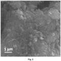
- the material of the active layer as verified in the scanning electron microscopy image ( Figure 2 ), has an average particle size of 185(7) nm and a mode of 133(4) nm, following a log-normal distribution ( Figure 3 ). These particles are rich in graphene with few atomic layers, as can be seen in the transmission electron microscopy image of the scheme in Figure 4 (middle image).
- the electromagnetic spectra of non-oxidized carbon-based compounds have a strong absorption with a maximum around ⁇ 260 nm with a spectral width between 220-350 nm ( Figure 5 ).
- the number of defects generated during high-energy grinding it is observed, in the confocal Raman microscopy spectrum corresponding to the sample of the material that forms the active layer of the sensor after grinding for 100 minutes, where a considerable increase in the bands associated with defects (D and D' in Figure 6 ) can be seen.
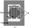
- the sensor device ( Figure 7 ) is made of an FR4 substrate (1) with a thickness of 0.6 mm in this example, on which the interdigitated electrodes (2) of copper coated with gold are located.
- the width of each electrode as the space between them is equal to 0.15 mm and the confined area between the electrodes is 1.2 mm x 1.2 mm in this example.
- the active layer (3) is placed on the substrate and the electrodes, connecting to said electrodes.
- the resistance between the electrodes is monitored and allows, on the one hand, to determine when the solvent of a colloidal drop has evaporated (stabilized resistance value) and, on the other hand, to determine the threshold resistance established at 10 k ⁇ ⁇ 1 k ⁇ for this example. This value ensures electrical contact between the sensitive layer and the electrodes, allowing a reduced noise level.
- the sensor device is located in a watertight chamber, to control the quantities of the gases and their flows exactly.
- This sealed cell allows to circulate a constant synthetic air flow of 100 ml ⁇ min -1 .
- consecutive exposure and purge measurements are performed and the sensitivity, response and recovery times, selectivity against ammonia (subsequent example 2) and the influence of humidity (subsequent example 3) are evaluated.
- the sensor is exposed to -500 ppb of NO 2 for 30 min and then purged for a long period of time. This step is performed with and without photoactivation using a -275 nm LED with a light power of -11.5 mW.
- the sensor used in this example is the same as that used in Example 1. Therefore, the structural and optical characterization, the integration circuit design and the set-up measurement conditions are identical.
- the sensor used in this example is the same as that used in Example 1. Therefore, the structural and optical characterization, the integration circuit design and the set-up measurement conditions are identical.
- the sensor is designed to detect very low concentrations of NO 2 even working in scenarios with ambient relative humidity.
- values of 0%, 10% and 33% are used and a gradual enhanced signal is collected as the relative humidity increases ( Figure 11 ).
- the highest response is obtained for the case of 33% relative humidity with a value of 17%.
- the recovery of the signal tending to the threshold resistance has a higher gradient also as the relative humidity increases. This is due to the fact that, since water molecules react with those of NO 2 , their desorption is easier.
- the senor has a low interaction with the water molecules in the environment due, in this case, to a certain hydrophobic character of the carbon-based compounds, because the nanostructured particles have a reduced number of free radicals, mainly hydroxyls, which are key for interaction with these molecules.
Landscapes
- Chemical & Material Sciences (AREA)
- Health & Medical Sciences (AREA)
- Life Sciences & Earth Sciences (AREA)
- General Health & Medical Sciences (AREA)
- Immunology (AREA)
- Physics & Mathematics (AREA)
- Pathology (AREA)
- General Physics & Mathematics (AREA)
- Analytical Chemistry (AREA)
- Biochemistry (AREA)
- Engineering & Computer Science (AREA)
- Electrochemistry (AREA)
- Chemical Kinetics & Catalysis (AREA)
- Organic Chemistry (AREA)
- Nanotechnology (AREA)
- Materials Engineering (AREA)
- Inorganic Chemistry (AREA)
- Combustion & Propulsion (AREA)
- Food Science & Technology (AREA)
- Medicinal Chemistry (AREA)
- Investigating Or Analyzing Materials By The Use Of Fluid Adsorption Or Reactions (AREA)
Abstract
Description
- The present invention relates to a resistive chemical sensor with a low detection limit for the presence of NO2 at room temperature that comprises a material as active layer of the sensor that is of graphene of few atomic layers, and whose response is not modified by the presence of ambient relative humidity and that, in addition, shows very low interference with ammonia, which makes it possible to rule out its interference in the measurements.
- Nitrogen dioxide (NO2) is a toxic gas and detrimental to health that is primarily formed in power plants due to combustion processes carried out at high temperatures and in all types of combustion engines. This compound is also concentrated in the air of cities as it is derived from carbon monoxide emissions produced by automobiles and domestic heaters when oxidized. In addition, NO2 contributes to the formation of ground-level ozone, of acid rain, and of photochemical smog. From the physiological point of view, breathing high concentrations of NO2 is related to a series of detrimental effects such as spasms, burns, dilation of throat and upper respiratory tract tissues (reduces oxygenation of the body tissues and produces liquid build-up in the lungs [Bylin, G., Lindvall, T., Rehn, T., & Sundin, B. (1985). Effects of short-term exposure to ambient nitrogen dioxide concentrations on human bronchial reactivity and lung function. European Journal of Respiratory Diseases, 66(3), 205-217]. Indirectly, and since it is one of the causes of fine particulate matter PM2.5 (suspended particles of less than 2.5 microns) and it is related to multiple mental diseases (e.g., autism), cardiovascular diseases (e.g., stroke), kidney diseases, and/or cancers. Related to this latter disease, NO2 is the precursor of a particulate matter declared a
Group 1 human carcinogen in October 2013. In accordance with European regulation, the Scientific Committee on Occupational Exposure Limits (SCOEL) of the European Commission establishes at 0.5 ppm and 1 ppm the weighted average values of exposure to NO2 over 8 hours and the short-term exposure limits, respectively. Therefore, a great need arises in the design of highly sensitive gas sensors capable of alerting or warning of the presence of NO2 below these limits, reaching the sub-ppm range. - Research in resistive sensors has been carried out intensively for decades and is currently one of the main technologies used for the detection of domestic, commercial, and industrial gases (
EP1042666 ). The main current challenge is to avoid the high probability of false positives and negatives that the detection of chemical species entails with these devices due to their low selectivity, since a resistive sensor has a response for practically all the gases with which it interacts, also accounting for those that are not of interest (called interfering gases, since they produce a change in the signal of the device that makes its interpretation difficult). Consequently, a great deal of research is focused on the search for sensors with higher selectivity following various strategies such as doping the base material with metallic elements (CN106770498A ), decorating with different materials [Matatagui, D., Sainz- Vidal, A., Grácia, I., Figueras, E., Cañé, C., & Saniger, JM (2018a). Chemoresistive gas sensor based on ZIF-8/ZIF-67 nanocrystals. Sensors and Actuators, B: Chemical, 274] and/or the evaluation of the maximum sensitivity temperatures for each particular gas [Ponzoni, A., Baratto, C., Cattabiani, N., Falasconi, M., Galstyan, V., Nunez-Carmona, E., ... Zappa, D. (2017). Metal Oxide Gas Sensors, a Survey of Selectivity Issues Addressed at the SENSOR Lab, Brescia (Italy). Sensors, 17(4), 714], in no instance is total selectivity achieved for a given gas in a mixture of gases. - Within resistive sensors, semiconductor materials based on metal oxides stand out for their different response depending on whether they are p-type (electrical conduction preferably by holes) or n-type (electrical conduction preferably by electrons), allowing the classification of the gases to be detected in two large groups: oxidants and reducers. For example, if you have a p-type material and it is exposed to an oxidizing gas to which it is sensitive, its electrical resistance decreases as a greater number of holes are generated. On the other hand, if it is a reducing gas, its electrical resistance increases as the number of holes decreases [Matatagui, D., Sainz-Vidal, A., Grácia, I., Figueras, E., Cañé, C., & Saniger, J.M. (2018a). Chemoresistive gas sensor based on ZIF-8/ZIF-67 nanocrystals. Sensors and Actuators, B: Chemical, 274]. If you have an n-type material, opposite responses to those described above occur [Maeng, S., Kim, S.-W., Lee, D.-H., Moon, S. - E., Kim, K.-C., & Maiti, A. (2013). SnO2 Nanoslab as NO2 Sensor: Identification of the NO2 Sensing Mechanism on a SnO2 Surface]. A priori, these selective responses could be an advantage, since a semiconductor device could perfectly distinguish between oxidizing and reducing gases, however, exposure to an environment with mixtures of oxidizing and reducing gases could provide an erroneous sensor response, obtaining, mainly, false negatives because the signals can be counteracted. This result would become the worst-case scenario because a subject could be exposed to a high concentration of two gases that are harmful to health and the sensor would not give any alarm. Another important interference in the sensor's response that could compromise its correct operation is that produced by environmental humidity. This factor is crucial since virtually any real technological application involves measuring with a baseline environmental humidity and, on many occasions, it causes the device to lose sensitivity to the gas of interest [Wozniak, L, Kalinowski, P., Jasinski, G., & Jasinski, P. (2018). FFT analysis of temperature modulated semiconductor gas sensor response for the prediction of ammonia concentration under humidity interference. Microelectronics Reliability, 84, 163-169]
- Widely used metal oxide semiconductors (for example, SnO2 [Zhong, Y., Li, W., Zhao, X., Jiang, X., Lin, S., Zhen, Z., ... Zhu, H (2019). High-Response Room-Temperature NO2 Sensor and Ultrafast Sensor Based on SnO2 with Rich Oxygen Vacancy [Research-article]. ACS Applied Materials and Interfaces, 11 (14), 13441-13449]) as mentioned before, possess a low concentration of charge carriers at room temperature and, therefore, these materials require operating at high temperatures, through external heating, which causes an increased risk of ignition and an increase in energy expenditure. As a possible solution to these problems, the use of carbon-based nanomaterials is currently being investigated since they can operate at room temperature with a high mobility of charge carriers. However, among these nanomaterials, pristine graphene is a relatively chemically inert material, as it does not interact with the chemical elements found in its surrounding environment; graphene oxide has an insulating character, with a low density of charge carriers, an adverse factor for obtaining a sensor device that works based on a change in resistivity/conductivity; and reduced graphene oxide which, although it has part of the functional groups of graphene oxide (epoxide, carboxyl, and/or hydroxyl groups), has semiconductor electrical properties, which has allowed the development of resistive sensors with high efficiency in the detection of NO2 [
CN104181209A ], these functional groups also display a strong interaction with some interferents such as ammonia and humidity, hindering their use in real environments due to the difficulty of adequately interpreting the sensor response. - Therefore, there is currently the problem of an NO2 sensor that combines in a single device reproducibility, absence of false positives and negatives, high chemical stability, reduced dimensions, the possibility of integrating it into different technologies such as silicon, printed circuits and flexible circuits and high selectivity, that is, low interference with other compounds such as ammonia (NH3) and the presence of humidity (H2O in the form of vapor in different percentages), in a working range at room temperature of between 10°C and 30°C.
- In a first aspect, the present invention relates to a resistive chemical sensor for the detection of NO2, characterized in that it comprises
- an insulating substrate;
- at least two metallic electrodes on the insulating substrate;
- at least one active layer located on the substrate and the electrodes, connecting said metallic electrodes, where the active layer has a thickness between 20 nm and 100 µm and is made up of particles with a size between 20 nm and 1000 nm agglomerated and nanostructured in nanodomains, where said nanodomains are of non-oxidized graphene with few atomic layers, where said graphene contains structural defects, and where said defects are carbon vacancies in the structure of the graphene with few atomic layers.
- In the present invention "graphene with few atomic layers" is understood as having an ordered stacking of 3 to 10 layers of graphene [ISO/TS 80004-13:2017(E)]; it is a nanostructured material that has not been subjected to chemical oxidation and reduction treatments, and that has a high number of structural defects generated during its production, where said defects serve as active sites of chemical reaction to achieve high sensitivity and high selectivity at room temperature, and whose performance is not devalued with environmental humidity. Therefore, they present a high density of charge carriers. These structural defects are caused by the high-energy mechanical grinding process used on the precursor material. In the present invention, for obtaining said material of the active active layer in the sensor of the present invention is characterized in that it comprises the following stages:
- (a) grinding graphite flakes by means of a high-energy oscillatory dry mechanical method, for a time of at least 80 min at a grinding speed between 1300 and 1700 rpm, and at a temperature between 15°C and 35°C;
- (b) dispersing the powder obtained in step (a) in an organic solvent selected from 1-methyl-2-pyrrolidinone, dimethylformamide or dimethylsulfoxide, and wherein the concentration range varies between 0.1 mg/mL and 10 mg/mL; and
- (c) drip depositing the solution obtained in step (b) on an integrating circuit comprising an insulating substrate with at least two metallic electrodes on said substrate and evaporating the solvent in the air;
- The measurement of the resistance in step (c) allows, on the one hand, to determine when the solvent of a colloidal drop has evaporated (stabilized resistance value) and, on the other hand, to determine the established threshold resistance, which will depend on the design of the device, that is, the materials used and their sizes and thicknesses, the material of the electrodes, and the active layer. The deposition process is repeated until a stable and low-noise resistance/conductance signal is obtained, ensuring electrical contact between the electrodes through the layer.
- The material that comprises graphene with few atomic layers, shows an electrical behaviour characteristic of a p-type semiconductor wherein the number of holes is increased by the high charge transfer that occurs when interacting with an oxidizing gas, such as NO2. This gas mainly interacts with the defects of the nanostructures, which give the sensor device high sensitivity. The low number of functional groups (free radicals), provide the optimized nanostructures with a very low interaction with NH3 molecules (reducing in nature). Likewise, due to this low number of reacting radicals and the hydrophobicity of carbon-based compounds, the relative humidity of the environment practically does not modify the signal of the designed sensor, ensuring its operation in the typically humid environments. Lastly, despite the excellent response of the sensor to NO2, it is possible to improve the speed of adsorption and desorption of the NO2 molecules by means of a photoactivation process in the ultraviolet range, because the material of the active layer absorbs in the range of that radiation, causing their activation with light in a faster manner for adsorption and fundamentally for desorption, where the process is more stable and stronger.
- Therefore, the material that forms the active layer of the present invention has not been subjected to any chemical attack to obtain oxygenated functional groups to improve interaction with environmental compounds.
- Accordingly, all the advantages of such a sensor are:
- its low detection limit of NO2, with a presence of 25 ppb at room temperature, where the sensor would already begin to detect said gas and whose response is not drastically modified by the presence of ambient relative humidity;
- very low interference with ammonia (reducing agent with a great impact on health and the environment);
- improvement of the response, i.e., it becomes more sensitive to the presence of the gas and the speed of said response, by exposure to UV radiation;
- easy low-cost industrial upscaling.
- In a preferred embodiment of the sensor of the present invention, the insulating substrate is formed of a material selected from FR4, silicon, alumina, polymers, plastics, paper, gallium arsenide, aluminium nitride and glass. In a more preferred embodiment, the insulating substrate is FR4. The advantage associated to FR4 is due to its ease of manufacture and being one of the most used in electronic developments.
- In another preferred embodiment of the sensor of the present invention, the electrodes are at least two and the conductive material that forms them is selected from among copper, gold, platinum, aluminium, chromium, titanium, silver and any alloy thereof or copper coated with a material selected from among gold, platinum chrome, titanium any combination of the foregoing. In a more preferred embodiment, the electrodes are two and the conductive material that forms them is copper coated with gold. The advantage associated with copper coated with gold is due to its good adhesion to the substrate.
- In another preferred embodiment of the sensor, the electrodes are interdigitated, with a space between the electrodes of between 1 µm and 1000 µm, thus improving the electrical contact with the active material, and thereby the noise being lower and the values of resistance more stable.
- In a more preferred embodiment of the sensor of the present invention, the electrodes are 2, they are of copper coated with gold, both electrodes being interdigitated, with a space between the electrodes of between 25 µm and 250 µm, and wherein the confined area between the electrodes is between 0.04 mm2 to 4 mm2.
- In another preferred embodiment of the sensor of the present invention, the size of the particles of the active layer is between 50 nm and 450 nm.
- In another preferred embodiment of the sensor of the present invention the active layer has an absorbance an absorption spectrum in the ultraviolet-visible region with an absorption maximum located between 200 and 400 nm. In a more preferred embodiment of the sensor, the absorption maximum is located between 250 nm and 270 nm.
- In another preferred embodiment of the sensor of the present invention, the active layer presents a Raman spectrum comprising 4 characteristic bands, where said bands are D, G, D' and 2D, wherein the relationship between the amplitudes between the D and G bands has a value comprised between 0.6 and 1.5, and wherein the ratio between the amplitudes of the bands D' and G has a value comprised between 0.1 and 0.4.
- In another preferred embodiment of the sensor, it also comprises a flow controller to circulate air towards the active layer.
- In another preferred embodiment of the sensor of the present invention, said sensor is located in a chamber. In a more preferred embodiment, said chamber is watertight.
- In another embodiment of the sensor of the present invention, it also comprises the appropriate means to close the circuit with the electrodes and the active layer. In another more preferred embodiment of the sensor, it also comprises the appropriate means to measure and/or visualize the resistance thereof.
- A second aspect of the present invention is the process for obtaining the resistive NO2 gas sensor described above characterized in that it comprises the following steps
- (a) grinding graphite flakes by means of a high-energy oscillatory dry mechanical method, for a time of at least 80 min at a grinding speed of between 1300 and 1700 rpm, and at a temperature between 15°C and 35°C;
- (b) dispersing the powder obtained in step (a) in an organic solvent selected from 1-methyl-2-pyrrolidinone, dimethylformamide or dimethylsulfoxide, and wherein the concentration range varies between 0.1 mg/ml and 10 mg/ml; and
- (c) drip depositing the solution obtained in step (b) on an integrating circuit comprising an insulating substrate with at least two metallic electrodes on said substrate and evaporating the solvent in the air;
- In a preferred embodiment of the process, during the mechanical grinding of step (a), pauses in said grinding are made every 15 min and 30 minutes until the thermalization of the material and of the grinding equipment is reached at a temperature between 15°C and 35°C. In this way, homogeneous samples with a large amount of graphene with few atomic layers are obtained, and thus avoiding undesired increases in temperature inside the container generated by friction during oscillatory dry grinding and thus avoiding problems with the effective exfoliation process for obtaining the active layer of graphene with few atomic layers and/or the generation of undesired secondary phases.
- In the present invention, "graphite flakes" are understood as monocrystalline graphite in the form of flakes, and wherein each graphite flake is between 2 µm and 50 µm in length and with a thickness of less than 100 nm.
- In a preferred embodiment, the mechanical grinding of stage (a) is carried out in a ball mill in a metal container whose interior is coated with a material selected from among those with a Knoop hardness greater than 1,000 kg/mm2, preferably tungsten carbide, and adding at least one ball of the same material that covers the interior of the metal container, and that meets a mass ratio between the ball or balls and the graphite used of between 1:20 and 1:30, the volume ratio between the ball or balls and the precursor graphite powder is between 0.8:1 and 1.2:1, preferably 1:1, and the volume ratio between the ball or balls and the container receptacle is between 1:48 and 1:52, preferably 1:50. A material of said hardness or higher is used as the lining of the container and as the material of the mill balls to avoid contamination and/or the formation of undesired phases.
- In a preferred embodiment of the process, the grinding time of step (a) is between 80 min and 500 min. In another more preferred embodiment, the time is between 80 min and 300 min. In another even more preferred embodiment, the time is between 80 min and 200 min. In an even more preferred embodiment, the time is between 80 min and 120 min.
- In another preferred embodiment of the process, the organic solvent is 1-methyl-2-pyrrolidinone.
- In another preferred embodiment of the process, when the resistance between the electrodes is measured during step (c) of drip depositing, the resistance measured between each deposited drop is stable, remaining without a change of more than 10% of the resistance for a time of 1 min, before depositing the next drop of the process of step (c). In this way it is confirmed that all the solvent of each deposited drop is evaporating and, on the other hand, the threshold resistance value of the sensor is established once there are no differences between the resistance measurements after each deposited drop.
- Another aspect of the invention refers to the use of the sensor described above, to detect the presence of NO2 in a concentration of at least 25 ppb in air at a temperature between 15°C and 35°C.
- In another preferred embodiment of the use, the sensor is exposed to ultraviolet radiation between 200 nm and 400 nm, which would decrease the concentration of the detection limit and the response time between 1% and 4%, but fundamentally the time of recovery.
- In another preferred embodiment of the use, if in the air there is any of the elements selected from the following list NH3, relative humidity between 0.5% and 40% and any combination of the above, the presence of NO2 is detected at a concentration of at least 25 ppb in air at a temperature between 15°C and 35°C.
- A final aspect of the present invention is a method of using the sensor of the present invention characterized in that it comprises the following steps
- a) circulating reference air, without NO2, with a flow of 25 mL/min to 1000 mL/min, established by means of a flow controller, through a chamber where the sensor described according to any of
claims 1 to 7 is located, for a time between 10 min and 30 min so that the resistance of the sensor has a stable initial value; - b) exposing the sensor of step (a) to air to detect the presence of NO2 until at least the value of the response of the sensor is three times its noise, for a maximum time of 30 min; and
- c) purging the air inside the chamber for a time between 10 min and 30 min; optionally during step (a) and (b) the sensor is exposed to ultraviolet radiation of between 200 nm and 400 nm, more preferably of between 260 nm and 280 nm.
- In a preferred embodiment of the method, the chamber of step (a) is watertight and the circulating air flow is between 80 ml·min-1 and 120 ml·min-1.
- In another preferred embodiment of the method, the purging of step (c) is carried out by circulating air, synthetic air, nitrogen, argon, and any combination thereof through the chamber.
- In another embodiment of the method, all steps of said method are carried out at a temperature between 15°C and 35°C.
- Throughout the description and claims the word "comprise" and its variants are not intended to exclude other technical characteristics, additives, components or steps. Other objects, advantages and features of the invention will be apparent to those skilled in the art in part from the description and in part from the practice of the invention. The following examples and figures are provided by way of illustration and are not intended to be limiting of the present invention.
-
-
Fig 1 . X-ray diffraction diagram of the material comprising the active layer and comparison with the graphite flake material. -
Fig. 2 . Scanning electron microscopy (SEM) image of the material comprising the active layer. -
Fig. 3 . Particle size distribution of the material comprising the active layer. -
Fig. 4 . Morphology of graphene nanostructures with few atomic layers by high-resolution transmission electron microscopy (HRTEM) that make up the active layer. -
Fig. 5 . Electromagnetic absorption spectrum in the visible-ultraviolet range of the material comprising the active layer and comparison with the graphite flake material. -
Fig. 6 . Confocal Raman spectrum of the material comprising the active layer and comparison with the graphite flake material. -
Fig. 7 . Diagram of the sensor of example 1. This sensor is made up of an insulating substrate (1), at least two electrodes (2) and an active layer (3). -
Fig. 8 . Micropipette (4) that generates droplets from the dispersion of nanostructured particles (5) in graphene domains with few atomic layers. These drops are deposited on the substrate (1) with the interdigitated electrodes (2) to obtain the sensitive layer of the NO2 sensor. -
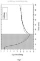
Fig. 9 . Real-time response of the sensor at room temperature for 0.5 ppm of NO2 with and without UV radiation of the sensor of example 1. -
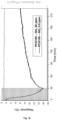
Fig. 10 . Real-time response of the sensor at room temperature for 50 ppm NH3 with UV radiation. The one obtained for 0.5 ppm of NO2 with UV radiation from the sensor of example 1 is added for comparison. -
Fig. 11 . Real-time response of the sensor at room temperature for 0.5 ppm NO2 and relative humidity of 0%, 10% and 33%, at room temperature (25 °C) and with UV radiation of the sensor of example 1. - Next, the invention will be illustrated by some tests carried out by the inventors, which show the effectiveness of the product of the invention.
- Firstly, with respect to the structural and morphological properties, the material that forms the active layer is obtained by 100 minutes of mechanical grinding at 1500 rpm, and the product obtained has an X-ray diffraction pattern characteristic of graphite confined in the nanoscale due to the large width of the diffraction maxima present (
Figure 1 ). In addition, the material of the active layer, as verified in the scanning electron microscopy image (Figure 2 ), has an average particle size of 185(7) nm and a mode of 133(4) nm, following a log-normal distribution (Figure 3 ). These particles are rich in graphene with few atomic layers, as can be seen in the transmission electron microscopy image of the scheme inFigure 4 (middle image). Finally, considering the optical properties, the electromagnetic spectra of non-oxidized carbon-based compounds have a strong absorption with a maximum around ~260 nm with a spectral width between 220-350 nm (Figure 5 ). In relation to the number of defects generated during high-energy grinding, it is observed, in the confocal Raman microscopy spectrum corresponding to the sample of the material that forms the active layer of the sensor after grinding for 100 minutes, where a considerable increase in the bands associated with defects (D and D' inFigure 6 ) can be seen. - The sensor device (
Figure 7 ) is made of an FR4 substrate (1) with a thickness of 0.6 mm in this example, on which the interdigitated electrodes (2) of copper coated with gold are located. The width of each electrode as the space between them is equal to 0.15 mm and the confined area between the electrodes is 1.2 mm x 1.2 mm in this example. On the substrate and the electrodes, connecting to said electrodes, the active layer (3) is placed. - During the deposition process (
Figure 8 ) of the particles, drop by drop using a micropipette (4), which generates drops of the dispersion of nanostructured particles (5), the resistance between the electrodes is monitored and allows, on the one hand, to determine when the solvent of a colloidal drop has evaporated (stabilized resistance value) and, on the other hand, to determine the threshold resistance established at 10 kΩ ± 1 kΩ for this example. This value ensures electrical contact between the sensitive layer and the electrodes, allowing a reduced noise level. - Once the sensitive layer is deposited in the integrating circuit and stabilized with the drying process, the sensor device is located in a watertight chamber, to control the quantities of the gases and their flows exactly. This sealed cell allows to circulate a constant synthetic air flow of 100 ml·min-1. To determine the real performance of this example of NO2 sensor, consecutive exposure and purge measurements are performed and the sensitivity, response and recovery times, selectivity against ammonia (subsequent example 2) and the influence of humidity (subsequent example 3) are evaluated. In a first measurement, the sensor is exposed to -500 ppb of NO2 for 30 min and then purged for a long period of time. This step is performed with and without photoactivation using a -275 nm LED with a light power of -11.5 mW.
- The sensor response is calculated by the equation:

- In
Figure 9 it can be seen how the sensor has a high response (according to the previous formula) to NO2, approximately 14% without ultraviolet radiation. However, this response is improved with the photo-activation process with ultraviolet radiation, reaching a response of approximately 16%. In addition, the photoactivation process allowed to obtain a faster recovery of the initial resistance of the sensor during the purging process compared to the case of absence of ultraviolet radiation. - It was calculated based on 100 measurements that the noise level of the sensor is below -0.25% (calculated as the largest difference of the resistance values of 100 measurements of the sensor resistance in air). Therefore, if it is assumed that the limit of detection is obtained for a signal that must exceed 3 times the noise level of the sensor (0.25% x 3 = 0.75%), concentrations of up to ~25 ppb of NO2 can be detected. Specifically, the maximum gradient of the evolution of the response in real time of the sensor with photoactivation is also calculated and a value of 1.4% per minute is obtained. This result means that NO2 can be detected relatively quickly in environments with a concentration of -500 ppb.
- The sensor used in this example is the same as that used in Example 1. Therefore, the structural and optical characterization, the integration circuit design and the set-up measurement conditions are identical.
- Specifically for this experiment, where the selectivity of the designed sensor is evaluated, one of the main advantages is its very low response to NH3.
Figure 10 shows that the sensor response increases by -1% by introducing 50 ppm. This low sensor response, compared to the -16% obtained for 0.5 ppm NO2, gives the sensor high selectivity. Otherwise, the presence of NH3 could attenuate or cancel the response to NO2, giving rise to false negatives and, therefore, it would be an interferent that restricts the applicability of the sensor device. This low interaction with NH3 fits into an interaction model in which the nanostructured particles contain few free radicals attached onto their surface with which they can interact (such as epoxide, amino, carboxyl and/or hydroxyl groups). - The sensor used in this example is the same as that used in Example 1. Therefore, the structural and optical characterization, the integration circuit design and the set-up measurement conditions are identical.
- The sensor is designed to detect very low concentrations of NO2 even working in scenarios with ambient relative humidity. In this experiment, values of 0%, 10% and 33% are used and a gradual enhanced signal is collected as the relative humidity increases (
Figure 11 ). Specifically, the highest response is obtained for the case of 33% relative humidity with a value of 17%. In addition, the recovery of the signal tending to the threshold resistance has a higher gradient also as the relative humidity increases. This is due to the fact that, since water molecules react with those of NO2, their desorption is easier. On the other hand, as in the case of NH3, it is shown that the sensor has a low interaction with the water molecules in the environment due, in this case, to a certain hydrophobic character of the carbon-based compounds, because the nanostructured particles have a reduced number of free radicals, mainly hydroxyls, which are key for interaction with these molecules. These results make the sensor designed in the present invention a potential tool to effectively prevent health and environmental problems by operating at room temperature and in both reducing (NH3) and humid environments.
Claims (15)
- A resistive chemical sensor for the detection of NO2 characterized in that it comprises• an insulating substrate;• at least two metallic electrodes on the insulating substrate;• at least one active layer located on the substrate and the electrodes, connecting said metallic electrodes, wherein the active layer has a thickness between 20 nm and 100 µm and is made up of particles of a size between 20 nm and 1000 nm agglomerated and nanostructured in nanodomains, where said nanodomains are of non-oxidized graphene with few atomic layers, wherein said graphene contains structural defects, and wherein said defects are carbon vacancies in the structure of graphene with few atomic layers.
- Chemical sensor according to claim 1, wherein the insulating substrate is made of a material selected from FR4, silicon, alumina, polymers, plastics, paper, gallium arsenide, aluminium nitride and glass.
- Chemical sensor according to any one of claims 1 or 2, wherein the electrodes are at least two and the conductive material that forms them is selected from among copper, gold, platinum, aluminium, chromium, titanium, silver and any alloy thereof, or copper coated with a material selected from gold, platinum, chrome, titanium and any combination thereof.
- Chemical sensor according to claim 3, wherein the electrodes are of copper coated with gold and both electrodes are interdigitated, with a space between the electrodes between 25 µm and 250 µm, and wherein the confined area between the electrodes is between 0.04 mm2 of 4 mm2.
- Chemical sensor according to any one of claims 1 to 4, wherein the size of the particles of the active layer is between 50 nm and 450 nm.
- Chemical sensor according to any one of claims 1 to 5, wherein the active layer has an absorbance in the ultraviolet-visible region with an absorption maximum located between 200 and 400 nm.
- Chemical sensor according to any one of claims 1 to 6, wherein the active layer has a Raman spectrum comprising 4 characteristic bands, wherein said bands are D, G, D' and 2D, wherein the ratio between the amplitudes of the bands D and G has a value between 0.6 and 1.5, and wherein the ratio between the amplitudes of the bands D' and G has a value between 0.1 and 0.4.
- Process for obtaining the resistive chemical sensor according to any one of claims 1 to 7, characterized in that it comprises the following steps(a) grinding graphite flakes by means of a high-energy oscillatory dry mechanical method, for a time of at least 80 min at a grinding speed between 1300 and 1700 rpm, and at a temperature between 15 °C and 35 °C;(b) dispersing the powder obtained in step (a) in an organic solvent selected from 1-methyl-2-pyrrolidinone, dimethylformamide or dimethylsulfoxide, and wherein the concentration range varies between 0.1 mg/mL and 10 mg/mL; and(c) drip depositing the solution obtained in step (b) on an integrating circuit comprising an insulating substrate with at least two metallic electrodes on said substrate and evaporating the solvent in the air;optionally, during the step (c) of drip depositing, the resistance between the electrodes is measured.
- Process for obtaining the chemical sensor according to claim 8, wherein the grinding time of step (a) is between 80 min and 120 min.
- Process for obtaining the chemical sensor according to any one of claims 8 or 9, wherein the organic solvent is 1-methyl-2-pyrrolidinone.
- Process for obtaining the chemical sensor according to any of claims 8 to 10, wherein the resistance between the electrodes is measured during step (c) of drip depositing, until the resistance measured between each drop deposited is stable, the resistance remaining without a change greater than 10% for a time of 1 min before depositing the next drop.
- Use of the sensor according to any one of claims 1 to 7 for detecting the presence of NO2 in a concentration of at least 25 ppb in air at a temperature between 15°C and 35°C.
- Use according to claim 12, wherein the sensor is exposed to ultraviolet radiation between 200 nm and 400 nm, preferably between 250 nm and 270 nm.
- Use according to any one of claims 12 or 13, wherein if in the air there is any of the elements selected from the following list NH3, relative humidity between 0.5% and 40% and any combination thereof, the presence of NO2 is detected at a concentration of at least 25 ppb in air at a temperature between 15 °C and 35 °C.
- Method for detecting the presence of NO2 in air, characterized in that it comprises the following steps:a) circulating reference air, without NO2, with a flow of 25 mL/min to 1000 mL/min, established by means of a flow controller, through a chamber where the sensor described according to any of claims 1 to 7 is placed for a time between 10 min and 30 min so that the resistance of the sensor has a stable initial value;b) exposing the sensor of step (a) to air to detect the presence of NO2 until at least the value of the response of the sensor is three times its noise, for a maximum time of 30 min; andc) purging the air inside the chamber for a time between 10 min and 30 min; optionally during step (a) and (b) the sensor is exposed to ultraviolet radiation between 200 nm and 400 nm, preferably between 250 nm and 270 nm.
Applications Claiming Priority (2)
| Application Number | Priority Date | Filing Date | Title |
|---|---|---|---|
| ES202030712A ES2890726B8 (en) | 2020-07-10 | 2020-07-10 | RESISTIVE CHEMICAL SENSOR FOR THE DETECTION OF NO2 |
| PCT/ES2021/070499 WO2022008782A1 (en) | 2020-07-10 | 2021-07-09 | Chemiresistive sensor for detecting no2 |
Publications (4)
| Publication Number | Publication Date |
|---|---|
| EP4180802A1 true EP4180802A1 (en) | 2023-05-17 |
| EP4180802A4 EP4180802A4 (en) | 2024-07-24 |
| EP4180802B1 EP4180802B1 (en) | 2025-10-29 |
| EP4180802C0 EP4180802C0 (en) | 2025-10-29 |
Family
ID=79552833
Family Applications (1)
| Application Number | Title | Priority Date | Filing Date |
|---|---|---|---|
| EP21837464.3A Active EP4180802B1 (en) | 2020-07-10 | 2021-07-09 | Chemiresistive sensor for detecting no2 |
Country Status (4)
| Country | Link |
|---|---|
| US (1) | US12442784B2 (en) |
| EP (1) | EP4180802B1 (en) |
| ES (1) | ES2890726B8 (en) |
| WO (1) | WO2022008782A1 (en) |
Family Cites Families (7)
| Publication number | Priority date | Publication date | Assignee | Title |
|---|---|---|---|---|
| WO1999034199A1 (en) | 1997-12-31 | 1999-07-08 | Corning Incorporated | Metal oxide sensor for detecting nitrogen oxides |
| CN104181209A (en) | 2014-08-14 | 2014-12-03 | 电子科技大学 | Nitrogen dioxide gas sensor and preparation method thereof |
| TWI601956B (en) * | 2015-11-20 | 2017-10-11 | 長庚大學 | Gas sensing unit and producing method thereof |
| US9869651B2 (en) * | 2016-04-29 | 2018-01-16 | Board Of Regents, The University Of Texas System | Enhanced sensitivity of graphene gas sensors using molecular doping |
| WO2017213929A1 (en) * | 2016-06-07 | 2017-12-14 | Board Of Regents, The University Of Texas System | Integration of monolayer graphene with a semiconductor device |
| CN106770498B (en) | 2017-01-12 | 2019-03-05 | 吉林大学 | Acetone sensor based on rhodium-doped tin dioxide nanofiber sensitive material prepared by electrospinning technology, preparation method and application |
| CN108828026A (en) * | 2018-06-25 | 2018-11-16 | 哈尔滨工业大学 | A kind of preparation method of the highly sensitive detection nitrogen dioxide gas sensor of room temperature |
-
2020
- 2020-07-10 ES ES202030712A patent/ES2890726B8/en active Active
-
2021
- 2021-07-09 EP EP21837464.3A patent/EP4180802B1/en active Active
- 2021-07-09 WO PCT/ES2021/070499 patent/WO2022008782A1/en not_active Ceased
- 2021-07-09 US US18/015,474 patent/US12442784B2/en active Active
Also Published As
| Publication number | Publication date |
|---|---|
| WO2022008782A1 (en) | 2022-01-13 |
| ES2890726B8 (en) | 2023-05-03 |
| US12442784B2 (en) | 2025-10-14 |
| US20240035996A1 (en) | 2024-02-01 |
| EP4180802A4 (en) | 2024-07-24 |
| ES2890726B2 (en) | 2022-05-23 |
| EP4180802B1 (en) | 2025-10-29 |
| ES2890726A1 (en) | 2022-01-21 |
| EP4180802C0 (en) | 2025-10-29 |
Similar Documents
| Publication | Publication Date | Title |
|---|---|---|
| Yang et al. | Metal-oxide gas sensors for exhaled-breath analysis: A review | |
| Matatagui et al. | Ultrasensitive NO2 gas sensor with insignificant NH3-interference based on a few-layered mesoporous graphene | |
| Absalan et al. | High-performance carbon monoxide gas sensor based on palladium/tin oxide/porous graphitic carbon nitride nanocomposite | |
| Rahman et al. | Fabrication of an acetone sensor based on facile ternary MnO 2/Gd 2 O 3/SnO 2 nanosheets for environmental safety | |
| Pilliadugula et al. | Effect of pH dependent morphology on room temperature NH3 sensing performances of β-Ga2O3 | |
| Qin et al. | Preparation of p-LaFeO₃/n-Fe₂O₃ heterojunction composites by one-step hydrothermal method and gas sensing properties for acetone | |
| Kacem et al. | Gas sensing properties of graphene oxide loaded with SrTiO3 nanoparticles | |
| Kılıç et al. | The effect of Ag loading on gas sensor properties of TiO2 nanorods | |
| Vallejos et al. | Detection of volatile organic compounds using flexible gas sensing devices based on tungsten oxide nanostructures functionalized with Au and Pt nanoparticles | |
| US11029271B2 (en) | Ammonia gas detecting sensor using graphene doped with copper oxide nanopaticles and ammonia gas detecting device comprising the same | |
| JP6518513B2 (en) | Hydrogen detection coloring sensor | |
| Sha et al. | Development of cataluminescence sensor system for benzene and toluene determination | |
| CN107831194A (en) | A kind of nano line cluster WO sensitive to ammonia3‑W18O49Hetero-junction thin-film | |
| Li et al. | One-step green synthesis of Cu 2 O/CuO@ rGO composites for ppt level detection of NO 2 at room temperature | |
| Sari et al. | AACVD grown WO 3 nanoneedles decorated with Ag/Ag 2 O nanoparticles for oxygen measurement in a humid environment | |
| Alev et al. | Effect of Pt catalyst on the sensor performance of WO 3 nanoflakes towards hazardous gases | |
| Zhang et al. | Monolayer self-assembled film of Pd decorated In-doped SnO2 hollow nanospheres for ultrasensitive H2S MEMS gas sensors | |
| Ydir et al. | Aluminum doped zinc oxide nanoplatelets based sensor with enhanced hydrogen sulfide detection | |
| Park et al. | Ultra-sensitive ethanol detection using a chemiresistive SnO2 thin-film gas sensor functionalized with RuO2 nanosheets | |
| EP4180802B1 (en) | Chemiresistive sensor for detecting no2 | |
| Beniwal | SnO 2-ZnO-Fe 2 O 3 tri-composite based room temperature operated dual behavior ammonia and ethanol sensor for ppb level detection | |
| Özdilek et al. | Micro-hotplate gas sensor based on tungsten trioxide (WO3) nanoflakes for detecting chemical warfare agent simulants | |
| Horrillo et al. | Chemiresistive sensor for detecting NO2 | |
| KR102578598B1 (en) | Room temperature operating hydrogen gas sensor based on metal oxide nanostructure functionalized with metal nanoparticle by microwave absorption and manufacturing method thereof | |
| Shao et al. | Room-temperature ethanol sensors based on amorphous Ta2O5/Pd hybrid microspheres |
Legal Events
| Date | Code | Title | Description |
|---|---|---|---|
| STAA | Information on the status of an ep patent application or granted ep patent |
Free format text: STATUS: THE INTERNATIONAL PUBLICATION HAS BEEN MADE |
|
| PUAI | Public reference made under article 153(3) epc to a published international application that has entered the european phase |
Free format text: ORIGINAL CODE: 0009012 |
|
| STAA | Information on the status of an ep patent application or granted ep patent |
Free format text: STATUS: REQUEST FOR EXAMINATION WAS MADE |
|
| 17P | Request for examination filed |
Effective date: 20230210 |
|
| AK | Designated contracting states |
Kind code of ref document: A1 Designated state(s): AL AT BE BG CH CY CZ DE DK EE ES FI FR GB GR HR HU IE IS IT LI LT LU LV MC MK MT NL NO PL PT RO RS SE SI SK SM TR |
|
| DAV | Request for validation of the european patent (deleted) | ||
| DAX | Request for extension of the european patent (deleted) | ||
| RIN1 | Information on inventor provided before grant (corrected) |
Inventor name: PENA MORENO, ALVARO Inventor name: LOPEZ SANCHEZ, JESUS Inventor name: NAVARRO PALMA, ELENA Inventor name: MARIN PALACIOS, PILAR Inventor name: MATATAGUI CRUZ, DANIEL Inventor name: HORRILLO GUEEMES, CARMEN |
|
| REG | Reference to a national code |
Ref country code: DE Ref legal event code: R079 Free format text: PREVIOUS MAIN CLASS: G01N0027040000 Ipc: G01N0027120000 Ref country code: DE Ref legal event code: R079 Ref document number: 602021041466 Country of ref document: DE Free format text: PREVIOUS MAIN CLASS: G01N0027040000 Ipc: G01N0027120000 |
|
| A4 | Supplementary search report drawn up and despatched |
Effective date: 20240625 |
|
| RIC1 | Information provided on ipc code assigned before grant |
Ipc: C01B 32/194 20170101ALI20240619BHEP Ipc: G01N 27/12 20060101AFI20240619BHEP |
|
| GRAP | Despatch of communication of intention to grant a patent |
Free format text: ORIGINAL CODE: EPIDOSNIGR1 |
|
| STAA | Information on the status of an ep patent application or granted ep patent |
Free format text: STATUS: GRANT OF PATENT IS INTENDED |
|
| RIC1 | Information provided on ipc code assigned before grant |
Ipc: C01B 32/194 20170101ALI20250429BHEP Ipc: G01N 27/12 20060101AFI20250429BHEP |
|
| INTG | Intention to grant announced |
Effective date: 20250520 |
|
| GRAS | Grant fee paid |
Free format text: ORIGINAL CODE: EPIDOSNIGR3 |
|
| GRAA | (expected) grant |
Free format text: ORIGINAL CODE: 0009210 |
|
| STAA | Information on the status of an ep patent application or granted ep patent |
Free format text: STATUS: THE PATENT HAS BEEN GRANTED |
|
| AK | Designated contracting states |
Kind code of ref document: B1 Designated state(s): AL AT BE BG CH CY CZ DE DK EE ES FI FR GB GR HR HU IE IS IT LI LT LU LV MC MK MT NL NO PL PT RO RS SE SI SK SM TR |
|
| REG | Reference to a national code |
Ref country code: CH Ref legal event code: F10 Free format text: ST27 STATUS EVENT CODE: U-0-0-F10-F00 (AS PROVIDED BY THE NATIONAL OFFICE) Effective date: 20251029 Ref country code: GB Ref legal event code: FG4D |
|
| REG | Reference to a national code |
Ref country code: IE Ref legal event code: FG4D |
|
| REG | Reference to a national code |
Ref country code: DE Ref legal event code: R096 Ref document number: 602021041466 Country of ref document: DE |
|
| U01 | Request for unitary effect filed |
Effective date: 20251201 |
|
| U07 | Unitary effect registered |
Designated state(s): AT BE BG DE DK EE FI FR IT LT LU LV MT NL PT RO SE SI Effective date: 20251208 |
|
| PG25 | Lapsed in a contracting state [announced via postgrant information from national office to epo] |
Ref country code: NO Free format text: LAPSE BECAUSE OF FAILURE TO SUBMIT A TRANSLATION OF THE DESCRIPTION OR TO PAY THE FEE WITHIN THE PRESCRIBED TIME-LIMIT Effective date: 20260129 |
|
| PG25 | Lapsed in a contracting state [announced via postgrant information from national office to epo] |
Ref country code: HR Free format text: LAPSE BECAUSE OF FAILURE TO SUBMIT A TRANSLATION OF THE DESCRIPTION OR TO PAY THE FEE WITHIN THE PRESCRIBED TIME-LIMIT Effective date: 20251029 |
|
| PG25 | Lapsed in a contracting state [announced via postgrant information from national office to epo] |
Ref country code: RS Free format text: LAPSE BECAUSE OF FAILURE TO SUBMIT A TRANSLATION OF THE DESCRIPTION OR TO PAY THE FEE WITHIN THE PRESCRIBED TIME-LIMIT Effective date: 20260129 |
|
| PG25 | Lapsed in a contracting state [announced via postgrant information from national office to epo] |
Ref country code: IS Free format text: LAPSE BECAUSE OF FAILURE TO SUBMIT A TRANSLATION OF THE DESCRIPTION OR TO PAY THE FEE WITHIN THE PRESCRIBED TIME-LIMIT Effective date: 20260228 |
|
| PG25 | Lapsed in a contracting state [announced via postgrant information from national office to epo] |
Ref country code: PL Free format text: LAPSE BECAUSE OF FAILURE TO SUBMIT A TRANSLATION OF THE DESCRIPTION OR TO PAY THE FEE WITHIN THE PRESCRIBED TIME-LIMIT Effective date: 20251029 |