EP4178067A1 - Charging and discharging device for secondary battery - Google Patents
Charging and discharging device for secondary battery Download PDFInfo
- Publication number
- EP4178067A1 EP4178067A1 EP21869722.5A EP21869722A EP4178067A1 EP 4178067 A1 EP4178067 A1 EP 4178067A1 EP 21869722 A EP21869722 A EP 21869722A EP 4178067 A1 EP4178067 A1 EP 4178067A1
- Authority
- EP
- European Patent Office
- Prior art keywords
- pin
- mounting portion
- current
- secondary battery
- charging
- Prior art date
- Legal status (The legal status is an assumption and is not a legal conclusion. Google has not performed a legal analysis and makes no representation as to the accuracy of the status listed.)
- Granted
Links
Images


Classifications
-
- H—ELECTRICITY
- H02—GENERATION; CONVERSION OR DISTRIBUTION OF ELECTRIC POWER
- H02J—ELECTRIC POWER NETWORKS; CIRCUIT ARRANGEMENTS OR SYSTEMS FOR SUPPLYING OR DISTRIBUTING ELECTRIC POWER; SYSTEMS FOR STORING ELECTRIC ENERGY
- H02J7/00—Circuit arrangements for charging or discharging batteries or for supplying loads from batteries
- H02J7/70—Circuit arrangements for charging or discharging batteries or for supplying loads from batteries characterised by the mechanical construction
- H02J7/751—Circuit arrangements for charging or discharging batteries or for supplying loads from batteries characterised by the mechanical construction concerning the insertion or the connection of the batteries
-
- G—PHYSICS
- G01—MEASURING; TESTING
- G01R—MEASURING ELECTRIC VARIABLES; MEASURING MAGNETIC VARIABLES
- G01R31/00—Arrangements for testing electric properties; Arrangements for locating electric faults; Arrangements for electrical testing characterised by what is being tested not provided for elsewhere
- G01R31/36—Arrangements for testing, measuring or monitoring the electrical condition of accumulators or electric batteries, e.g. capacity or state of charge [SoC]
- G01R31/364—Battery terminal connectors with integrated measuring arrangements
-
- H—ELECTRICITY
- H01—ELECTRIC ELEMENTS
- H01R—ELECTRICALLY-CONDUCTIVE CONNECTIONS; STRUCTURAL ASSOCIATIONS OF A PLURALITY OF MUTUALLY-INSULATED ELECTRICAL CONNECTING ELEMENTS; COUPLING DEVICES; CURRENT COLLECTORS
- H01R13/00—Details of coupling devices of the kinds covered by groups H01R12/70 or H01R24/00 - H01R33/00
- H01R13/02—Contact members
- H01R13/04—Pins or blades for co-operation with sockets
-
- G—PHYSICS
- G01—MEASURING; TESTING
- G01R—MEASURING ELECTRIC VARIABLES; MEASURING MAGNETIC VARIABLES
- G01R27/00—Arrangements for measuring resistance, reactance, impedance, or electric characteristics derived therefrom
- G01R27/02—Measuring real or complex resistance, reactance, impedance, or other two-pole characteristics derived therefrom, e.g. time constant
- G01R27/08—Measuring resistance by measuring both voltage and current
-
- G—PHYSICS
- G01—MEASURING; TESTING
- G01R—MEASURING ELECTRIC VARIABLES; MEASURING MAGNETIC VARIABLES
- G01R31/00—Arrangements for testing electric properties; Arrangements for locating electric faults; Arrangements for electrical testing characterised by what is being tested not provided for elsewhere
- G01R31/36—Arrangements for testing, measuring or monitoring the electrical condition of accumulators or electric batteries, e.g. capacity or state of charge [SoC]
- G01R31/382—Arrangements for monitoring battery or accumulator variables, e.g. SoC
- G01R31/3842—Arrangements for monitoring battery or accumulator variables, e.g. SoC combining voltage and current measurements
-
- G—PHYSICS
- G01—MEASURING; TESTING
- G01R—MEASURING ELECTRIC VARIABLES; MEASURING MAGNETIC VARIABLES
- G01R31/00—Arrangements for testing electric properties; Arrangements for locating electric faults; Arrangements for electrical testing characterised by what is being tested not provided for elsewhere
- G01R31/36—Arrangements for testing, measuring or monitoring the electrical condition of accumulators or electric batteries, e.g. capacity or state of charge [SoC]
- G01R31/385—Arrangements for measuring battery or accumulator variables
- G01R31/3865—Arrangements for measuring battery or accumulator variables related to manufacture, e.g. testing after manufacture
-
- Y—GENERAL TAGGING OF NEW TECHNOLOGICAL DEVELOPMENTS; GENERAL TAGGING OF CROSS-SECTIONAL TECHNOLOGIES SPANNING OVER SEVERAL SECTIONS OF THE IPC; TECHNICAL SUBJECTS COVERED BY FORMER USPC CROSS-REFERENCE ART COLLECTIONS [XRACs] AND DIGESTS
- Y02—TECHNOLOGIES OR APPLICATIONS FOR MITIGATION OR ADAPTATION AGAINST CLIMATE CHANGE
- Y02E—REDUCTION OF GREENHOUSE GAS [GHG] EMISSIONS, RELATED TO ENERGY GENERATION, TRANSMISSION OR DISTRIBUTION
- Y02E60/00—Enabling technologies; Technologies with a potential or indirect contribution to GHG emissions mitigation
- Y02E60/10—Energy storage using batteries
Definitions
- the present disclosure relates to a charging and discharging device for secondary battery, and more particularly to a charging and discharging device for secondary battery having improved contact resistance.
- a secondary battery has attracted considerable attention as an energy source for power-driven devices, such as an electric bicycle, an electric vehicle, and a hybrid electric vehicle, as well as an energy source for mobile devices, such as a mobile phone, a digital camera, a laptop computer and a wearable device.
- such a secondary battery is classified into a cylindrical battery where an electrode assembly is built in a cylindrical metal can, a prismatic battery where an electrode assembly is built in a prismatic metal can, and a pouch type battery where an electrode assembly is built in a pouch type case formed of an aluminum laminate sheet.
- the cylindrical battery has an advantage of having a relatively large capacity and being structurally stable.
- the battery performance of such a secondary battery is evaluated through a charge and discharge process after the assembling process, and whether the battery is defective can be detected.
- the charge and discharge process of the secondary battery can be performed through a secondary battery charging and discharging device including a probe pin to which current and voltage are applied.
- a charging and discharging device for secondary battery comprising: a body portion; and a head portion located under the body portion, wherein the head portion comprises a pin mounting portion that is bound to the upper portion or lower portion of the secondary battery, wherein the pin mounting portion includes a current pin and a voltage pin, wherein the current pin and the voltage pin each comprises a plurality of projections, and wherein an area where the current pin is formed is larger than an area where the voltage pin is formed.
- the current pin may be formed in the maximum area that can be formed in the pin mounting portion, and the voltage pin may be formed in a minimum area that can be formed in the pin mounting portion.
- the current pin may be formed in an area of 70% or more and 99% or less relative to the total area of the pin mounting portion, and the voltage pin may be formed in an area of 1% or more and 15% or less relative to the total area of the pin mounting portion.
- the voltage pin may be formed in the center of the pin mounting portion, and the current pin may be formed at the periphery of the pin mounting portion so as to surround the voltage pin.
- the voltage pin may have a diameter of 0.01 or more and 0.2 or less relative to the diameter of the pin mounting portion.
- the current pin and the voltage pin may be located apart from each other.
- the distance between the current pin and the voltage pin that are spaced apart from each other may be 0.01 or more to 0.5 or less relative to the diameter of the pin mounting portion.
- the current pin may be formed in the center of the pin mounting portion, and the voltage pin may be formed at a periphery of the pin mounting portion so as to surround the current pin.
- the current pin may have a diameter of 0.5 or more and 0.9 or less relative to the diameter of the pin mounting portion.
- the current pin and the voltage pin may be located apart from each other.
- the distance between the current pin and the voltage pin that are spaced apart from each other may be 0.01 or more to 0.5 or less relative to the diameter of the pin mounting portion.
- the charging and discharging device for a secondary battery of the present disclosure can improve the contact resistance.
- planar when referred to as “planar”, it means when a target portion is viewed from the upper side, and when referred to as “cross-sectional”, it means when a target portion is viewed from the side of a cross section cut vertically.
- the secondary battery 10 herein is not limited to a cylindrical battery, and the secondary batteries having various shapes can also be described with same or similar contents.
- Fig. 1 is a partial cross-sectional view of an upper portion of a cylindrical secondary battery.
- the secondary battery 10 can be manufactured by housing an electrode assembly 50 in a cylindrical case 20, and mounting a cap assembly 30 on an opened upper portion of the cylindrical case 20.
- the cap assembly 30 includes an upper end cap 31 and a safety vent 32 for internal pressure drop, and the upper end cap 31 and the safety vent 32 for internal pressure drop may form a structure in close contact with each other.
- the safety vent 32 may be electrically connected to the electrode assembly 50 via a current interrupt device (CID), and a CID gasket 70 can wrap the edge of the current interrupt device 60.
- CID current interrupt device
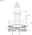
- Fig. 2 is a view showing a charging and discharging device for a secondary battery according to an embodiment of the present disclosure.
- the charging and discharging device 100 for a secondary battery can come into contact with the upper end cap 31 of the secondary battery 10 and apply a charging current.
- the charging and discharging device 100 for a secondary battery includes body portions 110 and 120, a head portion 130, and a pin mounting portion 135.
- the body portions 110 and 120 may be configured by a plurality of plungers.
- the body portions 110 and 120 may include an external plunger 110 having a cylindrical shape through which the inside is penetrated, and an internal plunger 120 that flows up and down in the interior of the external plunger 110.
- the head portion 130 may be located under the internal plunger 120.
- the pin mounting portion 135 may be located under the head portion 130. Further, the pin mounting portion 135 can be bound to the upper portion or lower portion of the secondary battery 100. In one example, the pin mounting portion 100 may be bound to the upper end cap 31 of the secondary battery 10.
- the pin mounting portion 135 includes a current pin 136 and a voltage pin 137.
- each of the current pin 136 and the voltage pin 137 includes a plurality of protrusions.
- the current pin 136 and/or the voltage pin 137 may include a plurality of protrusions having a shape such as conic or triangular pyramid with a pointed tip.
- the current pin 136 and/or the voltage pin 137 can increase the contact area with the cap assembly 30 of the secondary battery 10 and thus, improve the contact resistance by the current pin 136 and/or the voltage pin 137.
- Fig. 3 is an enlarged view of the region A of Fig. 2 .
- Fig. 3(a) is a view showing a state in which the secondary battery 10 is normally bound to the charging and discharging device 100 for a secondary battery
- Fig. 3(b) is a diagram showing a state in which the secondary battery 10 is abnormally bound to the charging and discharging device 100 for a secondary battery.
- the upper end cap 31 and the pin mounting portion 135 can be abnormally bound to each other, in addition to the case where the upper end cap 31 and the pin mounting portion 135 are normally bound.
- a non-contact region B that does not come into contact with the pin mounting portion 135 can be generated at the periphery of the upper end cap 31, unlike Fig 3(a) .
- the charging and discharging device 100 for a secondary battery adjusts the arrangement and area of the current pin 136 and the voltage pin 137, and thus can reduce the non-contact region B of the upper end cap 31 and the contact resistance of the current pin 136.
- the contact resistance by the current pin 136 may be changed in proportion to the area in which the current pin 136 is formed.
- the pin mounting portion 135 is configured such that an area in which the current pin 136 is formed may be larger than an area in which the voltage pin 137 is formed.
- the current pin 136 in the pin mounting portion 135 is formed in the maximum area that can be formed in the pin mounting portion 135, and the voltage pin 137 may be formed in the minimum area that can be formed in the pin mounting portion 135.
- the pin mounting portion 135 of the charging and discharging device 100 for a secondary battery allows the increase of the contact area between the upper end cap 31 and the current pin 136, so that the contact resistance by the current pin 136 can be increased.
- Fig. 4 is a view showing a pin mounting portion 135 according to an embodiment of the present disclosure in the charging and discharging device 100 for a secondary battery of Fig. 2 .
- the pin mounting portion 135 is configured such that a voltage pin 137 is formed in the center of the pin mounting portion 135. Further, in the pin mounting portion 135, the current pin 136 is formed on the periphery of the pin mounting portion 135, and the current pin 136 may be formed so as to surround the voltage pin 137.
- the diameter R3 of the voltage pin 137 may be 0.01 or more and less than 0.25 relative to the diameter R1 of the pin mounting portion 135. More preferably, the diameter R3 of the voltage pin 137 may be 0.01 or more and 0.23 or less relative to the diameter R1 of the pin mounting portion 135. In one example, the diameter R3 of the voltage pin 137 may be 0.01 or more and 0.2 or less relative to the diameter R1 of the pin mounting portion 135.
- the pin mounting portion 135 includes the voltage pin 137 having a diameter that satisfies the above-mentioned range, the area that the voltage pin 137 can be formed in the pin mounting portion 135 can be reduced, so that the area that the current pin 136 can form in the pin mounting portion 135 can be increased. Consequently, referring to Figs. 2 and 4 , in the charging and discharging device 100 for a secondary battery according to an embodiment of the present disclosure, the contact area between the current pin 136 and the upper end cap 31 is increased, so that the contact resistance can be reduced. Further, the occurrence of heat generation phenomenon can be prevented, and the accuracy of the battery performance evaluation of the secondary battery can be improved.
- the pin mounting portion 135 includes a voltage pin 137 in which the diameter R3 of the voltage pin 137 is less than 0.01 relative to the diameter R1 of the pin mounting portion 135, the accuracy of the existence of charging/discharging of the secondary battery measured from the voltage pin may decrease. Further, when the pin mounting portion 135 includes a voltage pin 137 in which the diameter R3 of the voltage pin 137 is greater than 0.25 relative to the diameter R1 of the pin mounting portion 135, the area of the current pin 136 is reduced, whereby a contact resistance may be increased as a current is applied from the current pin 136 to the secondary battery 10.
- the diameter R1 of the pin mounting portion 135 may be the same as or larger than the outer diameter of the current pin 136.
- the pin mounting portion 135 can be configured such that the current pin 136 and the voltage pin 137 are located apart from each other.
- the distance between the current pin 136 and the voltage pin 137 that are spaced apart from each other may be 0.01 or more to 0.5 or less relative to the diameter R1 of the pin mounting portion 135. More preferably, the distance between the current pin 136 and the voltage pin 137 that are spaced apart from each other may be 0.03 or more and 0.4 or less relative to the diameter R1 of the pin mounting portion 135. In one example, the distance between the current pin 136 and the voltage pin 137 that are spaced apart from each other may be 0.05 or more to 0.35 or less relative to the diameter R1 of the pin mounting portion 135.
- the pin mounting portion 135 includes a current pin 136 and a voltage pin 137 having a distance that satisfies the above-described range, the area that the current pin 136 can form is increased and the area that the voltage pin 137 can form in the pin mounting portion 135 can be reduced, so that the contact resistance by the current pin 136 can be reduced.
- the occurrence of a heat generation phenomenon can be prevented, and the accuracy of the battery performance evaluation of the secondary battery can be improved.
- Fig. 5 is a view showing a pin mounting portion according to another embodiment of the present disclosure in the charging and discharging device for a secondary battery of Fig. 2 .
- a current pin 136 is formed in the center of the pin mounting portion 135. Further, the voltage pin 137 may be formed on the periphery of the pin mounting portion 135, and the voltage pin 137 may be formed so as to surround the current pin 136. Thereby, even if the current pin 136 is formed in the center of the pin mounting portion 135 and the secondary battery 10 and the pin mounting portion 135 are abnormally bound, the influence on the degree of binding between the current pin 136 and the secondary battery 10 can be reduced.
- the diameter R6 of the current pin 136 when the current pin 136 is formed in the center of the pin mounting portion 135, the diameter R6 of the current pin 136 may be 0.5 or more and 0.9 or less relative to the diameter R4 of the pin mounting portion 135. More preferably, the diameter R6 of the current pin 136 may be 0.6 or more and 0.9 or less relative to the diameter R4 of the pin mounting portion 135. In one example, the diameter R6 of the current pin 136 may be 0.7 or more and 0.9 or less relative to the diameter R4 of the pin mounting portion 135.
- the diameter R4 of the pin mounting portion 135 may be equal to or larger than the outer diameter of the voltage pin 137.
- the pin mounting portion 135 includes a current pin 136 having a diameter that satisfies the above-mentioned range
- the current pin 136 can increase the area that can be formed in the pin mounting portion 135. Consequently, referring to Figs. 2 and 5 , the charging and discharging device 100 for a secondary battery according to an embodiment of the present disclosure can be increased in the contact area between the current pin 136 and the upper end cap 31, so that the contact resistance can be reduced. In addition, the occurrence of a heat generation phenomenon can be prevented, and the accuracy of the battery performance evaluation of the secondary battery can be improved.
- the pin mounting portion 135 includes a current pin 136 in which the diameter R6 of the current pin 136 is less than 0.5 relative to the diameter R4 of the pin mounting portion 135, the area of the current pin 136 is reduced, whereby a contact resistance can be increased as a current is applied from the current pin 136 to the secondary battery 10. Further, when the pin mounting portion 135 includes a current pin 136 in which the diameter R6 of the current pin 136 is greater than 0.9 relative to the diameter R4 of the pin mounting portion 135, the area of the voltage pin 137 is excessively reduced, and the accuracy of the existence of charging /discharging of the secondary battery 10 measured from the voltage pin 137 may be deteriorated.
- the current pin 136 and the voltage pin 137 may be located apart from each other within the pin mounting portion 135.
- the pin mounting portion 135 may be configured such that the distance between the current pin 136 and the voltage pin 137 that are spaced apart from each other is 0.01 or more to 0.5 or less relative to the diameter R1 of the pin mounting portion 135. More preferably, the distance between the current pin 136 and the voltage pin 137 that are spaced apart from each other may be 0.03 or more to 0.4 or less relative to the diameter R1 of the pin mounting portion 135. In one example, the distance between the current pin 136 and the voltage pin 137 that are spaced apart from each other may be 0.05 or more to 0.35 or less relative to the diameter R1 of the pin mounting portion 135.
- the pin mounting portion 135 includes a current pin 136 and a voltage pin 137 having a distance that satisfies the above-mentioned range, the area where the current pin 136 can be formed is increased and at the same time, the area where the voltage pin 137 can be formed in the pin mounting portion 135 can be reduced, so that contact resistance by the current pin 136 may be reduced. In addition, the occurrence of a heat generation phenomenon can be prevented, and the accuracy of the battery performance evaluation of the secondary battery can be improved.
- the current pin 136 may be formed in an area of 70% or more and 99% or less relative to the total area of the pin mounting portion 135. More specifically, the current pin 136 may be formed in an area of 75% or more and 90% or less relative to the total area of the pin mounting portion 135. In one example, the current pin 136 may be formed in an area of 75% or more and 85% or less relative to the total area of the pin mounting portion 135. Further, the voltage pin 137 may be formed in an area of 1% or more and 15% or less relative to the total area of the pin mounting portion 135. More specifically, the voltage pin 137 may be formed in an area of 1% or more and 10% or less relative to the total area of the pin mounting portion 135.
- the voltage pin 137 may be formed in an area of 3% or more to 10% or less relative to the total area of the pin mounting portion 135.
- the total area of the pin mounting portion 135 is equal to or larger than the area that is based on the outer diameter of the current pin 136 or the voltage pin 137 located at the periphery of the current pin 136 and the voltage pin 137.
- the pin mounting portion 135 includes the current pin 136 and the voltage pin 137 having an area that satisfies the above-mentioned range, the area where the current pin 136 can be formed is increased and at the same time, the area where the voltage pin 137 can be formed in the pin mounting portion 135 can be reduced, so that contact resistance by the current pin 136 can be reduced.
- the occurrence of a heat generation phenomenon can be prevented, and the accuracy of the battery performance evaluation of the secondary battery can be improved.
- the area of the current pin 136 is less than 70% of the total area of the pin mounting portion 135 and the area of the voltage pin 137 is more than 10% relative to the total area of the pin mounting portion 135, the area of the current pin 136 is excessively reduced, whereby a contact resistance may increase as a current is applied from the current pin 136 to the secondary battery 10.
- the area of the current pin 136 is more than 99% relative to the total area of the pin mounting portion 135 and the area of the voltage pin 137 is less than 1% relative to the total area of the pin mounting portion 135, the area of the voltage pin 137 is excessively reduced, whereby the accuracy of the existence of charging/discharging of the secondary battery 10 measured from the voltage pin 137 may be deteriorated.
- the charging and discharging device for a secondary battery according to Example 1 was formed in which the voltage pin 137 had a diameter of 1.5pi at the center of the pin mounting portion 135, and the current pin 136 had an outer diameter of 8pi and also an inner diameter of 4.0pi in the periphery of the pin mounting portion 135.
- the charging and discharging device for a secondary battery according to Example 2 was formed in which the current pin 136 had a diameter of 7 pi at the center of the pin mounting portion 135, and the voltage pin 137 had an outer diameter of 8pi and also an inner diameter of 7.6pi in the periphery of the pin mounting portion 135.
- the charging and discharging device for a secondary battery according to Comparative Example was formed in which the voltage pin 137 had a diameter of 2.0 pi at the center of the pin mounting portion 135, and the current pin 136 had an outer diameter of 8pi and also an inner diameter of 4.5pi in the periphery of the pin mounting portion 135.
- Examples 1, 2, and Comparative Example are identical in the total area of the pin mounting portion 135, but as the area of the current pin 136 included in the pin mounting portion 135 is larger, the number of crowns of cell contact current pins is also larger. More specifically, in Examples 1 and 2, the area of the current pin is larger than that of Comparative Example, and the number of crowns of cell contact current pins also increases. Therefore, in the charging and discharging device 100 for a secondary battery according to an embodiment of the present disclosure, the area of the current pins 136 is increased and the number of crowns of cell contact current pins is increased, as compared with the conventional case, and the contact resistance of the current pin 136 resulting therefrom can be reduced. In addition, the occurrence of a heat generation phenomenon can be prevented due to the reduction of the resistance generated at the time of applying a current, and the accuracy of the battery performance evaluation of the secondary battery can be improved.
- Example 2 it can be confirmed that the sizes of the current pin areas are not significantly different from each other, but the number of crowns of cell contact current pins has a large difference compared to the difference in the area of the current pins. Thereby, it can be confirmed that the case where the current pin 136 is located at the center as in Example 2 has a larger cell contact area of the current pin as compared to Example 1. Therefore, in the case of Example 2, the contact resistance of the current pin 136 can be further improved, the occurrence of a heat generation phenomenon can be more prevented, and the accuracy of the battery performance evaluation of the secondary battery may also be further improved, as compared with Example 1,
- Fig. 6 is a view showing the result of resistance value according to a pin mounting portion of the charging and discharging device for a secondary battery of Fig. 2 .
- Examples 1, 2, and Comparative Examples are identical in the total area of the pin mounting portion 135, but as the area of the current pin 136 included in the pin mounting portion 135 increases, the DC resistance value (m ⁇ ) decreases. More specifically, both Examples 1 and 2 have a larger area of the current pin than that of Comparative Example, and the DC resistance value (mQ) is decreased compared to Comparative Example. Therefore, it can be confirmed that in the charging and discharging device 100 for a secondary battery according to an embodiment of the present disclosure, as the area of the current pin 136 increases compared to the conventional case, the contact resistance of the current pin 136 is reduced. Therefore, in the charging and discharging devices of Examples 1 and 2, the occurrence of a heat generation phenomenon can be prevented, and the accuracy of the battery performance evaluation of the secondary battery can be improved.
- Example 1 comparing Example 1 and Example 2, it can be confirmed that the sizes of the areas of the current pins are not significantly different from each other, but the width of reduction in the contact resistance is large. Thereby, it can be confirmed that when the current pin 136 is located at the center as in Example 2, the effect of reducing the contact resistance of the current pin is larger compared to Example 1. Thereby, it can be confirmed that in the case of Example 2, the contact resistance of the current pin 136 is more improved as compared with Example 1. Therefore, in the charging and discharging device of Example 2, the occurrence of a heat generation phenomenon can be more prevented, and the accuracy of the battery performance evaluation of the secondary battery can be further improved.
Landscapes
- Engineering & Computer Science (AREA)
- Power Engineering (AREA)
- Physics & Mathematics (AREA)
- General Physics & Mathematics (AREA)
- Connection Of Batteries Or Terminals (AREA)
- Secondary Cells (AREA)
- Battery Mounting, Suspending (AREA)
- Manufacturing & Machinery (AREA)
Abstract
Description
- This application claims the benefit of
Korean Patent Application No. 10-2020-0118543 filed on September 15, 2020 - The present disclosure relates to a charging and discharging device for secondary battery, and more particularly to a charging and discharging device for secondary battery having improved contact resistance.
- Along with the increase of technology development and demands for mobile devices, the demand for batteries as energy sources is increasing rapidly. In particular, a secondary battery has attracted considerable attention as an energy source for power-driven devices, such as an electric bicycle, an electric vehicle, and a hybrid electric vehicle, as well as an energy source for mobile devices, such as a mobile phone, a digital camera, a laptop computer and a wearable device.
- Based on the shape of a battery case, such a secondary battery is classified into a cylindrical battery where an electrode assembly is built in a cylindrical metal can, a prismatic battery where an electrode assembly is built in a prismatic metal can, and a pouch type battery where an electrode assembly is built in a pouch type case formed of an aluminum laminate sheet. Among them, the cylindrical battery has an advantage of having a relatively large capacity and being structurally stable.
- The battery performance of such a secondary battery is evaluated through a charge and discharge process after the assembling process, and whether the battery is defective can be detected. At this time, the charge and discharge process of the secondary battery can be performed through a secondary battery charging and discharging device including a probe pin to which current and voltage are applied.
- However, when charging at a high rate in the charge and discharge process of the secondary battery, a heat generation phenomenon due to contact resistance may occur at the contact portion of the secondary battery to which the probe pins of the secondary battery charging and discharging device contact, which causes a problem that the accuracy of the battery performance evaluation of the secondary battery is lowered.
- Therefore, there is a need to develop a charging and discharging device for a secondary battery having improved contact resistance.
- It is an object of the present disclosure to provide a charging and discharging device for secondary battery having improved contact resistance.
- The objects of the present disclosure are not limited to the aforementioned objects, and other objects which are not described herein should be clearly understood by those skilled in the art from the following detailed description and the accompanying drawings.
- According to an aspect of the present disclosure, there is provided a charging and discharging device for secondary battery, comprising: a body portion; and a head portion located under the body portion, wherein the head portion comprises a pin mounting portion that is bound to the upper portion or lower portion of the secondary battery, wherein the pin mounting portion includes a current pin and a voltage pin, wherein the current pin and the voltage pin each comprises a plurality of projections, and wherein an area where the current pin is formed is larger than an area where the voltage pin is formed.
- The current pin may be formed in the maximum area that can be formed in the pin mounting portion, and the voltage pin may be formed in a minimum area that can be formed in the pin mounting portion.
- The current pin may be formed in an area of 70% or more and 99% or less relative to the total area of the pin mounting portion, and the voltage pin may be formed in an area of 1% or more and 15% or less relative to the total area of the pin mounting portion.
- The voltage pin may be formed in the center of the pin mounting portion, and the current pin may be formed at the periphery of the pin mounting portion so as to surround the voltage pin.
- The voltage pin may have a diameter of 0.01 or more and 0.2 or less relative to the diameter of the pin mounting portion.
- The current pin and the voltage pin may be located apart from each other.
- The distance between the current pin and the voltage pin that are spaced apart from each other may be 0.01 or more to 0.5 or less relative to the diameter of the pin mounting portion.
- The current pin may be formed in the center of the pin mounting portion, and the voltage pin may be formed at a periphery of the pin mounting portion so as to surround the current pin.
- The current pin may have a diameter of 0.5 or more and 0.9 or less relative to the diameter of the pin mounting portion.
- The current pin and the voltage pin may be located apart from each other.
- The distance between the current pin and the voltage pin that are spaced apart from each other may be 0.01 or more to 0.5 or less relative to the diameter of the pin mounting portion.
- According to embodiments of the present disclosure, the charging and discharging device for a secondary battery of the present disclosure can improve the contact resistance.
- The effects of the present disclosure are not limited to the effects mentioned above and additional other effects not described above will be clearly understood from the detailed description and the appended drawings by those skilled in the art.
-
-
Fig. 1 is a partial cross-sectional view of an upper portion of a cylindrical secondary battery; -
Fig. 2 is a view showing a charging and discharging device for a secondary battery according to an embodiment of the present disclosure; -
Fig. 3 is an enlarged view of the region A ofFig. 2 ; -
Fig. 4 is a view showing a pin mounting portion according to an embodiment of the present disclosure in the charging and discharging device for a secondary battery ofFig. 2 ; -
Fig. 5 is a view showing a pin mounting portion according to another embodiment of the present disclosure in the charging and discharging device for a secondary battery ofFig. 2 ; and -
Fig. 6 is a view showing the result of resistance value according to a pin mounting portion of the charging and discharging device for a secondary battery ofFig. 2 . - Hereinafter, various embodiments of the present disclosure will be described in detail with reference to the accompanying drawings so that those skilled in the art can easily carry out them. The present disclosure may be modified in various different ways, and is not limited to the embodiments set forth herein.
- A description of parts not related to the description will be omitted herein for clarity, and like reference numerals designate like elements throughout the description.
- Further, in the drawings, the size and thickness of each element are arbitrarily illustrated for convenience of description, and the present disclosure is not necessarily limited to those illustrated in the drawings. In the drawings, the thickness of layers, regions, etc. are exaggerated for clarity. In the drawings, for convenience of description, the thicknesses of some layers and regions are exaggerated.
- Further, throughout the description, when a portion is referred to as "including" a certain component, it means that the portion can further include other components, without excluding the other components, unless otherwise stated.
- Further, throughout the description, when referred to as "planar", it means when a target portion is viewed from the upper side, and when referred to as "cross-sectional", it means when a target portion is viewed from the side of a cross section cut vertically.
- Now, a charging and discharging device for a secondary battery according to an embodiment of the present disclosure will be described. However, the
secondary battery 10 herein is not limited to a cylindrical battery, and the secondary batteries having various shapes can also be described with same or similar contents. -
Fig. 1 is a partial cross-sectional view of an upper portion of a cylindrical secondary battery. - Referring to
Fig. 1 , thesecondary battery 10 can be manufactured by housing anelectrode assembly 50 in acylindrical case 20, and mounting acap assembly 30 on an opened upper portion of thecylindrical case 20. - Here, the
cap assembly 30 includes anupper end cap 31 and asafety vent 32 for internal pressure drop, and theupper end cap 31 and thesafety vent 32 for internal pressure drop may form a structure in close contact with each other. - Further, the
safety vent 32 may be electrically connected to theelectrode assembly 50 via a current interrupt device (CID), and aCID gasket 70 can wrap the edge of thecurrent interrupt device 60. -
Fig. 2 is a view showing a charging and discharging device for a secondary battery according to an embodiment of the present disclosure. - Referring to
Fig. 2 , the charging and dischargingdevice 100 for a secondary battery can come into contact with theupper end cap 31 of thesecondary battery 10 and apply a charging current. - Here, the charging and
discharging device 100 for a secondary battery includesbody portions head portion 130, and apin mounting portion 135. - The
body portions body portions external plunger 110 having a cylindrical shape through which the inside is penetrated, and aninternal plunger 120 that flows up and down in the interior of theexternal plunger 110. Thehead portion 130 may be located under theinternal plunger 120. - The
pin mounting portion 135 may be located under thehead portion 130. Further, thepin mounting portion 135 can be bound to the upper portion or lower portion of thesecondary battery 100. In one example, thepin mounting portion 100 may be bound to theupper end cap 31 of thesecondary battery 10. - The
pin mounting portion 135 includes acurrent pin 136 and avoltage pin 137. At this time, each of thecurrent pin 136 and thevoltage pin 137 includes a plurality of protrusions. In one example, thecurrent pin 136 and/or thevoltage pin 137 may include a plurality of protrusions having a shape such as conic or triangular pyramid with a pointed tip. Thereby, thecurrent pin 136 and/or thevoltage pin 137 can increase the contact area with thecap assembly 30 of thesecondary battery 10 and thus, improve the contact resistance by thecurrent pin 136 and/or thevoltage pin 137. -
Fig. 3 is an enlarged view of the region A ofFig. 2 .Fig. 3(a) is a view showing a state in which thesecondary battery 10 is normally bound to the charging and dischargingdevice 100 for a secondary battery, andFig. 3(b) is a diagram showing a state in which thesecondary battery 10 is abnormally bound to the charging and dischargingdevice 100 for a secondary battery. - Referring to
Fig. 3 , in the charging and dischargingdevice 100 for a secondary battery, theupper end cap 31 and thepin mounting portion 135 can be abnormally bound to each other, in addition to the case where theupper end cap 31 and thepin mounting portion 135 are normally bound. Particularly, in the case ofFig. 3(b) , a non-contact region B that does not come into contact with thepin mounting portion 135 can be generated at the periphery of theupper end cap 31, unlikeFig 3(a) . Thereby, in the case ofFig. 3(b) , due to the non-contact area B, the contact area between theupper end cap 31 and thecurrent pin 136 of thepin mounting portion 135 that comes into contact with theupper end cap 31 is reduced, so that the contact resistance by thecurrent pin 136 can be increased. - Thus, from a viewpoint that the
pin mounting portion 135 includes acurrent pin 136 and avoltage pin 137 within a limited area, the charging and dischargingdevice 100 for a secondary battery according to an embodiment of the present disclosure adjusts the arrangement and area of thecurrent pin 136 and thevoltage pin 137, and thus can reduce the non-contact region B of theupper end cap 31 and the contact resistance of thecurrent pin 136. - Next, the
pin mounting portion 135 of the charging and dischargingdevice 100 for a secondary battery according to an embodiment of the present disclosure will be mainly described in more detail. - In the
pin mounting portion 135, the contact resistance by thecurrent pin 136 may be changed in proportion to the area in which thecurrent pin 136 is formed. In one example, thepin mounting portion 135 is configured such that an area in which thecurrent pin 136 is formed may be larger than an area in which thevoltage pin 137 is formed. In one example, thecurrent pin 136 in thepin mounting portion 135 is formed in the maximum area that can be formed in thepin mounting portion 135, and thevoltage pin 137 may be formed in the minimum area that can be formed in thepin mounting portion 135. - Thus, referring to
Fig. 2 , thepin mounting portion 135 of the charging and dischargingdevice 100 for a secondary battery according to an embodiment of the present disclosure allows the increase of the contact area between theupper end cap 31 and thecurrent pin 136, so that the contact resistance by thecurrent pin 136 can be increased. -
Fig. 4 is a view showing apin mounting portion 135 according to an embodiment of the present disclosure in the charging and dischargingdevice 100 for a secondary battery ofFig. 2 . - Referring to
Fig. 4 , thepin mounting portion 135 is configured such that avoltage pin 137 is formed in the center of thepin mounting portion 135. Further, in thepin mounting portion 135, thecurrent pin 136 is formed on the periphery of thepin mounting portion 135, and thecurrent pin 136 may be formed so as to surround thevoltage pin 137. - Referring to
Fig. 4 , when thevoltage pin 137 in thepin mounting portion 135 is formed in the center of thepin mounting portion 135, the diameter R3 of thevoltage pin 137 may be 0.01 or more and less than 0.25 relative to the diameter R1 of thepin mounting portion 135. More preferably, the diameter R3 of thevoltage pin 137 may be 0.01 or more and 0.23 or less relative to the diameter R1 of thepin mounting portion 135. In one example, the diameter R3 of thevoltage pin 137 may be 0.01 or more and 0.2 or less relative to the diameter R1 of thepin mounting portion 135. - Thus, when the
pin mounting portion 135 includes thevoltage pin 137 having a diameter that satisfies the above-mentioned range, the area that thevoltage pin 137 can be formed in thepin mounting portion 135 can be reduced, so that the area that thecurrent pin 136 can form in thepin mounting portion 135 can be increased. Consequently, referring toFigs. 2 and4 , in the charging and dischargingdevice 100 for a secondary battery according to an embodiment of the present disclosure, the contact area between thecurrent pin 136 and theupper end cap 31 is increased, so that the contact resistance can be reduced. Further, the occurrence of heat generation phenomenon can be prevented, and the accuracy of the battery performance evaluation of the secondary battery can be improved. - When the
pin mounting portion 135 includes avoltage pin 137 in which the diameter R3 of thevoltage pin 137 is less than 0.01 relative to the diameter R1 of thepin mounting portion 135, the accuracy of the existence of charging/discharging of the secondary battery measured from the voltage pin may decrease. Further, when thepin mounting portion 135 includes avoltage pin 137 in which the diameter R3 of thevoltage pin 137 is greater than 0.25 relative to the diameter R1 of thepin mounting portion 135, the area of thecurrent pin 136 is reduced, whereby a contact resistance may be increased as a current is applied from thecurrent pin 136 to thesecondary battery 10. Here, the diameter R1 of thepin mounting portion 135 may be the same as or larger than the outer diameter of thecurrent pin 136. - Further, referring to
Fig. 4 , thepin mounting portion 135 can be configured such that thecurrent pin 136 and thevoltage pin 137 are located apart from each other. - More specifically, in the
pin mounting portion 135, the distance between thecurrent pin 136 and thevoltage pin 137 that are spaced apart from each other may be 0.01 or more to 0.5 or less relative to the diameter R1 of thepin mounting portion 135. More preferably, the distance between thecurrent pin 136 and thevoltage pin 137 that are spaced apart from each other may be 0.03 or more and 0.4 or less relative to the diameter R1 of thepin mounting portion 135. In one example, the distance between thecurrent pin 136 and thevoltage pin 137 that are spaced apart from each other may be 0.05 or more to 0.35 or less relative to the diameter R1 of thepin mounting portion 135. - Thereby, when the
pin mounting portion 135 includes acurrent pin 136 and avoltage pin 137 having a distance that satisfies the above-described range, the area that thecurrent pin 136 can form is increased and the area that thevoltage pin 137 can form in thepin mounting portion 135 can be reduced, so that the contact resistance by thecurrent pin 136 can be reduced. In addition, the occurrence of a heat generation phenomenon can be prevented, and the accuracy of the battery performance evaluation of the secondary battery can be improved. -
Fig. 5 is a view showing a pin mounting portion according to another embodiment of the present disclosure in the charging and discharging device for a secondary battery ofFig. 2 . - Referring to
Fig. 5 , acurrent pin 136 is formed in the center of thepin mounting portion 135. Further, thevoltage pin 137 may be formed on the periphery of thepin mounting portion 135, and thevoltage pin 137 may be formed so as to surround thecurrent pin 136. Thereby, even if thecurrent pin 136 is formed in the center of thepin mounting portion 135 and thesecondary battery 10 and thepin mounting portion 135 are abnormally bound, the influence on the degree of binding between thecurrent pin 136 and thesecondary battery 10 can be reduced. - Referring to
Fig. 5 , when thecurrent pin 136 is formed in the center of thepin mounting portion 135, the diameter R6 of thecurrent pin 136 may be 0.5 or more and 0.9 or less relative to the diameter R4 of thepin mounting portion 135. More preferably, the diameter R6 of thecurrent pin 136 may be 0.6 or more and 0.9 or less relative to the diameter R4 of thepin mounting portion 135. In one example, the diameter R6 of thecurrent pin 136 may be 0.7 or more and 0.9 or less relative to the diameter R4 of thepin mounting portion 135. Here, the diameter R4 of thepin mounting portion 135 may be equal to or larger than the outer diameter of thevoltage pin 137. - Thereby, when the
pin mounting portion 135 includes acurrent pin 136 having a diameter that satisfies the above-mentioned range, thecurrent pin 136 can increase the area that can be formed in thepin mounting portion 135. Consequently, referring toFigs. 2 and5 , the charging and dischargingdevice 100 for a secondary battery according to an embodiment of the present disclosure can be increased in the contact area between thecurrent pin 136 and theupper end cap 31, so that the contact resistance can be reduced. In addition, the occurrence of a heat generation phenomenon can be prevented, and the accuracy of the battery performance evaluation of the secondary battery can be improved. - When the
pin mounting portion 135 includes acurrent pin 136 in which the diameter R6 of thecurrent pin 136 is less than 0.5 relative to the diameter R4 of thepin mounting portion 135, the area of thecurrent pin 136 is reduced, whereby a contact resistance can be increased as a current is applied from thecurrent pin 136 to thesecondary battery 10. Further, when thepin mounting portion 135 includes acurrent pin 136 in which the diameter R6 of thecurrent pin 136 is greater than 0.9 relative to the diameter R4 of thepin mounting portion 135, the area of thevoltage pin 137 is excessively reduced, and the accuracy of the existence of charging /discharging of thesecondary battery 10 measured from thevoltage pin 137 may be deteriorated. - Further, referring to
Fig. 5 , thecurrent pin 136 and thevoltage pin 137 may be located apart from each other within thepin mounting portion 135. - More specifically, the
pin mounting portion 135 may be configured such that the distance between thecurrent pin 136 and thevoltage pin 137 that are spaced apart from each other is 0.01 or more to 0.5 or less relative to the diameter R1 of thepin mounting portion 135. More preferably, the distance between thecurrent pin 136 and thevoltage pin 137 that are spaced apart from each other may be 0.03 or more to 0.4 or less relative to the diameter R1 of thepin mounting portion 135. In one example, the distance between thecurrent pin 136 and thevoltage pin 137 that are spaced apart from each other may be 0.05 or more to 0.35 or less relative to the diameter R1 of thepin mounting portion 135. - Thereby, when the
pin mounting portion 135 includes acurrent pin 136 and avoltage pin 137 having a distance that satisfies the above-mentioned range, the area where thecurrent pin 136 can be formed is increased and at the same time, the area where thevoltage pin 137 can be formed in thepin mounting portion 135 can be reduced, so that contact resistance by thecurrent pin 136 may be reduced. In addition, the occurrence of a heat generation phenomenon can be prevented, and the accuracy of the battery performance evaluation of the secondary battery can be improved. - Referring to
Figs. 4 and5 , thecurrent pin 136 may be formed in an area of 70% or more and 99% or less relative to the total area of thepin mounting portion 135. More specifically, thecurrent pin 136 may be formed in an area of 75% or more and 90% or less relative to the total area of thepin mounting portion 135. In one example, thecurrent pin 136 may be formed in an area of 75% or more and 85% or less relative to the total area of thepin mounting portion 135. Further, thevoltage pin 137 may be formed in an area of 1% or more and 15% or less relative to the total area of thepin mounting portion 135. More specifically, thevoltage pin 137 may be formed in an area of 1% or more and 10% or less relative to the total area of thepin mounting portion 135. In one example, thevoltage pin 137 may be formed in an area of 3% or more to 10% or less relative to the total area of thepin mounting portion 135. Here, the total area of thepin mounting portion 135 is equal to or larger than the area that is based on the outer diameter of thecurrent pin 136 or thevoltage pin 137 located at the periphery of thecurrent pin 136 and thevoltage pin 137. - Thereby, when the
pin mounting portion 135 includes thecurrent pin 136 and thevoltage pin 137 having an area that satisfies the above-mentioned range, the area where thecurrent pin 136 can be formed is increased and at the same time, the area where thevoltage pin 137 can be formed in thepin mounting portion 135 can be reduced, so that contact resistance by thecurrent pin 136 can be reduced. In addition, the occurrence of a heat generation phenomenon can be prevented, and the accuracy of the battery performance evaluation of the secondary battery can be improved. - When the area of the
current pin 136 is less than 70% of the total area of thepin mounting portion 135 and the area of thevoltage pin 137 is more than 10% relative to the total area of thepin mounting portion 135, the area of thecurrent pin 136 is excessively reduced, whereby a contact resistance may increase as a current is applied from thecurrent pin 136 to thesecondary battery 10. In addition, when the area of thecurrent pin 136 is more than 99% relative to the total area of thepin mounting portion 135 and the area of thevoltage pin 137 is less than 1% relative to the total area of thepin mounting portion 135, the area of thevoltage pin 137 is excessively reduced, whereby the accuracy of the existence of charging/discharging of thesecondary battery 10 measured from thevoltage pin 137 may be deteriorated. - Hereinafter, the contents of the present disclosure will be described by way of examples, but the following examples are provided for illustrative purposes only and the scope of the present disclosure is not limited thereto.
- Referring to
Fig. 4 , the charging and discharging device for a secondary battery according to Example 1 was formed in which thevoltage pin 137 had a diameter of 1.5pi at the center of thepin mounting portion 135, and thecurrent pin 136 had an outer diameter of 8pi and also an inner diameter of 4.0pi in the periphery of thepin mounting portion 135. - Referring to
Fig. 5 , the charging and discharging device for a secondary battery according to Example 2 was formed in which thecurrent pin 136 had a diameter of 7 pi at the center of thepin mounting portion 135, and thevoltage pin 137 had an outer diameter of 8pi and also an inner diameter of 7.6pi in the periphery of thepin mounting portion 135. - Referring to
Fig. 4 , the charging and discharging device for a secondary battery according to Comparative Example was formed in which thevoltage pin 137 had a diameter of 2.0 pi at the center of thepin mounting portion 135, and thecurrent pin 136 had an outer diameter of 8pi and also an inner diameter of 4.5pi in the periphery of thepin mounting portion 135. - When the charging and discharging devices of Examples 1 and 2 and Comparative Examples was bound to a 21700 cylindrical battery (diameter: 21 mm, height: 70 mm), the number of crowns of the current pins in each charging and discharging device bound to the cylindrical battery was measured. At this time, in the case of Comparative Example, it corresponds to the current pin of CA293CC (Leeno Industrial).
[Table 1] Current pin area(cm2) Number of crowns of cell contact current pins Example 1 37.7 368 Example 2 38.5 376 Comparative Example 34.3 335 - Referring to Table 1, it can be confirmed that Examples 1, 2, and Comparative Example are identical in the total area of the
pin mounting portion 135, but as the area of thecurrent pin 136 included in thepin mounting portion 135 is larger, the number of crowns of cell contact current pins is also larger. More specifically, in Examples 1 and 2, the area of the current pin is larger than that of Comparative Example, and the number of crowns of cell contact current pins also increases. Therefore, in the charging and dischargingdevice 100 for a secondary battery according to an embodiment of the present disclosure, the area of thecurrent pins 136 is increased and the number of crowns of cell contact current pins is increased, as compared with the conventional case, and the contact resistance of thecurrent pin 136 resulting therefrom can be reduced. In addition, the occurrence of a heat generation phenomenon can be prevented due to the reduction of the resistance generated at the time of applying a current, and the accuracy of the battery performance evaluation of the secondary battery can be improved. - Further, comparing Example 1 and Example 2, it can be confirmed that the sizes of the current pin areas are not significantly different from each other, but the number of crowns of cell contact current pins has a large difference compared to the difference in the area of the current pins. Thereby, it can be confirmed that the case where the
current pin 136 is located at the center as in Example 2 has a larger cell contact area of the current pin as compared to Example 1. Therefore, in the case of Example 2, the contact resistance of thecurrent pin 136 can be further improved, the occurrence of a heat generation phenomenon can be more prevented, and the accuracy of the battery performance evaluation of the secondary battery may also be further improved, as compared with Example 1, - DC resistance values during high-rate charging and discharging for Examples 1 and 2 and Comparative Example were measured, respectively. A 21700 cylindrical battery (diameter: 21 mm, height: 70 mm) was charged at 5C-rate for 30 seconds with the charging and discharging devices of Examples 1, 2, and Comparative Examples, and then the voltage change amount and the current value at this time were measured, and the DC resistance value (mQ) was calculated. The results are shown in
Fig. 6 . -
Fig. 6 is a view showing the result of resistance value according to a pin mounting portion of the charging and discharging device for a secondary battery ofFig. 2 . - Referring to Table 1 and
Fig. 6 , it can be confirmed that Examples 1, 2, and Comparative Examples are identical in the total area of thepin mounting portion 135, but as the area of thecurrent pin 136 included in thepin mounting portion 135 increases, the DC resistance value (mΩ) decreases. More specifically, both Examples 1 and 2 have a larger area of the current pin than that of Comparative Example, and the DC resistance value (mQ) is decreased compared to Comparative Example. Therefore, it can be confirmed that in the charging and dischargingdevice 100 for a secondary battery according to an embodiment of the present disclosure, as the area of thecurrent pin 136 increases compared to the conventional case, the contact resistance of thecurrent pin 136 is reduced. Therefore, in the charging and discharging devices of Examples 1 and 2, the occurrence of a heat generation phenomenon can be prevented, and the accuracy of the battery performance evaluation of the secondary battery can be improved. - Further, comparing Example 1 and Example 2, it can be confirmed that the sizes of the areas of the current pins are not significantly different from each other, but the width of reduction in the contact resistance is large. Thereby, it can be confirmed that when the
current pin 136 is located at the center as in Example 2, the effect of reducing the contact resistance of the current pin is larger compared to Example 1. Thereby, it can be confirmed that in the case of Example 2, the contact resistance of thecurrent pin 136 is more improved as compared with Example 1. Therefore, in the charging and discharging device of Example 2, the occurrence of a heat generation phenomenon can be more prevented, and the accuracy of the battery performance evaluation of the secondary battery can be further improved. - Although the invention has been shown and described above with reference to the preferred embodiments, the scope of the present disclosure is not limited thereto, and numerous other modifications and improvements can be devised by those skilled in the art using the basic principles of the invention described in the appended claims, which also falls under the spirit and scope of the present disclosure.
-
- 10: secondary battery
- 100: charging and discharging device for secondary battery
- 110, 120: body portion
- 130: head portion
- 135: pin mounting portion
- 136: current pin
- 137: voltage pin
Claims (11)
- A charging and discharging device for secondary battery, comprising:a body portion; anda head portion located under the body portion,wherein the head portion comprises a pin mounting portion that is bound to the upper portion or lower portion of the secondary battery,wherein the pin mounting portion comprises a current pin and a voltage pin,wherein the current pin and the voltage pin each comprises a plurality of projections, andwherein an area where the current pin is formed is larger than an area where the voltage pin is formed.
- The charging and discharging device for secondary battery according to claim 1, wherein:the current pin is formed in the maximum area that can be formed in the pin mounting portion, andthe voltage pin is formed in the minimum area that can be formed in the pin mounting portion.
- The charging and discharging device for secondary battery according to claim 1, wherein:the current pin is formed in an area of 70% or more and 99% or less relative to a total area of the pin mounting portion, andthe voltage pin is formed in an area of 1% or more and 15% or less relative to the total area of the pin mounting portion.
- The charging and discharging device for secondary battery according to claim 1, wherein:the voltage pin is formed in a center of the pin mounting portion, andthe current pin is formed at a periphery of the pin mounting portion so as to surround the voltage pin.
- The charging and discharging device for secondary battery according to claim 4, wherein:
the voltage pin has a diameter of 0.01 or more and 0.2 or less relative to the diameter of the pin mounting portion. - The charging and discharging device for secondary battery according to claim 4, wherein:
the current pin and the voltage pin are spaced apart from each other. - The charging and discharging device for secondary battery according to claim 6, wherein:
a distance between the current pin and the voltage pin that are spaced apart from each other is 0.01 or more to 0.5 or less relative to the diameter of the pin mounting portion. - The charging and discharging device for secondary battery according to claim 1, wherein:the current pin is formed in a center of the pin mounting portion, andthe voltage pin is formed at a periphery of the pin mounting portion so as to surround the current pin.
- The charging and discharging device for secondary battery according to claim 8, wherein:
the current pin has a diameter of 0.5 or more and 0.9 or less relative to the diameter of the pin mounting portion. - The charging and discharging device for secondary battery according to claim 8, wherein:
the current pin and the voltage pin are spaced apart from each other. - The charging and discharging device for secondary battery according to claim 10, wherein:
a distance between the current pin and the voltage pin that are spaced apart from each other is 0.01 or more to 0.5 or less relative to the diameter of the pin mounting portion.
Applications Claiming Priority (2)
| Application Number | Priority Date | Filing Date | Title |
|---|---|---|---|
| KR1020200118543A KR20220036229A (en) | 2020-09-15 | 2020-09-15 | Charging and discharging device for secondary battery |
| PCT/KR2021/012625 WO2022060100A1 (en) | 2020-09-15 | 2021-09-15 | Charging and discharging device for secondary battery |
Publications (3)
| Publication Number | Publication Date |
|---|---|
| EP4178067A1 true EP4178067A1 (en) | 2023-05-10 |
| EP4178067A4 EP4178067A4 (en) | 2024-03-13 |
| EP4178067B1 EP4178067B1 (en) | 2026-05-06 |
Family
ID=80777278
Family Applications (1)
| Application Number | Title | Priority Date | Filing Date |
|---|---|---|---|
| EP21869722.5A Active EP4178067B1 (en) | 2020-09-15 | 2021-09-15 | Charging and discharging device for secondary battery |
Country Status (5)
| Country | Link |
|---|---|
| US (1) | US20230307932A1 (en) |
| EP (1) | EP4178067B1 (en) |
| KR (1) | KR20220036229A (en) |
| CN (1) | CN116157966A (en) |
| WO (1) | WO2022060100A1 (en) |
Family Cites Families (8)
| Publication number | Priority date | Publication date | Assignee | Title |
|---|---|---|---|---|
| KR200330614Y1 (en) * | 1998-09-22 | 2003-12-24 | 삼성에스디아이 주식회사 | Charge / discharge device using probe rod |
| KR101304927B1 (en) * | 2011-12-21 | 2013-09-06 | (주)에이치엔티 | Secondary battery charge and discharge probe |
| KR101451316B1 (en) * | 2012-11-26 | 2014-10-15 | (주)에이치엔티 | Secondary battery charge and discharge probe |
| KR101515574B1 (en) * | 2013-09-30 | 2015-04-27 | 세향산업 주식회사 | Probe for battery cycler and charging jig apparatus thereof |
| KR101468034B1 (en) * | 2014-09-26 | 2014-12-11 | (주)갑진 | Pin for charging and discharging a battery |
| WO2016114506A1 (en) * | 2015-01-14 | 2016-07-21 | 주식회사 메가터치 | Probe for testing charging/discharging of secondary battery |
| CN209198510U (en) * | 2018-08-23 | 2019-08-02 | 东莞市天元通金属科技有限公司 | A kind of checking of great current ring-shaped probe |
| KR102526980B1 (en) * | 2020-12-11 | 2023-05-03 | (주) 에이프로 | Cylindrical secondary battery degassing device |
-
2020
- 2020-09-15 KR KR1020200118543A patent/KR20220036229A/en not_active Ceased
-
2021
- 2021-09-15 WO PCT/KR2021/012625 patent/WO2022060100A1/en not_active Ceased
- 2021-09-15 EP EP21869722.5A patent/EP4178067B1/en active Active
- 2021-09-15 CN CN202180055300.8A patent/CN116157966A/en active Pending
- 2021-09-15 US US18/022,811 patent/US20230307932A1/en active Pending
Also Published As
| Publication number | Publication date |
|---|---|
| WO2022060100A1 (en) | 2022-03-24 |
| US20230307932A1 (en) | 2023-09-28 |
| CN116157966A (en) | 2023-05-23 |
| EP4178067B1 (en) | 2026-05-06 |
| EP4178067A4 (en) | 2024-03-13 |
| KR20220036229A (en) | 2022-03-22 |
Similar Documents
| Publication | Publication Date | Title |
|---|---|---|
| EP3627591B1 (en) | Secondary battery | |
| US8962167B2 (en) | Secondary battery having an insulator with protrusions | |
| KR20250124067A (en) | Secondary battery | |
| US9118061B2 (en) | Secondary battery | |
| US8802255B2 (en) | Secondary battery and its method of manufacture | |
| KR101549174B1 (en) | Secondary battery and method for manufacturing the same | |
| EP4080658B1 (en) | Safety apparatus and battery | |
| KR101975392B1 (en) | Rechargeable battery | |
| CN101771169B (en) | Rechargeable battery | |
| US20250079623A1 (en) | Cylindrical secondary battery | |
| KR102522701B1 (en) | The Secondary Battery | |
| US9224992B2 (en) | Secondary battery | |
| KR102335696B1 (en) | The Current Interrupt Device And The Cap Assembly | |
| KR101017909B1 (en) | Cylindrical Battery Can for Manufacturing Battery and Method for Manufacturing the Same | |
| US20060068273A1 (en) | Cap assembly having a vent plate and rechargeable battery with same | |
| CN115191062A (en) | Secondary battery and device including the same | |
| US7666552B2 (en) | Lithium secondary battery and separator therefor | |
| EP4178067B1 (en) | Charging and discharging device for secondary battery | |
| EP2309571A1 (en) | Secondary battery | |
| US8481193B2 (en) | Battery module and method of manufacturing the same | |
| CN115485917B (en) | Secondary battery and method for manufacturing the same | |
| KR20170110821A (en) | Battery Cell Comprising Cylindrical Can Having Screw-typed Fastening Portion | |
| KR20250165971A (en) | Cylindrical lithium battery cap, and lithium battery with cap and battery production process | |
| WO2023116538A1 (en) | Battery and electrical device | |
| KR20130019713A (en) | Secondary battery and method for manufacturing the same |
Legal Events
| Date | Code | Title | Description |
|---|---|---|---|
| STAA | Information on the status of an ep patent application or granted ep patent |
Free format text: STATUS: THE INTERNATIONAL PUBLICATION HAS BEEN MADE |
|
| PUAI | Public reference made under article 153(3) epc to a published international application that has entered the european phase |
Free format text: ORIGINAL CODE: 0009012 |
|
| STAA | Information on the status of an ep patent application or granted ep patent |
Free format text: STATUS: REQUEST FOR EXAMINATION WAS MADE |
|
| 17P | Request for examination filed |
Effective date: 20230206 |
|
| AK | Designated contracting states |
Kind code of ref document: A1 Designated state(s): AL AT BE BG CH CY CZ DE DK EE ES FI FR GB GR HR HU IE IS IT LI LT LU LV MC MK MT NL NO PL PT RO RS SE SI SK SM TR |
|
| DAV | Request for validation of the european patent (deleted) | ||
| DAX | Request for extension of the european patent (deleted) | ||
| A4 | Supplementary search report drawn up and despatched |
Effective date: 20240213 |
|
| RIC1 | Information provided on ipc code assigned before grant |
Ipc: G01R 27/08 20060101ALI20240208BHEP Ipc: G01R 31/3842 20190101ALI20240208BHEP Ipc: G01R 31/385 20190101ALI20240208BHEP Ipc: G01R 31/364 20190101ALI20240208BHEP Ipc: H01R 13/04 20060101ALI20240208BHEP Ipc: H02J 7/00 20060101AFI20240208BHEP |
|
| STAA | Information on the status of an ep patent application or granted ep patent |
Free format text: STATUS: EXAMINATION IS IN PROGRESS |
|
| 17Q | First examination report despatched |
Effective date: 20250717 |
|
| REG | Reference to a national code |
Ref country code: DE Ref legal event code: R079 Free format text: PREVIOUS MAIN CLASS: H02J0007000000 Ipc: H02J0007700000 Ref country code: DE Ref legal event code: R079 Ref document number: 602021054004 Country of ref document: DE Free format text: PREVIOUS MAIN CLASS: H02J0007000000 Ipc: H02J0007700000 |
|
| GRAP | Despatch of communication of intention to grant a patent |
Free format text: ORIGINAL CODE: EPIDOSNIGR1 |
|
| STAA | Information on the status of an ep patent application or granted ep patent |
Free format text: STATUS: GRANT OF PATENT IS INTENDED |
|
| RIC1 | Information provided on ipc code assigned before grant |
Ipc: H02J 7/70 20260101AFI20260210BHEP Ipc: H01R 13/04 20060101ALI20260210BHEP Ipc: G01R 31/364 20190101ALI20260210BHEP Ipc: G01R 31/385 20190101ALI20260210BHEP Ipc: G01R 31/3842 20190101ALI20260210BHEP |
|
| GRAS | Grant fee paid |
Free format text: ORIGINAL CODE: EPIDOSNIGR3 |
|
| GRAA | (expected) grant |
Free format text: ORIGINAL CODE: 0009210 |
|
| STAA | Information on the status of an ep patent application or granted ep patent |
Free format text: STATUS: THE PATENT HAS BEEN GRANTED |
|
| INTG | Intention to grant announced |
Effective date: 20260311 |