EP4178038A1 - Antenna device - Google Patents
Antenna device Download PDFInfo
- Publication number
- EP4178038A1 EP4178038A1 EP22213944.6A EP22213944A EP4178038A1 EP 4178038 A1 EP4178038 A1 EP 4178038A1 EP 22213944 A EP22213944 A EP 22213944A EP 4178038 A1 EP4178038 A1 EP 4178038A1
- Authority
- EP
- European Patent Office
- Prior art keywords
- capacitance loading
- antenna
- antenna device
- loading element
- capacitance
- Prior art date
- Legal status (The legal status is an assumption and is not a legal conclusion. Google has not performed a legal analysis and makes no representation as to the accuracy of the status listed.)
- Pending
Links
Images





Classifications
-
- H—ELECTRICITY
- H01—ELECTRIC ELEMENTS
- H01Q—ANTENNAS, i.e. RADIO AERIALS
- H01Q1/00—Details of, or arrangements associated with, antennas
- H01Q1/27—Adaptation for use in or on movable bodies
- H01Q1/32—Adaptation for use in or on road or rail vehicles
- H01Q1/325—Adaptation for use in or on road or rail vehicles characterised by the location of the antenna on the vehicle
- H01Q1/3275—Adaptation for use in or on road or rail vehicles characterised by the location of the antenna on the vehicle mounted on a horizontal surface of the vehicle, e.g. on roof, hood, trunk
-
- H—ELECTRICITY
- H01—ELECTRIC ELEMENTS
- H01Q—ANTENNAS, i.e. RADIO AERIALS
- H01Q1/00—Details of, or arrangements associated with, antennas
- H01Q1/36—Structural form of radiating elements, e.g. cone, spiral, umbrella; Particular materials used therewith
-
- H—ELECTRICITY
- H01—ELECTRIC ELEMENTS
- H01Q—ANTENNAS, i.e. RADIO AERIALS
- H01Q11/00—Electrically-long antennas having dimensions more than twice the shortest operating wavelength and consisting of conductive active radiating elements
- H01Q11/02—Non-resonant antennas, e.g. travelling-wave antenna
- H01Q11/08—Helical antennas
-
- H—ELECTRICITY
- H01—ELECTRIC ELEMENTS
- H01Q—ANTENNAS, i.e. RADIO AERIALS
- H01Q13/00—Waveguide horns or mouths; Slot antennas; Leaky-waveguide antennas; Equivalent structures causing radiation along the transmission path of a guided wave
- H01Q13/08—Radiating ends of two-conductor microwave transmission lines, e.g. of coaxial lines, of microstrip lines
-
- H—ELECTRICITY
- H01—ELECTRIC ELEMENTS
- H01Q—ANTENNAS, i.e. RADIO AERIALS
- H01Q21/00—Antenna arrays or systems
- H01Q21/28—Combinations of substantially independent non-interacting antenna units or systems
-
- H—ELECTRICITY
- H01—ELECTRIC ELEMENTS
- H01Q—ANTENNAS, i.e. RADIO AERIALS
- H01Q5/00—Arrangements for simultaneous operation of antennas on two or more different wavebands, e.g. dual-band or multi-band arrangements
- H01Q5/30—Arrangements for providing operation on different wavebands
- H01Q5/378—Combination of fed elements with parasitic elements
- H01Q5/385—Two or more parasitic elements
-
- H—ELECTRICITY
- H01—ELECTRIC ELEMENTS
- H01Q—ANTENNAS, i.e. RADIO AERIALS
- H01Q5/00—Arrangements for simultaneous operation of antennas on two or more different wavebands, e.g. dual-band or multi-band arrangements
- H01Q5/40—Imbricated or interleaved structures; Combined or electromagnetically coupled arrangements, e.g. comprising two or more non-connected fed radiating elements
-
- H—ELECTRICITY
- H01—ELECTRIC ELEMENTS
- H01Q—ANTENNAS, i.e. RADIO AERIALS
- H01Q9/00—Electrically-short antennas having dimensions not more than twice the operating wavelength and consisting of conductive active radiating elements
- H01Q9/04—Resonant antennas
- H01Q9/0407—Substantially flat resonant element parallel to ground plane, e.g. patch antenna
-
- H—ELECTRICITY
- H01—ELECTRIC ELEMENTS
- H01Q—ANTENNAS, i.e. RADIO AERIALS
- H01Q9/00—Electrically-short antennas having dimensions not more than twice the operating wavelength and consisting of conductive active radiating elements
- H01Q9/04—Resonant antennas
- H01Q9/30—Resonant antennas with feed to end of elongated active element, e.g. unipole
- H01Q9/32—Vertical arrangement of element
- H01Q9/36—Vertical arrangement of element with top loading
-
- H—ELECTRICITY
- H01—ELECTRIC ELEMENTS
- H01Q—ANTENNAS, i.e. RADIO AERIALS
- H01Q1/00—Details of, or arrangements associated with, antennas
- H01Q1/12—Supports; Mounting means
- H01Q1/22—Supports; Mounting means by structural association with other equipment or articles
Definitions
- the present invention relates to an antenna device.
- the capacitance loading element and the patch antenna are arranged so as not to be overlapped with each other as observed from the zenith (above).
- arrangement of the capacitance loading element above the patch antenna is under review. This case is illustrated in FIGS. 16A to 16D as a comparative example.
- An antenna device 11 in the comparative example in FIGS. 16A to 16D includes a patch antenna 20 serving as a first antenna mounted on an antenna base that is not illustrated in the drawings and an antenna 30 for AM/FM broadcast reception serving as a second antenna including a capacitance loading element 40 and a helical element (coil) 70.
- the capacitance loading element 40 is an undivided structure continuous in a front-rear direction (longitudinal direction) and is located above the patch antenna 20.
- the patch antenna 20 is constituted by providing a radiating electrode 22 on an upper surface of a dielectric substrate 21 arranged on a ground conductor (not illustrated), and a side where the radiating electrode 22 is provided corresponds to an upper side of the patch antenna 20.
- the front-rear direction is a longitudinal direction (direction of a ridge line P) of the capacitance loading element 40.
- the left-right direction is a direction orthogonal to the front-rear direction on a horizontal plane, in which a left side corresponds to a left direction when facing the front.
- the vertical direction is a direction orthogonal to both the front-rear and left-right directions, in which a side where the radiating electrode 22 of the patch antenna 20 is provided corresponds to an upward direction.
- a height from the antenna base that is not illustrated in the drawings to the ridge line P is approximately 50 mm, and an interval z between an upper surface of the patch antenna 20 and a lower end of the capacitance loading element 40 in FIG. 16C is approximately 24 mm.
- an axial ratio (dB) of the patch antenna 20 increases to decrease an average gain, and reception performance from broadcast or communication satellites decreases.
- FIG. 17 is a characteristic diagram based on a simulation illustrating a relationship between a frequency (MHz) of the antenna device and an axial ratio at an elevation angle 90° (hereinafter, referred to as an axial ratio) when the capacitance loading element is arranged above the patch antenna as in the comparative example in FIGS. 16A to 16D and when the capacitance loading element is not arranged.
- the axial ratio increases when the capacitance loading element is arranged above the patch antenna (solid line in FIG. 17 ) as compared with a case where the capacitance loading element is not arranged (dotted line in FIG. 17 ). That is, performance of the patch antenna with respect to a circularly polarized wave decreases.
- the elevation angle indicates an angle from the horizontal plane.
- Patent Document 1 JP-A-2016-32165
- Patent Document 1 illustrates an antenna device for vehicle that includes a satellite radio antenna and a capacity element (equivalent to a capacitance loading element).
- the satellite radio antenna is arranged on a front side with respect to the capacity element, and this is an arrangement where the capacity element and the satellite radio antenna are not overlapped with each other as observed from the above.
- Embodiments according to the present invention are related to providing a technology for an antenna device with which transmission and/or reception of circularly polarized waves by a patch antenna may be satisfactorily performed irrespective of the presence of a capacitance loading element.
- a first aspect is an antenna device.
- This antenna device includes a patch antenna serving as a first antenna, and
- a second aspect is also an antenna device.
- This antenna device includes a patch antenna serving as a first antenna, and
- the capacitance loading elements have a ridge line in the predetermined direction, and slit-like cutout parts are respectively formed on the side edges of the capacitance loading elements in the predetermined direction so as to include an extended line of the ridge line.
- the patch antenna serving as the first antenna and the second antenna including the capacitance loading elements located above the patch antenna are provided, since the capacitance loading elements are arranged separately in the predetermined direction (longitudinal direction) or when the slit-like cutout part in the predetermined direction (longitudinal direction) is formed in at least one of the side edges of the capacitance loading elements, transmission and/or reception of circularly polarized waves by the patch antenna may be satisfactorily performed.
- FIG. 1 is a schematic perspective view of an antenna device according to a first embodiment, in which an antenna device 1 includes a patch antenna 20 serving as a first antenna mounted on an antenna base that is not illustrated in the drawings and an antenna 30 for AM/FM broadcast reception serving as a second antenna including capacitance loading elements 41, 42, and 43 that are arranged (divided) separately in a front-rear direction (longitudinal direction) and a helical element (coil) 70.
- the patch antenna 20 is a GPS (Global Positioning System) antenna, an SXM (Sirius XM) antenna, a GNSS (Global Navigation Satellite System) antenna, or the like that receives circularly polarized waves from broadcast or communication satellites or transmits circularly polarized waves.
- GPS Global Positioning System
- SXM Small XM
- GNSS Global Navigation Satellite System
- the capacitance loading elements 41, 42, and 43 and the helical element 70 are components of the antenna for AM/FM broadcast reception.
- front-rear, left-right, and vertical directions are defined.
- the front-rear direction is an array direction of the capacitance loading elements 41, 42, and 43 (direction of a ridge line P of each capacitance loading element).
- the left-right direction is a direction orthogonal to the front-rear direction on a horizontal plane, in which a left side when facing the front corresponds to a left direction.
- the vertical direction is a direction orthogonal to both the front-rear and left-right directions, in which a side where the radiating electrode 22 of the patch antenna 20 is provided corresponds to an upward direction.
- the capacitance loading elements 41, 42, and 43 are, for example, conductive metal plates, are chevron-shaped including slant faces that are lowered towards left and right from the ridge line P at a highest position when the antenna base that is not illustrated in the drawings is set as a reference, are located above the patch antenna 20, and are also arranged by being divided into three in the front-rear direction.
- meanings of "above” include not only a case where the patch antenna 20 is completely overlapped with the capacitance loading elements 41, 42, and 43 when observed from the above of the antenna device 1 but also a case where part of the patch antenna 20 is overlapped with the capacitance loading elements 41, 42, and 43.
- the respective capacitance loading elements 41, 42, and 43 are mutually connected by a filter 60 at ends on a right side when facing the front.
- a shape and dimensions of the capacitance loading elements 41, 42, and 43 before the division are set to be comparable with those of the capacitance loading element 40 in the comparative example in FIGS. 16A to 16D .
- a shape representing clearances between the mutual capacitance loading elements 41, 42, and 43 is a linear shape orthogonal to the array direction of the capacitance loading elements 41, 42, and 43 (that is, the front-rear direction).
- the helical element 70 is connected, for example, to the capacitance loading element 43 at a front position and is located in the front.
- the filter 60 is a filter obtained by connecting a coil and a capacitance in parallel to each other so that parallel resonance occurs (to become high impedance) in an operating frequency band of the patch antenna 20 (for example, a frequency band including 1560 to 1610 MHz illustrated in FIG. 6 or the like), a filter where a self-resonant frequency of the coil is set in the operating frequency band of the patch antenna 20, or the like.
- the filter 60 connects the divided capacitance loading elements 41 and 42 to each other and connects the divided capacitance loading elements 42 and 43 to each other.
- the filter 60 Since the filter 60 is low impedance in an AM/FM broadcast frequency band, all the divided capacitance loading elements 41, 42, and 43 operate as a single conductor together with the helical element 70 in the AM/FM broadcast frequency band. On the other hand, the filter 60 and the helical element 70 are high impedance in the operating frequency band of the patch antenna 20. For this reason, each of the divided capacitance loading elements 41, 42, and 43 impart electromagnetic influences on the patch antenna 20, and characteristics of the patch antenna 20 may change. In a case also where the patch antenna 20 is not overlapped with the capacitance loading elements 41, 42, and 43 when observed from the above, since the capacitance loading elements 41, 42, and 43 may impart any electromagnetic influences on the patch antenna 20, the characteristics of the patch antenna 20 may change.
- the intervals between an upper surface of the patch antenna 20 (the radiating electrode 22) and lower ends of the capacitance loading elements 41, 42, and 43 are desirably set to be short.
- the intervals between the upper surface of the patch antenna 20 and the lower ends of the capacitance loading elements 41, 42, and 43 may be higher than or equal to approximately 0.25 ⁇ but is preferably lower than approximately 0.25 ⁇ from the viewpoint of the reduction in height.
- FIG. 2 is a schematic perspective view of an antenna device according to a second embodiment, in which an antenna device 2 includes capacitance loading elements 44 and 45 that have been divided into two instead of the capacitance loading elements after division into three in the first embodiment.
- a shape and dimensions of the capacitance loading elements 44 and 45 before the division are set to be comparable with those of the capacitance loading element 40 in the comparative example in FIGS. 16A to 16D .
- the helical element 70 is connected, for example, to the capacitance loading element 45 in a front position.
- the other configuration is similar to the above-referenced first embodiment.
- FIG. 6 is a characteristic diagram based on a simulation illustrating a relationship between a frequency (MHz) and an axial ratio (dB) of the antenna device when the capacitance loading element is divided in the front-rear direction (the first embodiment in FIG. 1 or the second embodiment in FIG. 2 ) and when the capacitance loading element is not divided (the comparative example in FIGS. 16A to 16D ). From this diagram, the axial ratio considerably decreases in the second embodiment corresponding to the division into two as compared with the case of the comparative example in which the capacitance loading element is not divided, and the axial ratio further decreases in the first embodiment corresponding to the division into three.
- MHz frequency
- dB axial ratio
- FIG. 7 is a characteristic diagram based on a simulation illustrating a relationship between the frequency (MHz) and an average gain (dBi) of the antenna device upon circularly polarized wave reception at an elevation angle 10° when the capacitance loading element is divided into three in the front-rear direction (the first embodiment in FIG. 1 ) and when the capacitance loading element is not divided (the comparative example in FIGS. 16A to 16D ). It is understood from this diagram that the average gain increases in the first embodiment corresponding to the division into three as compared with the case of the comparative example in which the capacitance loading element is not divided.
- the capacitance loading element is not divided at equal lengths in the front-rear direction (not equally divided).
- the average gain at a low elevation angle improves as compared with a case where the capacitance loading element is not divided.
- the number of divisions of the capacitance loading element is desirably set as approximately 3 in a case where the capacitance loading element is not equally divided.
- intervals between the upper surface of the patch antenna 20 (radiating electrode 22) and lower ends of the capacitance loading elements 44 and 45 are similar to those of the first embodiment.
- the capacitance loading elements 44 and 45 (structure of the capacitance loading element divided into two) arranged separately in the predetermined direction (front-rear direction) are used as the components of the antenna 30 for AM/FM broadcast reception, action effects pursuant to the first embodiment may be attained.
- FIG. 3 is a schematic perspective view of an antenna device according to a third embodiment, in which an antenna device 3 includes capacitance loading elements 46, 47, and 48 that have been divided into three and also equally divided instead of the unequally divided capacitance loading elements in the first embodiment.
- a shape and dimensions of the capacitance loading elements 46, 47, and 48 before the division are set to be comparable with those of the capacitance loading element 40 in the comparative example in FIGS. 16A to 16D .
- the helical element 70 is connected, for example, to the capacitance loading element 48 at a front position.
- the other configuration is similar to the above-referenced first embodiment.
- FIG. 4 is a schematic perspective view of an antenna device according to a fourth embodiment, in which an antenna device 4 includes capacitance loading elements 51, 52, 53, and 54 that have been divided into four and also equally divided instead of the unequally divided capacitance loading elements in the first embodiment.
- a shape and dimensions of the capacitance loading elements 51, 52, 53, and 54 before the division are set to be comparable with those of the capacitance loading element 40 in the comparative example in FIGS. 16A to 16D .
- the helical element 70 is connected, for example, to the capacitance loading element 54 at a front position.
- the other configuration is similar to the above-referenced first embodiment.
- FIG. 5 is a schematic perspective view of an antenna device according to a fifth embodiment, in which an antenna device 5 includes capacitance loading elements 55, 56, 57, 58, and 59 that have been divided into five and also equally divided instead of the unequally divided capacitance loading elements in the first embodiment.
- a shape and dimensions of the capacitance loading elements 55, 56, 57, 58, and 59 before the division are set to be comparable with those of the capacitance loading element 40 in the comparative example in FIGS. 16A to 16D .
- the helical element 70 is connected, for example, to the capacitance loading element 59 at a front position.
- the other configuration is similar to the above-referenced first embodiment.
- FIG. 8 is a characteristic diagram based on a simulation illustrating a relationship between the frequency (MHz) and the axial ratio (dB) of the antenna device when the capacitance loading element is equally divided in the front-rear direction (divided into three) (third embodiment in FIG. 3 ) and when capacitance loading element is not equally divided while the number of divided pieces is the same (the first embodiment in FIG. 1 ).
- the capacitance loading elements 46, 47, and 48 that have been equally divided in the front-rear direction are arranged separately in the front-rear direction, the electrical length of each of the divided capacitance loading elements 46, 47, and 48 in the front-rear direction becomes all the same as compared with a case where the capacitance loading element is not equally divided.
- the difference between the electrical length in the front-rear direction and the electrical length in the left-right direction fluctuates with regard to each of the capacitance loading elements 41, 42, and 43 that are not equally divided.
- the difference between the electrical length in the front-rear direction and the electrical length in the left-right direction becomes all comparable to each other with regard to each of the equally divided capacitance loading elements 46, 47, and 48. For this reason, as illustrated in FIG.
- the axial ratio decreases as compared with a case where the capacitance loading elements that are not equally divided are disposed, and transmission and/or reception of circularly polarized waves may be more satisfactorily performed.
- FIG. 9 is a characteristic diagram based on a simulation illustrating a relationship between the frequency (MHz) and the axial ratio (dB) of the antenna device when the capacitance loading element is equally divided in the front-rear direction by different numbers of divisions (3 to 5).
- the capacitance loading elements 51, 52, 53, and 54 that have been equally divided into four in the front-rear direction are separately arranged as in the fourth embodiment in FIG.
- the axial ratio further decreases as compared with a case where the difference is not set as approximately zero (the third embodiment in FIG. 3 where the capacitance loading element is equally divided into three in the front-rear direction or the fifth embodiment in FIG. 5 where the capacitance loading element is equally divided into five).
- an electrical length in a direction including a bent part or a warped part of the capacitance loading element becomes shorter than an electrical length in a flat direction.
- the length of each of the capacitance loading elements 51, 52, 53, and 54 along the left-right direction is set to be longer than the length of each of the capacitance loading elements 51, 52, 53, and 54 in the front-rear direction according to the fourth embodiment in FIG. 4 .
- FIG. 10 is a schematic perspective view of an antenna device according to a sixth embodiment, in which an antenna device 6 is obtained by forming a pair of slit-like cutout parts 80 in the capacitance loading element 44 that has the longer length in the front-rear direction among the capacitance loading elements 44 and 45 as illustrated in the second embodiment.
- the capacitance loading element 44 has the ridge line P in the front-rear direction, and so as to include an extended line of the ridge line P in side edges (a front edge and a rear edge) on both sides of the capacitance loading element 44 in the front-rear direction, the slit-like cutout parts 80 are respectively formed from the side edges towards an inward side (the slit-like cutout part 80 is formed from the front edge of the capacitance loading element 44 towards the rear, and the slit-like cutout part 80 is formed from the rear edge of the capacitance loading element 44 towards the front).
- a shape and dimensions of the capacitance loading elements 44 and 45 before the division are set to be comparable with those of the capacitance loading element 40 in the comparative example in FIGS. 16A to 16D .
- the other configuration is similar to the above-referenced second embodiment.
- FIG. 11 is a schematic perspective view of an antenna device according to a seventh embodiment, in which an antenna device 7 is obtained by forming a pair of slit-like cutout parts 81 in the side edges (the front edge and the rear edge) on both sides in the front-rear direction of the capacitance loading element 44 that has the longer length in the front-rear direction (longitudinal direction), and the positions of the slit-like cutout parts 81 are positions out of the ridge line P of the capacitance loading element 44 (slant face on the right side).
- a shape and dimensions of the capacitance loading elements 44 and 45 before the division are set to be comparable with those of the capacitance loading element 40 in the comparative example in FIGS. 16A to 16D .
- the other configuration is similar to the above-referenced second embodiment.
- a configuration may also be adopted in which one of the slit-like cutout parts 81 is arranged on the left side of the capacitance loading element 44, and the other one of the slit-like cutout parts 81 is arranged on the right side.
- FIG. 12 is a characteristic diagram based on a simulation illustrating a relationship between the frequency (MHz) and the axial ratio (dB) in the case of the antenna device 6 of the sixth embodiment in which the capacitance loading element 44 has the slit-like cutout parts 80 and the case of the antenna device 7 of the seventh embodiment in which the capacitance loading element 44 has the slit-like cutout parts 81 in contrast with a case where the capacitance loading element does not have the slit-like cutout parts (equivalent to the second embodiment where the capacitance loading element is divided into two).
- the capacitance loading element 44 has the slit-like cutout parts 80 or the slit-like cutout parts 81 that are formed by being cut out from the side edges on both sides in the front-rear direction (in other words, the side edges along the left-right direction) towards the inward side.
- the electrical length along the side edge of the capacitance loading element 44 in the left-right direction may be increased, and the difference between the electrical length in the left-right direction and the electrical length in the front-rear direction of the capacitance loading element 44 is decreased.
- the axial ratio is decreased as compared with the case where the slit-like cutout parts are absent.
- the slit-like cutout parts 81 are located only on the right side of the capacitance loading element 44.
- the difference between the electrical lengths in the left-right direction and the front-rear direction of the capacitance loading element 44 is not decreased as compared with a case where the slit-like cutout parts 80 exist in the above as in the sixth embodiment in FIG. 10 .
- the axial ratio is not decreased in the case of the seventh embodiment as much as the sixth embodiment.
- FIG. 13 is a schematic perspective view of an antenna device according to an eighth embodiment, in which an antenna device 8 includes capacitance loading elements 91, 92, 93, and 94 that have been equally divided into four in the front-rear direction (longitudinal direction).
- the respective capacitance loading elements 91, 92, 93, and 94 are obtained by bending slanted parts 91b, 92b, 93b, and 94b to be formed on both sides of bottom coupling parts 91a, 92a, 93a, and 94a so as to include clearances in respective upper parts.
- the slanted parts 91b, 92b, 93b, 94b on left and right form chevron-shaped slant faces that are slanted on the left side and the right side.
- the filter 60 are provided between upper ends on the right side of the slanted parts 91b and 92b and the slanted parts 93b and 94b, and the filter 60 is provided between upper ends on the left side of the slanted parts 92b and 93b.
- the helical element 70 is connected to the capacitance loading element 94.
- the other configuration is similar to the above-referenced fourth embodiment.
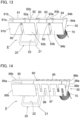
- FIG. 14 is a schematic perspective view of an antenna device according to a ninth embodiment, in which an antenna device 9 includes capacitance loading elements 95 and 96 that have been divided into two in the front-rear direction (longitudinal direction).
- capacitance loading element 95 slanted parts 95b that become chevron-shaped slant faces are respectively formed by bending on both sides of a bottom coupling part 95a so as to include a clearance in an upper part.
- slanted parts 96b that become chevron-shaped slant faces are respectively formed by bending on both sides of a bottom coupling part 96a so as to include a clearance in an upper part, and furthermore, slit-like cutout parts 97 and 98 are alternately formed in upper hems and lower hems of the slanted parts 96b.
- the slanted parts 96b of the capacitance loading element 96 become like a meander (meandering shape).
- the filter 60 mutually connects upper ends of the slanted parts 95b and 96b on the left side of the capacitance loading elements 95 and 96.
- the helical element 70 is connected to the capacitance loading element 96.
- the other configuration is similar to the above-referenced first embodiment, and action effects pursuant to the first embodiment are attained.
- FIG. 15 is a schematic perspective view of an antenna device according to a tenth embodiment, in which an antenna device 10 includes capacitance loading elements 99A and 99B divided into left and right on the rear side of the capacitance loading element 96 illustrated in the ninth embodiment.
- the capacitance loading elements 99A and 99B are like a meander (meandering shape) in which slit-like cutout parts 100 and 101 are alternately formed in upper hems and lower hems.
- the capacitance loading elements 99A and 99B form chevron-shaped slant faces on left and right and are connected to each other via the filter 60 at upper ends of the slanted parts 96b on left and right of the capacitance loading element 96.
- the other configuration is similar to the above-referenced ninth embodiment, and action effects pursuant to the ninth embodiment are attained.
- the position of the helical element 70 corresponding to the component of the antenna 30 for AM/FM broadcast reception is not limited to the front, and the helical element may be connected to the capacitance loading element at the rear position and located in front of the patch antenna 20. Furthermore, the helical element may be offset in the left-right direction orthogonal to the front-rear direction (may be deviated in the left-right direction).
- the position of the filter 60 that mutually connects the capacitance loading elements is not limited to the ends of the capacitance loading elements and may be a position where the capacitance loading elements can be mutually connected, and the number of filters is not limited to 1, and plural pieces may also be used. Furthermore, in a case where it is sufficient when the desired axial ratio is not so low, a configuration may also be adopted in which the respective divided capacitance loading elements are connected by a conductive wire instead of the filter 60.
- the filter 60 is used to mutually connect the respective capacitance loading elements according to the respective embodiments, but a filter that becomes high impedance in the frequency band where the patch antenna 20 operates may be used instead of the filter 60 or together with the filter 60.
- the slit-like cutout parts are formed in both the front edge and the rear edge of the capacitance loading element 44 towards the inward side in the front-rear direction, but improvement effects in the axial ratio are attained also in a case where the slit-like cutout part is formed in only either the front edge or the rear edge.
- the sixth and seventh embodiments illustrate the case where the slit-like cutout parts are provided in a case where the capacitance loading element is divided into two, but there are also cases where the axial ratio may be improved when the slit-like cutout part is provided in a case where the capacitance loading element is not divided and a case where the capacitance loading element is divided into three or more.
- the slit-like cutout parts may be provided in a plurality of capacitance loading elements.
- the capacitance loading element is chevron-shaped having the ridge line, but the configuration is not limited to the chevron shape and may be a flat plate or the like.
Landscapes
- Physics & Mathematics (AREA)
- Electromagnetism (AREA)
- Engineering & Computer Science (AREA)
- Remote Sensing (AREA)
- Waveguide Aerials (AREA)
- Variable-Direction Aerials And Aerial Arrays (AREA)
- Details Of Aerials (AREA)
Abstract
Description
- The present invention relates to an antenna device.
- In a related-art antenna device of this type, to reduce influences of a capacitance loading element on a patch antenna, the capacitance loading element and the patch antenna are arranged so as not to be overlapped with each other as observed from the zenith (above). However, since down-sizing of the antenna device has been demanded in recent years, arrangement of the capacitance loading element above the patch antenna is under review. This case is illustrated in
FIGS. 16A to 16D as a comparative example. - An
antenna device 11 in the comparative example inFIGS. 16A to 16D includes apatch antenna 20 serving as a first antenna mounted on an antenna base that is not illustrated in the drawings and anantenna 30 for AM/FM broadcast reception serving as a second antenna including acapacitance loading element 40 and a helical element (coil) 70. Thecapacitance loading element 40 is an undivided structure continuous in a front-rear direction (longitudinal direction) and is located above thepatch antenna 20. Thepatch antenna 20 is constituted by providing a radiatingelectrode 22 on an upper surface of adielectric substrate 21 arranged on a ground conductor (not illustrated), and a side where theradiating electrode 22 is provided corresponds to an upper side of thepatch antenna 20. InFIG. 16A , front-rear, left-right, and vertical directions are defined. The front-rear direction is a longitudinal direction (direction of a ridge line P) of thecapacitance loading element 40. The left-right direction is a direction orthogonal to the front-rear direction on a horizontal plane, in which a left side corresponds to a left direction when facing the front. The vertical direction is a direction orthogonal to both the front-rear and left-right directions, in which a side where theradiating electrode 22 of thepatch antenna 20 is provided corresponds to an upward direction. - The
capacitance loading element 40 is, for example, a conductive metal plate and is chevron-shaped including slant faces that are lowered towards left and right from the ridge line P at a highest position, in which an angle defined by both slant faces is α = 70°. A length of the capacitance loading element 40 (length in the front-rear direction) is j = 80 mm, and widths of the slant faces on the right side and the left side (lengths along the slant faces in the left-right direction) are k = m = 22.5 mm. A height from the antenna base that is not illustrated in the drawings to the ridge line P is approximately 50 mm, and an interval z between an upper surface of thepatch antenna 20 and a lower end of thecapacitance loading element 40 inFIG. 16C is approximately 24 mm. - When the capacitance loading
element 40 of the undivided structure is simply arranged above thepatch antenna 20 as in the comparative example inFIGS. 16A to 16D , an axial ratio (dB) of thepatch antenna 20 increases to decrease an average gain, and reception performance from broadcast or communication satellites decreases. -
FIG. 17 is a characteristic diagram based on a simulation illustrating a relationship between a frequency (MHz) of the antenna device and an axial ratio at an elevation angle 90° (hereinafter, referred to as an axial ratio) when the capacitance loading element is arranged above the patch antenna as in the comparative example inFIGS. 16A to 16D and when the capacitance loading element is not arranged. As illustrated inFIG. 17 , the axial ratio increases when the capacitance loading element is arranged above the patch antenna (solid line inFIG. 17 ) as compared with a case where the capacitance loading element is not arranged (dotted line inFIG. 17 ). That is, performance of the patch antenna with respect to a circularly polarized wave decreases. Here, it is assumed that the elevation angle indicates an angle from the horizontal plane. - Patent Document 1:
JP-A-2016-32165 -
Patent Document 1 illustrates an antenna device for vehicle that includes a satellite radio antenna and a capacity element (equivalent to a capacitance loading element). The satellite radio antenna is arranged on a front side with respect to the capacity element, and this is an arrangement where the capacity element and the satellite radio antenna are not overlapped with each other as observed from the above. - As described above, when the capacitance loading element is simply arranged above the patch antenna, characteristics of the patch antenna decrease in a case where circularly polarized radio waves from broadcast or communication satellites are transmitted and/or received.
- Embodiments according to the present invention are related to providing a technology for an antenna device with which transmission and/or reception of circularly polarized waves by a patch antenna may be satisfactorily performed irrespective of the presence of a capacitance loading element.
- The present invention is defined by the independent claims. Further aspects of the present invention are defined by the dependent claims.
- A first aspect is an antenna device. This antenna device includes a patch antenna serving as a first antenna, and
- a second antenna including capacitance loading elements,
- the capacitance loading elements being located above the patch antenna and also arranged separately in a predetermined direction.
- It is sufficient when an electrical length in the predetermined direction of each capacitance loading element and an electrical length in a direction orthogonal to the predetermined direction are substantially equal to each other.
- It is sufficient when the capacitance loading elements arranged separately in the predetermined direction are mutually connected by a filter that becomes high impedance in a frequency band where the patch antenna operates.
- It is sufficient when the capacitance loading elements are arranged separately at an equal length in the predetermined direction.
- A second aspect is also an antenna device. This antenna device includes a patch antenna serving as a first antenna, and
- a second antenna including capacitance loading elements,
- the capacitance loading elements being located above the patch antenna, and a slit-like cutout part in a predetermined direction being formed in at least one of side edges of the capacitance loading elements.
- It is sufficient when the capacitance loading elements have a ridge line in the predetermined direction, and slit-like cutout parts are respectively formed on the side edges of the capacitance loading elements in the predetermined direction so as to include an extended line of the ridge line.
- An arbitrary combination of the above-referenced components and expressions of the present invention that has been altered between methods, systems, and the like are also effective as the aspects of the present invention.
- In accordance with the first aspect and the second aspect, in a case where the patch antenna serving as the first antenna and the second antenna including the capacitance loading elements located above the patch antenna are provided, since the capacitance loading elements are arranged separately in the predetermined direction (longitudinal direction) or when the slit-like cutout part in the predetermined direction (longitudinal direction) is formed in at least one of the side edges of the capacitance loading elements, transmission and/or reception of circularly polarized waves by the patch antenna may be satisfactorily performed.
-
-
FIG. 1 is a schematic perspective view illustrating a first embodiment. -
FIG. 2 is a schematic perspective view illustrating a second embodiment. -
FIG. 3 is a schematic perspective view illustrating a third embodiment. -
FIG. 4 is a schematic perspective view illustrating a fourth embodiment. -
FIG. 5 is a schematic perspective view illustrating a fifth embodiment. -
FIG. 6 is a characteristic diagram based on a simulation illustrating a relationship between a frequency and an axial ratio of the antenna device when a capacitance loading element included in an antenna device is divided in a front-rear direction and when the capacitance loading element is not divided. -
FIG. 7 is a characteristic diagram based on a simulation illustrating a relationship between the frequency and an average gain at anelevation angle 10° of the antenna device when the capacitance loading element is divided in the front-rear direction into three and when the capacitance loading element is not divided. -
FIG. 8 is a characteristic diagram based on a simulation illustrating a relationship between the frequency and the axial ratio of the antenna device when the capacitance loading element is equally divided in the front-rear direction and when the capacitance loading element is not equally divided while the number of divided pieces is the same. -
FIG. 9 is a characteristic diagram based on a simulation illustrating a relationship between the frequency of the antenna device and the axial ratio when the capacitance loading element is equally divided in the front-rear direction by different numbers of divisions. -
FIG. 10 is a schematic perspective view illustrating a sixth embodiment. -
FIG. 11 is a schematic perspective view illustrating a seventh embodiment. -
FIG. 12 is a characteristic diagram based on a simulation illustrating a relationship between the frequency and the axial ratio of the antenna device when the capacitance loading element includes a slit-like cutout part and when the capacitance loading element does not include the slit-like cutout part. -
FIG. 13 is a schematic perspective view illustrating an eighth embodiment. -
FIG. 14 is a schematic perspective view illustrating a ninth embodiment. -
FIG. 15 is a schematic perspective view illustrating a tenth embodiment. -
FIG. 16A is a schematic perspective view illustrating a comparative example of the antenna device when the capacitance loading element is not divided in the front-rear direction. -
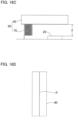
FIG. 16B is a front view when the comparative example is observed from the front. -
FIG. 16C is a side view illustrating a left side when facing the front of the comparative example. -
FIG. 16D is a plane view when the comparative example is observed from the above. -
FIG. 17 is a characteristic diagram based on a simulation illustrating a relationship between the frequency and the axial ratio of the antenna device when the capacitance loading element is arranged above the patch antenna and when the capacitance loading element is not arranged. - Hereinafter, embodiments will be described in detail with reference to the drawings. The same or equivalent components, parts, processes, and the like illustrated in the respective drawings are assigned with the same reference signs, and redundant descriptions will be appropriately omitted. In addition, the embodiments are not intended to limit the present invention and are exemplifications, and all features described in the embodiments and combinations thereof are not necessarily essential to the present invention.
-
FIG. 1 is a schematic perspective view of an antenna device according to a first embodiment, in which anantenna device 1 includes apatch antenna 20 serving as a first antenna mounted on an antenna base that is not illustrated in the drawings and anantenna 30 for AM/FM broadcast reception serving as a second antenna includingcapacitance loading elements patch antenna 20 is a GPS (Global Positioning System) antenna, an SXM (Sirius XM) antenna, a GNSS (Global Navigation Satellite System) antenna, or the like that receives circularly polarized waves from broadcast or communication satellites or transmits circularly polarized waves. Thecapacitance loading elements helical element 70 are components of the antenna for AM/FM broadcast reception. InFIG. 1 , front-rear, left-right, and vertical directions are defined. The front-rear direction is an array direction of thecapacitance loading elements electrode 22 of thepatch antenna 20 is provided corresponds to an upward direction. - The
capacitance loading elements patch antenna 20, and are also arranged by being divided into three in the front-rear direction. Herein, meanings of "above" include not only a case where thepatch antenna 20 is completely overlapped with thecapacitance loading elements antenna device 1 but also a case where part of thepatch antenna 20 is overlapped with thecapacitance loading elements capacitance loading elements filter 60 at ends on a right side when facing the front. A shape and dimensions of thecapacitance loading elements capacitance loading element 40 in the comparative example inFIGS. 16A to 16D . A shape representing clearances between the mutualcapacitance loading elements capacitance loading elements helical element 70 is connected, for example, to thecapacitance loading element 43 at a front position and is located in the front. - The
filter 60 is a filter obtained by connecting a coil and a capacitance in parallel to each other so that parallel resonance occurs (to become high impedance) in an operating frequency band of the patch antenna 20 (for example, a frequency band including 1560 to 1610 MHz illustrated inFIG. 6 or the like), a filter where a self-resonant frequency of the coil is set in the operating frequency band of thepatch antenna 20, or the like. Thefilter 60 connects the dividedcapacitance loading elements capacitance loading elements filter 60 is low impedance in an AM/FM broadcast frequency band, all the dividedcapacitance loading elements helical element 70 in the AM/FM broadcast frequency band. On the other hand, thefilter 60 and thehelical element 70 are high impedance in the operating frequency band of thepatch antenna 20. For this reason, each of the dividedcapacitance loading elements patch antenna 20, and characteristics of thepatch antenna 20 may change. In a case also where thepatch antenna 20 is not overlapped with thecapacitance loading elements capacitance loading elements patch antenna 20, the characteristics of thepatch antenna 20 may change. - For reduction in height of the
antenna device 1, the intervals between an upper surface of the patch antenna 20 (the radiating electrode 22) and lower ends of thecapacitance loading elements patch antenna 20 is set as λ, the intervals between the upper surface of thepatch antenna 20 and the lower ends of thecapacitance loading elements -
FIG. 2 is a schematic perspective view of an antenna device according to a second embodiment, in which anantenna device 2 includescapacitance loading elements capacitance loading elements capacitance loading element 40 in the comparative example inFIGS. 16A to 16D . Thehelical element 70 is connected, for example, to thecapacitance loading element 45 in a front position. The other configuration is similar to the above-referenced first embodiment. -
FIG. 6 is a characteristic diagram based on a simulation illustrating a relationship between a frequency (MHz) and an axial ratio (dB) of the antenna device when the capacitance loading element is divided in the front-rear direction (the first embodiment inFIG. 1 or the second embodiment inFIG. 2 ) and when the capacitance loading element is not divided (the comparative example inFIGS. 16A to 16D ). From this diagram, the axial ratio considerably decreases in the second embodiment corresponding to the division into two as compared with the case of the comparative example in which the capacitance loading element is not divided, and the axial ratio further decreases in the first embodiment corresponding to the division into three. -
FIG. 7 is a characteristic diagram based on a simulation illustrating a relationship between the frequency (MHz) and an average gain (dBi) of the antenna device upon circularly polarized wave reception at anelevation angle 10° when the capacitance loading element is divided into three in the front-rear direction (the first embodiment inFIG. 1 ) and when the capacitance loading element is not divided (the comparative example inFIGS. 16A to 16D ). It is understood from this diagram that the average gain increases in the first embodiment corresponding to the division into three as compared with the case of the comparative example in which the capacitance loading element is not divided. - In the characteristic diagrams in
FIG. 6 andFIG. 7 , when lengths of thecapacitance loading elements FIG. 1 and thecapacitance loading elements FIG. 2 in the front-rear direction are set as a, b, c, f, and h, a length along slant faces on the right side with respect to the ridge line P is set as d, and a length along slant faces on the left side is set as e, a = 35 mm, b = 21 mm, c = 20 mm, f = 45 mm, h = 33 mm are established, and d = e = 22.5 mm (same for all the respectivecapacitance loading elements capacitance loading elements capacitance loading elements capacitance loading elements 41 to 45 is the same as thecapacitance loading element 40 inFIGS. 16A to 16D . As understood from the relationships among the dimensions a, b, c, f, and h, according to the first embodiment inFIG. 1 and the second embodiment inFIG. 2 , the capacitance loading element is not divided at equal lengths in the front-rear direction (not equally divided). - When the capacitance loading element is divided in the front-rear direction as in the first embodiment and the second embodiment, a difference between an electrical length in each of the divided
capacitance loading elements capacitance loading elements FIG. 6 . In addition, when the electrical length in each of the divided capacitance loading elements in the front-rear direction becomes shorter than a wavelength in the operating frequency band of thepatch antenna 20, influences caused by the capacitance loading elements located above thepatch antenna 20 on antenna characteristics of thepatch antenna 20 are reduced. For this reason, as illustrated inFIG. 7 , when the capacitance loading element is divided into three in the front-rear direction, the average gain at a low elevation angle (elevation angle 10°) improves as compared with a case where the capacitance loading element is not divided. When the number of divisions of the capacitance loading element is increased, since the number offilters 60 is increased to increase costs, the number of divisions of the capacitance loading element is desirably set as approximately 3 in a case where the capacitance loading element is not equally divided. In addition, intervals between the upper surface of the patch antenna 20 (radiating electrode 22) and lower ends of thecapacitance loading elements - In accordance with the above-referenced first embodiment, the following effects may be realized.
- (1) In a case where the
patch antenna 20 serving as the first antenna and theantenna 30 for AM/FM broadcast reception serving as the second antenna are provided, thecapacitance loading elements antenna 30 for AM/FM broadcast reception. For this reason, the axial ratio with respect to the circularly polarized waves may be decreased as compared with the capacitance loading element of the undivided structure. As a result, transmission and/or reception of circularly polarized waves may be satisfactorily performed by thepatch antenna 20 irrespective of the presence of thecapacitance loading elements patch antenna 20. - (2) In addition, because of the
capacitance loading elements patch antenna 20 at the low elevation angle may be satisfactorily maintained as compared with the capacitance loading element of the undivided structure. - (3) The
capacitance loading elements capacitance loading elements filter 60 that become high impedance in the frequency band where thepatch antenna 20 operates. Thus, thecapacitance loading elements patch antenna 20, and it is possible to abbreviate adverse influences on the patch antenna 20 (decrease in the average gain). - In accordance with the second embodiment, since the
capacitance loading elements 44 and 45 (structure of the capacitance loading element divided into two) arranged separately in the predetermined direction (front-rear direction) are used as the components of theantenna 30 for AM/FM broadcast reception, action effects pursuant to the first embodiment may be attained. -
FIG. 3 is a schematic perspective view of an antenna device according to a third embodiment, in which anantenna device 3 includescapacitance loading elements capacitance loading elements capacitance loading element 40 in the comparative example inFIGS. 16A to 16D . Thehelical element 70 is connected, for example, to thecapacitance loading element 48 at a front position. The other configuration is similar to the above-referenced first embodiment. -
FIG. 4 is a schematic perspective view of an antenna device according to a fourth embodiment, in which anantenna device 4 includescapacitance loading elements capacitance loading elements capacitance loading element 40 in the comparative example inFIGS. 16A to 16D . Thehelical element 70 is connected, for example, to thecapacitance loading element 54 at a front position. The other configuration is similar to the above-referenced first embodiment. -
FIG. 5 is a schematic perspective view of an antenna device according to a fifth embodiment, in which anantenna device 5 includescapacitance loading elements capacitance loading elements capacitance loading element 40 in the comparative example inFIGS. 16A to 16D . Thehelical element 70 is connected, for example, to thecapacitance loading element 59 at a front position. The other configuration is similar to the above-referenced first embodiment. -
FIG. 8 is a characteristic diagram based on a simulation illustrating a relationship between the frequency (MHz) and the axial ratio (dB) of the antenna device when the capacitance loading element is equally divided in the front-rear direction (divided into three) (third embodiment inFIG. 3 ) and when capacitance loading element is not equally divided while the number of divided pieces is the same (the first embodiment inFIG. 1 ). When thecapacitance loading elements capacitance loading elements capacitance loading elements capacitance loading elements FIG. 8 , when thecapacitance loading elements -
FIG. 9 is a characteristic diagram based on a simulation illustrating a relationship between the frequency (MHz) and the axial ratio (dB) of the antenna device when the capacitance loading element is equally divided in the front-rear direction by different numbers of divisions (3 to 5). When thecapacitance loading elements FIG. 4 to set the difference between the electrical length in the front-rear direction and the electrical length in the left-right direction of each of thecapacitance loading elements FIG. 3 where the capacitance loading element is equally divided into three in the front-rear direction or the fifth embodiment inFIG. 5 where the capacitance loading element is equally divided into five). In a case where physical lengths are the same, an electrical length in a direction including a bent part or a warped part of the capacitance loading element becomes shorter than an electrical length in a flat direction. For this reason, the length of each of thecapacitance loading elements capacitance loading elements FIG. 4 . - In a case where the length of each of the divided capacitance loading elements in the left-right direction varies or a case where the angle defined by the slant faces on both sides of the ridge line changes, it is sufficient when the difference between the electrical length in the front-rear direction and the electrical length in the left-right direction is set to be small with regard to each of the capacitance loading elements.
- <Sixth Embodiment>
-
FIG. 10 is a schematic perspective view of an antenna device according to a sixth embodiment, in which anantenna device 6 is obtained by forming a pair of slit-like cutout parts 80 in thecapacitance loading element 44 that has the longer length in the front-rear direction among thecapacitance loading elements capacitance loading element 44 has the ridge line P in the front-rear direction, and so as to include an extended line of the ridge line P in side edges (a front edge and a rear edge) on both sides of thecapacitance loading element 44 in the front-rear direction, the slit-like cutout parts 80 are respectively formed from the side edges towards an inward side (the slit-like cutout part 80 is formed from the front edge of thecapacitance loading element 44 towards the rear, and the slit-like cutout part 80 is formed from the rear edge of thecapacitance loading element 44 towards the front). A shape and dimensions of thecapacitance loading elements capacitance loading element 40 in the comparative example inFIGS. 16A to 16D . The other configuration is similar to the above-referenced second embodiment. -
FIG. 11 is a schematic perspective view of an antenna device according to a seventh embodiment, in which anantenna device 7 is obtained by forming a pair of slit-like cutout parts 81 in the side edges (the front edge and the rear edge) on both sides in the front-rear direction of thecapacitance loading element 44 that has the longer length in the front-rear direction (longitudinal direction), and the positions of the slit-like cutout parts 81 are positions out of the ridge line P of the capacitance loading element 44 (slant face on the right side). A shape and dimensions of thecapacitance loading elements capacitance loading element 40 in the comparative example inFIGS. 16A to 16D . The other configuration is similar to the above-referenced second embodiment. A configuration may also be adopted in which one of the slit-like cutout parts 81 is arranged on the left side of thecapacitance loading element 44, and the other one of the slit-like cutout parts 81 is arranged on the right side. -
FIG. 12 is a characteristic diagram based on a simulation illustrating a relationship between the frequency (MHz) and the axial ratio (dB) in the case of theantenna device 6 of the sixth embodiment in which thecapacitance loading element 44 has the slit-like cutout parts 80 and the case of theantenna device 7 of the seventh embodiment in which thecapacitance loading element 44 has the slit-like cutout parts 81 in contrast with a case where the capacitance loading element does not have the slit-like cutout parts (equivalent to the second embodiment where the capacitance loading element is divided into two). Thecapacitance loading element 44 has the slit-like cutout parts 80 or the slit-like cutout parts 81 that are formed by being cut out from the side edges on both sides in the front-rear direction (in other words, the side edges along the left-right direction) towards the inward side. Thus, the electrical length along the side edge of thecapacitance loading element 44 in the left-right direction may be increased, and the difference between the electrical length in the left-right direction and the electrical length in the front-rear direction of thecapacitance loading element 44 is decreased. For this reason, in the case of the sixth and seventh embodiments in which the slit-like cutout parts FIG. 11 , the slit-like cutout parts 81 are located only on the right side of thecapacitance loading element 44. When the slit-like cutout parts 81 do not exist in the above (in the vicinity of the position of the ridge line P) in this manner, the difference between the electrical lengths in the left-right direction and the front-rear direction of thecapacitance loading element 44 is not decreased as compared with a case where the slit-like cutout parts 80 exist in the above as in the sixth embodiment inFIG. 10 . For this reason, as illustrated inFIG. 12 , the axial ratio is not decreased in the case of the seventh embodiment as much as the sixth embodiment. - In the case of the capacitance loading elements that have been divided into two in
FIG. 10 and FIG. 11 , since the electrical length in the front-rear direction of the capacitance loading element is longer than the electrical length in the left-right direction of the capacitance loading element, for example, provision of the slit-like cutout parts in thecapacitance loading element 44 in the left-right direction (the electrical length of thecapacitance loading element 44 in the front-rear direction is further increased) leads to increase in the axial ratio, which is not preferable. -
FIG. 13 is a schematic perspective view of an antenna device according to an eighth embodiment, in which anantenna device 8 includescapacitance loading elements capacitance loading elements slanted parts bottom coupling parts parts filter 60 are provided between upper ends on the right side of the slantedparts parts filter 60 is provided between upper ends on the left side of the slantedparts helical element 70 is connected to thecapacitance loading element 94. The other configuration is similar to the above-referenced fourth embodiment. - In accordance with the eighth embodiment, when the
capacitance loading elements -
FIG. 14 is a schematic perspective view of an antenna device according to a ninth embodiment, in which anantenna device 9 includescapacitance loading elements capacitance loading element 95, slantedparts 95b that become chevron-shaped slant faces are respectively formed by bending on both sides of abottom coupling part 95a so as to include a clearance in an upper part. In thecapacitance loading element 96, slantedparts 96b that become chevron-shaped slant faces are respectively formed by bending on both sides of abottom coupling part 96a so as to include a clearance in an upper part, and furthermore, slit-like cutout parts parts 96b. As a result, the slantedparts 96b of thecapacitance loading element 96 become like a meander (meandering shape). Thefilter 60 mutually connects upper ends of the slantedparts capacitance loading elements helical element 70 is connected to thecapacitance loading element 96. The other configuration is similar to the above-referenced first embodiment, and action effects pursuant to the first embodiment are attained. -
FIG. 15 is a schematic perspective view of an antenna device according to a tenth embodiment, in which anantenna device 10 includescapacitance loading elements capacitance loading element 96 illustrated in the ninth embodiment. Thecapacitance loading elements like cutout parts capacitance loading elements filter 60 at upper ends of the slantedparts 96b on left and right of thecapacitance loading element 96. The other configuration is similar to the above-referenced ninth embodiment, and action effects pursuant to the ninth embodiment are attained. - A plurality of embodiments have been described above, but various modifications of the respective components and the respective processing processes of the respective embodiments may be made. For example, the following modified examples are considerable.
- In the respective embodiments, the position of the
helical element 70 corresponding to the component of theantenna 30 for AM/FM broadcast reception is not limited to the front, and the helical element may be connected to the capacitance loading element at the rear position and located in front of thepatch antenna 20. Furthermore, the helical element may be offset in the left-right direction orthogonal to the front-rear direction (may be deviated in the left-right direction). - In the respective embodiments, the position of the
filter 60 that mutually connects the capacitance loading elements is not limited to the ends of the capacitance loading elements and may be a position where the capacitance loading elements can be mutually connected, and the number of filters is not limited to 1, and plural pieces may also be used. Furthermore, in a case where it is sufficient when the desired axial ratio is not so low, a configuration may also be adopted in which the respective divided capacitance loading elements are connected by a conductive wire instead of thefilter 60. - The
filter 60 is used to mutually connect the respective capacitance loading elements according to the respective embodiments, but a filter that becomes high impedance in the frequency band where thepatch antenna 20 operates may be used instead of thefilter 60 or together with thefilter 60. - In the sixth embodiment in
FIG. 10 and the seventh embodiment inFIG. 11 , the slit-like cutout parts are formed in both the front edge and the rear edge of thecapacitance loading element 44 towards the inward side in the front-rear direction, but improvement effects in the axial ratio are attained also in a case where the slit-like cutout part is formed in only either the front edge or the rear edge. The sixth and seventh embodiments illustrate the case where the slit-like cutout parts are provided in a case where the capacitance loading element is divided into two, but there are also cases where the axial ratio may be improved when the slit-like cutout part is provided in a case where the capacitance loading element is not divided and a case where the capacitance loading element is divided into three or more. In addition, the slit-like cutout parts may be provided in a plurality of capacitance loading elements. - According to the respective embodiments, the case has been exemplified where the capacitance loading element is chevron-shaped having the ridge line, but the configuration is not limited to the chevron shape and may be a flat plate or the like.
-
- 1 TO 11 ANTENNA DEVICE
- 20 PATCH ANTENNA
- 30 ANTENNA FOR AM/FM BROADCAST RECEPTION
- 40 TO 48, 51 TO 59 CAPACITANCE LOADING ELEMENT
- 60 FILTER
- 70 HELICAL ELEMENT
- 80, 81 SLIT-LIKE CUTOUT PART
- The following are preferred aspects of the present invention:
- 1. An antenna device comprising:
- a patch antenna serving as a first antenna; and
- a second antenna including capacitance loading elements,
- the capacitance loading elements being located above the patch antenna and also arranged separately in a predetermined direction.
- 2. The antenna device according to1, wherein an electrical length of each of the capacitance loading elements in the predetermined direction and an electrical length in a direction orthogonal to the predetermined direction are substantially equal to each other.
- 3. The antenna device according to 1 or 2, wherein the capacitance loading elements arranged separately in the predetermined direction are mutually connected by a filter that becomes high impedance in a frequency band where the patch antenna operates.
- 4. The antenna device according to any one of1 to 3, wherein the capacitance loading elements are arranged separately at an equal length in the predetermined direction.
- 5. An antenna device comprising:
- a patch antenna serving as a first antenna; and
- a second antenna including capacitance loading elements,
- the capacitance loading elements being located above the patch antenna, and a slit-like cutout part in a predetermined direction being formed in at least one of side edges of the capacitance loading elements.
- 6. The antenna device according to 5, wherein the capacitance loading elements have a ridge line in the predetermined direction, and slit-like cutout parts are respectively formed on the side edges of the capacitance loading elements in the predetermined direction so as to include an extended line of the ridge line.
Claims (9)
- An antenna device, comprising:a first antenna that operates in a first frequency band; anda second antenna that operates in a second frequency band different from the first frequency band, whereinthe second antenna includes a capacitance loading element having a part which is overlapped with the first antenna when observed from above of the antenna device, anda slit-like cutout part is formed in the capacitance loading element.
- The antenna device according to the claim 1, wherein
the capacitance loading element has a meandering shape in which slit-like cutout parts are alternately formed. - The antenna device according to the claim 1 or 2, whereinthe capacitance loading element has at least two divided bodies, andat least one of the divided bodies is formed with the slit-like cutout part.
- The antenna device according to the claim 3, wherein
the divided bodies are mutually connected by a filter or a conductive wire. - The antenna device according to the claim 4, wherein
the filter or the conductive wire becomes high impedance in the first frequency band. - The antenna device according to any one of the claims 1 to 5, whereinthe first antenna is a patch antenna, andthe slit-like cutout part is disposed so as to be overlapped with at least a part of the patch antenna when observed from side of the antenna device.
- The antenna device according to the claim 6, wherein
an interval between a radiation surface of the patch antenna and a lower end of the capacitance loading element when observed from side of the antenna device is shorter than 0.25 times of a wavelength of the first frequency band. - The antenna device according to any one of the claims 1 to 7, whereinthe capacitance loading element has a chevron shape when observed from a front side or a rear side of the antenna device,the capacitance loading element has a first slant face and a second slant face which form the chevron shape, andan upper edge of the first slant face and an upper edge of the second slant face are mutually separated.
- The antenna device according to any one of the claims 1 to 8, whereinthe first antenna is an antenna for a satellite, andthe second antenna is an antenna for a radio broadcasting.
Applications Claiming Priority (3)
| Application Number | Priority Date | Filing Date | Title |
|---|---|---|---|
| JP2017037653 | 2017-02-28 | ||
| PCT/JP2018/007479 WO2018159668A1 (en) | 2017-02-28 | 2018-02-28 | Antenna device |
| EP18760255.2A EP3591762B1 (en) | 2017-02-28 | 2018-02-28 | Antenna device |
Related Parent Applications (2)
| Application Number | Title | Priority Date | Filing Date |
|---|---|---|---|
| EP18760255.2A Division-Into EP3591762B1 (en) | 2017-02-28 | 2018-02-28 | Antenna device |
| EP18760255.2A Division EP3591762B1 (en) | 2017-02-28 | 2018-02-28 | Antenna device |
Publications (1)
| Publication Number | Publication Date |
|---|---|
| EP4178038A1 true EP4178038A1 (en) | 2023-05-10 |
Family
ID=63370356
Family Applications (2)
| Application Number | Title | Priority Date | Filing Date |
|---|---|---|---|
| EP18760255.2A Active EP3591762B1 (en) | 2017-02-28 | 2018-02-28 | Antenna device |
| EP22213944.6A Pending EP4178038A1 (en) | 2017-02-28 | 2018-02-28 | Antenna device |
Family Applications Before (1)
| Application Number | Title | Priority Date | Filing Date |
|---|---|---|---|
| EP18760255.2A Active EP3591762B1 (en) | 2017-02-28 | 2018-02-28 | Antenna device |
Country Status (5)
| Country | Link |
|---|---|
| US (2) | US11251528B2 (en) |
| EP (2) | EP3591762B1 (en) |
| JP (3) | JP6683885B2 (en) |
| CN (3) | CN110337757B (en) |
| WO (1) | WO2018159668A1 (en) |
Families Citing this family (4)
| Publication number | Priority date | Publication date | Assignee | Title |
|---|---|---|---|---|
| JP6956650B2 (en) * | 2018-02-19 | 2021-11-02 | 株式会社ヨコオ | Automotive antenna device |
| JP7368134B2 (en) | 2019-07-26 | 2023-10-24 | 株式会社ヨコオ | antenna device |
| JP7734687B2 (en) * | 2020-11-16 | 2025-09-05 | 株式会社ヨコオ | antenna |
| CN117083769A (en) * | 2021-03-29 | 2023-11-17 | 株式会社友华 | Vehicle-mounted antenna device |
Citations (5)
| Publication number | Priority date | Publication date | Assignee | Title |
|---|---|---|---|---|
| US20120026050A1 (en) * | 2010-07-30 | 2012-02-02 | Takeshi Sampo | Antenna Device |
| US20120326935A1 (en) * | 2011-06-23 | 2012-12-27 | Winnercom Co., Ltd. | Broadcasting antenna for vehicle and shark fin antenna apparatus having the same |
| US20130176180A1 (en) * | 2008-07-11 | 2013-07-11 | Harada Industry Co., Ltd. | Antenna apparatus |
| US20150200446A1 (en) * | 2011-03-24 | 2015-07-16 | Harada Industry Co., Ltd. | Antenna device |
| JP2016032165A (en) | 2014-07-28 | 2016-03-07 | 株式会社ヨコオ | In-vehicle antenna device |
Family Cites Families (28)
| Publication number | Priority date | Publication date | Assignee | Title |
|---|---|---|---|---|
| US5402134A (en) * | 1993-03-01 | 1995-03-28 | R. A. Miller Industries, Inc. | Flat plate antenna module |
| US5778306A (en) * | 1996-11-08 | 1998-07-07 | Motorola Inc. | Low loss high frequency transmitting/receiving switching module |
| US6114996A (en) * | 1997-03-31 | 2000-09-05 | Qualcomm Incorporated | Increased bandwidth patch antenna |
| US6603430B1 (en) * | 2000-03-09 | 2003-08-05 | Tyco Electronics Logistics Ag | Handheld wireless communication devices with antenna having parasitic element |
| JP2002094323A (en) * | 2000-09-20 | 2002-03-29 | Murata Mfg Co Ltd | Circularly polarized wave antenna system |
| SE519727C2 (en) * | 2000-12-29 | 2003-04-01 | Allgon Mobile Comm Ab | Antenna device for use in at least two frequency bands |
| JP3868775B2 (en) * | 2001-02-23 | 2007-01-17 | 宇部興産株式会社 | ANTENNA DEVICE AND COMMUNICATION DEVICE USING THE SAME |
| DE60223515T2 (en) * | 2001-03-15 | 2008-09-18 | Matsushita Electric Industrial Co., Ltd., Kadoma | ANTENNA DEVICE |
| US6518934B1 (en) * | 2001-10-29 | 2003-02-11 | Northrop Grumman Corporation | Parasitically driven dipole array |
| JP4381269B2 (en) * | 2004-09-27 | 2009-12-09 | 三洋電機株式会社 | Semiconductor integrated circuit device |
| JP5105208B2 (en) * | 2007-05-17 | 2012-12-26 | 株式会社村田製作所 | ANTENNA DEVICE AND RADIO COMMUNICATION DEVICE |
| US20080303633A1 (en) * | 2007-06-07 | 2008-12-11 | The Hong Kong University Of Science And Technology | High gain rfid tag antennas |
| US20100156600A1 (en) * | 2008-12-19 | 2010-06-24 | Mark Duron | Method and System for a Broadband Impedance Compensated Slot Antenna (BICSA) |
| US20100231461A1 (en) * | 2009-03-13 | 2010-09-16 | Qualcomm Incorporated | Frequency selective multi-band antenna for wireless communication devices |
| WO2010150403A1 (en) * | 2009-06-26 | 2010-12-29 | 三菱電機株式会社 | Wireless communication device |
| WO2011105380A1 (en) * | 2010-02-24 | 2011-09-01 | シャープ株式会社 | Antenna and portable wireless terminal |
| JP2012054915A (en) * | 2010-08-06 | 2012-03-15 | Nippon Soken Inc | Antenna structure and diversity antenna structure |
| US8537062B1 (en) * | 2010-09-30 | 2013-09-17 | Laird Technologies, Inc. | Low-profile antenna assemblies |
| JP2013110601A (en) * | 2011-11-21 | 2013-06-06 | Furukawa Electric Co Ltd:The | On-vehicle antenna device |
| CN202651349U (en) * | 2012-04-20 | 2013-01-02 | 卜放 | Umbrella-shaped antenna oscillator |
| US9595752B2 (en) * | 2012-11-02 | 2017-03-14 | Harada Industry Co., Ltd. | Vehicle antenna unit |
| US9325354B2 (en) * | 2013-11-20 | 2016-04-26 | Intel Corporation | Wideband frequency shift modulation using transient state of antenna |
| WO2016005909A1 (en) * | 2014-07-07 | 2016-01-14 | University Of Manitoba | Imaging using reconfigurable antennas |
| KR101633844B1 (en) * | 2014-10-14 | 2016-06-28 | 위너콤 주식회사 | Multi-Band Antenna for Vehicle |
| JP5918844B2 (en) * | 2014-12-22 | 2016-05-18 | 原田工業株式会社 | Antenna device |
| CN104868227A (en) * | 2015-04-03 | 2015-08-26 | 卜放 | Combined antenna oscillator, dwarf type vehicle-mounted antenna and method for manufacturing combined antenna oscillator |
| JP6336422B2 (en) * | 2015-09-29 | 2018-06-06 | 原田工業株式会社 | Antenna device |
| CN110024220B (en) * | 2016-12-06 | 2022-03-11 | 株式会社友华 | Antenna device |
-
2018
- 2018-02-28 EP EP18760255.2A patent/EP3591762B1/en active Active
- 2018-02-28 JP JP2019503055A patent/JP6683885B2/en active Active
- 2018-02-28 WO PCT/JP2018/007479 patent/WO2018159668A1/en not_active Ceased
- 2018-02-28 CN CN201880014209.XA patent/CN110337757B/en active Active
- 2018-02-28 EP EP22213944.6A patent/EP4178038A1/en active Pending
- 2018-02-28 CN CN202310406241.5A patent/CN116387835A/en active Pending
- 2018-02-28 US US16/487,096 patent/US11251528B2/en active Active
- 2018-02-28 CN CN202110409967.5A patent/CN113131180B/en active Active
-
2020
- 2020-03-26 JP JP2020055667A patent/JP7216041B2/en active Active
-
2022
- 2022-01-05 US US17/568,725 patent/US11888241B2/en active Active
-
2023
- 2023-01-18 JP JP2023005852A patent/JP7539508B2/en active Active
Patent Citations (5)
| Publication number | Priority date | Publication date | Assignee | Title |
|---|---|---|---|---|
| US20130176180A1 (en) * | 2008-07-11 | 2013-07-11 | Harada Industry Co., Ltd. | Antenna apparatus |
| US20120026050A1 (en) * | 2010-07-30 | 2012-02-02 | Takeshi Sampo | Antenna Device |
| US20150200446A1 (en) * | 2011-03-24 | 2015-07-16 | Harada Industry Co., Ltd. | Antenna device |
| US20120326935A1 (en) * | 2011-06-23 | 2012-12-27 | Winnercom Co., Ltd. | Broadcasting antenna for vehicle and shark fin antenna apparatus having the same |
| JP2016032165A (en) | 2014-07-28 | 2016-03-07 | 株式会社ヨコオ | In-vehicle antenna device |
Also Published As
| Publication number | Publication date |
|---|---|
| CN110337757B (en) | 2023-07-25 |
| US20210135363A1 (en) | 2021-05-06 |
| JP7216041B2 (en) | 2023-01-31 |
| US20220131272A1 (en) | 2022-04-28 |
| WO2018159668A1 (en) | 2018-09-07 |
| JP6683885B2 (en) | 2020-04-22 |
| EP3591762A1 (en) | 2020-01-08 |
| EP3591762B1 (en) | 2023-02-15 |
| EP3591762A4 (en) | 2020-05-27 |
| US11251528B2 (en) | 2022-02-15 |
| CN116387835A (en) | 2023-07-04 |
| JP2020096390A (en) | 2020-06-18 |
| JP7539508B2 (en) | 2024-08-23 |
| CN110337757A (en) | 2019-10-15 |
| JPWO2018159668A1 (en) | 2019-12-26 |
| US11888241B2 (en) | 2024-01-30 |
| JP2023033550A (en) | 2023-03-10 |
| CN113131180A (en) | 2021-07-16 |
| CN113131180B (en) | 2024-07-30 |
Similar Documents
| Publication | Publication Date | Title |
|---|---|---|
| US11888241B2 (en) | Antenna device | |
| EP2826097B1 (en) | Phased array antenna | |
| US11177583B2 (en) | Electronic device and antenna structure thereof | |
| US20100182203A1 (en) | Broadband antenna for wireless communications | |
| EP2908380A1 (en) | Wideband dual-polarized patch antenna array and methods useful in conjunction therewith | |
| WO2019064470A1 (en) | Antenna device | |
| EP3691035A1 (en) | Patch antenna and antenna device | |
| US9614292B2 (en) | Circularly polarized antenna | |
| CN101533949B (en) | Small conformable broadband traveling-wave antennas on platform | |
| CN116780175B (en) | Broadband millimeter wave end-fire antenna | |
| US8106841B2 (en) | Antenna structure | |
| WO2021040892A1 (en) | Base station antennas having low cost wideband cross-dipole radiating elements | |
| EP3958398B1 (en) | Dual band omnidirectional antenna | |
| CN105633586A (en) | Antenna device and electronic device | |
| US20240421494A1 (en) | Base station antennas having compact dual-polarized box dipole radiating elements therein that support high band cloaking | |
| EP4064455A1 (en) | Microstrip antenna and information device | |
| CN102025029B (en) | Antenna | |
| CN113206382A (en) | Feed antenna unit for automobile navigation | |
| JP3038205B1 (en) | Waveguide-fed planar antenna | |
| JP4254831B2 (en) | Antenna device | |
| CN108511907B (en) | Antenna system and communication terminal | |
| Shinde et al. | Circularly Polarized Meandered Rotated Square Microstrip Antenna for Multiband Applications | |
| CN116487892A (en) | waveguide slot antenna array | |
| JPH0884018A (en) | Electromagnetic coupling patch antenna |
Legal Events
| Date | Code | Title | Description |
|---|---|---|---|
| PUAI | Public reference made under article 153(3) epc to a published international application that has entered the european phase |
Free format text: ORIGINAL CODE: 0009012 |
|
| STAA | Information on the status of an ep patent application or granted ep patent |
Free format text: STATUS: REQUEST FOR EXAMINATION WAS MADE |
|
| 17P | Request for examination filed |
Effective date: 20221215 |
|
| AC | Divisional application: reference to earlier application |
Ref document number: 3591762 Country of ref document: EP Kind code of ref document: P |
|
| AK | Designated contracting states |
Kind code of ref document: A1 Designated state(s): AL AT BE BG CH CY CZ DE DK EE ES FI FR GB GR HR HU IE IS IT LI LT LU LV MC MK MT NL NO PL PT RO RS SE SI SK SM TR |
|
| STAA | Information on the status of an ep patent application or granted ep patent |
Free format text: STATUS: EXAMINATION IS IN PROGRESS |
|
| 17Q | First examination report despatched |
Effective date: 20260305 |