EP4177786A1 - Electronic integrator circuit for driving inductor - Google Patents
Electronic integrator circuit for driving inductor Download PDFInfo
- Publication number
- EP4177786A1 EP4177786A1 EP21306564.2A EP21306564A EP4177786A1 EP 4177786 A1 EP4177786 A1 EP 4177786A1 EP 21306564 A EP21306564 A EP 21306564A EP 4177786 A1 EP4177786 A1 EP 4177786A1
- Authority
- EP
- European Patent Office
- Prior art keywords
- current
- voltage
- integrator input
- driver
- integrator
- Prior art date
- Legal status (The legal status is an assumption and is not a legal conclusion. Google has not performed a legal analysis and makes no representation as to the accuracy of the status listed.)
- Granted
Links
Images




Classifications
-
- G—PHYSICS
- G06—COMPUTING OR CALCULATING; COUNTING
- G06G—ANALOGUE COMPUTERS
- G06G7/00—Devices in which the computing operation is performed by varying electric or magnetic quantities
- G06G7/12—Arrangements for performing computing operations, e.g. operational amplifiers specially adapted therefor
- G06G7/18—Arrangements for performing computing operations, e.g. operational amplifiers specially adapted therefor for integration or differentiation; for forming integrals
- G06G7/184—Arrangements for performing computing operations, e.g. operational amplifiers specially adapted therefor for integration or differentiation; for forming integrals using capacitive elements
-
- H—ELECTRICITY
- H03—ELECTRONIC CIRCUITRY
- H03K—PULSE TECHNIQUE
- H03K4/00—Generating pulses having essentially a finite slope or stepped portions
- H03K4/06—Generating pulses having essentially a finite slope or stepped portions having triangular shape
- H03K4/08—Generating pulses having essentially a finite slope or stepped portions having triangular shape having sawtooth shape
- H03K4/48—Generating pulses having essentially a finite slope or stepped portions having triangular shape having sawtooth shape using as active elements semiconductor devices
- H03K4/50—Generating pulses having essentially a finite slope or stepped portions having triangular shape having sawtooth shape using as active elements semiconductor devices in which a sawtooth voltage is produced across a capacitor
-
- H—ELECTRICITY
- H03—ELECTRONIC CIRCUITRY
- H03K—PULSE TECHNIQUE
- H03K17/00—Electronic switching or gating, i.e. not by contact-making and –breaking
- H03K17/51—Electronic switching or gating, i.e. not by contact-making and –breaking characterised by the components used
- H03K17/56—Electronic switching or gating, i.e. not by contact-making and –breaking characterised by the components used by the use, as active elements, of semiconductor devices
- H03K17/687—Electronic switching or gating, i.e. not by contact-making and –breaking characterised by the components used by the use, as active elements, of semiconductor devices the devices being field-effect transistors
- H03K17/6871—Electronic switching or gating, i.e. not by contact-making and –breaking characterised by the components used by the use, as active elements, of semiconductor devices the devices being field-effect transistors the output circuit comprising more than one controlled field-effect transistor
Definitions
- the present disclosure relates generally to electronic integration circuits, and more specifically, to an integrator that drives an inductive coil or the like.
- a conventional integrator circuit includes an operational amplifier that provides a desired current response, wave shape, or other signal conditioning functions.
- the presence of an amplifier in an integrator circuit may operate under strict time and peak current conditions, which prohibits the circuit from achieving a combination of ideal characteristics in order to integrate a linear current ramp necessary for driving the integrator input.
- a simple integrator circuit for example, comprising few transistors including a follower stage, that is capable of driving a high peak current rise, e.g., 130mA, in a coil in 6ns or less.
- embodiments of the present inventive concept include a simple integrator circuit that can drive a small inductor with an integrator amplifier that generates a quadratic shape pulse based on the integration of a linear ramp current.
- the integrator circuit operates under strict and tight parameters, in particular, providing a bias current to maintain the integrator input at the same voltage with little or no input current with respect to a small inductor, where the signals having a predetermined longer pulse duration (e.g., 6ns compared to conventional 2ns or 4ns pulse durations) and high peak current (e.g., 150mA).
- the integrator can be implemented in various electronic applications including, but by no means limited to, automotive, industrial, and consumer applications.
- One example application may include a 10Mbit/s isolated communication bus for a battery management system (BMS), which requires the integrator to drive a 30nH inductive load requiring a pulse producing a 130mA current in 6ns.
- BMS battery management system
- Other high speed isolated communication network electronic circuits may equally apply, for example, a microcontroller, battery cell controller, transceiver, and so on.
- FIG. 1 is a block diagram of an integrator circuit 100 of a communication bus 10, in accordance with some embodiments.
- the integrator circuit 100 can be implemented in various electronic applications including, but by no means limited to, automotive, industrial, and consumer applications including signal processing or battery management systems.
- One application includes the implementation of a computer chip or related electronic integration circuit for a communication bus.
- the integrator circuit 100 can comprise a first stage driver 102, an integrator input element 104, an inductive load driver 106, and an integrator capacitor 108.
- one or more of the first stage driver 102, the integrator input element 104, and the inductive load driver 106 can be formed of Metal-Oxide-Semiconductor Field-Effect Transistors (MOSFETs), and preferably NMOS transistors, but not limited thereto.
- MOSFETs Metal-Oxide-Semiconductor Field-Effect Transistors
- the inductive load driver 106 can be constructed and arranged to drive an inductive load such as a coil 110 as a voltage follower stage.
- the inductive load driver 106 can have a source coupled to both the integrator capacitor 108 and the coil 110.
- the capacitor 108 can be coupled to the conductive path between the inductive load driver 106 and the coil 110.
- the inductive load driver 106 further has a drain and gate each coupled to a current source 122, for example, a 2mA current source.
- the first stage driver 102 can be constructed and arranged to drive the follower stage via the drain of the first stage driver 102, which can be in electrical communication with the gate of the inductive load driver 106.
- the first stage driver 102 can be formed of a source follower circuit, wherein the source of the first stage driver 102 can be coupled to ground.
- the gate of the first stage driver 102 can be coupled between a first current source 121 and a source of the integrator input element 104. In a DC state, the gate of the integrator input element 104 can be connected to a voltage supply.
- the voltage supply can be a 1.5V voltage supply, for example, provided by a switching device 103. The voltage may range from 1-2V, but not be limited thereto.
- the input current source 120 coupled to the gate of the integrator input element 104 can generate a linear current ramp from 0 to 700 ⁇ A in 6ns.
- the first stage driver 102 can be biased, for example, at 2mA but not limited thereto, by a closed loop which controls the drain current of the integrator input 104.
- the first stage driver 102, integrator input element 104, inductive load driver 106, and integrator capacitor 108 operate to provide a quadratic output voltage to drive a current in the 30nH coil 110 by integrating a linear current ramp in the capacitor 108.
- the integrator circuit 100 requires only three MOS transistors, including the follower stage, to provide a quadratic output voltage of 2.5V in 6ns and drive 120mA in the 30nH coil by integrating a linear current in the capacitor 108, and produce negligible or no input current (e.g., integrator input element 104) resulting in an integration of the linear input current in the integrator capacitor 108.
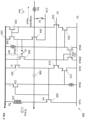
- FIG. 2 is a schematic representation of an integrator circuit 200, in accordance with an embodiment.
- the integrator circuit 200 can be part of an isolated communication bus or the like, for example, a capacitive isolation line at a transmit side of a transformer of a bus.
- the integrator circuit 200 can comprise a first stage driver 202, an integrator input element 204, an inductive load driver 206, and an integrator capacitor 208, which may be the same or similar to those described with reference to FIG. 1 but may be configured and arranged in the circuit 200 in a different manner than the circuit 100 of FIG 1 .
- the first stage driver 202, integrator input element 204, inductive load driver 206, and integrator capacitor 208 can operate to generate an integrator current of 0A in a DC state.
- the circuit 200 can provide an integration of the linear input current at the capacitor 108.
- the inductive load driver 206 operates as a power MOS transistor, which can be biased at 1mA in the DC state.
- the circuit 200 can include a copy MOS transistor 216 having a source coupled to the coil 210 and the capacitor 208, a drain coupled to a current source, for example, a 1mA source, and a gate coupled to the gate of the inductive load driver 206, which in turn has a sufficient current to drive a 30nH coil 210.
- the circuit 200 provides a copy of the inductive load driver current to the copy MOS transistor 216 at which the copy MOS current can be up to 100 times smaller than the inductive load driver current, assuming that the 30mH coil 210 can be a short in the DC state.
- the copy MOS transistor 216 can be set at 10 ⁇ A, or in a range between 5-20 ⁇ A so that the inductive load driver current can be 1 mA, or in a range between 0.5-2mA.
- First and second NMOS transistors 212, 214 can be in series with the first stage driver 202 and drive the gate of the power MOS 206.
- the first NMOS transistor 212 may be set to have a current, e.g., 2mA, at its drain and driven by the first stage driver 202.
- the first stage driver 202 current (e.g., 2mA) can be controlled by a copy of the first stage circuit 202, in particular, a copy NMOS transistor 203, or 10 times smaller.
- the drain current of the copy NMOS transistor 203 can be forced at 200 ⁇ A, or in a range between at 100-300 ⁇ A with a 20 ⁇ A or range between 10-30 ⁇ A current pulldown current source 205 and PMOS mirror transistors 221, 222.
- the drain of the second PMOS mirror transistor 222 can drive the current in the integrator input element 204 through a closed loop transistor 224, wherein a control transistor 226 controls the current at the drain of the closed loop transistor 224 and the mirror transistors 228, 229.
- the integrator current (lint) can be 0A, or a negligible value between 0-1A
- the gate of the integrator input element 204 can be connected to the voltage supply, e.g., 1.5V or a voltage range between 1-5V
- the closed loop controls the current in the integrator input element 204, which in turn can control the first stage driver 202 and the power MOS 206, and permits the power MOS 206 to drive the 30mH coil 110 as a follower stage, for example, driving a 150mA current at the coil 110 in 6ns or less.
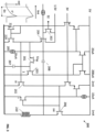
- FIG. 3 is a schematic representation of an electronic integration "integrator" circuit 300, in accordance with another embodiment.
- the integrator circuit 300 can include components constructed and arranged in a similar manner as those of the integrator circuit 200 of FIG. 2 , details of which are not repeated for brevity.
- the integrator circuit 300 can include a first switch 301, e.g., an NMOS transistor and a second switch 302, e.g., an NMOS transistor 302.
- the first switch 301 can be coupled between the copy NMOS transistor 203 and the source of the integrator input element 204.
- the second switch 302 can be coupled between the gate of the integrator input element 204, the voltage source (e.g., 1.5V) and the current source (lint).
- the integrator input element 204 can be attached at a predetermined voltage such as 2.5 V, or 1-3V, with a current range of .5- 2mA, preferably 1mA in the inductive load driver 206, which functions as a final power stage NMOS transistor.
- the switch signals S1, S2 may be applied to the first switch 301 and second switch 302, respectively, to cause the first and second switches to 301, 302 to be in an open state, or inactivated, whereby the first power switch 301 can be turned off by the signal S1 transitioning from 1.5V to 0V to preserve the DC state of the copy NMOS transistor 203 for the pulse duration.
- the capacitor 208 connected between the gate of the copy NMOS transistor 203 and the drain of the first switch transistor 301 can allow the DC state current to be maintained at the integrator input element 204.
- the second switch transistor 302 can be turned off when the signal S2 transitions from a higher voltage, e.g., 3V to a lower voltage, e.g., 1.5V.
- the input switch command (S) begins with the integration current (lint).
- the integrator capacitor 208 e.g., a 1pF capacitor
- the output can have a t 2 shape from 0-2.5V in 6ns, as shown in FIGs. 5 and 6 . According, the S2 signal can drive the t 2 shape.
- the current in the coil 210 reaches a value of around 130 to 150mA with a t 3 shape.
- the integration stops when the S2 signal increases and the linear lint current can be reduced to 0A.
- the signal S2 increases, or changes state, when the coil current can be reduced to 0A, or a negligible current for example, 0-1mA in the DC state.
- the current may return to 0A, or negligible current for example, 0- 1mA at the final power stage 206 in a DC state.
- FIG. 5 and 6 illustrate various voltages and currents across the coil 210.
- the quadratic pulse can be selected over a square pulse and a linear pulse as the preferred command option because it allows the longer pulse of 6ns to provide the same coil current.
- the t 2 shape voltage source across the inductor allows for a longer command to achieve the same maximum current in the coil.
- the current may have a t 3 shape due to the current derivation in t 3 providing a voltage shown in the t 2 shape.
- a perfect integration circuit requires no input current at the integrator input so that the current will flow to an integrator capacitor 408. Also, a perfect integration circuit requires the frequency or the periodic time of the input wave to be less than the circuit time constant. To comply with a desired threshold of 6ns, the integrator operates with few components, i.e., NMOS transistors 402, 404 and no operational amplifier. Components 402, 404, 406, 408, and 410 may be the same as or similar to those components described in the circuits of FIGs 1-3 so details thereof are not repeated for brevity.
- the maximum current at the gate of the inductive load driver transistor 406 ranges from 1-2mA, preferably 1.5mA, which activates the inductive load driver 406.
- the bias current of the first stage driver transistor 402 may be greater than 1.5mA, for example, configured to operate at 2mA.
- the gate current of the inductive load driver 406 may be linear. Accordingly, the drain current of the first stage driver transistor 402 can drop from 2mA to 0.5mA.
- the gate-source voltage (Vgs) of the first stage driver transistor 402 decreases.
- the gate current of the integrator input element 404 e.g., including an NMOS transistor or the like, may be 0A or a negligible current between 0-1mA.
- a significant amount of the bias current of the first stage driver transistor 402 can be applied to the gate of the follower 406. Therefore, the current at the first stage driver transistor 402 may not be constant, resulting in a drop of gate-source voltage (Vg1) of the first stage driver transistor 402.
- a linear current ramp at the source of the NMOS transistor 404 allows the DC bias current to contribute to the maintaining of the integrator input voltage, where little or no current is injected into the integrator input and all the linear input current instead flows into the capacitor 408 to be integrated and achieve the t 2 voltage shape at the opposite side of the capacitor 408.
- gate-source voltage of the NMOS transistor 404 Vg2 increases to compensate for a commensurate decrease in the gate-source voltage of the first stage driver transistor 402 (Vg1).
- the gate current of the NMOS transistor 404 for example, 1nA-100nA. As shown in FIG. 8 , the gate current of the NMOS transistor 404 (A) has an average of about 5nA.
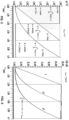
- FIGs. 7 and 8 also illustrate a circuit 400 and its impact of the linear ramp current (B) of the NMOS transistor 404 of 140 ⁇ A in 6ns. Also shown is a plot of the integrator input with (C) and without (D) the linear current of the NMOS transistor 404. To maintain a constant voltage (Vine), the bias current of the integrator input element 404 may increase. As shown in FIG. 8 , the voltage shown at region (inc) can be provided with a constant current 404 (G) and with the current 404 having a current ramp to allow the voltage (Vinc) to be constant. If the gate current at integrator input element 404 is 0, the voltage (Vinc) can be flat (V). Otherwise the voltage decreases, which affects the output voltage.
- Vg1 when the drain current of NMOS transistor 402 changes, the voltage (Vg1) decreases.
- the impact on the output voltage With the linear current of the NMOS transistor 404 at the current source 421, the output voltage may be close to the ideal t2 shape, e.g., reference curve (E). In contrast, curve (F) pertains to an output without the linear current ramp. Here, about 0.7V of the peak amplitude can be lost because a significant amount of the integration current can be applied to the integrator input. With the additional linear current at the NMOS transistor 404, which keeps the integrator input constant, a fast integrator of 6ns pulse can be obtained with the four components (402, 404, 406, and 408) collectively driving 150mA in the 30mH coil 410.
- the four components (402, 404, 406, and 408) collectively driving 150mA in the 30mH coil 410.
- FIG. 9 illustrate an operation that includes generating a linear current ramp from 0-140 ⁇ A in 6ns, for example, how a linear current 521 can be added to an integrator input element 504, e.g., including an NMOS transistor or the like. Reference can also be made to the circuit shown in FIG. 7 .
- a first closed loop DC current 530 goes in the NMOS mirror current transistors 533, 534 with a gain of 2.
- a ramp current may increase from 0-80 ⁇ A in 6ns.
- the active components may be biased, i.e., not in an off state with 0A current. This is illustrated in FIG. 9 .
- the capacitor 538 can be shorted by the integrator input element 532, e.g., including a NMOS transistor or the like so there is no current in the capacitor 538.
- the integrator input element 532 e.g., including a NMOS transistor or the like
- the bias current given by the closed loop can flow in the capacitor 538 and generates the linear B signal from 0 to 550mV.
- the NMOS mirror transistors 537, 539 may be biased with the same current as the current 530, through a closed loop formed by current source 531 and NMOS transistors 533, 534, and 535.
- NMOS transistors are described by way of example, other electromagnetic signal switching electronic devices may equally apply. Therefore, in a DC state, when NMOS transistor 532 coupled to be parallel capacitor 538 is closed, the RC node formed between capacitor 538 and resistor 540 has the same voltage as the voltage (Vgs) of mirror transistor 539 and NMOS mirror current transistor 533, where the resistor 540 has no current.
- the capacitor 538 can be driven by the closed loop formed by current source 531 and NMOS transistors 533, 534, and 535 to receive a constant current equal to currents 530, 531.
- the linear voltage ramp of the capacitor 538 can be applied to the resistance of the resistor 540.
- the NMOS transistor 537 of FIG. 9 can create the current source 421.
- the main currents and voltage of the circuit 500 of FIG. 9 provide a linear current ramp from 0-80 ⁇ A in 6ns (see line IRramp).
- a digital command (A) can drive the linear voltage ramp (VCramp) from 0-550mV in 6ns, or a range of 4ns-8ns but not limited thereto.
- an electronic integration circuit can comprise a first stage driver; an integrator input element coupled between a voltage source, an input current source, and the first stage driver, the integrator input element that provides a final power stage of the electronic integration circuit and provides a constant drain current in a direct current state that controls a current of the first stage driver; an inductive load driver constructed and arranged to drive an inductive element as a voltage follower stage, wherein the inductive load driver processes a linear gate current to control a current output to the inductive element; and a capacitor between the first stage driver and the integrator input element, wherein a sum of a gate-source voltage of the first stage driver and a gate-source voltage of the integrator input element is provided as an integrator input to the capacitor, and wherein the capacitor performs a linear current ramp integration operation to provide a t 2 voltage shape across the inductive element required for driving the inductive element in accordance with the controlled current output in a t 3 shape.
- Alternative embodiments of the electronic integration circuit can include one of the following features, or any combination thereof.
- the integrator input element can provide an additional linear current to maintain a constant integrator input voltage at the integrator input.
- the first stage driver, the integrator input element, the inductive load driver, and the capacitor can collectively produce a 6ns pulse that drives 150mA in the inductive element, and wherein the inductive element can include a 30mH coil.
- the integrator input element can include an NMOS transistor having a source coupled between a current source and a gate of the first stage driver, a drain coupled to the voltage source, and a gate coupled to the input current source.
- At least one of the input current source or a voltage source coupled to the gate of the integrator input element can be constructed and arranged to generate a linear current ramp from 0 to 700 ⁇ A in 6ns.
- the electronic integration circuit can further comprise a voltage switch that places the electronic integration circuit in a direct current state when the integrator input element is connected to a voltage supply by the voltage switch.
- the electronic integration circuit can further comprise a first switching device coupled to a copy NMOS transistor connected to the first stage driver; and a second switching device coupled between the gate of the integrator input element, a voltage source, and a current source, wherein the first and second switching devices are constructed and arranged to maintain a DC state current at the integrator input element for generating an integration of a linear input current in the capacitor.
- the inductive load drive can have a source coupled to both the capacitor and the inductive element.
- the linear current ramp operation can output a linear input current to the capacitor to be integrated and to generate the t 2 voltage shape and injects little or no current at the integrator input element.
- the first stage driver and the integrator input element can provide an integration function so that no input current is in an integrator input signal.
- an electronic integration circuit can comprise an integrator input element coupled to a voltage source and an input current source; a switching device that receives a pulse command that open the switching device to control a current at a gate of the integrator input element and preserve a direct current state of a voltage for a duration of the pulse command; an inductive load driver constructed and arranged to drive an inductive element, wherein the inductive load driver processes a linear gate current to control a current output to the inductive element; and a capacitor at the integrator input element that maintains the DC state at the integrator input element and performs a linear current ramp integration operation according to the pulse command.
- Alternative embodiments of the electronic integration circuit can include one of the following features, or any combination thereof.
- the electronic integration circuit can further comprise a copy NMOS transistor; and another switching device coupled between the copy NMOS transistor and the source of the integrator input element, wherein the other power switch is inactivated by a signal to preserve the DC state of the copy NMOS transistor for the pulse duration.
- the capacitor can be connected between the gate of the copy NMOS transistor and a drain of the other switching device to permit the DC state current to be maintained at the integrator input element.
- the switching device can be turned off when a signal applied to the switching device transitions from a first voltage to a second voltage lower than the first voltage, wherein an input switch command is initiated with an integration current, and as the integration current is received by the capacitor, the electronic integration circuit generates an output having a t 2 shape driven by the signal.
- the t 2 shape can drive the inductive element in accordance with a controlled current output in a t 3 shape.
- the integrator input element can be constructed and arranged to generate a linear current ramp from 0 to 700 ⁇ A.
- a linear current ramp is formed whereby a current of up to 700 ⁇ A flows in the capacitor, an output is generated that drives a current at the inductive element in 6ns or less.
- a driver for a communication bus can comprise an electronic integration circuit, comprising: a first stage driver; an integrator input element coupled between a voltage source, an input current source, and the first stage driver, the integrator input element that provides a final power stage of the electronic integration circuit and provides a constant drain current in a direct current state that controls a current of the first stage driver; an inductive load driver constructed and arranged to drive an inductive element as a voltage follower stage, wherein the inductive load driver processes a linear gate current to control a current output to the inductive element; and a capacitor between the first stage driver and the integrator input element that performs a linear current ramp integration operation for the inductive element.
- the integrator input element can provide an additional linear current to maintain a constant integrator input voltage at the integrator input.
- an output can be generated that drives a current at the inductive element in 6ns or less.
Landscapes
- Physics & Mathematics (AREA)
- Engineering & Computer Science (AREA)
- Mathematical Physics (AREA)
- Theoretical Computer Science (AREA)
- Software Systems (AREA)
- Computer Hardware Design (AREA)
- General Physics & Mathematics (AREA)
- Amplifiers (AREA)
- Electronic Switches (AREA)
Abstract
Description
- The present disclosure relates generally to electronic integration circuits, and more specifically, to an integrator that drives an inductive coil or the like.
- Electronic integration circuits are well-known and readily available for a number of electronic applications. A conventional integrator circuit includes an operational amplifier that provides a desired current response, wave shape, or other signal conditioning functions.
- The presence of an amplifier in an integrator circuit may operate under strict time and peak current conditions, which prohibits the circuit from achieving a combination of ideal characteristics in order to integrate a linear current ramp necessary for driving the integrator input.
- It is desirable that a simple integrator circuit, for example, comprising few transistors including a follower stage, that is capable of driving a high peak current rise, e.g., 130mA, in a coil in 6ns or less.
- The present invention is illustrated by way of example and is not limited by the accompanying figures, in which like references indicate similar elements. Elements in the figures are illustrated for simplicity and clarity and have not necessarily been drawn to scale.
-
FIG. 1 is a block diagram of an integrator circuit, in accordance with some embodiments -
FIG. 2 is a schematic representation of an integrator circuit, in accordance with an embodiment. -
FIG. 3 is a schematic representation of an integrator circuit, in accordance with another embodiment. -
FIG. 4A and 4B are graphs of a voltage and current, respectively, produced by the integrator circuit ofFIG. 3 . -
FIG. 5 is a graph illustrating various pulses produced in the integrator circuit ofFIG. 3 . -
FIG. 6 is a graph of the coil currents corresponding to the pulses illustrated inFIG. 5 . -
FIG. 7 is a schematic representation of an integrator circuit, in accordance with another embodiment. -
FIG. 8 is a graph illustrating various currents formed in the integrator circuit ofFIG. 7 . -
FIG. 9 is a schematic representation of an integrator circuit generating a current source, in accordance with another embodiment. -
FIG. 10 is a graph illustrating various voltages and currents formed in the integrator circuit ofFIG. 9 . - In brief overview, embodiments of the present inventive concept include a simple integrator circuit that can drive a small inductor with an integrator amplifier that generates a quadratic shape pulse based on the integration of a linear ramp current. The integrator circuit operates under strict and tight parameters, in particular, providing a bias current to maintain the integrator input at the same voltage with little or no input current with respect to a small inductor, where the signals having a predetermined longer pulse duration (e.g., 6ns compared to conventional 2ns or 4ns pulse durations) and high peak current (e.g., 150mA). The integrator can be implemented in various electronic applications including, but by no means limited to, automotive, industrial, and consumer applications. One example application may include a 10Mbit/s isolated communication bus for a battery management system (BMS), which requires the integrator to drive a 30nH inductive load requiring a pulse producing a 130mA current in 6ns. Other high speed isolated communication network electronic circuits may equally apply, for example, a microcontroller, battery cell controller, transceiver, and so on.
-
FIG. 1 is a block diagram of anintegrator circuit 100 of acommunication bus 10, in accordance with some embodiments. Theintegrator circuit 100 can be implemented in various electronic applications including, but by no means limited to, automotive, industrial, and consumer applications including signal processing or battery management systems. One application includes the implementation of a computer chip or related electronic integration circuit for a communication bus. - As shown in
FIG. 1 , theintegrator circuit 100 can comprise afirst stage driver 102, anintegrator input element 104, aninductive load driver 106, and anintegrator capacitor 108. In some embodiments, one or more of thefirst stage driver 102, theintegrator input element 104, and theinductive load driver 106 can be formed of Metal-Oxide-Semiconductor Field-Effect Transistors (MOSFETs), and preferably NMOS transistors, but not limited thereto. - The
inductive load driver 106 can be constructed and arranged to drive an inductive load such as acoil 110 as a voltage follower stage. Theinductive load driver 106 can have a source coupled to both theintegrator capacitor 108 and thecoil 110. Thecapacitor 108 can be coupled to the conductive path between theinductive load driver 106 and thecoil 110. Theinductive load driver 106 further has a drain and gate each coupled to acurrent source 122, for example, a 2mA current source. - The
first stage driver 102 can be constructed and arranged to drive the follower stage via the drain of thefirst stage driver 102, which can be in electrical communication with the gate of theinductive load driver 106. In some embodiments, thefirst stage driver 102 can be formed of a source follower circuit, wherein the source of thefirst stage driver 102 can be coupled to ground. The gate of thefirst stage driver 102 can be coupled between a firstcurrent source 121 and a source of theintegrator input element 104. In a DC state, the gate of theintegrator input element 104 can be connected to a voltage supply. In some embodiments, the voltage supply can be a 1.5V voltage supply, for example, provided by aswitching device 103. The voltage may range from 1-2V, but not be limited thereto. Theinput current source 120 coupled to the gate of theintegrator input element 104 can generate a linear current ramp from 0 to 700µA in 6ns. Thefirst stage driver 102 can be biased, for example, at 2mA but not limited thereto, by a closed loop which controls the drain current of theintegrator input 104. - During operation, the
first stage driver 102,integrator input element 104,inductive load driver 106, andintegrator capacitor 108 operate to provide a quadratic output voltage to drive a current in the30nH coil 110 by integrating a linear current ramp in thecapacitor 108. Accordingly, theintegrator circuit 100 requires only three MOS transistors, including the follower stage, to provide a quadratic output voltage of 2.5V in 6ns and drive 120mA in the 30nH coil by integrating a linear current in thecapacitor 108, and produce negligible or no input current (e.g., integrator input element 104) resulting in an integration of the linear input current in theintegrator capacitor 108. -
FIG. 2 is a schematic representation of anintegrator circuit 200, in accordance with an embodiment. As shown, theintegrator circuit 200 can be part of an isolated communication bus or the like, for example, a capacitive isolation line at a transmit side of a transformer of a bus. Theintegrator circuit 200 can comprise afirst stage driver 202, anintegrator input element 204, aninductive load driver 206, and anintegrator capacitor 208, which may be the same or similar to those described with reference toFIG. 1 but may be configured and arranged in thecircuit 200 in a different manner than thecircuit 100 ofFIG 1 . During operation, thefirst stage driver 202,integrator input element 204,inductive load driver 206, andintegrator capacitor 208 can operate to generate an integrator current of 0A in a DC state. To achieve a 1mA bias, thecircuit 200 can provide an integration of the linear input current at thecapacitor 108. - In particular, the
inductive load driver 206 operates as a power MOS transistor, which can be biased at 1mA in the DC state. To achieve the 1mA bias, thecircuit 200 can include acopy MOS transistor 216 having a source coupled to thecoil 210 and thecapacitor 208, a drain coupled to a current source, for example, a 1mA source, and a gate coupled to the gate of theinductive load driver 206, which in turn has a sufficient current to drive a30nH coil 210. Thecircuit 200 provides a copy of the inductive load driver current to thecopy MOS transistor 216 at which the copy MOS current can be up to 100 times smaller than the inductive load driver current, assuming that the30mH coil 210 can be a short in the DC state. For example, as shown inFIG. 2 , thecopy MOS transistor 216 can be set at 10µA, or in a range between 5-20µA so that the inductive load driver current can be 1 mA, or in a range between 0.5-2mA. First andsecond NMOS transistors first stage driver 202 and drive the gate of thepower MOS 206. Thefirst NMOS transistor 212 may be set to have a current, e.g., 2mA, at its drain and driven by thefirst stage driver 202. Thefirst stage driver 202 current (e.g., 2mA) can be controlled by a copy of thefirst stage circuit 202, in particular, acopy NMOS transistor copy NMOS transistor 203 can be forced at 200µA, or in a range between at 100-300µA with a 20µA or range between 10-30µA current pulldowncurrent source 205 andPMOS mirror transistors PMOS mirror transistor 222 can drive the current in theintegrator input element 204 through a closedloop transistor 224, wherein acontrol transistor 226 controls the current at the drain of the closedloop transistor 224 and themirror transistors integrator input element 204 can be connected to the voltage supply, e.g., 1.5V or a voltage range between 1-5V, and the closed loop controls the current in theintegrator input element 204, which in turn can control thefirst stage driver 202 and thepower MOS 206, and permits thepower MOS 206 to drive the30mH coil 110 as a follower stage, for example, driving a 150mA current at thecoil 110 in 6ns or less. -
FIG. 3 is a schematic representation of an electronic integration "integrator"circuit 300, in accordance with another embodiment. Theintegrator circuit 300 can include components constructed and arranged in a similar manner as those of theintegrator circuit 200 ofFIG. 2 , details of which are not repeated for brevity. In addition, theintegrator circuit 300 can include afirst switch 301, e.g., an NMOS transistor and asecond switch 302, e.g., anNMOS transistor 302. Thefirst switch 301 can be coupled between thecopy NMOS transistor 203 and the source of theintegrator input element 204. Thesecond switch 302 can be coupled between the gate of theintegrator input element 204, the voltage source (e.g., 1.5V) and the current source (lint). - During an operation involving voltage driven pulse commands (see
FIGs. 3-6 ), at the pulse starting point (seeFIG. 4 ), theintegrator input element 204 can be attached at a predetermined voltage such as 2.5 V, or 1-3V, with a current range of .5- 2mA, preferably 1mA in theinductive load driver 206, which functions as a final power stage NMOS transistor. When the power command can be initiated, the switch signals S1, S2 may be applied to thefirst switch 301 andsecond switch 302, respectively, to cause the first and second switches to 301, 302 to be in an open state, or inactivated, whereby thefirst power switch 301 can be turned off by the signal S1 transitioning from 1.5V to 0V to preserve the DC state of thecopy NMOS transistor 203 for the pulse duration. Thecapacitor 208 connected between the gate of thecopy NMOS transistor 203 and the drain of thefirst switch transistor 301 can allow the DC state current to be maintained at theintegrator input element 204. - The
second switch transistor 302 can be turned off when the signal S2 transitions from a higher voltage, e.g., 3V to a lower voltage, e.g., 1.5V. The input switch command (S) begins with the integration current (lint). As the totality of the current lint, e.g., up to 700µA, flows in theintegrator capacitor 208, e.g., a 1pF capacitor, the output can have a t2 shape from 0-2.5V in 6ns, as shown inFIGs. 5 and 6 . According, the S2 signal can drive the t2 shape. - At time tend (see
FIGs. 4A, 4B ), when the signal S2 increases, the current in thecoil 210 reaches a value of around 130 to 150mA with a t3 shape. The integration stops when the S2 signal increases and the linear lint current can be reduced to 0A. The signal S2 increases, or changes state, when the coil current can be reduced to 0A, or a negligible current for example, 0-1mA in the DC state. At the end of the coil command, i.e., the rightmost shape shown inFIGs. 5 and 6 , the current may return to 0A, or negligible current for example, 0- 1mA at thefinal power stage 206 in a DC state. -
FIG. 5 and 6 illustrate various voltages and currents across thecoil 210. As shown inFIGs. 5-6 , the quadratic pulse can be selected over a square pulse and a linear pulse as the preferred command option because it allows the longer pulse of 6ns to provide the same coil current. The t2 shape voltage source across the inductor allows for a longer command to achieve the same maximum current in the coil. As U=1dI/dt, the current may have a t3 shape due to the current derivation in t3 providing a voltage shown in the t2 shape. - During an operation involving current integration (see
FIGs. 7-8 ), a perfect integration circuit requires no input current at the integrator input so that the current will flow to anintegrator capacitor 408. Also, a perfect integration circuit requires the frequency or the periodic time of the input wave to be less than the circuit time constant. To comply with a desired threshold of 6ns, the integrator operates with few components, i.e.,NMOS transistors Components FIGs 1-3 so details thereof are not repeated for brevity. - During the linear current ramp integration including the generation of a t2 shape voltage across the
coil 410, the maximum current at the gate of the inductiveload driver transistor 406 ranges from 1-2mA, preferably 1.5mA, which activates theinductive load driver 406. Here, the bias current of the firststage driver transistor 402 may be greater than 1.5mA, for example, configured to operate at 2mA. The gate current of theinductive load driver 406 may be linear. Accordingly, the drain current of the firststage driver transistor 402 can drop from 2mA to 0.5mA. - In doing so, the gate-source voltage (Vgs) of the first stage driver transistor 402 (Vg1) decreases. To achieve an integration, the gate current of the
integrator input element 404, e.g., including an NMOS transistor or the like, may be 0A or a negligible current between 0-1mA. In other words, to achieve a 0uA input current, Vinc = Vg1 + Vg2 of the integrator may be constant during the time integration, for example, Vinc=Vg1+Vg2, where Vg2 is the gate-source voltage of theNMOS transistor 404. However, a significant amount of the bias current of the firststage driver transistor 402 can be applied to the gate of thefollower 406. Therefore, the current at the firststage driver transistor 402 may not be constant, resulting in a drop of gate-source voltage (Vg1) of the firststage driver transistor 402. - The addition of a linear current ramp at the source of the
NMOS transistor 404 allows the DC bias current to contribute to the maintaining of the integrator input voltage, where little or no current is injected into the integrator input and all the linear input current instead flows into thecapacitor 408 to be integrated and achieve the t2 voltage shape at the opposite side of thecapacitor 408. In doing so, gate-source voltage of the NMOS transistor 404 (Vg2) increases to compensate for a commensurate decrease in the gate-source voltage of the first stage driver transistor 402 (Vg1). However, sinceNMOS transistor 404 can be substantially less than that of the firststage driver transistor 402, the gate current of theNMOS transistor 404, for example, 1nA-100nA. As shown inFIG. 8 , the gate current of the NMOS transistor 404 (A) has an average of about 5nA. -
FIGs. 7 and8 also illustrate a circuit 400 and its impact of the linear ramp current (B) of theNMOS transistor 404 of 140µA in 6ns. Also shown is a plot of the integrator input with (C) and without (D) the linear current of theNMOS transistor 404. To maintain a constant voltage (Vine), the bias current of theintegrator input element 404 may increase. As shown inFIG. 8 , the voltage shown at region (inc) can be provided with a constant current 404 (G) and with the current 404 having a current ramp to allow the voltage (Vinc) to be constant. If the gate current atintegrator input element 404 is 0, the voltage (Vinc) can be flat (V). Otherwise the voltage decreases, which affects the output voltage. For example, when the drain current ofNMOS transistor 402 changes, the voltage (Vg1) decreases. In DC state thecurrent source 421 can be adjusted to arrive at Vg1+Vg2 = 1.5V. But when voltage Vg2 goes low, the current 421 may increase to increase voltage Vg2 and maintain Vg1+Vg2 = 1.5V. - Also shown is the impact on the output voltage. With the linear current of the
NMOS transistor 404 at thecurrent source 421, the output voltage may be close to the ideal t2 shape, e.g., reference curve (E). In contrast, curve (F) pertains to an output without the linear current ramp. Here, about 0.7V of the peak amplitude can be lost because a significant amount of the integration current can be applied to the integrator input. With the additional linear current at theNMOS transistor 404, which keeps the integrator input constant, a fast integrator of 6ns pulse can be obtained with the four components (402, 404, 406, and 408) collectively driving 150mA in the30mH coil 410. -
FIG. 9 illustrate an operation that includes generating a linear current ramp from 0-140µA in 6ns, for example, how a linear current 521 can be added to an integrator input element 504, e.g., including an NMOS transistor or the like. Reference can also be made to the circuit shown inFIG. 7 . A first closed loop DC current 530 goes in the NMOS mirrorcurrent transistors FIG. 9 , to accommodate this short timing, the active components may be biased, i.e., not in an off state with 0A current. This is illustrated inFIG. 9 . Thecapacitor 538 can be shorted by theintegrator input element 532, e.g., including a NMOS transistor or the like so there is no current in thecapacitor 538. For example, whenNMOS transistor 532 is open (driven by signal A), the bias current given by the closed loop can flow in thecapacitor 538 and generates the linear B signal from 0 to 550mV. However, theNMOS mirror transistors current source 531 andNMOS transistors - Although NMOS transistors are described by way of example, other electromagnetic signal switching electronic devices may equally apply. Therefore, in a DC state, when
NMOS transistor 532 coupled to beparallel capacitor 538 is closed, the RC node formed betweencapacitor 538 andresistor 540 has the same voltage as the voltage (Vgs) ofmirror transistor 539 and NMOS mirrorcurrent transistor 533, where theresistor 540 has no current. When the signal (A) at the gate of theNMOS transistor 532 is low, thecapacitor 538 can be driven by the closed loop formed bycurrent source 531 andNMOS transistors currents NMOS transistor 535 drives the voltage node (RC), it forces a linear voltage across thecapacitor 538 to generate a constant current equal to I(531)=C dV/dt, where C is the capacitance ofcapacitor 538. Theresistor 540 in parallel with thecapacitor 538 can receive the same linear voltage transformed in a current ramp by the equation I=U/R. The linear voltage ramp of thecapacitor 538 can be applied to the resistance of theresistor 540. As shown inFIG. 7 , theNMOS transistor 537 ofFIG. 9 can create thecurrent source 421. - As shown in
FIG. 10 , the main currents and voltage of thecircuit 500 ofFIG. 9 provide a linear current ramp from 0-80µA in 6ns (see line IRramp). A digital command (A) can drive the linear voltage ramp (VCramp) from 0-550mV in 6ns, or a range of 4ns-8ns but not limited thereto. - As will be appreciated, embodiments as disclosed include at least the following embodiments. In one embodiment, an electronic integration circuit can comprise a first stage driver; an integrator input element coupled between a voltage source, an input current source, and the first stage driver, the integrator input element that provides a final power stage of the electronic integration circuit and provides a constant drain current in a direct current state that controls a current of the first stage driver; an inductive load driver constructed and arranged to drive an inductive element as a voltage follower stage, wherein the inductive load driver processes a linear gate current to control a current output to the inductive element; and a capacitor between the first stage driver and the integrator input element, wherein a sum of a gate-source voltage of the first stage driver and a gate-source voltage of the integrator input element is provided as an integrator input to the capacitor, and wherein the capacitor performs a linear current ramp integration operation to provide a t2 voltage shape across the inductive element required for driving the inductive element in accordance with the controlled current output in a t3 shape.
- Alternative embodiments of the electronic integration circuit can include one of the following features, or any combination thereof.
- The integrator input element can provide an additional linear current to maintain a constant integrator input voltage at the integrator input.
- The first stage driver, the integrator input element, the inductive load driver, and the capacitor can collectively produce a 6ns pulse that drives 150mA in the inductive element, and wherein the inductive element can include a 30mH coil.
- The integrator input element can include an NMOS transistor having a source coupled between a current source and a gate of the first stage driver, a drain coupled to the voltage source, and a gate coupled to the input current source.
- At least one of the input current source or a voltage source coupled to the gate of the integrator input element can be constructed and arranged to generate a linear current ramp from 0 to 700µA in 6ns.
- The electronic integration circuit can further comprise a voltage switch that places the electronic integration circuit in a direct current state when the integrator input element is connected to a voltage supply by the voltage switch.
- The electronic integration circuit can further comprise a first switching device coupled to a copy NMOS transistor connected to the first stage driver; and a second switching device coupled between the gate of the integrator input element, a voltage source, and a current source, wherein the first and second switching devices are constructed and arranged to maintain a DC state current at the integrator input element for generating an integration of a linear input current in the capacitor.
- The inductive load drive can have a source coupled to both the capacitor and the inductive element.
- The linear current ramp operation can output a linear input current to the capacitor to be integrated and to generate the t2 voltage shape and injects little or no current at the integrator input element.
- The first stage driver and the integrator input element can provide an integration function so that no input current is in an integrator input signal.
- In another embodiment, an electronic integration circuit can comprise an integrator input element coupled to a voltage source and an input current source; a switching device that receives a pulse command that open the switching device to control a current at a gate of the integrator input element and preserve a direct current state of a voltage for a duration of the pulse command; an inductive load driver constructed and arranged to drive an inductive element, wherein the inductive load driver processes a linear gate current to control a current output to the inductive element; and a capacitor at the integrator input element that maintains the DC state at the integrator input element and performs a linear current ramp integration operation according to the pulse command.
- Alternative embodiments of the electronic integration circuit can include one of the following features, or any combination thereof.
- The electronic integration circuit can further comprise a copy NMOS transistor; and another switching device coupled between the copy NMOS transistor and the source of the integrator input element, wherein the other power switch is inactivated by a signal to preserve the DC state of the copy NMOS transistor for the pulse duration.
- The capacitor can be connected between the gate of the copy NMOS transistor and a drain of the other switching device to permit the DC state current to be maintained at the integrator input element.
- The switching device can be turned off when a signal applied to the switching device transitions from a first voltage to a second voltage lower than the first voltage, wherein an input switch command is initiated with an integration current, and as the integration current is received by the capacitor, the electronic integration circuit generates an output having a t2 shape driven by the signal.
- The t2 shape can drive the inductive element in accordance with a controlled current output in a t3 shape.
- The integrator input element can be constructed and arranged to generate a linear current ramp from 0 to 700µA. When the linear current ramp is formed whereby a current of up to 700µA flows in the capacitor, an output is generated that drives a current at the inductive element in 6ns or less.
- In another embodiment, a driver for a communication bus can comprise an electronic integration circuit, comprising: a first stage driver; an integrator input element coupled between a voltage source, an input current source, and the first stage driver, the integrator input element that provides a final power stage of the electronic integration circuit and provides a constant drain current in a direct current state that controls a current of the first stage driver; an inductive load driver constructed and arranged to drive an inductive element as a voltage follower stage, wherein the inductive load driver processes a linear gate current to control a current output to the inductive element; and a capacitor between the first stage driver and the integrator input element that performs a linear current ramp integration operation for the inductive element.
- Alternative embodiments of the driver include one of the following features, or any combination thereof.
- The integrator input element can provide an additional linear current to maintain a constant integrator input voltage at the integrator input. When the capacitor forms linear current ramp up to 700µA, an output can be generated that drives a current at the inductive element in 6ns or less.
- Although the invention is described herein with reference to specific embodiments, various modifications and changes can be made without departing from the scope of the present invention as set forth in the claims below. Accordingly, the specification and figures are to be regarded in an illustrative rather than a restrictive sense, and all such modifications are intended to be included within the scope of the present invention. Any benefits, advantages, or solutions to problems that are described herein with regard to specific embodiments are not intended to be construed as a critical, required, or essential feature or element of any or all the claims.
- Unless stated otherwise, terms such as "first" and "second" are used to arbitrarily distinguish between the elements such terms describe. Thus, these terms are not necessarily intended to indicate temporal or other prioritization of such elements.
Claims (13)
- An electronic integration circuit, comprising:a first stage driver;an integrator input element coupled between a voltage source, an input current source, and the first stage driver, the integrator input element that provides a final power stage of the electronic integration circuit and provides a constant drain current in a direct current state that controls a current of the first stage driver;an inductive load driver constructed and arranged to drive an inductive element as a voltage follower stage, wherein the inductive load driver processes a linear gate current to control a current output to the inductive element; anda capacitor between the first stage driver and the integrator input element, wherein a sum of a gate-source voltage of the first stage driver and a gate-source voltage of the integrator input element is provided as an integrator input to the capacitor, and wherein the capacitor performs a linear current ramp integration operation to provide a first exponential voltage shape across the inductive element required for driving the inductive element in accordance with the controlled current output in a second exponential voltage shape.
- The electronic integration circuit of claim 1, wherein the integrator input element provides an additional linear current to maintain a constant integrator input voltage at the integrator input.
- The electronic integration circuit of claim 2, wherein the first stage driver, the integrator input element, the inductive load driver, and the capacitor collectively produce a 6ns pulse that drives 150mA in the inductive element, and wherein the inductive element includes a 30mH coil.
- The electronic integration circuit of any preceding claim, wherein the integrator input element includes an NMOS transistor having a source coupled between a current source and a gate of the first stage driver, a drain coupled to the voltage source, and a gate coupled to the input current source.
- The electronic integration circuit of claim 4, wherein at least one of the input current source or a voltage source coupled to the gate of the integrator input element is constructed and arranged to generate a linear current ramp from 0 to at least 700µA in at most 6ns.
- The electronic integration circuit of claim 4 or 5, further comprising a voltage switch that places the electronic integration circuit in a direct current state when the integrator input element is connected to a voltage supply by the voltage switch.
- The electronic integration circuit of any preceding claim, further comprising:a first switching device coupled to a copy NMOS transistor connected to the first stage driver; anda second switching device coupled between the gate of the integrator input element, the voltage source, and a current source, wherein the first and second switching devices are constructed and arranged to maintain a DC state current at the integrator input element for generating an integration of a linear input current in the capacitor.
- The electronic integration circuit of any preceding claim, wherein the inductive load drive has a source coupled to both the capacitor and the inductive element.
- The electronic integration circuit of any preceding claim, wherein the linear current ramp operation outputs a linear input current to the capacitor to be integrated and to generate the first exponential voltage shape and injects little or no current at the integrator input element.
- The electronic integration circuit of any preceding claim, wherein the first stage driver and the integrator input element provide an integration function so that no input current is in an integrator input signal.
- A driver for a communication bus, comprising:
an electronic integration circuit, comprising:a first stage driver;an integrator input element coupled between a voltage source, an input current source, and the first stage driver, the integrator input element that provides a final power stage of the electronic integration circuit and provides a constant drain current in a direct current state that controls a current of the first stage driver;an inductive load driver constructed and arranged to drive an inductive element as a voltage follower stage, wherein the inductive load driver processes a linear gate current to control a current output to the inductive element; anda capacitor between the first stage driver and the integrator input element that performs a linear current ramp integration operation for the inductive element. - The driver of claim 11, wherein the integrator input element provides an additional linear current to maintain a constant integrator input voltage at the integrator input.
- The driver of claim 11 or 12, wherein when the capacitor forms linear current ramp up to 700µA, an output is generated that drives a current at the inductive element in 6ns or less.
Priority Applications (2)
| Application Number | Priority Date | Filing Date | Title |
|---|---|---|---|
| EP21306564.2A EP4177786B1 (en) | 2021-11-08 | 2021-11-08 | Electronic integrator circuit for driving inductor |
| US17/903,492 US12244314B2 (en) | 2021-11-08 | 2022-09-06 | Electronic integrator circuit for driving inductor |
Applications Claiming Priority (1)
| Application Number | Priority Date | Filing Date | Title |
|---|---|---|---|
| EP21306564.2A EP4177786B1 (en) | 2021-11-08 | 2021-11-08 | Electronic integrator circuit for driving inductor |
Publications (2)
| Publication Number | Publication Date |
|---|---|
| EP4177786A1 true EP4177786A1 (en) | 2023-05-10 |
| EP4177786B1 EP4177786B1 (en) | 2025-01-08 |
Family
ID=78770570
Family Applications (1)
| Application Number | Title | Priority Date | Filing Date |
|---|---|---|---|
| EP21306564.2A Active EP4177786B1 (en) | 2021-11-08 | 2021-11-08 | Electronic integrator circuit for driving inductor |
Country Status (2)
| Country | Link |
|---|---|
| US (1) | US12244314B2 (en) |
| EP (1) | EP4177786B1 (en) |
Citations (1)
| Publication number | Priority date | Publication date | Assignee | Title |
|---|---|---|---|---|
| EP0337857A1 (en) * | 1988-04-14 | 1989-10-18 | Siemens Aktiengesellschaft | Control circuit for an inductive load |
Family Cites Families (3)
| Publication number | Priority date | Publication date | Assignee | Title |
|---|---|---|---|---|
| US6670796B2 (en) | 2002-05-24 | 2003-12-30 | Anritsu Company | Ultra fast and high efficiency inductive coil driver |
| US11362584B2 (en) * | 2019-02-18 | 2022-06-14 | Texas Instruments Incorporated | Adaptive ramp signal generation |
| EP4027528A1 (en) | 2021-01-08 | 2022-07-13 | NXP USA, Inc. | Communications system |
-
2021
- 2021-11-08 EP EP21306564.2A patent/EP4177786B1/en active Active
-
2022
- 2022-09-06 US US17/903,492 patent/US12244314B2/en active Active
Patent Citations (1)
| Publication number | Priority date | Publication date | Assignee | Title |
|---|---|---|---|---|
| EP0337857A1 (en) * | 1988-04-14 | 1989-10-18 | Siemens Aktiengesellschaft | Control circuit for an inductive load |
Non-Patent Citations (1)
| Title |
|---|
| GROENEWOLD G ET AL: "SYSTEMATIC DISTORTION ANALYSIS FOR MOSFET INTEGRATORS WITH USE OF ANEW MOSFET MODEL", IEEE TRANSACTIONS ON CIRCUITS AND SYSTEMS II: ANALOG AND DIGITAL SIGNAL PROCESSING, INSTITUTE OF ELECTRICAL AND ELECTRONICS ENGINEERS INC, 345 EAST 47 STREET , NEW YORK N Y 10017 , USA, vol. 41, no. 9, 1 September 1994 (1994-09-01), pages 569 - 580, XP000468158, ISSN: 1057-7130, DOI: 10.1109/82.326583 * |
Also Published As
| Publication number | Publication date |
|---|---|
| US20230147110A1 (en) | 2023-05-11 |
| EP4177786B1 (en) | 2025-01-08 |
| US12244314B2 (en) | 2025-03-04 |
Similar Documents
| Publication | Publication Date | Title |
|---|---|---|
| US8120338B2 (en) | Dropper-type regulator | |
| US10243467B2 (en) | Voltage regulators with kickback protection | |
| US5796276A (en) | High-side-driver gate drive circuit | |
| US10295577B1 (en) | Current sensor with extended voltage range | |
| CN108255228B (en) | Circuit for reducing negative pulse signal at output end in voltage stabilizer and method of voltage stabilization | |
| KR102665144B1 (en) | Circuits and methods for slew rate control of switched capacitor regulators | |
| EP1274067B1 (en) | Driver Circuit | |
| JP7728684B2 (en) | Switching circuit, DC/DC converter and its control circuit | |
| US4877982A (en) | MOSFET turn-on/off circuit | |
| JP7378372B2 (en) | semiconductor equipment | |
| EP3923683A1 (en) | Led array driver system | |
| WO2020047119A1 (en) | Gan driver using active pre-driver with feedback | |
| US20240053781A1 (en) | Low-dropout regulator with inrush current limiting capabilities | |
| US10230356B2 (en) | High-side output transistor circuit | |
| US20230268918A1 (en) | Switching device | |
| EP4177786B1 (en) | Electronic integrator circuit for driving inductor | |
| US10819236B2 (en) | Control of a power stage of a switched-mode power supply | |
| US8471601B2 (en) | Single-ended to differential converter | |
| US20180062641A1 (en) | Drive method and drive circuit for power switch, and power supply system | |
| US20090134922A1 (en) | Start-up circuit for bias circuit | |
| US12549102B2 (en) | Low-power continuous-rail switching regulator architecture | |
| US6130569A (en) | Method and apparatus for a controlled transition rate driver | |
| CN106921373B (en) | Drive circuit | |
| CN105191135B (en) | Gate driving circuit | |
| USRE41728E1 (en) | High linearity, low power voltage controlled resistor |
Legal Events
| Date | Code | Title | Description |
|---|---|---|---|
| PUAI | Public reference made under article 153(3) epc to a published international application that has entered the european phase |
Free format text: ORIGINAL CODE: 0009012 |
|
| STAA | Information on the status of an ep patent application or granted ep patent |
Free format text: STATUS: THE APPLICATION HAS BEEN PUBLISHED |
|
| AK | Designated contracting states |
Kind code of ref document: A1 Designated state(s): AL AT BE BG CH CY CZ DE DK EE ES FI FR GB GR HR HU IE IS IT LI LT LU LV MC MK MT NL NO PL PT RO RS SE SI SK SM TR |
|
| STAA | Information on the status of an ep patent application or granted ep patent |
Free format text: STATUS: REQUEST FOR EXAMINATION WAS MADE |
|
| 17P | Request for examination filed |
Effective date: 20231110 |
|
| RBV | Designated contracting states (corrected) |
Designated state(s): AL AT BE BG CH CY CZ DE DK EE ES FI FR GB GR HR HU IE IS IT LI LT LU LV MC MK MT NL NO PL PT RO RS SE SI SK SM TR |
|
| STAA | Information on the status of an ep patent application or granted ep patent |
Free format text: STATUS: EXAMINATION IS IN PROGRESS |
|
| 17Q | First examination report despatched |
Effective date: 20240415 |
|
| GRAP | Despatch of communication of intention to grant a patent |
Free format text: ORIGINAL CODE: EPIDOSNIGR1 |
|
| STAA | Information on the status of an ep patent application or granted ep patent |
Free format text: STATUS: GRANT OF PATENT IS INTENDED |
|
| INTG | Intention to grant announced |
Effective date: 20240904 |
|
| GRAS | Grant fee paid |
Free format text: ORIGINAL CODE: EPIDOSNIGR3 |
|
| GRAA | (expected) grant |
Free format text: ORIGINAL CODE: 0009210 |
|
| STAA | Information on the status of an ep patent application or granted ep patent |
Free format text: STATUS: THE PATENT HAS BEEN GRANTED |
|
| AK | Designated contracting states |
Kind code of ref document: B1 Designated state(s): AL AT BE BG CH CY CZ DE DK EE ES FI FR GB GR HR HU IE IS IT LI LT LU LV MC MK MT NL NO PL PT RO RS SE SI SK SM TR |
|
| REG | Reference to a national code |
Ref country code: GB Ref legal event code: FG4D |
|
| REG | Reference to a national code |
Ref country code: CH Ref legal event code: EP |
|
| REG | Reference to a national code |
Ref country code: DE Ref legal event code: R096 Ref document number: 602021024627 Country of ref document: DE |
|
| REG | Reference to a national code |
Ref country code: IE Ref legal event code: FG4D |
|
| REG | Reference to a national code |
Ref country code: LT Ref legal event code: MG9D |
|
| REG | Reference to a national code |
Ref country code: NL Ref legal event code: MP Effective date: 20250108 |
|
| REG | Reference to a national code |
Ref country code: AT Ref legal event code: MK05 Ref document number: 1758814 Country of ref document: AT Kind code of ref document: T Effective date: 20250108 |
|
| PG25 | Lapsed in a contracting state [announced via postgrant information from national office to epo] |
Ref country code: NL Free format text: LAPSE BECAUSE OF FAILURE TO SUBMIT A TRANSLATION OF THE DESCRIPTION OR TO PAY THE FEE WITHIN THE PRESCRIBED TIME-LIMIT Effective date: 20250108 |
|
| PG25 | Lapsed in a contracting state [announced via postgrant information from national office to epo] |
Ref country code: RS Free format text: LAPSE BECAUSE OF FAILURE TO SUBMIT A TRANSLATION OF THE DESCRIPTION OR TO PAY THE FEE WITHIN THE PRESCRIBED TIME-LIMIT Effective date: 20250408 |
|
| PG25 | Lapsed in a contracting state [announced via postgrant information from national office to epo] |
Ref country code: FI Free format text: LAPSE BECAUSE OF FAILURE TO SUBMIT A TRANSLATION OF THE DESCRIPTION OR TO PAY THE FEE WITHIN THE PRESCRIBED TIME-LIMIT Effective date: 20250108 |
|
| PG25 | Lapsed in a contracting state [announced via postgrant information from national office to epo] |
Ref country code: PL Free format text: LAPSE BECAUSE OF FAILURE TO SUBMIT A TRANSLATION OF THE DESCRIPTION OR TO PAY THE FEE WITHIN THE PRESCRIBED TIME-LIMIT Effective date: 20250108 |
|
| PG25 | Lapsed in a contracting state [announced via postgrant information from national office to epo] |
Ref country code: ES Free format text: LAPSE BECAUSE OF FAILURE TO SUBMIT A TRANSLATION OF THE DESCRIPTION OR TO PAY THE FEE WITHIN THE PRESCRIBED TIME-LIMIT Effective date: 20250108 |
|
| PG25 | Lapsed in a contracting state [announced via postgrant information from national office to epo] |
Ref country code: IS Free format text: LAPSE BECAUSE OF FAILURE TO SUBMIT A TRANSLATION OF THE DESCRIPTION OR TO PAY THE FEE WITHIN THE PRESCRIBED TIME-LIMIT Effective date: 20250508 Ref country code: NO Free format text: LAPSE BECAUSE OF FAILURE TO SUBMIT A TRANSLATION OF THE DESCRIPTION OR TO PAY THE FEE WITHIN THE PRESCRIBED TIME-LIMIT Effective date: 20250408 |
|
| PG25 | Lapsed in a contracting state [announced via postgrant information from national office to epo] |
Ref country code: HR Free format text: LAPSE BECAUSE OF FAILURE TO SUBMIT A TRANSLATION OF THE DESCRIPTION OR TO PAY THE FEE WITHIN THE PRESCRIBED TIME-LIMIT Effective date: 20250108 |
|
| PG25 | Lapsed in a contracting state [announced via postgrant information from national office to epo] |
Ref country code: LV Free format text: LAPSE BECAUSE OF FAILURE TO SUBMIT A TRANSLATION OF THE DESCRIPTION OR TO PAY THE FEE WITHIN THE PRESCRIBED TIME-LIMIT Effective date: 20250108 Ref country code: PT Free format text: LAPSE BECAUSE OF FAILURE TO SUBMIT A TRANSLATION OF THE DESCRIPTION OR TO PAY THE FEE WITHIN THE PRESCRIBED TIME-LIMIT Effective date: 20250508 |
|
| PG25 | Lapsed in a contracting state [announced via postgrant information from national office to epo] |
Ref country code: GR Free format text: LAPSE BECAUSE OF FAILURE TO SUBMIT A TRANSLATION OF THE DESCRIPTION OR TO PAY THE FEE WITHIN THE PRESCRIBED TIME-LIMIT Effective date: 20250409 Ref country code: BG Free format text: LAPSE BECAUSE OF FAILURE TO SUBMIT A TRANSLATION OF THE DESCRIPTION OR TO PAY THE FEE WITHIN THE PRESCRIBED TIME-LIMIT Effective date: 20250108 |
|
| PG25 | Lapsed in a contracting state [announced via postgrant information from national office to epo] |
Ref country code: AT Free format text: LAPSE BECAUSE OF FAILURE TO SUBMIT A TRANSLATION OF THE DESCRIPTION OR TO PAY THE FEE WITHIN THE PRESCRIBED TIME-LIMIT Effective date: 20250108 |
|
| PG25 | Lapsed in a contracting state [announced via postgrant information from national office to epo] |
Ref country code: SE Free format text: LAPSE BECAUSE OF FAILURE TO SUBMIT A TRANSLATION OF THE DESCRIPTION OR TO PAY THE FEE WITHIN THE PRESCRIBED TIME-LIMIT Effective date: 20250108 |
|
| PG25 | Lapsed in a contracting state [announced via postgrant information from national office to epo] |
Ref country code: SM Free format text: LAPSE BECAUSE OF FAILURE TO SUBMIT A TRANSLATION OF THE DESCRIPTION OR TO PAY THE FEE WITHIN THE PRESCRIBED TIME-LIMIT Effective date: 20250108 |
|
| REG | Reference to a national code |
Ref country code: DE Ref legal event code: R097 Ref document number: 602021024627 Country of ref document: DE |
|
| PG25 | Lapsed in a contracting state [announced via postgrant information from national office to epo] |
Ref country code: DK Free format text: LAPSE BECAUSE OF FAILURE TO SUBMIT A TRANSLATION OF THE DESCRIPTION OR TO PAY THE FEE WITHIN THE PRESCRIBED TIME-LIMIT Effective date: 20250108 |
|
| PG25 | Lapsed in a contracting state [announced via postgrant information from national office to epo] |
Ref country code: EE Free format text: LAPSE BECAUSE OF FAILURE TO SUBMIT A TRANSLATION OF THE DESCRIPTION OR TO PAY THE FEE WITHIN THE PRESCRIBED TIME-LIMIT Effective date: 20250108 Ref country code: CZ Free format text: LAPSE BECAUSE OF FAILURE TO SUBMIT A TRANSLATION OF THE DESCRIPTION OR TO PAY THE FEE WITHIN THE PRESCRIBED TIME-LIMIT Effective date: 20250108 |
|
| PG25 | Lapsed in a contracting state [announced via postgrant information from national office to epo] |
Ref country code: RO Free format text: LAPSE BECAUSE OF FAILURE TO SUBMIT A TRANSLATION OF THE DESCRIPTION OR TO PAY THE FEE WITHIN THE PRESCRIBED TIME-LIMIT Effective date: 20250108 |
|
| PG25 | Lapsed in a contracting state [announced via postgrant information from national office to epo] |
Ref country code: SK Free format text: LAPSE BECAUSE OF FAILURE TO SUBMIT A TRANSLATION OF THE DESCRIPTION OR TO PAY THE FEE WITHIN THE PRESCRIBED TIME-LIMIT Effective date: 20250108 |
|
| PLBE | No opposition filed within time limit |
Free format text: ORIGINAL CODE: 0009261 |
|
| STAA | Information on the status of an ep patent application or granted ep patent |
Free format text: STATUS: NO OPPOSITION FILED WITHIN TIME LIMIT |
|
| 26N | No opposition filed |
Effective date: 20251009 |
|
| PGFP | Annual fee paid to national office [announced via postgrant information from national office to epo] |
Ref country code: DE Payment date: 20251022 Year of fee payment: 5 |
|
| PGFP | Annual fee paid to national office [announced via postgrant information from national office to epo] |
Ref country code: GB Payment date: 20251023 Year of fee payment: 5 |
|
| PG25 | Lapsed in a contracting state [announced via postgrant information from national office to epo] |
Ref country code: IT Free format text: LAPSE BECAUSE OF FAILURE TO SUBMIT A TRANSLATION OF THE DESCRIPTION OR TO PAY THE FEE WITHIN THE PRESCRIBED TIME-LIMIT Effective date: 20250108 |