EP4175170A1 - Surface acoustic wave (saw) structures with transverse mode suppression - Google Patents

Surface acoustic wave (saw) structures with transverse mode suppression Download PDF

Info

Publication number
EP4175170A1
EP4175170A1 EP22202612.2A EP22202612A EP4175170A1 EP 4175170 A1 EP4175170 A1 EP 4175170A1 EP 22202612 A EP22202612 A EP 22202612A EP 4175170 A1 EP4175170 A1 EP 4175170A1
Authority
EP
European Patent Office
Prior art keywords
saw filter
finger
saw
width
terminal end
Prior art date
Legal status (The legal status is an assumption and is not a legal conclusion. Google has not performed a legal analysis and makes no representation as to the accuracy of the status listed.)
Pending
Application number
EP22202612.2A
Other languages
German (de)
French (fr)
Inventor
Tsuyoshi Yokoyama
Tabito Tanaka
Jun Sung Chun
Current Assignee (The listed assignees may be inaccurate. Google has not performed a legal analysis and makes no representation or warranty as to the accuracy of the list.)
Qorvo US Inc
Original Assignee
Qorvo US Inc
Priority date (The priority date is an assumption and is not a legal conclusion. Google has not performed a legal analysis and makes no representation as to the accuracy of the date listed.)
Filing date
Publication date
Application filed by Qorvo US Inc filed Critical Qorvo US Inc
Publication of EP4175170A1 publication Critical patent/EP4175170A1/en
Pending legal-status Critical Current

Links

Images

Classifications

    • HELECTRICITY
    • H03ELECTRONIC CIRCUITRY
    • H03HIMPEDANCE NETWORKS, e.g. RESONANT CIRCUITS; RESONATORS
    • H03H9/00Networks comprising electromechanical or electro-acoustic elements; Electromechanical resonators
    • H03H9/02Details
    • H03H9/02535Details of surface acoustic wave devices
    • H03H9/02637Details concerning reflective or coupling arrays
    • H03H9/02685Grating lines having particular arrangements
    • H03H9/02724Comb like grating lines
    • H03H9/02732Bilateral comb like grating lines
    • HELECTRICITY
    • H03ELECTRONIC CIRCUITRY
    • H03HIMPEDANCE NETWORKS, e.g. RESONANT CIRCUITS; RESONATORS
    • H03H9/00Networks comprising electromechanical or electro-acoustic elements; Electromechanical resonators
    • H03H9/02Details
    • H03H9/02535Details of surface acoustic wave devices
    • H03H9/02818Means for compensation or elimination of undesirable effects
    • H03H9/02858Means for compensation or elimination of undesirable effects of wave front distortion
    • HELECTRICITY
    • H03ELECTRONIC CIRCUITRY
    • H03HIMPEDANCE NETWORKS, e.g. RESONANT CIRCUITS; RESONATORS
    • H03H9/00Networks comprising electromechanical or electro-acoustic elements; Electromechanical resonators
    • H03H9/02Details
    • H03H9/02007Details of bulk acoustic wave devices
    • H03H9/02015Characteristics of piezoelectric layers, e.g. cutting angles
    • HELECTRICITY
    • H03ELECTRONIC CIRCUITRY
    • H03HIMPEDANCE NETWORKS, e.g. RESONANT CIRCUITS; RESONATORS
    • H03H9/00Networks comprising electromechanical or electro-acoustic elements; Electromechanical resonators
    • H03H9/02Details
    • H03H9/02535Details of surface acoustic wave devices
    • H03H9/02818Means for compensation or elimination of undesirable effects
    • H03H9/02881Means for compensation or elimination of undesirable effects of diffraction of wave beam
    • HELECTRICITY
    • H03ELECTRONIC CIRCUITRY
    • H03HIMPEDANCE NETWORKS, e.g. RESONANT CIRCUITS; RESONATORS
    • H03H9/00Networks comprising electromechanical or electro-acoustic elements; Electromechanical resonators
    • H03H9/02Details
    • H03H9/125Driving means, e.g. electrodes, coils
    • H03H9/145Driving means, e.g. electrodes, coils for networks using surface acoustic waves
    • H03H9/14517Means for weighting
    • H03H9/1452Means for weighting by finger overlap length, apodisation
    • HELECTRICITY
    • H03ELECTRONIC CIRCUITRY
    • H03HIMPEDANCE NETWORKS, e.g. RESONANT CIRCUITS; RESONATORS
    • H03H9/00Networks comprising electromechanical or electro-acoustic elements; Electromechanical resonators
    • H03H9/02Details
    • H03H9/125Driving means, e.g. electrodes, coils
    • H03H9/145Driving means, e.g. electrodes, coils for networks using surface acoustic waves
    • H03H9/14517Means for weighting
    • H03H9/14529Distributed tap
    • H03H9/14532Series weighting; Transverse weighting
    • HELECTRICITY
    • H03ELECTRONIC CIRCUITRY
    • H03HIMPEDANCE NETWORKS, e.g. RESONANT CIRCUITS; RESONATORS
    • H03H9/00Networks comprising electromechanical or electro-acoustic elements; Electromechanical resonators
    • H03H9/02Details
    • H03H9/125Driving means, e.g. electrodes, coils
    • H03H9/145Driving means, e.g. electrodes, coils for networks using surface acoustic waves
    • H03H9/14544Transducers of particular shape or position
    • H03H9/1457Transducers having different finger widths
    • HELECTRICITY
    • H03ELECTRONIC CIRCUITRY
    • H03HIMPEDANCE NETWORKS, e.g. RESONANT CIRCUITS; RESONATORS
    • H03H9/00Networks comprising electromechanical or electro-acoustic elements; Electromechanical resonators
    • H03H9/46Filters
    • H03H9/54Filters comprising resonators of piezoelectric or electrostrictive material
    • HELECTRICITY
    • H03ELECTRONIC CIRCUITRY
    • H03HIMPEDANCE NETWORKS, e.g. RESONANT CIRCUITS; RESONATORS
    • H03H9/00Networks comprising electromechanical or electro-acoustic elements; Electromechanical resonators
    • H03H9/46Filters
    • H03H9/64Filters using surface acoustic waves
    • HELECTRICITY
    • H03ELECTRONIC CIRCUITRY
    • H03HIMPEDANCE NETWORKS, e.g. RESONANT CIRCUITS; RESONATORS
    • H03H9/00Networks comprising electromechanical or electro-acoustic elements; Electromechanical resonators
    • H03H9/46Filters
    • H03H9/64Filters using surface acoustic waves
    • H03H9/6423Means for obtaining a particular transfer characteristic
    • H03H9/6433Coupled resonator filters
    • H03H9/644Coupled resonator filters having two acoustic tracks
    • H03H9/6443Coupled resonator filters having two acoustic tracks being acoustically coupled
    • H03H9/6453Coupled resonator filters having two acoustic tracks being acoustically coupled by at least an interdigital transducer overlapping both tracks
    • HELECTRICITY
    • H03ELECTRONIC CIRCUITRY
    • H03HIMPEDANCE NETWORKS, e.g. RESONANT CIRCUITS; RESONATORS
    • H03H9/00Networks comprising electromechanical or electro-acoustic elements; Electromechanical resonators
    • H03H9/02Details
    • H03H9/02007Details of bulk acoustic wave devices
    • H03H9/02157Dimensional parameters, e.g. ratio between two dimension parameters, length, width or thickness

Definitions

  • SAW surface acoustic wave
  • exemplary aspects of the present disclosure provide digits or fingers with broad interior terminal end shapes. By providing such shapes, spurious modes above the resonance frequency of the SAW structure are suppressed thereby providing desired out-of-band rejection that helps satisfy design criteria such as keeping a higher quality factor (Q) value, a higher electromechanical coupling factor (K2) value, and better Temperature Coefficient of Frequency (TCF).
  • Q quality factor
  • K2 electromechanical coupling factor
  • TCF Temperature Coefficient of Frequency
  • FIGs 1A and 1B illustrate a conventional guided SAW structure 100 having a support substrate 102 on which a piezoelectric layer 104 is positioned.
  • Interdigitated electrodes 106, 108 are positioned on the piezoelectric layer 104 as better seen in Figure 1B .
  • the interdigitated electrodes 106, 108 form an interdigital transducer (IDT) 110 with optional reflectors 112, 114.
  • IDT interdigital transducer
  • one of the interdigitated electrodes 106, 108 may be a dummy electrode.

Landscapes

  • Physics & Mathematics (AREA)
  • Acoustics & Sound (AREA)
  • Surface Acoustic Wave Elements And Circuit Networks Thereof (AREA)

Abstract

Surface acoustic wave, SAW, structures with transverse mode suppression are disclosed. In one aspect, the SAW structure provides digits or fingers (306(1)-306(N), 314(1)-314(N)) with broad interior terminal end shapes (312(1), 312(X), 318(1), 318(X)). By providing such shapes spurious modes above the resonance frequency of the SAW are suppressed thereby providing desired out of band rejection that helps satisfy design criteria such as keeping a higher Q value, a higher K2 value and better Temperature Coefficient of Frequency, TCF.

Description

    BACKGROUND I. Field
  • The technology of the disclosure relates generally to surface acoustic waves and ways to reduce transverse modes spurious around resonance frequencies.
  • II. Background
  • Surface acoustic wave (SAW) devices, such as SAW resonators and SAW filters, are used in many applications such as radio frequency (RF) filters. For example, SAW filters are commonly used in Second Generation (2G), Third Generation (3G), and Fourth Generation (4G) wireless transceiver front ends, duplexers, and receive filters. The widespread use of SAW filters is due to, at least in part, that fact that SAW filters exhibit low insertion loss with good rejection, can achieve broad bandwidths, and are a small fraction of the size of traditional cavity and ceramic filters. As with any electronic device, the performance of a SAW device is an important parameter that can impact the overall performance of a system. In this regard, there is a need for a high-performance SAW device. One such solution is a guided SAW device.
  • Guided SAW devices (i.e., SAW devices having a guided SAW structure) have a layered substrate where a layer of piezoelectric material, which is referred to here as a piezoelectric layer, is bonded or deposited on (e.g., directly on) the surface of a support, or carrier, substrate. As compared to conventional SAW devices, guided SAW devices have an improved quality factor (Q), an improved electromechanical coupling factor (K2), and an improved Temperature Coefficient of Frequency (TCF). However, unwanted spurious modes are typically generated in a guided SAW structure, which hinders a practical use of a guided SAW device. In particular, in a guided SAW device, spurious modes are generated above the resonance frequency of the guided SAW device and, as a result, out-of-band rejection specifications may not be satisfied. Accordingly, there is still a need for improved performance from SAW devices.
  • SUMMARY
  • Particular aspects are set out in the appended independent claims. Various optional embodiments are set out in the dependent claims.
  • Aspects disclosed in the detailed description include surface acoustic wave (SAW) structures with transverse mode suppression. In particular, exemplary aspects of the present disclosure provide digits or fingers with broad interior terminal end shapes. By providing such shapes, spurious modes above the resonance frequency of the SAW structure are suppressed thereby providing desired out-of-band rejection that helps satisfy design criteria such as keeping a higher quality factor (Q) value, a higher electromechanical coupling factor (K2) value, and better Temperature coefficient of Frequency (TCF).
  • In this regard in one aspect, a SAW filter is disclosed. The SAW filter comprises a first interdigitated electrode comprising a first finger. The first finger has a first width along a longitudinal axis of the first finger for a first length and a second width along the longitudinal axis of the first finger for a second length at a terminal end portion of the first finger. The SAW filter also comprises a second interdigitated electrode.
  • BRIEF DESCRIPTION OF THE DRAWINGS
    • Figure 1A is a side elevational view of a guided surface acoustic wave (SAW) structure;
    • Figure 1B is a top plan view of the guided SAW structure of Figure 1B with apodization of the interdigital structure;
    • Figure 2 provides performance graphs for the guided SAW structure of Figures 1A and 1B with transverse modes above the resonant frequency highlighted;
    • Figure 3A illustrates a guided SAW structure with transverse mode suppression according to an exemplary aspect of the present disclosure;
    • Figure 3B illustrates an exemplary finger end used on the interdigital structure to facilitate transverse mode suppression;
    • Figures 4 provides performance graphs for the guided SAW structure with wide finger ends of Figures 3A and 3B highlighting the suppressed transverse modes;
    • Figures 5A and 5B illustrate how changing a width of a finger end relative to the finger shaft affects a magnitude of a transverse mode;
    • Figure 5C illustrates how changing the area of a finger end affects a magnitude of a transverse mode;
    • Figures 6A and 6B illustrate how changing a gap between finger ends affects a magnitude of a transverse mode;
    • Figures 7A and 7B illustrate how changing a crossing gap between fingers affects a magnitude of a transverse mode;
    • Figure 8 illustrates various alternate finger ends;
    • Figures 9A and 9B illustrate how changing a substrate thickness may affect a magnitude of a transverse mode; and
    • Figure 10 illustrates a top plan view of an alternate guided SAW structure with a chirped wave apodization.
    DETAILED DESCRIPTION
  • With reference now to the drawing figures, several exemplary aspects of the present disclosure are described. The word "exemplary" is used herein to mean "serving as an example, instance, or illustration." Any aspect described herein as "exemplary" is not necessarily to be construed as preferred or advantageous over other aspects.
  • Aspects disclosed in the detailed description include surface acoustic wave (SAW) structures with transverse mode suppression. In particular, exemplary aspects of the present disclosure provide digits or fingers with broad interior terminal end shapes. By providing such shapes, spurious modes above the resonance frequency of the SAW structure are suppressed thereby providing desired out-of-band rejection that helps satisfy design criteria such as keeping a higher quality factor (Q) value, a higher electromechanical coupling factor (K2) value, and better Temperature Coefficient of Frequency (TCF).
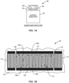
  • Figures 1A and 1B illustrate a conventional guided SAW structure 100 having a support substrate 102 on which a piezoelectric layer 104 is positioned. Interdigitated electrodes 106, 108 are positioned on the piezoelectric layer 104 as better seen in Figure 1B. The interdigitated electrodes 106, 108 form an interdigital transducer (IDT) 110 with optional reflectors 112, 114. Further, one of the interdigitated electrodes 106, 108 (e.g., electrode 108) may be a dummy electrode.
  • With continued reference to Figure 1B, each interdigitated electrode 106, 108 includes a respective plurality of fingers 106A, 108A that are aligned with one another and are separated by gaps 116. The alignment and presence of the gaps 116 provide apodization of the IDT 110.
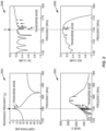
  • Figure 2 provides various graphs 200A-200D showing performance of the guided SAW structure 100 against frequency, and particularly shows a resonance frequency fs with transverse modes proximate the resonance frequency highlighted. As is readily apparent, while the apodization does some work at suppressing the transverse modes, it is insufficient for some purposes.
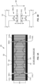
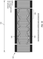
  • As illustrated in Figures 3A and 3B, exemplary aspects of the present disclosure provide a guided SAW filter 300 that includes a first interdigitated electrode 302 and a second interdigitated electrode 304 that are apodized. The first interdigitated electrode 302 has a plurality of fingers 306(1)-306(N) with an exemplary finger 306(X) shown in Figure 3B. Each of the fingers 306(1)-306(N) has a first width W1 along a longitudinal axis 308 of the fingers 306(1)-306(N). The first width W1 is provided along this longitudinal axis 308 for a first length defined by the distance between a lateral bar 310 and a terminal end portion 312(1)-312(N) of the finger 306(1)-306(N). The terminal end portion 312(1)-312(N) of the finger 306(1)-306(N) has a second width W2 along the longitudinal axis 308 for a second length L (see also Figure 5A). The apodization is perpendicular to the longitudinal axis 308 and may be described as being along a length direction of the SAW structure 100. Further, the apodization is formed in a wave pattern and may follow a sine or cosine wave pattern.
  • Similarly, the second interdigitated electrode 304 has a plurality of fingers 314(1)-314(N) with an exemplary finger 314(X) shown in Figure 3B. Each of the fingers 314(1)-314(N) has a first width W1 along the longitudinal axis 308. The first width W1 is provided along this longitudinal axis 308 for a length defined by the distance between a lateral bar 316 and a terminal end portion 318(1)-318(N) of the finger 314(1)-314(N). The terminal end portion 318(1)-318(N) of the finger 314(1)-314(N) has a second width W2 along the longitudinal axis 308 for a second length L (see also Figure 5A).
  • Note that as illustrated, both the fingers 306(1)-306(N) and the fingers 314(1)-314(N) include the wider terminal end portions 312(1)-312(N), 318(1)-318(N). However, the disclosure is not so limited and only one or the other of the fingers 306(1)-306(N) or 314(1)-314(N) may include the wider terminal end portions 312(1)-312(N), 318(1)-318(N). Note further, that as illustrated, the widths W1 of the fingers 306(1)-306(N) are the same as the widths W1 of the fingers 314(1)-314(N), but such identity is not required by the present disclosure and the W1 of fingers 306(1)-306(N) may differ from the W1 of the fingers 314(1)-314(N). Still further, even if both fingers 306(1)-306(N) and 314(1)-314(N) have the wider terminal end portions 312(1)-312(N), 318(1)-318(N), they do not necessarily have to have the same widths W2 relative to each other.
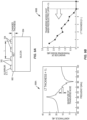
  • Figure 4 provides graphs 400A-400C illustrating how the guided SAW filter 300 suppresses the transverse modes. For reference, the wave amplitude of the apodization is 2.4λ. The aperture 320, length 322, and IDT length/wave were set to 20λ, 100λ, and 10λ, respectively. By using the wide finger ends, the transverse modes can be significantly suppressed, and Q also improves. λ is an interdigital transducer (IDT) period of the SAW filter 300.
  • There are a number of parameters associated with the finger ends which may be optimized to achieve desired transverse mode suppression. Figure 5A is provided which merely reillustrates an exemplary finger 306(X). Figures 5B and 5C illustrate the ramifications of two parameter variations. Figure 5B illustrates how changing the ratio of W2/W1 will affect how much the transverse mode is suppressed while Figure 5C illustrates how changing L and the area of the terminal end portion 312(X) will affect how much the transverse mode is suppressed
  • In this regard, Figure 5B shows graphs 500A and 500B with L set to 0,1λ and various W2/W1 ratios. Specifically, ratios of 1.2, 1.8, and 2.2 are illustrated, with the transverse mode being increasing suppressed as the W2/W1 ratio increases. However, if the W2/W1 ratio is too large (i.e., W2 is too wide), there may be bridging to an adjacent finger, so the W2/W1 ratio may have a practical limit of three (3) or less.
  • Figure 5C illustrates graphs 500C, 500D showing what happens to transverse mode suppression with changes to L, while holding W2/W1 constant. Specifically, L is varied between 0.1λ, 0.15λ, and 0.25λ. The data suggests that the greatest transverse mode suppression occurs around 0.1λ2. Areas larger than this show that the magnitude of the transverse mode slowly increases, and an area greater than approximately 0.7λ2 will obviate any transverse mode suppression. Approximately as used herein means within five percent.
  • Similarly, a gap 600 illustrated in Figure 6A between the terminal end portions (e.g., end portions 312(X) and 318(X)) of the fingers 306(X), 314(X) may be varied to achieve varied results. Figure 6B shows the results of such variation in gap. Specifically, graphs 602A, 602B show how changing the gap from 0.1023λ, through 0.1136λ, to 0.1364λ while keeping L and W/W2 constant affects the magnitude of the transverse mode. If the gap 600 is 0.24λ or less, the wider terminal end portions of the present disclosure provide more effective transverse mode suppression than narrowing the gap of a conventional finger. Note that if the gap is too narrow, it may be difficult to manufacture with current technologies, and accordingly, a gap 600 of more than approximately 0.1 micrometers may be used.
  • Still another parameter may be a crossing width 700 illustrated in Figure 7A. Figure 7B illustrates graphs 702A, 702B, and 702C showing the impact on the transverse mode suppression created by variations in the crossing width 700. Specifically, a crossing width of 5λ is shown in graph 702A and a crossing width 700 of 10λ, is shown in graph 702B. The effect of the wide terminal end portions 312(1)-312(N) and 318(1)-318(N) are greater as the crossing width 700 is smaller. However, if the crossing width 700 is too narrow, the distance between the upper and lower apodization regions are too close, so a crossing width 700 of at least approximately 1λ is suggested.
  • While Figures 3A, 5A, 6A, and 7A suggest that the terminal end portions 312(1)-312(N) and 318(1)-318(N) be rectilinear with right angles at the corners, the present disclosure is not so limited. Figure 8 provides exemplary alternate terminal end portions 800A-800D where terminal end portion 800A is rectilinear as previously illustrated, but terminal end portions 800B-800D include rounded corner portions 802B, 802C, 802D. The precise radius of curvature and the precise angle of slope 804C, 804D is not central to the present disclosure and may be varied without departing from the scope of the present disclosure. Likewise, minor variations that result from process variations during manufacture are intended to be included within the present disclosure.
  • Figures 9A and 9B show the impact variations on the thickness (LT) of the piezoelectric material 900 that sits between the interdigitated electrodes 302, 304 and a silicon substrate 904 have on transverse mode suppression. It should be appreciated that the piezoelectric material 900 may be, for example, lithium tantalite or lithium niobite. Likewise, while described as a silicon substrate 904, the substrate may alternatively be sapphire, spinel, quartz, or other ceramics. As shown by graphs 906A and 906B in Figure 9B, the magnitude of a transverse mode may depend on the thickness of the piezoelectric material 900. When the piezoelectric material 900 is less than 5λ, transverse modes are seen, and using the wide terminal end portions of the present disclosure may be useful when suppressing transverse modes when LT is less than approximately 5λ.
  • Still another possible variation is to chirp the wave apodization as illustrated in Figure 10. That is, some portion 1000 of a wave 1002 has a different period than the rest of the wave 1002. In an exemplary aspect, the chirped wave is symmetric about a vertical axis to a length direction 1004 of a SAW filter 1006.
  • The surface acoustic wave structures with transverse mode suppression according to aspects disclosed herein may be provided in or integrated into any processor-based device. Examples, without limitation, include a set top box, an entertainment unit, a navigation device, a communications device, a fixed location data unit, a mobile location data unit, a global positioning system (GPS) device, a mobile phone, a cellular phone, a smart phone, a session initiation protocol (SIP) phone, a tablet, a phablet, a server, a computer, a portable computer, a mobile computing device, a wearable computing device (e.g., a smart watch, a health or fitness tracker, eyewear, etc.), a desktop computer, a personal digital assistant (PDA), a monitor, a computer monitor, a television, a tuner, a radio, a satellite radio, a music player, a digital music player, a portable music player, a digital video player, a video player, a digital video disc (DVD) player, a portable digital video player, an automobile, a vehicle component, avionics systems, a drone, and a multicopter.
  • Therefore, from one perspective, there have been described surface acoustic wave (SAW) structures with transverse mode suppression are disclosed. In one aspect, the SAW structure provides digits or fingers with broad interior terminal end shapes. By providing such shapes spurious modes above the resonance frequency of the SAW are suppressed thereby providing desired out of band rejection that helps satisfy design criteria such as keeping a higher Q value, a higher K2 value and better Temperature Coefficient of Frequency (TCF).
  • Further examples are set out in the following numbered clauses:
    • Clause 1. A surface acoustic wave (SAW) filter comprising: a first interdigitated electrode comprising a first finger, the first finger having a first width along a longitudinal axis of the first finger for a first length and a second width along the longitudinal axis of the first finger for a second length at a terminal end portion of the first finger; and a second interdigitated electrode.
    • Clause 2. The SAW filter of clause 1, wherein the first interdigitated electrode is apodized in a length direction of the SAW filter.
    • Clause 3. The SAW filter of clause 1, wherein the first interdigitated electrode is apodized with a wave pattern in a length direction of the SAW filter.
    • Clause 4. The SAW filter of clause 1, 2 or 3, wherein the second width is greater than the first width but less than three times the first width.
    • Clause 5. The SAW filter of clause 1, 2 or 3, wherein the second width is greater than the first width by less than 2.5 times the first width.
    • Clause 6. The SAW filter of any of clauses 1 to 5, wherein the terminal end portion of the first finger has an area corresponding to the second width multiplied by the second length and this area is less than approximately 0.7λ2, where λ is an interdigital transducer (IDT) period of the SAW filter.
    • Clause 7. The SAW filter of any of clauses 1 to 5, wherein the terminal end portion of the first finger has an area corresponding to the second width multiplied by the second length and this area is less than approximately 0.3λ2, where λ is an interdigital transducer (IDT) period of the SAW filter.
    • Clause 8. The SAW filter of any of clauses 1 to 7, wherein the second interdigitated electrode comprises a second finger, the second finger having a third width for a third length and a fourth width for a fourth length at a second terminal end portion of the second finger.
    • Clause 9. The SAW filter of clause 8, further comprising a gap between the first finger and the second finger.
    • Clause 10. The SAW filter of clause 9, wherein the gap is between approximately 0.1 micrometers and 0.24λ, where λ is an interdigital transducer (IDT) period of the SAW filter.
    • Clause 11. The SAW filter of clause 9, wherein the gap is between approximately 0.1 micrometers and 0.14λ, where λ is an interdigital transducer (IDT) period of the SAW filter.
    • Clause 12. The SAW filter of any of clauses 8 to 11, wherein there is a crossing width defined by the first finger and the second finger.
    • Clause 13. The SAW filter of clause 12, wherein the crossing width is greater than 5λ, where λ is an interdigital transducer (IDT) period of the SAW filter.
    • Clause 14. The SAW filter of clause 12, wherein the crossing width is greater than λ, where λ is an interdigital transducer (IDT) period of the SAW filter.
    • Clause 15. The SAW filter of any of clauses 1 to 14, wherein the terminal end portion comprises a rounded corner portion.
    • Clause 16. The SAW filter of any of clauses 1 to 15, further comprising a piezoelectric layer, the first interdigitated electrode and the second interdigitated electrode positioned on the piezoelectric layer.
    • Clause 17. The SAW filter of clause 16, wherein the piezoelectric layer comprises one of either lithium tantalite or lithium niobite.
    • Clause 18. The SAW filter of clause 16 or 17, further comprising a support substrate, wherein the piezoelectric layer is bonded on the support substrate.
    • Clause 19. The SAW filter of clause 18, further comprising a silicon dioxide layer between the piezoelectric layer and the support substrate.
    • Clause 20. The SAW filter of any of clauses 16 to 19, wherein the piezoelectric layer has a thickness less than 5λ, where λ is an interdigital transducer (IDT) period of the SAW filter.
  • The previous description of the disclosure is provided to enable any person skilled in the art to make or use the disclosure. Various modifications to the disclosure will be readily apparent to those skilled in the art, and the generic principles defined herein may be applied to other variations. Thus, the disclosure is not intended to be limited to the examples and designs described herein, but is to be accorded the widest scope consistent with the principles and novel features disclosed herein.
Claims (15)

  1. A surface acoustic wave (SAW) filter comprising:
    a first interdigitated electrode comprising a first finger, the first finger having a first width
    along a longitudinal axis of the first finger for a first length and a second width
    along the longitudinal axis of the first finger for a second length at a terminal end portion of the first finger; and
    a second interdigitated electrode.
  2. The SAW filter of claim 1, wherein the first interdigitated electrode is apodized in a length direction of the SAW filter.
  3. The SAW filter of claim 1, wherein the first interdigitated electrode is apodized with a wave pattern in a length direction of the SAW filter.
  4. The SAW filter of claim 1, 2 or 3, wherein the second width is greater than the first width but less than three times the first width.
  5. The SAW filter of claim 1, 2 or 3, wherein the second width is greater than the first width by less than 2.5 times the first width.
  6. The SAW filter of any of claims 1 to 5, wherein the terminal end portion of the first finger has an area corresponding to the second width multiplied by the second length and this area is less than approximately 0.7λ2, for example less than approximately 0.3λ2 ,where λ is an interdigital transducer (IDT) period of the SAW filter.
  7. The SAW filter of any of claims 1 to 6, wherein the second interdigitated electrode comprises a second finger, the second finger having a third width for a third length and a fourth width for a fourth length at a second terminal end portion of the second finger.
  8. The SAW filter of claim 7, further comprising a gap between the first finger and the second finger.
  9. The SAW filter of claim 8, wherein the gap is between approximately 0.1 micrometers and 0.24λ, for example between approximately 0.1 micrometers and 0.14λ, where λ is an interdigital transducer (IDT) period of the SAW filter.
  10. The SAW filter of claim 7, 8 or 9, wherein there is a crossing width defined by the first finger and the second finger.
  11. The SAW filter of claim 10, wherein the crossing width is greater than λ, for example greater than 5 λ, where λ is an interdigital transducer (IDT) period of the SAW filter.
  12. The SAW filter of any of claims 1 to 11, wherein the terminal end portion comprises a rounded corner portion.
  13. The SAW filter of any of claims 1 to 12, further comprising a piezoelectric layer, the first interdigitated electrode and the second interdigitated electrode positioned on the piezoelectric layer, for example wherein the piezoelectric layer comprises one of either lithium tantalite or lithium niobite.
  14. The SAW filter of claim 13, further comprising a support substrate, wherein the piezoelectric layer is bonded on the support substrate, for example further comprising a silicon dioxide layer between the piezoelectric layer and the support substrate.
  15. The SAW filter of claim 13 or 14, wherein the piezoelectric layer has a thickness less than 5λ, where λ is an interdigital transducer (IDT) period of the SAW filter.
EP22202612.2A 2021-10-29 2022-10-19 Surface acoustic wave (saw) structures with transverse mode suppression Pending EP4175170A1 (en)

Applications Claiming Priority (1)

Application Number Priority Date Filing Date Title
US17/452,825 US12143090B2 (en) 2021-10-29 2021-10-29 Surface acoustic wave (SAW) structures with transverse mode suppression

Publications (1)

Publication Number Publication Date
EP4175170A1 true EP4175170A1 (en) 2023-05-03

Family

ID=83899927

Family Applications (1)

Application Number Title Priority Date Filing Date
EP22202612.2A Pending EP4175170A1 (en) 2021-10-29 2022-10-19 Surface acoustic wave (saw) structures with transverse mode suppression

Country Status (3)

Country Link
US (2) US12143090B2 (en)
EP (1) EP4175170A1 (en)
CN (1) CN116073783A (en)

Families Citing this family (1)

* Cited by examiner, † Cited by third party
Publication number Priority date Publication date Assignee Title
US12143090B2 (en) * 2021-10-29 2024-11-12 Qorvo Us, Inc. Surface acoustic wave (SAW) structures with transverse mode suppression

Citations (4)

* Cited by examiner, † Cited by third party
Publication number Priority date Publication date Assignee Title
US20070046400A1 (en) * 2005-08-23 2007-03-01 Fujitsu Media Devices Limited Surface acoustic wave apparatus
US20090295507A1 (en) * 2007-03-27 2009-12-03 Murata Manufacturing Co., Ltd. Acoustic wave element
WO2019172374A1 (en) * 2018-03-09 2019-09-12 株式会社村田製作所 Acoustic wave device
WO2019197086A1 (en) * 2018-04-12 2019-10-17 RF360 Europe GmbH Thin film surface acoustic wave transducer with improved characteristics, electroacoustic filter and rf filter

Family Cites Families (32)

* Cited by examiner, † Cited by third party
Publication number Priority date Publication date Assignee Title
US6791236B1 (en) 2000-10-11 2004-09-14 Yuri Abramov Method utilizing the saw velocity dispersion effect for weighting by shaping the electrode fingers of a saw interdigital transducer and apparatus produced thereby
DE10135871B4 (en) 2001-07-24 2012-10-25 Epcos Ag Surface wave converter with improved suppression of spurious excitation
JP4727322B2 (en) 2005-07-06 2011-07-20 太陽誘電株式会社 Surface acoustic wave device
WO2007108269A1 (en) 2006-03-17 2007-09-27 Murata Manufacturing Co., Ltd. Elastic wave resonator
KR100954292B1 (en) * 2006-09-22 2010-04-26 가부시키가이샤 무라타 세이사쿠쇼 Vertically coupled resonator type acoustic wave filter device
JP4316632B2 (en) 2007-04-16 2009-08-19 富士通メディアデバイス株式会社 Surface acoustic wave device and duplexer
US7576471B1 (en) * 2007-09-28 2009-08-18 Triquint Semiconductor, Inc. SAW filter operable in a piston mode
US8294331B2 (en) * 2009-09-22 2012-10-23 Triquint Semiconductor, Inc. Acoustic wave guide device and method for minimizing trimming effects and piston mode instabilities
US7939989B2 (en) * 2009-09-22 2011-05-10 Triquint Semiconductor, Inc. Piston mode acoustic wave device and method providing a high coupling factor
DE102010005596B4 (en) * 2010-01-25 2015-11-05 Epcos Ag Electroacoustic transducer with reduced losses due to transversal emission and improved performance by suppression of transverse modes
CN103384961B (en) * 2011-03-28 2016-05-18 京瓷株式会社 Elastic wave device and use its acoustic wave device
EP3007358B1 (en) * 2013-05-29 2019-10-23 Murata Manufacturing Co., Ltd. Elastic wave filter device
JP6179594B2 (en) * 2013-05-29 2017-08-16 株式会社村田製作所 Elastic wave device
WO2015182521A1 (en) * 2014-05-26 2015-12-03 株式会社村田製作所 Elastic wave device and ladder-type filter
KR102083803B1 (en) * 2014-06-23 2020-03-03 가부시키가이샤 무라타 세이사쿠쇼 Elastic wave device
WO2016084526A1 (en) * 2014-11-28 2016-06-02 株式会社村田製作所 Elastic wave device
JP6307021B2 (en) * 2014-12-19 2018-04-04 太陽誘電株式会社 Elastic wave device
JP6494462B2 (en) 2015-07-29 2019-04-03 太陽誘電株式会社 Acoustic wave devices and modules
WO2017051874A1 (en) * 2015-09-25 2017-03-30 京セラ株式会社 Acoustic wave element and acoustic wave device
US10128814B2 (en) 2016-01-28 2018-11-13 Qorvo Us, Inc. Guided surface acoustic wave device providing spurious mode rejection
KR102636251B1 (en) * 2016-02-24 2024-02-14 (주)와이솔 Surface acoustic wave device for transverse mode suppression
WO2018003338A1 (en) * 2016-06-27 2018-01-04 株式会社村田製作所 Acoustic wave filter device
CN110140296B (en) * 2016-12-28 2023-01-13 株式会社村田制作所 Longitudinally coupled resonator type elastic wave filter
KR102332100B1 (en) * 2017-06-06 2021-11-29 가부시키가이샤 무라타 세이사쿠쇼 Acoustic wave filter units, multiplexers and composite filter units
US10873313B2 (en) * 2017-09-01 2020-12-22 Skyworks Solutions, Inc. Piston mode lamb wave resonators
JP6888691B2 (en) * 2017-12-19 2021-06-16 株式会社村田製作所 Elastic wave device
US11171627B2 (en) 2018-10-01 2021-11-09 Qorvo Us, Inc. Wave apodization for guided SAW resonators
SG10201911416RA (en) * 2018-12-03 2020-07-29 Skyworks Solutions Inc Acoustic Wave Device With Transverse Spurious Mode Suppression
US11177791B2 (en) * 2019-02-01 2021-11-16 Qorvo Us, Inc. High quality factor transducers for surface acoustic wave devices
DE102019120942B4 (en) * 2019-08-02 2026-04-23 Rf360 Singapore Pte. Ltd. Electroacoustic resonator
JP2023123880A (en) * 2020-05-27 2023-09-06 株式会社村田製作所 Acoustic wave device
US12143090B2 (en) * 2021-10-29 2024-11-12 Qorvo Us, Inc. Surface acoustic wave (SAW) structures with transverse mode suppression

Patent Citations (4)

* Cited by examiner, † Cited by third party
Publication number Priority date Publication date Assignee Title
US20070046400A1 (en) * 2005-08-23 2007-03-01 Fujitsu Media Devices Limited Surface acoustic wave apparatus
US20090295507A1 (en) * 2007-03-27 2009-12-03 Murata Manufacturing Co., Ltd. Acoustic wave element
WO2019172374A1 (en) * 2018-03-09 2019-09-12 株式会社村田製作所 Acoustic wave device
WO2019197086A1 (en) * 2018-04-12 2019-10-17 RF360 Europe GmbH Thin film surface acoustic wave transducer with improved characteristics, electroacoustic filter and rf filter

Also Published As

Publication number Publication date
CN116073783A (en) 2023-05-05
US12143090B2 (en) 2024-11-12
US20250015776A1 (en) 2025-01-09
US20230133161A1 (en) 2023-05-04

Similar Documents

Publication Publication Date Title
US10938371B2 (en) Acoustic wave resonator, filter, and multiplexer
US11870408B2 (en) Two-stage lateral bulk acoustic wave filter
US7868517B2 (en) Lamb wave resonator
JP4631972B2 (en) Elastic wave filter device
CN115425945B (en) A surface acoustic wave filter
EP3776854A1 (en) Surface acoustic wave device on composite substrate
JPWO2011102128A1 (en) Antenna duplexer
JP2003273693A (en) Piezoelectric resonator, and piezoelectric filter, duplexer, and communication apparatus using the same
Hashimoto et al. Wideband Love wave filters operating in GHz range on Cu-grating/rotated-YX-LiNbO/sub 3/-substrate structure
EP2091146B1 (en) Surface acoustic wave resonator
US12107562B2 (en) Wave apodization for guided SAW resonators
CN116318035A (en) A surface acoustic wave resonator and wireless communication device
WO2025000794A1 (en) Acoustic resonator
US8354896B2 (en) Acoustic wave device, transmission apparatus, and acoustic wave device manufacturing method
EP4175170A1 (en) Surface acoustic wave (saw) structures with transverse mode suppression
US6462633B1 (en) Surface acoustic wave device including parallel connected main and sub-filters
CN113676150B (en) Lamb wave device and preparation method thereof
KR19980019102A (en) Surface acoustic wave resonator filter
JP3107392B2 (en) Vertically coupled dual mode leaky SAW filter
JPS62128605A (en) Surface acoustic wave element and its production
US20260088801A1 (en) Double-Mode Surface-Acoustic-Wave (DMS) Filter with Apodization
US20240313739A1 (en) Acoustic wave device with multi-period arccosine apodization
JP3784146B2 (en) Surface acoustic wave filter
KR20250128961A (en) Dual-mode surface acoustic wave (DMS) filter with a transition region having partially uniform geometric properties
JP3456810B2 (en) Surface acoustic wave filter

Legal Events

Date Code Title Description
PUAI Public reference made under article 153(3) epc to a published international application that has entered the european phase

Free format text: ORIGINAL CODE: 0009012

STAA Information on the status of an ep patent application or granted ep patent

Free format text: STATUS: THE APPLICATION HAS BEEN PUBLISHED

AK Designated contracting states

Kind code of ref document: A1

Designated state(s): AL AT BE BG CH CY CZ DE DK EE ES FI FR GB GR HR HU IE IS IT LI LT LU LV MC ME MK MT NL NO PL PT RO RS SE SI SK SM TR

STAA Information on the status of an ep patent application or granted ep patent

Free format text: STATUS: REQUEST FOR EXAMINATION WAS MADE

17P Request for examination filed

Effective date: 20231031

RBV Designated contracting states (corrected)

Designated state(s): AL AT BE BG CH CY CZ DE DK EE ES FI FR GB GR HR HU IE IS IT LI LT LU LV MC ME MK MT NL NO PL PT RO RS SE SI SK SM TR

STAA Information on the status of an ep patent application or granted ep patent

Free format text: STATUS: EXAMINATION IS IN PROGRESS

17Q First examination report despatched

Effective date: 20251121