EP4175085A1 - Optical profilometry on hv cable ends and on samples extracted form hv cables - Google Patents
Optical profilometry on hv cable ends and on samples extracted form hv cables Download PDFInfo
- Publication number
- EP4175085A1 EP4175085A1 EP21306532.9A EP21306532A EP4175085A1 EP 4175085 A1 EP4175085 A1 EP 4175085A1 EP 21306532 A EP21306532 A EP 21306532A EP 4175085 A1 EP4175085 A1 EP 4175085A1
- Authority
- EP
- European Patent Office
- Prior art keywords
- cable
- insulation layer
- uncovered
- layer surface
- end section
- Prior art date
- Legal status (The legal status is an assumption and is not a legal conclusion. Google has not performed a legal analysis and makes no representation as to the accuracy of the status listed.)
- Pending
Links
Images

Classifications
-
- H—ELECTRICITY
- H02—GENERATION; CONVERSION OR DISTRIBUTION OF ELECTRIC POWER
- H02G—INSTALLATION OF ELECTRIC CABLES OR LINES, OR OF COMBINED OPTICAL AND ELECTRIC CABLES OR LINES
- H02G1/00—Methods or apparatus specially adapted for installing, maintaining, repairing or dismantling electric cables or lines
- H02G1/14—Methods or apparatus specially adapted for installing, maintaining, repairing or dismantling electric cables or lines for joining or terminating cables
-
- H—ELECTRICITY
- H02—GENERATION; CONVERSION OR DISTRIBUTION OF ELECTRIC POWER
- H02G—INSTALLATION OF ELECTRIC CABLES OR LINES, OR OF COMBINED OPTICAL AND ELECTRIC CABLES OR LINES
- H02G1/00—Methods or apparatus specially adapted for installing, maintaining, repairing or dismantling electric cables or lines
- H02G1/12—Methods or apparatus specially adapted for installing, maintaining, repairing or dismantling electric cables or lines for removing insulation or armouring from cables, e.g. from the end thereof
Definitions
- the present invention is within the field of surface inspection of HV cables.
- High voltage cables usually comprise an electric conductor and an insulation system surrounding the electric conductor, the insulation system comprising an inner semiconducting layer, an insulating layer and an outer semiconducting layer.
- High voltage can be applied with alternating current (HVAC) or direct current (HVDC).
- the quality of the joints between two HV cables is dependent on the quality of the surface at the interface between the cable and the joint, that is to say the surface of the insulation material.
- a rough insulation surface has been proven to be detrimental, in that rough surfaces tend to give rise to low DC breakdown strength and thus poor performance.
- For AC the same rough surfaces have proved to feature similar strong field enhancement and roughness is thus detrimental for both HVAC and HVDC applications.
- One objective of this invention is to overcome the drawbacks of the known technology.
- the invention relates to method for preparing a cable end of a cable for transition, wherein the cable comprises an electric conductor and an insulation system surrounding the electric conductor, the insulation system comprising an inner semiconducting layer, an insulating layer and an outer semiconducting layer, the method comprising a step of:
- a roughness defining parameter is any mathematical algorithm or equation that derives from the measured surface coordinates, yielding a scalar value or curve that can be used in a comparison against a reference value as an acceptance criteria.
- amplitude parameters such as Sa, Sq, Ssk, Sku, Sp, Sv, Sz
- hybrid parameters such as Sdq, Sdr, Sds, Ssc, other parameters listed in ISO 25178-2, Abott-Firestone curves, histograms, calculation of Field Enhancement Factors.
- the measurement should be performed on a representative sample of the surface of interest, for example the measurement may be repeated 1 to 50 times, preferably 2 to 30 times , preferably 5 to 20 times, preferably about 10 times within the area of interest as spot measurements at randomly selected locations and/or on areas which appear less glossy to the naked eye.
- the new uncovered insulation layer surface is prepared by cutting the end section of the cable and repeating step a.
- cutting the end section means cutting the part of the cable comprising the end section.
- the new uncovered insulation layer surface is prepared by removing part of the insulation layer, from an end section of the cable, providing a new uncovered insulation layer surface on the end section of the cable.
- the surface roughness of the obtained uncovered insulation layer surface measured in step b is measured in situ by use of a portable optical profilometry apparatus.
- the roughness parameter may be Sa.
- the preselected reference value for the roughness parameter Sa ref may be 800 nm. In another embodiment Sa ref may be 600 nm. In another embodiment Sa ref may be 400 nm. In another embodiment Sa ref may be 200 nm.
- the roughness parameter may be Sdq.
- the preselected reference value for the roughness parameter Sdq ref may be equal to 0.8. In another embodiment Sdq ref may be 0.6. In another embodiment Sdq ref may be 0.4. In another embodiment Sdq ref may be 0.2.
- the reference values Sdq ref and Sa ref are selected to be the threshold values of an acceptable (or suitable) surface roughness. The skilled person will understand that these values are application dependant.
- the invention in a second aspect, relates to a method of jointing a first cable and a second cable, the first cable and the second cable comprising an electric conductor and an insulation system surrounding the electric conductor, the insulation system comprising an inner semiconducting layer, an insulating layer and an outer semiconducting layer, the method comprising the steps of:
- the uncovered insulation layer surface may be prepared at a cable end for both the first and the second cables.
- the jointing step may be realised using a pre-molded joint.
- the invention in a third aspect, relates to a method for preparing a termination assembly on a cable, the cable comprising an electric conductor and an insulation system surrounding the electric conductor, the insulation system comprising an inner semiconducting layer, an insulating layer and an outer semiconducting layer, the method comprising the steps of:
- the invention relates to a cable, comprising a cable end, obtainable by the method according to the first aspect of the invention.
- the invention relates to a joint between a first and a second cable, obtainable by the method according to the second aspect of the invention.
- the invention relates to a termination assembly on a cable, obtainable by the method according to the third aspect of the invention.
- the quality of cable transitions is dependent on the quality of the surface at the interface between the cable and the joint, that is to say the surface of the insulation material.
- a rough insulation surface has been proven to be detrimental, in that, rough surfaces tend to give rise to low DC breakdown strength and thus poor performance.
- the same rough surfaces have proved to feature similar strong field enhancement and roughness is thus detrimental for both HVAC and HVDC applications.
- a first electric cable 100 is provided, the first cable 100 comprising an electric conductor 110 and an insulation system 120 surrounding the electric conductor 110, the insulation system 120 comprising an inner semiconducting layer 121, an insulating layer 122 and an outer semiconducting layer 123.
- Other layers, such as sheathing, water barriers, etc may also be present on the cable.
- This cable is illustrated in figure 1 .
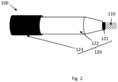
- the end section of the cable 100 is prepared for having a transition element 300, such as a joint or termination assembly mounted over it. This is done according to known techniques. For example, these surfaces may be prepared using a designated tool, sanding, glassing, etc. Typical examples of peeling & stripping tools are the CP series from Hivotec and the AMSI from Alroc. See also the co-pending application "method to minimize roughness on cable end insulation surfaces". In other words, for a certain distance, the outer semiconducting layer 123 and other outer layers (over the outer semiconducting layer), as well as some of the insulation layer 122 are removed. This provides an uncovered insulation layer surface 125 on the end section of the cable 100.
- a second cable 200 comprises an electric conductor 210 and an insulation system 220 surrounding the electric conductor 210, the insulation system 220 comprising an inner semiconducting layer 221, an insulating layer 222 and an outer semiconducting layer 223.
- Other layers, such as sheathing, water barriers... may also be present on the cable.
- the end section of the second cable 200 is prepared using the same or a similar method as for the first cable 100; also yielding an uncovered insulation layer surface 225 on the end section of the second cable 200.
- this method does not allow for a proper characterization of the uncovered insulation layer surface 125;225 that is not user dependent.
- Contact profilometry such as 2d-profilometry comprising a needle stylus dragging the surface, may in principle be used on the uncovered insulation layer surface 125;225 but this method may scratch the surface itself and may not detect the full attributes of the uncovered insulation layer surface 125;225.
- Different types of optical profilometry use light sources and are able to scan the surface topography in 3D.
- a semi portable or portable optical profilometer suitable for scanning the surface of a cable (2D and 3D surface measurement) is provided, for example the Jr25 from Nanovea.
- the suitable profilometer preferably provides a sufficient resolution that will reveal most of the micro texture, typically resolution around ⁇ m level.
- Each pixel corresponds preferably to less than 10 ⁇ m 2 , more preferably less than 5 ⁇ m 2 or even more preferably less than 1 ⁇ m 2 .
- Height wise accuracy is preferably below 50 nm, more preferably below 10 nm, even more preferably below 1 nm.
- the optical profilometer is placed directly on the lateral surface of the uncovered insulation layer surface 125;225 of the cable 100;200, at a distance from the newly exposed insulation surface suitable for scanning (depends on the instrument).
- the lateral surface of the insulation layer of the cable is scanned, obtaining measurement data, namely the surface height distribution as a function of the position (x,y), (Z(x,y)).
- scan area for each point may vary from 5x5 micrometer to 50x50 cm, the upper bound being only limited by the huge amount of data that can be processed in a timely manner.
- the scan resolution (distance between each datapoint in the measurement) may preferably vary from 5 nm steps to 5 ⁇ m steps.
- An end section of a cable 100;200 may contain several meters of uncovered insulation layer surface 125;225.
- the area of interest for analysis is the 1m section closest to the section where the electric conductor 110;210 is exposed.
- the measurement is then repeated 1 to 50 times, preferably 2 to 30 times , preferably 5 to 20 times, preferably about 10 times within the area of interest as spot measurements at randomly selected locations and/or on areas which appear less glossy to the naked eye.
- Sa ⁇ a Z x y 2 dxdy
- Sa and Sq parameters, in m are useful for comparing the height in the surface texture.
- A is the area of the measurement domain in m 2
- Lx and Ly are respectively the x and y length of the investigated domain in m.
- the Sdq parameter thus quantifies the steepness in the surface texture (i.e.
- the surface roughness of the uncovered insulation layer surface 125;225 is measured using optical profilometry as explained above (see also ISO 25178), and Sdq and/or Sa values are calculated for the uncovered insulation layer surface 125;225. These values are compared to reference values, to determine if the quality of the surface is sufficient to proceed further with preparing a cable transition.
- the measurement data may also be stored for future reference, which can be traced back if any deviations occur for the particular cable accessory during its 40-years lifetime.
- the cable end may then be transitioned, e.g. jointed to another cable end or termination, using known methods.
- the method of preparing a cable end is particularly relevant for transitions involving a physical interface, in particular for method using a pre-molded transition element 300, such as a pre-molded joint or a pre-molded termination assembly.
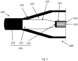
- the pre-molded transition element 300 typically comprises an electric transition element to connect the electric conductor 110;210 to a further conductor element and an insulation system surrounding the electric transition element 310, the insulation system comprising an inner semiconducting layer 321, an insulating layer 322 and an outer semiconducting layer 323.
- the electric transition element may for example be a ferrule or any other suitable element known in the art.
- a physical interface here refers to an interface between to solid surfaces, for example between a surface of a cable end and a pre-molded joint
- a chemical interface refers to a interface between a surface of a cable end and a non-solid surface, for example a melted insulation layer extruded on top of the cable end.
- the physical interface is the interface between the uncovered insulation layer surface 125;225 of the cable 100;200 and the inner surface of the insulating layer 321 of the transition element 300.
- a sample may be taken from the uncovered insulation layer surface 125;225 of the cable adjacent to the uncovered insulation layer surface 125;225 in the area to be transitioned and analyzed offsite.
- a surface sample of the insulation surface from an area adjacent to the insulation surface going into the jointing accessory is cut, for example using a knife.
- This sample can be a cut cable section of length 1 to 500 cm and a width of 1 to 20 cm, or any slap of insulation cut or machined of containing a piece of the original surface.
- This sample is sent to the offsite laboratory where the profilometer is situated. The lab may then perform the same analysis as above.
- This method may provide a standardized quality measurement providing traceable data.
- a disadvantage of this method is that the quality criteria is commonly evaluated after the joint has already been buried or installed. Whenever the quality is not considered to be satisfying, the entire cable may need to be brought up again and a new section is jointed in replacing the joint that did not meet the criteria.
Landscapes
- Processing Of Terminals (AREA)
Abstract
Description
- The present invention is within the field of surface inspection of HV cables.
- High voltage cables usually comprise an electric conductor and an insulation system surrounding the electric conductor, the insulation system comprising an inner semiconducting layer, an insulating layer and an outer semiconducting layer. High voltage can be applied with alternating current (HVAC) or direct current (HVDC).
- The quality of the joints between two HV cables is dependent on the quality of the surface at the interface between the cable and the joint, that is to say the surface of the insulation material. For these joints, a rough insulation surface has been proven to be detrimental, in that rough surfaces tend to give rise to low DC breakdown strength and thus poor performance. For AC the same rough surfaces have proved to feature similar strong field enhancement and roughness is thus detrimental for both HVAC and HVDC applications.
- As such surface quality inspection of the on-site manufactured cable insulation layer surface before jointing is important.
- Today surface quality inspection on site is carried out with the human eye, and in case of encountering deviations, regular photographs are taken. A disadvantage of a visual inspection is that it is user dependent and does not provide for a reliable and standardized quality measurement.
- Other methods for inspection of the insulation layer surface before jointing are known. However, a major disadvantage of these methods is that they require a sample to be taken from the surface and consequently damaging it. The size of the sample and the requirement of taking the sample from a part of the surface away from the cable transition area will also limit its representation of the quality of the total insulation layer surface area.
One objective of this invention is to overcome the drawbacks of the known technology. - The present invention is defined by the appended claims and in the following:
In a first aspect, the invention relates to method for preparing a cable end of a cable for transition, wherein the cable comprises an electric conductor and an insulation system surrounding the electric conductor, the insulation system comprising an inner semiconducting layer, an insulating layer and an outer semiconducting layer, the method comprising a step of: - a. removing the outer semiconducting layer and optionally part of the insulation layer, from an end section of the cable, providing an uncovered insulation layer surface on the end section of the cable;
The skilled person may use any suitable known technique for this removal step. For example these surfaces may be prepared using a designated tool, such as peeling and stripping tools, sanding, glassing, etc - b. measuring the surface roughness of the obtained uncovered insulation layer surface by optical profilometry and deriving a measured value of a roughness parameter for the uncovered insulation layer surface;
- c. comparing the measured value to a preselected reference value of the same roughness parameter; and
- if measured value is lower than the preselected reference value then the uncovered insulation layer surface has an acceptable surface quality for transition, and
- if measured value is higher than the preselected reference value for the roughness parameter then the uncovered insulation layer surface does not have an acceptable surface quality and a new uncovered insulation layer surface is prepared, and steps b and c are repeated.
- The skilled person will understand that a roughness defining parameter is any mathematical algorithm or equation that derives from the measured surface coordinates, yielding a scalar value or curve that can be used in a comparison against a reference value as an acceptance criteria. For example, amplitude parameters such as Sa, Sq, Ssk, Sku, Sp, Sv, Sz, hybrid parameters such as Sdq, Sdr, Sds, Ssc, other parameters listed in ISO 25178-2, Abott-Firestone curves, histograms, calculation of Field Enhancement Factors.
- The skilled person will understand that the measurement should be performed on a representative sample of the surface of interest, for example the measurement may be repeated 1 to 50 times, preferably 2 to 30 times , preferably 5 to 20 times, preferably about 10 times within the area of interest as spot measurements at randomly selected locations and/or on areas which appear less glossy to the naked eye.
- In an embodiment of the method, the new uncovered insulation layer surface is prepared by cutting the end section of the cable and repeating step a.
- Here the skilled person will understand that cutting the end section means cutting the part of the cable comprising the end section.
- In an embodiment of the method, the new uncovered insulation layer surface is prepared by removing part of the insulation layer, from an end section of the cable, providing a new uncovered insulation layer surface on the end section of the cable.
- In an embodiment of the method, the surface roughness of the obtained uncovered insulation layer surface measured in step b is measured in situ by use of a portable optical profilometry apparatus.
- In an embodiment of the method, the roughness parameter may be Sa.
- In an embodiment of the method, the preselected reference value for the roughness parameter Saref may be 800 nm. In another embodiment Saref may be 600 nm. In another embodiment Saref may be 400 nm. In another embodiment Saref may be 200 nm.
- In an embodiment of the method, the roughness parameter may be Sdq.
- In an embodiment of the method, the preselected reference value for the roughness parameter Sdqref may be equal to 0.8. In another embodiment Sdqref may be 0.6. In another embodiment Sdqref may be 0.4. In another embodiment Sdqref may be 0.2.
- The reference values Sdqref and Saref are selected to be the threshold values of an acceptable (or suitable) surface roughness. The skilled person will understand that these values are application dependant.
- In a second aspect, the invention relates to a method of jointing a first cable and a second cable, the first cable and the second cable comprising an electric conductor and an insulation system surrounding the electric conductor, the insulation system comprising an inner semiconducting layer, an insulating layer and an outer semiconducting layer, the method comprising the steps of:
- i. preparing an uncovered insulation layer surface at a cable end for at least one of the first and the second cables, according to the first aspect of the invention;
- ii. jointing the cable end sections.
- In an embodiment of the second aspect of the invention the uncovered insulation layer surface may be prepared at a cable end for both the first and the second cables.
- In an embodiment of the second aspect of the invention, the jointing step may be realised using a pre-molded joint.
- In a third aspect, the invention relates to a method for preparing a termination assembly on a cable, the cable comprising an electric conductor and an insulation system surrounding the electric conductor, the insulation system comprising an inner semiconducting layer, an insulating layer and an outer semiconducting layer, the method comprising the steps of:
- I. preparing an uncovered insulation layer surface at a cable end, according to the method according to the first aspect of the invention;
- II. mounting a termination assembly on the uncovered insulation layer surface.
- In a fourth aspect, the invention relates to a cable, comprising a cable end, obtainable by the method according to the first aspect of the invention.
- In a fifth aspect, the invention relates to a joint between a first and a second cable, obtainable by the method according to the second aspect of the invention.
- In a sixth aspect, the invention relates to a termination assembly on a cable, obtainable by the method according to the third aspect of the invention.
- In the following description this invention will be further explained by way of exemplary embodiments shown in the drawings:
-
Fig. 1 is a perspective view of a typical cable structure -
Fig. 2 is a perspective view a cable end prepared to be transitioned -
Fig. 3 is a side view of a cable end in a joint or termination assembly. - The quality of cable transitions, such as cable termination assemblies and joints between two HV cables is dependent on the quality of the surface at the interface between the cable and the joint, that is to say the surface of the insulation material. For these transitions, a rough insulation surface has been proven to be detrimental, in that, rough surfaces tend to give rise to low DC breakdown strength and thus poor performance. For AC the same rough surfaces have proved to feature similar strong field enhancement and roughness is thus detrimental for both HVAC and HVDC applications.
- In the preparation of a cable transition, that is to say the transition from a cable end to another element, such as in cable termination assemblies and joints, a first
electric cable 100 is provided, thefirst cable 100 comprising anelectric conductor 110 and aninsulation system 120 surrounding theelectric conductor 110, theinsulation system 120 comprising an innersemiconducting layer 121, an insulatinglayer 122 and an outersemiconducting layer 123. Other layers, such as sheathing, water barriers, etc may also be present on the cable. This cable is illustrated infigure 1 . - The end section of the
cable 100 is prepared for having atransition element 300, such as a joint or termination assembly mounted over it. This is done according to known techniques. For example, these surfaces may be prepared using a designated tool, sanding, glassing, etc. Typical examples of peeling & stripping tools are the CP series from Hivotec and the AMSI from Alroc. See also the co-pending application "method to minimize roughness on cable end insulation surfaces". In other words, for a certain distance, the outersemiconducting layer 123 and other outer layers (over the outer semiconducting layer), as well as some of theinsulation layer 122 are removed. This provides an uncoveredinsulation layer surface 125 on the end section of thecable 100. - In case of jointing, a second cable 200 is provided, the second cable 200 comprises an electric conductor 210 and an insulation system 220 surrounding the electric conductor 210, the insulation system 220 comprising an inner semiconducting layer 221, an insulating layer 222 and an outer semiconducting layer 223. Other layers, such as sheathing, water barriers... may also be present on the cable. The end section of the second cable 200 is prepared using the same or a similar method as for the
first cable 100; also yielding an uncovered insulation layer surface 225 on the end section of the second cable 200. - Today, on site surface quality inspection of the uncovered
insulation layer surface 125;225 is carried out with the human eye, and in case of encountering deviations, photographs are taken with a film or digital camera. - However, this method does not allow for a proper characterization of the uncovered
insulation layer surface 125;225 that is not user dependent. - It is proposed here to use profilometry to characterize the uncovered
insulation layer surface 125;225. - Contact profilometry, such as 2d-profilometry comprising a needle stylus dragging the surface, may in principle be used on the uncovered
insulation layer surface 125;225 but this method may scratch the surface itself and may not detect the full attributes of the uncoveredinsulation layer surface 125;225.
Different types of optical profilometry use light sources and are able to scan the surface topography in 3D. - It is possible to extract samples from the
insulation layer 122 of the cable end, close to the area that will be part of the cable transition, but not in it. These sample may then be brought to the lab for profilometry. However, even though this method is advantageous, taking these samples is a destructive method and introduces time lag between cable transition creation and inspection completion. - Recent progress in optical profilometry have yielded portable optical profilometer that allow for the measurement to be done in the field, avoiding taking a sample, skipping the time lag, allowing for an on-site characterization of the uncovered
insulation layer surface 125;225, even before making the cable transition, e.g. a joint or a termination assembly, allowing for possible improvement of the uncoveredinsulation layer surface 125;225. - A semi portable or portable optical profilometer suitable for scanning the surface of a cable (2D and 3D surface measurement) is provided, for example the Jr25 from Nanovea. The suitable profilometer preferably provides a sufficient resolution that will reveal most of the micro texture, typically resolution around µm level. Each pixel corresponds preferably to less than 10 µm2, more preferably less than 5 µm2 or even more preferably less than 1 µm2. Height wise accuracy is preferably below 50 nm, more preferably below 10 nm, even more preferably below 1 nm.
- Then the optical profilometer is placed directly on the lateral surface of the uncovered
insulation layer surface 125;225 of thecable 100;200, at a distance from the newly exposed insulation surface suitable for scanning (depends on the instrument). The lateral surface of the insulation layer of the cable is scanned, obtaining measurement data, namely the surface height distribution as a function of the position (x,y), (Z(x,y)). - Preferably, scan area for each point may vary from 5x5 micrometer to 50x50 cm, the upper bound being only limited by the huge amount of data that can be processed in a timely manner.
- The scan resolution (distance between each datapoint in the measurement) may preferably vary from 5 nm steps to 5 µm steps.
- An end section of a
cable 100;200 may contain several meters of uncoveredinsulation layer surface 125;225. The area of interest for analysis is the 1m section closest to the section where theelectric conductor 110;210 is exposed. - The measurement is then repeated 1 to 50 times, preferably 2 to 30 times , preferably 5 to 20 times, preferably about 10 times within the area of interest as spot measurements at randomly selected locations and/or on areas which appear less glossy to the naked eye.
- Features in the surface texture can be quantified using roughness parameters, which represent features in a certain measurement domain with a single parameter value, thus facilitating direct comparisons of certain surface types. The average roughness (or arithmetical mean height variation) of a certain 3D surface is quantified through Sa, expressed as:


- Sa and Sq parameters, in m, are useful for comparing the height in the surface texture. However, two surface types having identical Sa and Sq parameter values can have vastly different textures, as the texture's spacing can be present with different widths. Therefore, a third parameter, the unitless RMS surface slope Sdq, is introduced as:

- The surface roughness of the uncovered
insulation layer surface 125;225 is measured using optical profilometry as explained above (see also ISO 25178), and Sdq and/or Sa values are calculated for the uncoveredinsulation layer surface 125;225. These values are compared to reference values, to determine if the quality of the surface is sufficient to proceed further with preparing a cable transition. - if Sdq < Sdqref or Sa < Saref, then the uncovered
insulation layer surface 125;225 has a satisfying surface quality and the cable transition may be further prepared, - if Sdq > Sdqref and/or Sa > Saref, then the uncovered
insulation layer surface 125;225 does not have a satisfying surface quality. A new surface may be prepared using known methods, or the prepared cable end may be cut and a new cable end may be prepared. - The measurement data may also be stored for future reference, which can be traced back if any deviations occur for the particular cable accessory during its 40-years lifetime.
- When the cable end meets the quality criteria, the cable end may then be transitioned, e.g. jointed to another cable end or termination, using known methods. The method of preparing a cable end is particularly relevant for transitions involving a physical interface, in particular for method using a
pre-molded transition element 300, such as a pre-molded joint or a pre-molded termination assembly.
Thepre-molded transition element 300 typically comprises an electric transition element to connect theelectric conductor 110;210 to a further conductor element and an insulation system surrounding theelectric transition element 310, the insulation system comprising an innersemiconducting layer 321, an insulatinglayer 322 and an outersemiconducting layer 323. - In a joint, the electric transition element may for example be a ferrule or any other suitable element known in the art.
- The skilled person will understand here that a physical interface here refers to an interface between to solid surfaces, for example between a surface of a cable end and a pre-molded joint, whereas a chemical interface refers to a interface between a surface of a cable end and a non-solid surface, for example a melted insulation layer extruded on top of the cable end. Here the physical interface is the interface between the uncovered
insulation layer surface 125;225 of thecable 100;200 and the inner surface of the insulatinglayer 321 of thetransition element 300. - The obtained physical interface, between a cable end and a pre-molded joint or a pre-molded termination assembly is illustrated in
figure 3 . - This specific procedure creates a fool-proof quality control of insulation roughness introduced into high voltage cable accessories, such as any kind of joint or termination assembly. Also full traceability is gained over quality of work for all installations for each specific cable project. Ensuring that roughness levels, and thus the level of local field enhancement is below a certain value, is detrimental for guaranteeing that locally enhanced ageing rates may be present and that the accessory will last its specified life time without break down of the insulation system.
- When it is not possible to perform the analysis on site, or when it is preferable to analyze a series of samples on an offsite laboratory, a sample may be taken from the uncovered
insulation layer surface 125;225 of the cable adjacent to the uncoveredinsulation layer surface 125;225 in the area to be transitioned and analyzed offsite. - A surface sample of the insulation surface from an area adjacent to the insulation surface going into the jointing accessory is cut, for example using a knife. This sample can be a cut cable section of length 1 to 500 cm and a width of 1 to 20 cm, or any slap of insulation cut or machined of containing a piece of the original surface. This sample is sent to the offsite laboratory where the profilometer is situated. The lab may then perform the same analysis as above.
- This method may provide a standardized quality measurement providing traceable data. However, a disadvantage of this method is that the quality criteria is commonly evaluated after the joint has already been buried or installed. Whenever the quality is not considered to be satisfying, the entire cable may need to be brought up again and a new section is jointed in replacing the joint that did not meet the criteria.
Claims (15)
- A method for preparing a cable end of a cable (100, 200) for transition, wherein the cable (100, 200) comprises an electric conductor (110, 210) and an insulation system (120, 220) surrounding the electric conductor (110, 210), the insulation system (120, 220) comprising an inner semiconducting layer (121, 221), an insulating layer (122, 222) and an outer semiconducting layer (123, 223), the method comprising a step of:a. removing the outer semiconducting layer (123, 223) and optionally part of the insulation layer (122, 222), from an end section of the cable (100, 200), providing an uncovered insulation layer surface (125,225) on the end section of the cable (100, 200); andb. measuring the surface roughness of the obtained uncovered insulation layer surface (125,225) by optical profilometry and deriving a measured value of a roughness parameter for the uncovered insulation layer surface (125,225);c. comparing the measured value to a preselected reference value of the same roughness parameter; and- if measured value is lower than the preselected reference value then the uncovered insulation layer surface (125,225) has an acceptable surface quality for transition, or- if measured value is higher than the preselected reference value for the roughness parameter then the uncovered insulation layer surface (125,225) does not have an acceptable surface quality, a new uncovered insulation layer surface (125,225) is prepared, and step b and c are repeated.
- A method according to claim 1, wherein the new uncovered insulation layer surface (125,225) is prepared by cutting the end section of the cable (100;200) and repeating step a.
- A method according to claim 1, wherein the new uncovered insulation layer surface (125,225) is prepared by removing part of the insulation layer (122, 222), from an end section of the cable (100, 200), providing an new uncovered insulation layer surface (125,225) on the end section of the cable (100, 200).
- A method according to anyone of the previous claims, wherein the surface roughness of the obtained uncovered insulation layer surface (125,225) measured in step b is measured in situ by use of a portable optical profilometry apparatus.
- A method according to anyone of the previous claims, wherein the roughness parameter is Sa.
- A method according to claim 5, wherein the preselected reference value for the roughness parameter Saref = 800 nm.
- A method according to anyone of the previous claims, wherein the roughness parameter is Sdq.
- A method according to claim 7, wherein the preselected reference value for the roughness parameter Sdqref = 0.8.
- A method of jointing a first cable (100) and a second cable (200), the first cable (100) and the second cable (200) comprising an electric conductor (110, 210) and an insulation system (120, 220) surrounding the electric conductor (110, 210), the insulation system (120, 220) comprising an inner semiconducting layer (121, 221), an insulating layer (122,222) and an outer semiconducting layer (123,223), the method comprising the steps of:i. preparing an uncovered insulation layer surface (125,225) at an end section of at least one of the first cable (100) and the second cable (200), by use of the method according to anyone of the previous claims;ii. jointing the end sections of the first cable (100) and the second cable (200).
- A method of jointing a first cable (100) and a second cable (200), according to claim 9 wherein an uncovered insulation layer surface (125, 225) is prepared at an end section of both the first and the second cables (100, 200).
- A method of jointing a first cable (100) and a second cable (200), according to claim 10, wherein the jointing step is realised using a pre-molded joint.
- A method for preparing a termination assembly on a cable (100, 200), the cable comprising an electric conductor (110, 210) and an insulation system (120, 220) surrounding the electric conductor (110, 210), the insulation system (120, 220) comprising an inner semiconducting layer (121, 221), an insulating layer (122,222) and an outer semiconducting layer (123,223), the method comprising the steps of:I. preparing an uncovered insulation layer surface (125,225) at an end section of the cable, by use of the method according to anyone of claims 1-8;II. mounting a termination assembly on the uncovered insulation layer surface (125,225).
- A cable (100, 200), comprising an end section, obtainable by the method according to anyone of claims 1 to 8.
- A joint between a first and a second cable (100, 200) obtainable by the method according to anyone of claims 9 to 11.
- A termination assembly on a cable (100, 200) obtainable by the method according to claim 12.
Priority Applications (2)
| Application Number | Priority Date | Filing Date | Title |
|---|---|---|---|
| EP21306532.9A EP4175085A1 (en) | 2021-10-29 | 2021-10-29 | Optical profilometry on hv cable ends and on samples extracted form hv cables |
| US17/973,363 US12531400B2 (en) | 2021-10-29 | 2022-10-25 | Optical profilometry on hv cable ends and on samples extracted form hv cables |
Applications Claiming Priority (1)
| Application Number | Priority Date | Filing Date | Title |
|---|---|---|---|
| EP21306532.9A EP4175085A1 (en) | 2021-10-29 | 2021-10-29 | Optical profilometry on hv cable ends and on samples extracted form hv cables |
Publications (1)
| Publication Number | Publication Date |
|---|---|
| EP4175085A1 true EP4175085A1 (en) | 2023-05-03 |
Family
ID=78617356
Family Applications (1)
| Application Number | Title | Priority Date | Filing Date |
|---|---|---|---|
| EP21306532.9A Pending EP4175085A1 (en) | 2021-10-29 | 2021-10-29 | Optical profilometry on hv cable ends and on samples extracted form hv cables |
Country Status (2)
| Country | Link |
|---|---|
| US (1) | US12531400B2 (en) |
| EP (1) | EP4175085A1 (en) |
Cited By (2)
| Publication number | Priority date | Publication date | Assignee | Title |
|---|---|---|---|---|
| EP4518057A1 (en) | 2023-08-31 | 2025-03-05 | Nexans | Flexible joint for power cable |
| NO20231312A1 (en) * | 2023-12-04 | 2025-06-05 | Nexans | Method for controlling the quality of a transition surface of a high voltage electric component for a transition |
Citations (1)
| Publication number | Priority date | Publication date | Assignee | Title |
|---|---|---|---|---|
| JPH06178422A (en) * | 1992-12-07 | 1994-06-24 | Sumitomo Densetsu Kk | Automatic stripping apparatus for cable semiconductor layer |
Family Cites Families (10)
| Publication number | Priority date | Publication date | Assignee | Title |
|---|---|---|---|---|
| JP3700913B2 (en) * | 1998-11-12 | 2005-09-28 | 古河電気工業株式会社 | Power cable terminal processing method |
| JP4346601B2 (en) * | 2005-10-28 | 2009-10-21 | 株式会社ビスキャス | Cutting method of outer semiconductive layer of power cable |
| CN103563198B (en) * | 2011-06-08 | 2017-05-24 | Abb研究有限公司 | Laser processed conductive substrate and method of pretreatment thereof |
| EP3207600B1 (en) * | 2014-10-15 | 2019-01-30 | Rittal GmbH & Co. KG | Cable sequence for a wiring of an electrical circuit, method for production and use |
| JP6959774B2 (en) * | 2017-07-04 | 2021-11-05 | 日立金属株式会社 | Signal transmission cable Multi-core cable and signal transmission cable manufacturing method |
| JP6245402B1 (en) * | 2017-07-04 | 2017-12-13 | 日立金属株式会社 | Differential signal transmission cable, multi-core cable, and differential signal transmission cable manufacturing method |
| EP3900132A1 (en) * | 2018-12-21 | 2021-10-27 | 3M Innovative Properties Company | Electrical power cable preparation system |
| JP7172639B2 (en) * | 2019-01-22 | 2022-11-16 | 日立金属株式会社 | Linear member and its manufacturing method |
| WO2020206627A1 (en) * | 2019-04-10 | 2020-10-15 | 3M Innovative Properties Company | Cable preparation inspection device, system and method |
| EP3916937A1 (en) * | 2020-05-29 | 2021-12-01 | Nexans | Conductor joint |
-
2021
- 2021-10-29 EP EP21306532.9A patent/EP4175085A1/en active Pending
-
2022
- 2022-10-25 US US17/973,363 patent/US12531400B2/en active Active
Patent Citations (1)
| Publication number | Priority date | Publication date | Assignee | Title |
|---|---|---|---|---|
| JPH06178422A (en) * | 1992-12-07 | 1994-06-24 | Sumitomo Densetsu Kk | Automatic stripping apparatus for cable semiconductor layer |
Non-Patent Citations (1)
| Title |
|---|
| DOEDENS ESPEN ET AL: "Space Charge Accumulation at Material Interfaces in HVDC Cable Insulation Part I-Experimental Study and Charge Injection Hypothesis", ENERGIES, vol. 13, no. 8, 17 April 2020 (2020-04-17), pages 2005, XP055910067, DOI: 10.3390/en13082005 * |
Cited By (4)
| Publication number | Priority date | Publication date | Assignee | Title |
|---|---|---|---|---|
| EP4518057A1 (en) | 2023-08-31 | 2025-03-05 | Nexans | Flexible joint for power cable |
| NO20231312A1 (en) * | 2023-12-04 | 2025-06-05 | Nexans | Method for controlling the quality of a transition surface of a high voltage electric component for a transition |
| EP4567411A1 (en) | 2023-12-04 | 2025-06-11 | Nexans | Method for controlling the quality of a transition surface of a high voltage electric component for a transition |
| NO349249B1 (en) * | 2023-12-04 | 2025-11-17 | Nexans | Method for controlling the quality of a transition surface of a high voltage electric component for a transition |
Also Published As
| Publication number | Publication date |
|---|---|
| US20230132865A1 (en) | 2023-05-04 |
| US12531400B2 (en) | 2026-01-20 |
Similar Documents
| Publication | Publication Date | Title |
|---|---|---|
| US12531400B2 (en) | Optical profilometry on hv cable ends and on samples extracted form hv cables | |
| US20230411939A1 (en) | ASIT laser scanning on cable and assembly defects | |
| EP3901571A1 (en) | Surface quality determination of a high voltage cable end | |
| Kantar et al. | A stochastic model for contact surfaces at polymer interfaces subjected to an electrical field | |
| US12487189B2 (en) | Laser scanning of cable and cable accessory components subjected to mechanical loads and elastic or inelastic deformation | |
| US12560426B2 (en) | Method for inspecting surfaces and interfaces of high voltage cable components | |
| CN109444260A (en) | A kind of prediction technique of cable connector compound interface breakdown voltage | |
| US20230135919A1 (en) | Method to minimize roughness on cable end insulation surfaces | |
| US12555217B2 (en) | System and method for positioning of pre-molded accessory component for a high voltage cable | |
| US20250389674A1 (en) | Method of Quality Inspection of a Joint of a Power Cable | |
| CN115456964A (en) | Product internal flow passage molded surface extraction method based on industrial CT | |
| Angelini et al. | An imaging approach for a contactless monitoring of the conservation state of metallic works of art | |
| Ammann et al. | Characterization of self-affine surfaces from 3D digital reconstruction | |
| Kantar et al. | A stochastic model for contact surfaces at polymer interfaces considering contact pressure, elasticity and surface roughness | |
| Bordeori et al. | Water Tree Growth in XLPE Polymeric Insulation Induced by Various Types of Defects | |
| EP4567411B1 (en) | Method for controlling the quality of a transition surface of a high voltage electric component for a transition | |
| EP4582771A1 (en) | Method for manufacturing and inspecting a factory joint during installation | |
| EP4563965A1 (en) | Quality control method for a cabel specimen | |
| Ramirez-Vazquez et al. | Fractal analysis for classification of electrical testing of polymer high voltage insulators | |
| Bostrom et al. | Electrical stress enhancement of contaminants in XLPE insulation as quality control criteria | |
| Kadkhoda et al. | Pattern and form recognition of statistically distributed defects on functional optical surfaces | |
| CN115042020A (en) | Method for automatically polishing cable insulating layer | |
| CN120177412A (en) | Cable flexible joint defect detection method, device, system, equipment and storage medium | |
| CN121678738A (en) | Factory inspection system and method for normal-temperature insulating superconducting cable | |
| CN121633085A (en) | A Smart Qualitative Analysis Method and System for the Causes of Surface Protrusions in Cable Shielding Material |
Legal Events
| Date | Code | Title | Description |
|---|---|---|---|
| PUAI | Public reference made under article 153(3) epc to a published international application that has entered the european phase |
Free format text: ORIGINAL CODE: 0009012 |
|
| STAA | Information on the status of an ep patent application or granted ep patent |
Free format text: STATUS: THE APPLICATION HAS BEEN PUBLISHED |
|
| AK | Designated contracting states |
Kind code of ref document: A1 Designated state(s): AL AT BE BG CH CY CZ DE DK EE ES FI FR GB GR HR HU IE IS IT LI LT LU LV MC MK MT NL NO PL PT RO RS SE SI SK SM TR |
|
| STAA | Information on the status of an ep patent application or granted ep patent |
Free format text: STATUS: REQUEST FOR EXAMINATION WAS MADE |
|
| 17P | Request for examination filed |
Effective date: 20231103 |
|
| RBV | Designated contracting states (corrected) |
Designated state(s): AL AT BE BG CH CY CZ DE DK EE ES FI FR GB GR HR HU IE IS IT LI LT LU LV MC MK MT NL NO PL PT RO RS SE SI SK SM TR |