EP4175079A1 - Method of fabrication of region with regulary varying refractive index in a layered semiconductor structure - Google Patents
Method of fabrication of region with regulary varying refractive index in a layered semiconductor structure Download PDFInfo
- Publication number
- EP4175079A1 EP4175079A1 EP22461628.4A EP22461628A EP4175079A1 EP 4175079 A1 EP4175079 A1 EP 4175079A1 EP 22461628 A EP22461628 A EP 22461628A EP 4175079 A1 EP4175079 A1 EP 4175079A1
- Authority
- EP
- European Patent Office
- Prior art keywords
- ion implantation
- mask
- etching
- subjected
- refractive index
- Prior art date
- Legal status (The legal status is an assumption and is not a legal conclusion. Google has not performed a legal analysis and makes no representation as to the accuracy of the status listed.)
- Granted
Links
Images

Classifications
-
- H—ELECTRICITY
- H01—ELECTRIC ELEMENTS
- H01S—DEVICES USING THE PROCESS OF LIGHT AMPLIFICATION BY STIMULATED EMISSION OF RADIATION [LASER] TO AMPLIFY OR GENERATE LIGHT; DEVICES USING STIMULATED EMISSION OF ELECTROMAGNETIC RADIATION IN WAVE RANGES OTHER THAN OPTICAL
- H01S5/00—Semiconductor lasers
- H01S5/10—Construction or shape of the optical resonator, e.g. extended or external cavity, coupled cavities, bent-guide, varying width, thickness or composition of the active region
- H01S5/12—Construction or shape of the optical resonator, e.g. extended or external cavity, coupled cavities, bent-guide, varying width, thickness or composition of the active region the resonator having a periodic structure, e.g. in distributed feedback [DFB] lasers
- H01S5/1231—Grating growth or overgrowth details
-
- G—PHYSICS
- G02—OPTICS
- G02B—OPTICAL ELEMENTS, SYSTEMS OR APPARATUS
- G02B5/00—Optical elements other than lenses
- G02B5/18—Diffraction gratings
- G02B5/1861—Reflection gratings characterised by their structure, e.g. step profile, contours of substrate or grooves, pitch variations, materials
-
- H—ELECTRICITY
- H10—SEMICONDUCTOR DEVICES; ELECTRIC SOLID-STATE DEVICES NOT OTHERWISE PROVIDED FOR
- H10P—GENERIC PROCESSES OR APPARATUS FOR THE MANUFACTURE OR TREATMENT OF DEVICES COVERED BY CLASS H10
- H10P50/00—Etching of wafers, substrates or parts of devices
- H10P50/60—Wet etching
- H10P50/61—Electrolytic etching
- H10P50/617—Electrolytic etching of Group III-V materials
Definitions
- the present invention relates to a method of fabrication of a region with a regularly variable refractive index in a selected layer of a layered semiconductor structure fabricated epitaxially of group-III nitrides on a crystalline substrate.
- the embedded layers with a regularly variable refractive index which are located inside the semiconductor structure, are known in the technology of fabrication of some semiconductor optoelectronic devices, for example laser diodes.
- a mask is fabricated by the lithography method on a selected semiconductor layer, and subsequently dry etching method is used to make grooves or openings in said layer, and subsequently another layer of a material with a different refractive index than that of the material of the layer with the grooves is applied.
- fabricated periodic photonic structure is integrated monolithically, epitaxially with the device structure. Fabrication of such photonic structures inside optoelectronic devices is disclosed in EP1094345A1 .
- Another advantage of placing a diffraction grating on the top surface is that the contrast between GaN and air is much higher than between GaN and its alloys with indium or aluminium.
- the refractive index for the wavelength of 450 nm is 2.45 for GaN, 2.40 for AlGaN with 8% Al content, and 1 for air.
- Examples of devices with a photonic grating on the surface are disclosed in EP3767762A1 , US6671306B1 , US4722092A and US4777148A .
- a dielectric layer which blocks the further epitaxial growth, is applied to the lower surface of such an opening.
- the openings were overgrown in the re-growth process to form an ordered network of empty spaces filled with air and the remaining dielectric layer.
- this approach poses a risk of defects at the place of coalescence of the opening edges during the overgrowth.
- a change in the electric properties of semiconductors through ion implantation is well known.
- An example of a detailed description of implantation doping of GaN is presented in US9984881 B2 . In this document, selective area doping is applied to fabricate an ohmic contact. Selected areas are masked before ion implantation.
- n-type conductivity a desired change in electric properties, namely n-type conductivity, using implantation doping of group III nitrides requires thermal activation, often after appropriate covering the surface to prevent its decomposition. It is proved that n-type doping of GaN is possible with the use of Si or Ge ion implantation and subsequent high temperature annealing.
- selective removal of an epitaxial n-type doped layer through electrochemical etching of group III nitrides is known.
- a method of selective removal of certain n-type conductivity layers of GaN with a higher concentration of dopants than in the other GaN layers in the same structure is disclosed for example in US10458038B2 .
- the goal of the invention is providing an effective method of fabrication of a volume with a regularly and strongly variable refractive index in a plane that is parallel to the substrate, in a selected layer of the layered semiconductor structure.
- This goal is achieved by the method according to the invention, wherein after fabricating a selected epitaxial layer the growth process is interrupted and a mask that locally blocks the ion implantation is placed on the top surface of the fabricated structure.
- Said mask contains an array of longitudinal windows with the same width, which are parallel to each other and distributed at an equal spacing.
- the upper epitaxial layer is subjected to the ion implantation process with the use of germanium or silicon ions, to the depth that is not greater than the thickness of the upper epitaxial layer and to the concentration of the implanted atoms that is higher than 5 ⁇ 10 18 cm -3 .
- the mask is removed and, if necessary, the epitaxial growth of the structure is finished.
- the epitaxial structure is annealed at a temperature from 1000 to 1400°C, for a period between ten seconds and one hour.
- the mask is made in the process of electron-beam lithography or photolithography.
- the width of the windows in the mask ranges from 25 to 1750 nm, while the sum of the window width and a spacing between the window edges ranges from 50 to 3000 nm.
- oxalic acid and voltage ranging from 2 to 15 V are used for the electrochemical etching of the areas subject to the ion implantation.
- the etching of the volumes that were subjected to the ion implantation is carried out until the empty air channel spaces formed as a result of said etching are reached, with the length that is at least equal to the width of the mesa of the optoelectronic device in which the fabricated volume with a regularly variable refractive index will be used.
- the invention breaks the commonly accepted opinion among specialists that a low refractive index contrast and the large lattice mismatch of nitride materials are fundamental obstacles in fabrication of photonic structures embedded inside the GaN based device structures.
- a photonic element fabricated according to the invention does not use bulk materials such as GaN and AlGaN in the growth process, in which defects can be generated due to the different lattice constants, but for fabricating an ordered array of empty channel spaces a crystalline layer of GaN and air are used, thus eliminating the problem of lattice mismatch, at the same time ensuring a high contrast of the refractive indices.
- the application of the invention is possible also in other fields than optoelectronics, for example micro- or nanofluidics for fabricating a system of empty channels with an arbitrary layout in GaN, and for examining micro- and nanoflows.
- optoelectronics for example micro- or nanofluidics for fabricating a system of empty channels with an arbitrary layout in GaN, and for examining micro- and nanoflows.
- There are a few very important advantages of the invention namely preservation of a flat upper surface for the subsequent epitaxial processes, a perfect epitaxial relation with the whole structure, and good electrical and thermal conductivity, which are of key importance in the structure of optoelectronic devices.
- Preservation of a flat surface above the empty air channels ensures a uniform thickness of the quantum wells grown epitaxially on top and facilitates applying metal contacts.
- the invention makes it possible to place an array of air channels under the group-III nitride structure surface, in a close proximity to the active region, less than 300 nm, which is necessary for ensuring a strong coupling of the diffraction grating with the optical mode of the optoelectronic device, for example in distributed feedback laser diodes.
- the invention can be applied both during the process of epitaxial growth of the device structure and after its end. It also provides a freedom of selection of the layout of the air channels geometry, depending on the applied implantation parameters and the selected mask fabrication technique, in particular giving the possibility to obtain periodicity of the refractive index ranging from 50 to 3500 nm. Fabrication of empty air channels through electrochemical etching is an uncomplicated and non-toxic process.
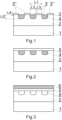
- FIG.1 An embodiment of the invention is shown schematically in a drawing, with Fig.1 presenting a vertical profile of a nitride epitaxial structure after the mask fabrication and the ion implantation of selected areas, Fig.2 presenting the structure from Fig.1 after removing the mask and another epitaxial layer growth, and Fig.3 presenting the structure from Fig.2 after etching the areas that were subjected to the ion implantation.
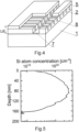
- Fig.4 presents an axonometric view of the structure from Fig. 3 with the visible layout of the groove for the etching medium.
- Fig.5 presents a theoretically calculated profile of silicon ion implantation as a function of depth, which was applied in the embodiment.
- Fig.6 shows a top view of the surface of an embodiment of the epitaxial structure described below, after its electrochemical etching, imaged with the use of an optical microscope.
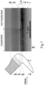
- Fig.7 presents a photograph taken by a scanning electron microscope of the vertical profile of the final nitride structure after the etching process reflected in a similar view as in Fig.3 , where the non-implanted place remained non-etched, while an empty air channels fabricated in the etching process is visible at the position which was previously subjected to the ion implantation.
- the invention is presented in more detail in the embodiment, described below, of fabrication of an epitaxial substrate with a regularly variable refractive index in the first layer epitaxially grown on the crystalline substrate, on which another epitaxial layer is grown, which substrate is suitable (with appropriately decreased mask period), among others, for fabricating distributed feedback laser diodes.
- a GaN layer 2 with the thickness of 650 nm was applied to the gallium nitride crystalline substrate 1 in the process of plasma assisted molecular beam epitaxy (PAMBE).
- PAMBE plasma assisted molecular beam epitaxy
- a mask 3 intended to locally block the ion implantation, was made by photolithography according to a known method on the upper surface of the layer 2.
- the mask 3 contained an array of windows 3' with the width L2 of 4.5 ⁇ m, which were parallel to each other and separated from each other by implantation blocking mesas 3" with the width L3 of 3.5 ⁇ m.
- the sum of the widths L2 and L3 gives the periodicity L1 of the regions with a variable refractive index.
- the thickness L4 of the created mask 3 was 1.2 ⁇ m.
- the ion implantation was performed according to a known method with the use of silicon ions with the energy of 100 keV with the dose of 2.6 ⁇ 10 15 cm -2 , to the depth L5 of 170 nm.
- regions 4 containing implanted silicon atoms were obtained.
- a depth profile of the concentration of said atoms is reflected in the diagram in Fig.5 .
- Said diagram reveals that the maximum concentration of atoms in the volume of the regions 4 was 3 ⁇ 10 20 cm -3 at the depth of 76 nm.
- the mask 3 was removed and a GaN layer 5 with the thickness of 100 nm was applied in the same epitaxial growth process as before, and subsequently the obtained layer structure was annealed for 5 minutes at the temperature of 1070°C.
- a protective layer which is not reflected in the drawing, made of for example silicon nitride, silicon oxide, aluminium nitride or a combination thereof, for the purpose of protecting the upper surface of the layer 5 from decomposition during the annealing.
- a covering layer 6 with the thickness of 500 nm made of silicon oxide SiOz was applied according to a known method for the purpose of blocking the access of the etching medium from the top, after which a groove 7 was made for the etching medium with the thickness L6 of 220 nm and the width of 5 ⁇ m.
- the groove 7 was made according to the known method of dry etching, i.e. through reactive ion etching in chlorine-argon plasma.
- electrochemical etching was carried out in a 0.3 mol oxalic acid solution with the voltage of 8 V and for the period of 120 minutes.
- the etching time can be chosen freely, in particular such that the length L7 ( Fig.6 ) of the empty air channels 8 corresponds to the subsequent planned layout of the optoelectronic device fabricated on a substrate with a regularly variable refractive index, in particular such that the length L7 is greater than the width of the laser mesa.
- the control of the etching process of the regions 4 was carried out with the use of an optical microscope. Due to a strong change in the refractive index of the etched volume, a contrast was visible under the microscope at places where as a result of said etching the air channels 8 were formed. This is visible well in Fig.6 , where the lower surface of the groove 7 for the etching medium is visible.
- the channel spaces 8 located under the surface of the epitaxial structure covered by a covering layer 6 from the top are visible in the top view as brighter ones due to the considerably reduced locally refractive index compared to the non-implanted and non-etched areas in the layer 2.
- the length L7 of the empty air channels 8 obtained after the aforementioned etching period of 120 minutes was estimated to be 15 ⁇ m on average based on the photographs from the optical microscope.
- Fig.7 presents an image of the structure after the electrochemical etching obtained with the use of a scanning electron microscope (SEM), after inclining it by 45 degrees, where the wall of the etching medium groove, containing the covering layer 6, the layer 5 and the layer 2, is visible in the central part.
- the profile counted from the upper surface of the layer 5 in the direction of the crystalline substrate 1 has the depth L6, which is 220 nm in the described embodiment.
- the image shown in Fig.7 proves that an empty air channel 8 is visible at the position which was previously subjected to silicon ion implantation (4), while the non-implanted areas remains unchanged.
- FIG.3 presents illustratively a schematic axonometric view of the structure with a system of periodically distributed air channels with the visible layout of an opening for the etching medium 7 after removing the covering layer 6.
- a part of the layer 5 is not shown illustratively in order to make the layout of the channels inside the structure visible.
- the invention can be implemented also where a different epitaxial technique is used for applying the layer 2 or where the ion implantation is carried out directly to the GaN substrate.
- the mask 3 can be made also with the use of the known electron-beam lithography, which allows obtaining a shorter periodicity L1 providing a better coupling with the optical mode where the invention is applied for fabricating structures of distributed feedback laser diodes.
- the mask 3 is designed taking into account the wavelength of the final device.
- the optimum period L1 for lasers emitting light with the wavelength of 450 nm ranges from 50 to 3500 nm.
- the width L2 of the windows 3' in the mask 3 should range from 25 to 1750 nm.
- the surface of the windows 3' in the mask 3 for the electron-beam lithography or photolithography occupies between 5 and 60% of the whole surface of the mask 3.
- the mask thickness must be selected such that it locally blocks the ions being implanted.
- a mask composed of a layer of silicon oxide SiOz with the thickness of 250 nm and a layer of chromium with the thickness of 20 nm effectively blocks silicon ions with the energy of 100 keV.
Landscapes
- Physics & Mathematics (AREA)
- Condensed Matter Physics & Semiconductors (AREA)
- General Physics & Mathematics (AREA)
- Electromagnetism (AREA)
- Optics & Photonics (AREA)
- Semiconductor Lasers (AREA)
- Crystals, And After-Treatments Of Crystals (AREA)
Abstract
Description
- The present invention relates to a method of fabrication of a region with a regularly variable refractive index in a selected layer of a layered semiconductor structure fabricated epitaxially of group-III nitrides on a crystalline substrate.
- The embedded layers with a regularly variable refractive index, which are located inside the semiconductor structure, are known in the technology of fabrication of some semiconductor optoelectronic devices, for example laser diodes. Most often, for the purpose of obtaining such a volume, a mask is fabricated by the lithography method on a selected semiconductor layer, and subsequently dry etching method is used to make grooves or openings in said layer, and subsequently another layer of a material with a different refractive index than that of the material of the layer with the grooves is applied. Thus fabricated periodic photonic structure is integrated monolithically, epitaxially with the device structure. Fabrication of such photonic structures inside optoelectronic devices is disclosed in
EP1094345A1 . The possibility to implement this concept in nitrides of group III metals is presented for example in the paper by D.Hofstetter, RL Thornton, LT Romano, DP Bour, M. Kneissl & RM Donaldson titled "Roomtemperature pulsed operation of an electrically injected InGaN/GaN multi-quantum well distributed feedback laser" [Applied Physics Letters 73, 2158-2160 (1998)]. It describes a diffraction grating located inside the structure and integrated monolithically with said structure. Unfortunately, such a solution cannot be used routinely in group-III nitrides for the fabrication of photonic elements inside the structures based on group-III nitrides, because gallium nitride (GaN) and its alloys with indium and aluminium are characterised by a low contrast of the refractive index and a large lattice mismatch. These two features constitute a fundamental obstacle in fabrication of a high quality of buried photonic structures unlike in the case of group III arsenides and group III phosphides. Therefore, photonic gratings in devices based on group III nitrides are usually formed on the top surface. Another advantage of placing a diffraction grating on the top surface is that the contrast between GaN and air is much higher than between GaN and its alloys with indium or aluminium. For example, the refractive index for the wavelength of 450 nm is 2.45 for GaN, 2.40 for AlGaN with 8% Al content, and 1 for air. Examples of devices with a photonic grating on the surface are disclosed inEP3767762A1 ,US6671306B1 ,US4722092A andUS4777148A . A different approach to fabrication of a diffraction grating embedded inside a semiconductor structure is presented on the example of a structure based on group III arsenides inUS6365428B1 , which discloses the use of lateral oxidation of components of the diffraction grating placed inside the structure, which components were made previously in the process of lithography of an appropriate pattern, dry etching and re-epitaxy. Exposure of the AlAs layer side surface and its lateral oxidation causes a considerable increase in the refractive index contrast between the materials forming the diffraction grating. A similar solution is disclosed inUS6649439B1 , which presents a method of periodic distribution of a dielectric inside the structure obtained in the re-growth process. A further increase in the contrast between the materials forming the diffraction grating is possible through selective removal of the dielectric layer, which leads to obtaining empty spaces. Both solutions described above are applied in devices based on group III arsenides and group III phosphides. A similar demonstration in the material system of group III nitrides is presented in the paper by H. Matsubara, S. Yoshimoto, H. Saito, Y. Jianglin, Y. Tanaka, and S. Noda titled "GaN Photonic-Crystal Surface-Emitting Laser at Blue-Violet Wavelengths" [Science 319, 445-447 (2008)]. It discloses a network of openings formed with the use of electron-beam lithography. A dielectric layer, which blocks the further epitaxial growth, is applied to the lower surface of such an opening. Using the anisotropy of the vertical and lateral growth rates of GaN, the openings were overgrown in the re-growth process to form an ordered network of empty spaces filled with air and the remaining dielectric layer. However, this approach poses a risk of defects at the place of coalescence of the opening edges during the overgrowth. A change in the electric properties of semiconductors through ion implantation is well known. An example of a detailed description of implantation doping of GaN is presented inUS9984881 B2 US10458038B2 US20170133826A1 , which presents, among others, fabrication of openings that give the electrolyte access to the layers which are to be subject to lateral selective etching. However, this publication lacks any information about the possibility to apply this technology for fabricating air channels located at a regular spacing in a plane that is parallel to the substrate used for epitaxial growth, for the purpose of introducing a regularly and periodically variable refractive index in an n-type conductivity layer. - The goal of the invention is providing an effective method of fabrication of a volume with a regularly and strongly variable refractive index in a plane that is parallel to the substrate, in a selected layer of the layered semiconductor structure. This goal is achieved by the method according to the invention, wherein after fabricating a selected epitaxial layer the growth process is interrupted and a mask that locally blocks the ion implantation is placed on the top surface of the fabricated structure. Said mask contains an array of longitudinal windows with the same width, which are parallel to each other and distributed at an equal spacing. Subsequently, the upper epitaxial layer is subjected to the ion implantation process with the use of germanium or silicon ions, to the depth that is not greater than the thickness of the upper epitaxial layer and to the concentration of the implanted atoms that is higher than 5 × 1018 cm-3. After the end of the ion implantation the mask is removed and, if necessary, the epitaxial growth of the structure is finished. In the subsequent step, the epitaxial structure is annealed at a temperature from 1000 to 1400°C, for a period between ten seconds and one hour. After annealing said structure, its upper surface is covered to protect from the access of the etching medium to the top surface and afterwards at least one groove for the etching medium is made in the protected top surface of said structure, wherein said groove reaches inside the structure at least up to a half of the thickness of the areas that were subjected to the ion implantation. Subsequently, the material that was subjected to the ion implantation is removed by electrochemical etching with an acidic etching medium applied to the inside of the structure through said groove.
- In one of the variants of the invention, the mask is made in the process of electron-beam lithography or photolithography.
- In another variant of the invention, the width of the windows in the mask ranges from 25 to 1750 nm, while the sum of the window width and a spacing between the window edges ranges from 50 to 3000 nm.
- In another variant of the invention, oxalic acid and voltage ranging from 2 to 15 V are used for the electrochemical etching of the areas subject to the ion implantation.
- In still another variant of the invention, the etching of the volumes that were subjected to the ion implantation is carried out until the empty air channel spaces formed as a result of said etching are reached, with the length that is at least equal to the width of the mesa of the optoelectronic device in which the fabricated volume with a regularly variable refractive index will be used.
- The invention breaks the commonly accepted opinion among specialists that a low refractive index contrast and the large lattice mismatch of nitride materials are fundamental obstacles in fabrication of photonic structures embedded inside the GaN based device structures. Importantly, a photonic element fabricated according to the invention does not use bulk materials such as GaN and AlGaN in the growth process, in which defects can be generated due to the different lattice constants, but for fabricating an ordered array of empty channel spaces a crystalline layer of GaN and air are used, thus eliminating the problem of lattice mismatch, at the same time ensuring a high contrast of the refractive indices. Unexpectedly, it has turned out that the application of a combination of already known techniques opens a door for fabricating periodic empty channel spaces inside the structure of optoelectronic instruments based on group-III nitrides. The placement of a layer with a periodically variable refractive index, being a one dimensional photonic element, inside the semiconductor structure made of group-III nitrides makes it possible to fabricate a new type of distributed feedback laser diodes (DFB LDs) structures. The invention makes it possible to obtain two dimensional photonic elements, such as networks of periodic openings or columns with the period in two in-plane directions, monolithically integrated in the structures of group III nitride devices, for example surface-emitting lasers. The application of the invention is possible also in other fields than optoelectronics, for example micro- or nanofluidics for fabricating a system of empty channels with an arbitrary layout in GaN, and for examining micro- and nanoflows. There are a few very important advantages of the invention, namely preservation of a flat upper surface for the subsequent epitaxial processes, a perfect epitaxial relation with the whole structure, and good electrical and thermal conductivity, which are of key importance in the structure of optoelectronic devices. Preservation of a flat surface above the empty air channels ensures a uniform thickness of the quantum wells grown epitaxially on top and facilitates applying metal contacts. The invention makes it possible to place an array of air channels under the group-III nitride structure surface, in a close proximity to the active region, less than 300 nm, which is necessary for ensuring a strong coupling of the diffraction grating with the optical mode of the optoelectronic device, for example in distributed feedback laser diodes. The invention can be applied both during the process of epitaxial growth of the device structure and after its end. It also provides a freedom of selection of the layout of the air channels geometry, depending on the applied implantation parameters and the selected mask fabrication technique, in particular giving the possibility to obtain periodicity of the refractive index ranging from 50 to 3500 nm. Fabrication of empty air channels through electrochemical etching is an uncomplicated and non-toxic process.
- An embodiment of the invention is shown schematically in a drawing, with
Fig.1 presenting a vertical profile of a nitride epitaxial structure after the mask fabrication and the ion implantation of selected areas,Fig.2 presenting the structure fromFig.1 after removing the mask and another epitaxial layer growth, andFig.3 presenting the structure fromFig.2 after etching the areas that were subjected to the ion implantation.Fig.4 presents an axonometric view of the structure fromFig. 3 with the visible layout of the groove for the etching medium.Fig.5 presents a theoretically calculated profile of silicon ion implantation as a function of depth, which was applied in the embodiment.Fig.6 shows a top view of the surface of an embodiment of the epitaxial structure described below, after its electrochemical etching, imaged with the use of an optical microscope.Fig.7 presents a photograph taken by a scanning electron microscope of the vertical profile of the final nitride structure after the etching process reflected in a similar view as inFig.3 , where the non-implanted place remained non-etched, while an empty air channels fabricated in the etching process is visible at the position which was previously subjected to the ion implantation. - The invention is presented in more detail in the embodiment, described below, of fabrication of an epitaxial substrate with a regularly variable refractive index in the first layer epitaxially grown on the crystalline substrate, on which another epitaxial layer is grown, which substrate is suitable (with appropriately decreased mask period), among others, for fabricating distributed feedback laser diodes. In order to fabricate said substrate, a
GaN layer 2 with the thickness of 650 nm was applied to the galliumnitride crystalline substrate 1 in the process of plasma assisted molecular beam epitaxy (PAMBE). Instead of a non-intentionallydoped layer 2, it is possible to apply a layer with a low n-type doping level, i.e. below 3 × 1018 cm-3, to thesubstrate 1. Subsequently, amask 3, intended to locally block the ion implantation, was made by photolithography according to a known method on the upper surface of thelayer 2. Themask 3 contained an array of windows 3' with the width L2 of 4.5 µm, which were parallel to each other and separated from each other byimplantation blocking mesas 3" with the width L3 of 3.5 µm. The sum of the widths L2 and L3 gives the periodicity L1 of the regions with a variable refractive index. The thickness L4 of the createdmask 3 was 1.2 µm. After applying themask 3, through the aforementioned windows 3', the ion implantation was performed according to a known method with the use of silicon ions with the energy of 100 keV with the dose of 2.6 × 1015 cm-2, to the depth L5 of 170 nm. As a result of said implantation, regions 4 containing implanted silicon atoms were obtained. A depth profile of the concentration of said atoms is reflected in the diagram inFig.5 . Said diagram reveals that the maximum concentration of atoms in the volume of the regions 4 was 3 × 1020 cm-3 at the depth of 76 nm. At the subsequent stage, themask 3 was removed and aGaN layer 5 with the thickness of 100 nm was applied in the same epitaxial growth process as before, and subsequently the obtained layer structure was annealed for 5 minutes at the temperature of 1070°C. Before the annealing stage, in particular at a higher temperature that the example one, it is possible to apply, according to a known method, a protective layer which is not reflected in the drawing, made of for example silicon nitride, silicon oxide, aluminium nitride or a combination thereof, for the purpose of protecting the upper surface of thelayer 5 from decomposition during the annealing. After the annealing stage, acovering layer 6 with the thickness of 500 nm made of silicon oxide SiOz was applied according to a known method for the purpose of blocking the access of the etching medium from the top, after which agroove 7 was made for the etching medium with the thickness L6 of 220 nm and the width of 5 µm. Thegroove 7 was made according to the known method of dry etching, i.e. through reactive ion etching in chlorine-argon plasma. After making thegroove 7, electrochemical etching was carried out in a 0.3 mol oxalic acid solution with the voltage of 8 V and for the period of 120 minutes. The etching time can be chosen freely, in particular such that the length L7 (Fig.6 ) of theempty air channels 8 corresponds to the subsequent planned layout of the optoelectronic device fabricated on a substrate with a regularly variable refractive index, in particular such that the length L7 is greater than the width of the laser mesa. The control of the etching process of the regions 4 was carried out with the use of an optical microscope. Due to a strong change in the refractive index of the etched volume, a contrast was visible under the microscope at places where as a result of said etching theair channels 8 were formed. This is visible well inFig.6 , where the lower surface of thegroove 7 for the etching medium is visible. The emptyair channel spaces 8 with the length L6, formed at the places of the previous ion implantation (4) during the 120 minutes of etching, start from the edge of thegroove 7. Thechannel spaces 8 located under the surface of the epitaxial structure covered by acovering layer 6 from the top are visible in the top view as brighter ones due to the considerably reduced locally refractive index compared to the non-implanted and non-etched areas in thelayer 2. The length L7 of theempty air channels 8 obtained after the aforementioned etching period of 120 minutes was estimated to be 15 µm on average based on the photographs from the optical microscope.Fig.7 presents an image of the structure after the electrochemical etching obtained with the use of a scanning electron microscope (SEM), after inclining it by 45 degrees, where the wall of the etching medium groove, containing thecovering layer 6, thelayer 5 and thelayer 2, is visible in the central part. The profile counted from the upper surface of thelayer 5 in the direction of thecrystalline substrate 1 has the depth L6, which is 220 nm in the described embodiment. The image shown inFig.7 proves that anempty air channel 8 is visible at the position which was previously subjected to silicon ion implantation (4), while the non-implanted areas remains unchanged. After the etching, it is possible to remove thecovering layer 6 with the use of the known wet etching in a hydrofluoric acid solution.Fig.3 presents illustratively a schematic axonometric view of the structure with a system of periodically distributed air channels with the visible layout of an opening for theetching medium 7 after removing thecovering layer 6. A part of thelayer 5 is not shown illustratively in order to make the layout of the channels inside the structure visible. The invention can be implemented also where a different epitaxial technique is used for applying thelayer 2 or where the ion implantation is carried out directly to the GaN substrate. Themask 3 can be made also with the use of the known electron-beam lithography, which allows obtaining a shorter periodicity L1 providing a better coupling with the optical mode where the invention is applied for fabricating structures of distributed feedback laser diodes. In order to obtainchannels 8, which will constitute a photonic element in a light emitter, themask 3 is designed taking into account the wavelength of the final device. The optimum period L1 for lasers emitting light with the wavelength of 450 nm ranges from 50 to 3500 nm. The width L2 of the windows 3' in themask 3 should range from 25 to 1750 nm. The surface of the windows 3' in themask 3 for the electron-beam lithography or photolithography occupies between 5 and 60% of the whole surface of themask 3. In order to make the mask by the electron-beam lithography method, also the mask thickness must be selected such that it locally blocks the ions being implanted. For example, a mask composed of a layer of silicon oxide SiOz with the thickness of 250 nm and a layer of chromium with the thickness of 20 nm effectively blocks silicon ions with the energy of 100 keV.
Claims (5)
- A method of fabrication of a region with a regularly variable refractive index in a selected layer of a group-III nitride layered semiconductor structure fabricated epitaxially on a crystalline substrate, characterised in that after fabricating a selected epitaxial layer (2) the growth process is interrupted and a mask (3) that blocks the ion implantation locally is applied to the top surface of the fabricated structure (1, 2), wherein said mask (3) contains an array of longitudinal windows (3') with the same width (L2), which are parallel to each other and distributed at an equal spacing (L3), subsequently, the upper epitaxial layer (2) is subjected to the ion implantation process with the use of germanium or silicon ions, to the depth (L5) that is not greater than the thickness of the upper epitaxial layer (2) and to the concentration level of the implanted atoms that is higher than 5 × 1018 cm-3, while after the end of the implantation the mask (3) is removed and, if necessary, the epitaxial growth of the structure is finished, after which the epitaxial structure is annealed at a temperature ranging from 1000 to 1400 °C, for a period between ten seconds and one hour, after annealing said structure, its upper surface is protected from the impact of the etching medium and afterwards at least one groove (7) for the etching medium is made in the protected external surface of said structure, with the groove reaching inside (L6) the structure at least up to a half of the thickness of the volumes that were subjected to the ion implantation (4), and subsequently, the material (4) that was subjected to the ion implantation is removed by electrochemical etching with an acidic etching medium applied to the inside of the structure through said groove (7).
- The method according to claim 1, characterised in that the mask (3) is made in the process of electron-beam lithography or photolithography.
- The method according to claim 1 or 2, characterised in that the width (L2) of the windows (3') in the mask (3) ranges from 25 to 1750 nm, while the aggregate width (L1) of a window (3') and a spacing (3") adjoining said window ranges from 50 to 3000 nm.
- The method according to claim 1 or 2 or 3, characterised in that oxalic acid and voltage ranging from 2 to 15 V are used for the electrochemical etching of the areas subject to the ion implantation (4).
- The method according to claim 1 or 2 or 3 or 4, characterised in that the etching of the areas that were subjected to the ion implantation (4) is carried out until the empty air channel (8) formed as a result of etching are reached, with the length (L7) that is at least equal to the width of the mesa of the optoelectronic device in which the fabricated region with a regularly variable refractive index will be used.
Applications Claiming Priority (1)
| Application Number | Priority Date | Filing Date | Title |
|---|---|---|---|
| PL439368A PL439368A1 (en) | 2021-10-30 | 2021-10-30 | Method for generating an area with a regularly varying refractive index in a selected layer of a layered semiconductor structure |
Publications (3)
| Publication Number | Publication Date |
|---|---|
| EP4175079A1 true EP4175079A1 (en) | 2023-05-03 |
| EP4175079C0 EP4175079C0 (en) | 2025-09-10 |
| EP4175079B1 EP4175079B1 (en) | 2025-09-10 |
Family
ID=84785385
Family Applications (1)
| Application Number | Title | Priority Date | Filing Date |
|---|---|---|---|
| EP22461628.4A Active EP4175079B1 (en) | 2021-10-30 | 2022-10-30 | Method of fabrication of region with regulary varying refractive index in a layered semiconductor structure |
Country Status (2)
| Country | Link |
|---|---|
| EP (1) | EP4175079B1 (en) |
| PL (2) | PL439368A1 (en) |
Citations (14)
| Publication number | Priority date | Publication date | Assignee | Title |
|---|---|---|---|---|
| GB2079536A (en) * | 1980-07-03 | 1982-01-20 | Commissariat Energie Atomique | Process for producing an optical network |
| US4722092A (en) | 1985-01-30 | 1988-01-26 | Massachusetts Institute Of Technology | GaInAsP/InP distributed feedback laser |
| US4777148A (en) | 1985-01-30 | 1988-10-11 | Massachusetts Institute Of Technology | Process for making a mesa GaInAsP/InP distributed feedback laser |
| CA2254275A1 (en) * | 1998-11-20 | 2000-05-20 | Patrik Schmuki | Selective electrochemical process for creating semiconductor nano- and micro-patterns |
| EP1094345A1 (en) | 1999-10-19 | 2001-04-25 | BRITISH TELECOMMUNICATIONS public limited company | Method of making a photonic band gap structure |
| US6365428B1 (en) | 2000-06-15 | 2002-04-02 | Sandia Corporation | Embedded high-contrast distributed grating structures |
| US6649439B1 (en) | 2002-08-01 | 2003-11-18 | Northrop Grumman Corporation | Semiconductor-air gap grating fabrication using a sacrificial layer process |
| US6671306B1 (en) | 1998-08-31 | 2003-12-30 | Alfred Forchel | Semiconductor laser with a lattice structure |
| US20170133826A1 (en) | 2012-06-28 | 2017-05-11 | Yale University | Lateral electrochemical etching of iii-nitride materials for microfabrication |
| US9984881B2 (en) | 2006-11-06 | 2018-05-29 | Cree, Inc. | Methods of fabricating semiconductor devices including implanted regions for providing low-resistance contact to buried layers and related devices |
| US10458038B2 (en) | 2010-01-27 | 2019-10-29 | Yale University | Conductivity based on selective etch for GaN devices and applications thereof |
| US20200033530A1 (en) * | 2018-07-26 | 2020-01-30 | Facebook Technologies, Llc | Bragg-like gratings on high refractive index material |
| EP3767762A1 (en) | 2019-07-14 | 2021-01-20 | Instytut Wysokich Cisnien Polskiej Akademii Nauk | Distributed feedback laser diode and method of making the same |
| WO2021150304A1 (en) * | 2020-01-23 | 2021-07-29 | Yale University | Stacked high contrast gratings and methods of making and using thereof |
-
2021
- 2021-10-30 PL PL439368A patent/PL439368A1/en unknown
-
2022
- 2022-10-30 EP EP22461628.4A patent/EP4175079B1/en active Active
- 2022-10-30 PL PL22461628.4T patent/PL4175079T3/en unknown
Patent Citations (14)
| Publication number | Priority date | Publication date | Assignee | Title |
|---|---|---|---|---|
| GB2079536A (en) * | 1980-07-03 | 1982-01-20 | Commissariat Energie Atomique | Process for producing an optical network |
| US4722092A (en) | 1985-01-30 | 1988-01-26 | Massachusetts Institute Of Technology | GaInAsP/InP distributed feedback laser |
| US4777148A (en) | 1985-01-30 | 1988-10-11 | Massachusetts Institute Of Technology | Process for making a mesa GaInAsP/InP distributed feedback laser |
| US6671306B1 (en) | 1998-08-31 | 2003-12-30 | Alfred Forchel | Semiconductor laser with a lattice structure |
| CA2254275A1 (en) * | 1998-11-20 | 2000-05-20 | Patrik Schmuki | Selective electrochemical process for creating semiconductor nano- and micro-patterns |
| EP1094345A1 (en) | 1999-10-19 | 2001-04-25 | BRITISH TELECOMMUNICATIONS public limited company | Method of making a photonic band gap structure |
| US6365428B1 (en) | 2000-06-15 | 2002-04-02 | Sandia Corporation | Embedded high-contrast distributed grating structures |
| US6649439B1 (en) | 2002-08-01 | 2003-11-18 | Northrop Grumman Corporation | Semiconductor-air gap grating fabrication using a sacrificial layer process |
| US9984881B2 (en) | 2006-11-06 | 2018-05-29 | Cree, Inc. | Methods of fabricating semiconductor devices including implanted regions for providing low-resistance contact to buried layers and related devices |
| US10458038B2 (en) | 2010-01-27 | 2019-10-29 | Yale University | Conductivity based on selective etch for GaN devices and applications thereof |
| US20170133826A1 (en) | 2012-06-28 | 2017-05-11 | Yale University | Lateral electrochemical etching of iii-nitride materials for microfabrication |
| US20200033530A1 (en) * | 2018-07-26 | 2020-01-30 | Facebook Technologies, Llc | Bragg-like gratings on high refractive index material |
| EP3767762A1 (en) | 2019-07-14 | 2021-01-20 | Instytut Wysokich Cisnien Polskiej Akademii Nauk | Distributed feedback laser diode and method of making the same |
| WO2021150304A1 (en) * | 2020-01-23 | 2021-07-29 | Yale University | Stacked high contrast gratings and methods of making and using thereof |
Non-Patent Citations (2)
| Title |
|---|
| D.HOFSTETTERRL THORNTONLT ROMANODP BOURM. KNEISSLRM DONALDSON: "Roomtemperature pulsed operation of an electrically injected InGaN/GaN multi-quantum well distributed feedback laser", APPLIED PHYSICS LETTERS, vol. 73, 1998, pages 2158 - 2160, XP012021139, DOI: 10.1063/1.122409 |
| H. MATSUBARAS. YOSHIMOTOH. SAITOY. JIANGLINY. TANAKAS. NODA: "GaN Photonic-Crystal Surface-Emitting Laser at Blue-Violet Wavelengths", SCIENCE, vol. 319, 2008, pages 445 - 447 |
Also Published As
| Publication number | Publication date |
|---|---|
| PL4175079T3 (en) | 2025-12-15 |
| EP4175079C0 (en) | 2025-09-10 |
| EP4175079B1 (en) | 2025-09-10 |
| PL439368A1 (en) | 2023-05-02 |
Similar Documents
| Publication | Publication Date | Title |
|---|---|---|
| KR20040035729A (en) | A method to gaas based lasers and a gaas based laser | |
| JP2003078204A (en) | Semiconductor laser and its manufacturing method | |
| EP0649200B1 (en) | Fabrication method of a planar, single-mode, semiconductor quantum-well window laser with current confinement | |
| US20020075923A1 (en) | Semiconductor laser device and method for fabricating the same | |
| US5577063A (en) | Semiconductor laser with improved window structure | |
| JPH09139550A (en) | Method for manufacturing semiconductor laser device and semiconductor laser device | |
| EP1425832B1 (en) | Method of manufacturing optical devices and related improvements | |
| US6989286B2 (en) | Method of manufacturing optical devices and related improvements | |
| US8962356B2 (en) | Method of manufacturing photonic crystal and method of manufacturing surface-emitting laser | |
| JP2005286192A (en) | Optical integrated device | |
| EP4175079A1 (en) | Method of fabrication of region with regulary varying refractive index in a layered semiconductor structure | |
| JP2004179657A (en) | III-V semiconductor device | |
| EP3375056B1 (en) | Alingan alloy based laser diode | |
| JP4194844B2 (en) | Semiconductor laser with multiple optically active regions | |
| Williams et al. | Optimisation of coupling between photonic crystal and active elements in an epitaxially regrown GaAs based photonic crystal surface emitting laser | |
| US5194400A (en) | Method for fabricating a semiconductor laser device using (Alx Ga1-x)y In1-y P semiconductor clad layers | |
| JP2004134501A (en) | Light emitting device and method for manufacturing the same | |
| GB2358281A (en) | A method of manufacturing a semiconductor laser device | |
| WO2002061814A2 (en) | Method of manufacturing optical devices and related improvements | |
| CN100353501C (en) | Control of contact resistance in quantum well intermixed devices | |
| CN120237531A (en) | A method for preparing a semiconductor laser | |
| EP1403986A1 (en) | Semiconductor laser device | |
| Takahashi et al. | Low threshold current coplanar vertical injection laser diode for optoelectronic integrated circuits | |
| HK111597A (en) | Semiconductor structures and a method of manufacturing semiconductor structures |
Legal Events
| Date | Code | Title | Description |
|---|---|---|---|
| PUAI | Public reference made under article 153(3) epc to a published international application that has entered the european phase |
Free format text: ORIGINAL CODE: 0009012 |
|
| STAA | Information on the status of an ep patent application or granted ep patent |
Free format text: STATUS: THE APPLICATION HAS BEEN PUBLISHED |
|
| AK | Designated contracting states |
Kind code of ref document: A1 Designated state(s): AL AT BE BG CH CY CZ DE DK EE ES FI FR GB GR HR HU IE IS IT LI LT LU LV MC ME MK MT NL NO PL PT RO RS SE SI SK SM TR |
|
| STAA | Information on the status of an ep patent application or granted ep patent |
Free format text: STATUS: REQUEST FOR EXAMINATION WAS MADE |
|
| 17P | Request for examination filed |
Effective date: 20231026 |
|
| RBV | Designated contracting states (corrected) |
Designated state(s): AL AT BE BG CH CY CZ DE DK EE ES FI FR GB GR HR HU IE IS IT LI LT LU LV MC ME MK MT NL NO PL PT RO RS SE SI SK SM TR |
|
| GRAP | Despatch of communication of intention to grant a patent |
Free format text: ORIGINAL CODE: EPIDOSNIGR1 |
|
| STAA | Information on the status of an ep patent application or granted ep patent |
Free format text: STATUS: GRANT OF PATENT IS INTENDED |
|
| INTG | Intention to grant announced |
Effective date: 20250408 |
|
| RIC1 | Information provided on ipc code assigned before grant |
Ipc: G02B 5/18 20060101ALN20250331BHEP Ipc: H01L 21/3063 20060101ALN20250331BHEP Ipc: H01S 5/12 20210101AFI20250331BHEP |
|
| GRAS | Grant fee paid |
Free format text: ORIGINAL CODE: EPIDOSNIGR3 |
|
| GRAA | (expected) grant |
Free format text: ORIGINAL CODE: 0009210 |
|
| STAA | Information on the status of an ep patent application or granted ep patent |
Free format text: STATUS: THE PATENT HAS BEEN GRANTED |
|
| AK | Designated contracting states |
Kind code of ref document: B1 Designated state(s): AL AT BE BG CH CY CZ DE DK EE ES FI FR GB GR HR HU IE IS IT LI LT LU LV MC ME MK MT NL NO PL PT RO RS SE SI SK SM TR |
|
| REG | Reference to a national code |
Ref country code: GB Ref legal event code: FG4D |
|
| REG | Reference to a national code |
Ref country code: CH Ref legal event code: EP |
|
| REG | Reference to a national code |
Ref country code: DE Ref legal event code: R096 Ref document number: 602022021151 Country of ref document: DE |
|
| REG | Reference to a national code |
Ref country code: IE Ref legal event code: FG4D |
|
| U01 | Request for unitary effect filed |
Effective date: 20251010 |
|
| U07 | Unitary effect registered |
Designated state(s): AT BE BG DE DK EE FI FR IT LT LU LV MT NL PT RO SE SI Effective date: 20251104 |
|
| U20 | Renewal fee for the european patent with unitary effect paid |
Year of fee payment: 4 Effective date: 20251030 |
|
| PG25 | Lapsed in a contracting state [announced via postgrant information from national office to epo] |
Ref country code: NO Free format text: LAPSE BECAUSE OF FAILURE TO SUBMIT A TRANSLATION OF THE DESCRIPTION OR TO PAY THE FEE WITHIN THE PRESCRIBED TIME-LIMIT Effective date: 20251210 |
|
| PG25 | Lapsed in a contracting state [announced via postgrant information from national office to epo] |
Ref country code: HR Free format text: LAPSE BECAUSE OF FAILURE TO SUBMIT A TRANSLATION OF THE DESCRIPTION OR TO PAY THE FEE WITHIN THE PRESCRIBED TIME-LIMIT Effective date: 20250910 |
|
| PG25 | Lapsed in a contracting state [announced via postgrant information from national office to epo] |
Ref country code: GR Free format text: LAPSE BECAUSE OF FAILURE TO SUBMIT A TRANSLATION OF THE DESCRIPTION OR TO PAY THE FEE WITHIN THE PRESCRIBED TIME-LIMIT Effective date: 20251211 |
|
| PGFP | Annual fee paid to national office [announced via postgrant information from national office to epo] |
Ref country code: PL Payment date: 20251030 Year of fee payment: 4 |
|
| PG25 | Lapsed in a contracting state [announced via postgrant information from national office to epo] |
Ref country code: RS Free format text: LAPSE BECAUSE OF FAILURE TO SUBMIT A TRANSLATION OF THE DESCRIPTION OR TO PAY THE FEE WITHIN THE PRESCRIBED TIME-LIMIT Effective date: 20251210 |
|
| PG25 | Lapsed in a contracting state [announced via postgrant information from national office to epo] |
Ref country code: ES Free format text: LAPSE BECAUSE OF FAILURE TO SUBMIT A TRANSLATION OF THE DESCRIPTION OR TO PAY THE FEE WITHIN THE PRESCRIBED TIME-LIMIT Effective date: 20250910 |
|
| PG25 | Lapsed in a contracting state [announced via postgrant information from national office to epo] |
Ref country code: SM Free format text: LAPSE BECAUSE OF FAILURE TO SUBMIT A TRANSLATION OF THE DESCRIPTION OR TO PAY THE FEE WITHIN THE PRESCRIBED TIME-LIMIT Effective date: 20250910 |
|
| PG25 | Lapsed in a contracting state [announced via postgrant information from national office to epo] |
Ref country code: IS Free format text: LAPSE BECAUSE OF FAILURE TO SUBMIT A TRANSLATION OF THE DESCRIPTION OR TO PAY THE FEE WITHIN THE PRESCRIBED TIME-LIMIT Effective date: 20260110 |
|
| PG25 | Lapsed in a contracting state [announced via postgrant information from national office to epo] |
Ref country code: CZ Free format text: LAPSE BECAUSE OF FAILURE TO SUBMIT A TRANSLATION OF THE DESCRIPTION OR TO PAY THE FEE WITHIN THE PRESCRIBED TIME-LIMIT Effective date: 20250910 |
|
| PG25 | Lapsed in a contracting state [announced via postgrant information from national office to epo] |
Ref country code: SK Free format text: LAPSE BECAUSE OF FAILURE TO SUBMIT A TRANSLATION OF THE DESCRIPTION OR TO PAY THE FEE WITHIN THE PRESCRIBED TIME-LIMIT Effective date: 20250910 |