EP4174915A1 - Cmp process applied to a thin sic wafer for stress release and damage recovery - Google Patents
Cmp process applied to a thin sic wafer for stress release and damage recovery Download PDFInfo
- Publication number
- EP4174915A1 EP4174915A1 EP22198683.9A EP22198683A EP4174915A1 EP 4174915 A1 EP4174915 A1 EP 4174915A1 EP 22198683 A EP22198683 A EP 22198683A EP 4174915 A1 EP4174915 A1 EP 4174915A1
- Authority
- EP
- European Patent Office
- Prior art keywords
- wafer
- polishing
- cmp
- cmp process
- range
- Prior art date
- Legal status (The legal status is an assumption and is not a legal conclusion. Google has not performed a legal analysis and makes no representation as to the accuracy of the status listed.)
- Pending
Links
Images
Classifications
-
- B—PERFORMING OPERATIONS; TRANSPORTING
- B24—GRINDING; POLISHING
- B24B—MACHINES, DEVICES, OR PROCESSES FOR GRINDING OR POLISHING; DRESSING OR CONDITIONING OF ABRADING SURFACES; FEEDING OF GRINDING, POLISHING, OR LAPPING AGENTS
- B24B37/00—Lapping machines or devices; Accessories
- B24B37/04—Lapping machines or devices; Accessories designed for working plane surfaces
- B24B37/07—Lapping machines or devices; Accessories designed for working plane surfaces characterised by the movement of the work or lapping tool
- B24B37/10—Lapping machines or devices; Accessories designed for working plane surfaces characterised by the movement of the work or lapping tool for single side lapping
- B24B37/102—Lapping machines or devices; Accessories designed for working plane surfaces characterised by the movement of the work or lapping tool for single side lapping the workpieces or work carriers being able to rotate freely due to a frictional contact with the lapping tool
-
- H—ELECTRICITY
- H10—SEMICONDUCTOR DEVICES; ELECTRIC SOLID-STATE DEVICES NOT OTHERWISE PROVIDED FOR
- H10P—GENERIC PROCESSES OR APPARATUS FOR THE MANUFACTURE OR TREATMENT OF DEVICES COVERED BY CLASS H10
- H10P52/00—Grinding, lapping or polishing of wafers, substrates or parts of devices
- H10P52/40—Chemomechanical polishing [CMP]
- H10P52/402—Chemomechanical polishing [CMP] of semiconductor materials
-
- B—PERFORMING OPERATIONS; TRANSPORTING
- B24—GRINDING; POLISHING
- B24B—MACHINES, DEVICES, OR PROCESSES FOR GRINDING OR POLISHING; DRESSING OR CONDITIONING OF ABRADING SURFACES; FEEDING OF GRINDING, POLISHING, OR LAPPING AGENTS
- B24B37/00—Lapping machines or devices; Accessories
- B24B37/005—Control means for lapping machines or devices
- B24B37/015—Temperature control
-
- B—PERFORMING OPERATIONS; TRANSPORTING
- B24—GRINDING; POLISHING
- B24B—MACHINES, DEVICES, OR PROCESSES FOR GRINDING OR POLISHING; DRESSING OR CONDITIONING OF ABRADING SURFACES; FEEDING OF GRINDING, POLISHING, OR LAPPING AGENTS
- B24B37/00—Lapping machines or devices; Accessories
- B24B37/04—Lapping machines or devices; Accessories designed for working plane surfaces
- B24B37/042—Lapping machines or devices; Accessories designed for working plane surfaces operating processes therefor
- B24B37/044—Lapping machines or devices; Accessories designed for working plane surfaces operating processes therefor characterised by the composition of the lapping agent
-
- B—PERFORMING OPERATIONS; TRANSPORTING
- B24—GRINDING; POLISHING
- B24B—MACHINES, DEVICES, OR PROCESSES FOR GRINDING OR POLISHING; DRESSING OR CONDITIONING OF ABRADING SURFACES; FEEDING OF GRINDING, POLISHING, OR LAPPING AGENTS
- B24B37/00—Lapping machines or devices; Accessories
- B24B37/27—Work carriers
- B24B37/30—Work carriers for single side lapping of plane surfaces
-
- H—ELECTRICITY
- H10—SEMICONDUCTOR DEVICES; ELECTRIC SOLID-STATE DEVICES NOT OTHERWISE PROVIDED FOR
- H10P—GENERIC PROCESSES OR APPARATUS FOR THE MANUFACTURE OR TREATMENT OF DEVICES COVERED BY CLASS H10
- H10P90/00—Preparation of wafers not covered by a single main group of this subclass, e.g. wafer reinforcement
- H10P90/12—Preparing bulk and homogeneous wafers
- H10P90/123—Preparing bulk and homogeneous wafers by grinding or lapping
-
- H—ELECTRICITY
- H10—SEMICONDUCTOR DEVICES; ELECTRIC SOLID-STATE DEVICES NOT OTHERWISE PROVIDED FOR
- H10P—GENERIC PROCESSES OR APPARATUS FOR THE MANUFACTURE OR TREATMENT OF DEVICES COVERED BY CLASS H10
- H10P90/00—Preparation of wafers not covered by a single main group of this subclass, e.g. wafer reinforcement
- H10P90/12—Preparing bulk and homogeneous wafers
- H10P90/124—Preparing bulk and homogeneous wafers by processing the backside of the wafers
Definitions
- the present invention relates to a Chemical Mechanical Polishing, CMP, process applied to a thin wafer of Silicon Carbide, in particular having a thickness of, or lower than, 180 ⁇ m.
- the CMP process is aimed at releasing the stress of thinned wafers and recovering surface damages or cracks.
- the CMP process is carried out at the back side of SiC wafers having a front side already processed (i.e., with electronic components integrated at the front side).
- Integrated circuits are known to be manufactured by alternated steps of deposition and removal of layers belonging to a Silicon and Silicon Carbide wafers; such layers may be either conductive, semiconductive or insulating.
- One manufacturing step involves wafer thinning to guarantee optimal device performances, typically a reduction of the electrical resistance when the device is conducting (R on resistance).
- the thinning process is usually performed by mechanical abrasion of a substrate (grinding process).
- the grinding process may cause deep sub-surface damage (SSD), with cracks and dislocations, that extends in depth through the Silicon Carbide surface for 1-3 ⁇ m.
- SSD deep sub-surface damage
- Wafer warpage caused by a compressive stress on the wafer surface, is also a direct consequence of a thinning process by grinding techniques. Stress induced by thinning process and the persistence of cracks increase wafer warpage and makes the dies thus manufactured fragile, impacting mechanical strength and die yield.
- a stress relief step able to recover the original (pre-grinding) wafer surface and hence to recover the wafer warpage to the original, pre-grinding , values, is required to improve Silicon Carbide material quality and consequently the electrical and mechanical quality of the devices integrated therein.
- the present Applicant investigated the use of a thermal process (annealing) to recover the grinding damages; however, this solution is not satisfactory due to thermal constraints that, in some situations (namely, when the wafer has already been processed to manufacture, at least in part, of electronic devices), limit the temperatures below 1000 °C. This thermal budget is not able to guarantee the SiC wafer surface recovery.
- the thermalinduced stress by laser irradiation is responsible for crystal rearrangement, with new crystal defect and possible cracks creation due to the thermal gradient crated during laser processing between an annealed (thermally stressed) region and a not annealed region.
- stress release is a particularly critical step for SiC wafers, having low fracture toughness and extreme brittleness, high hardness and a remarkable chemical inertness. These issues become more serious with SiC substrate having reduced thickness (for example under 180 ⁇ m).
- Document CN105470122 relates to a method of reducing the thickness of a SiC wafer.
- the aim of the present invention is to provide a CMP process applied to a thin wafer of Silicon Carbide, that overcome the drawbacks mentioned above.
- CMP Chemical-Mechanical_Polishing
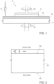
- a CMP apparatus 10 is schematically shown.
- the CMP apparatus 10 comprises, in a per se known way, a polishing head 14, configured to support or carry or hold a wafer 20 (here, of Silicon Carbide, in particular 4H-SiC) during the CMP process.
- a polishing pad 16 is arranged over a supporting platen 17.
- the polishing pad 16 is, for example, of polyurethane.
- the polishing head 14 and the polishing pad 16 faces one another.
- Both the polishing head 14 and the platen 17 are controllable in rotation, as exemplified by arrows 19a, 19b, for performing the CMP process.
- the rotation of the platen 17 causes a corresponding rotation of the polishing pad 16, and the rotation of the polishing head 14 causes a corresponding rotation of the wafer 20.
- a slurry delivery system 18 is also provided, configured to provide a substantially uniform slurry layer (i.e., the chemical-mechanical abrasive) onto the polishing pad 16, in a per se known way.
- a substantially uniform slurry layer i.e., the chemical-mechanical abrasive
- the SiC wafer 20 to be processed has a front side 20a and a back (or bottom) side 20b, opposite to one another.
- the front side 20a has already been processed to manufacture one or more electronic devices, or parts therefor, for example by implanting dopant species, growing or depositing conductive (e.g., of metal material) or insulating layers, etc.
- the back side 20b has been subject to a grinding process, to reduce the thickness of the wafer 20 down to 200 ⁇ m or less.
- the CMP process according to the present description is applied to the bottom side 20b.
- the wafer 20 is of Silicon Carbide (SiC) and has a thickness of, or below, 180 ⁇ m, e.g. between 40 and 180 ⁇ m, and more in particular 100 ⁇ m.
- SiC wafers 20 are manufactured with a thickness of about 350-500 ⁇ m; to achieve the thickness of 180 ⁇ m or less, a grinding step is carried out, as previously discussed.
- the front side 20a of the wafer 20 may be already processed to form, at least in part, electronic components or devices, or any other electrical structure.
- a back side 20b of the wafer 20 is the side processed by the grinding process (and therefore presenting defects/cracks as a consequence of the grinding process), and to be further processed by the CMP process according to the present invention.
- the CMP process according to the present invention is carried out with the following parameters / settings.
- Polishing pad speed and wafer speed are
- Polishing pad speed can affect the entering and leaving of chemical products and reactants between the wafer 20 and the polishing pad 16.
- the wafer speed will affect the speed of the abrasives through the wafer 20.
- the speed of rotation of the polishing pad is set in the range 30-180 rpm, more in particular between 30 and 70 rpm.
- the speed of wafer rotation is defined by the speed of rotation of the support carried 14, and is set in the range 30- 180 rpm, more in particular between 30 and 60 rpm.
- the wafer 20 i.e., the carrier 14
- the polishing pad 16 turn to the same direction of rotation; other embodiments, where the wafer 20 (i.e., the carrier 14) and the polishing pad 16 turn to the opposite direction are possible.
- Pressure is exerted by the polishing head 14 on the polishing pad 16, with the wafer 20 there between.
- the pressure exerted on different areas of the surface 20b of the wafer 20 could, but not necessarily, be different.
- the pressure is set in the range between 5 and 20 kPa.
- Polishing time impact on the material removal rate.
- the selection of polishing time is according to processing quality requirement and / or quantity (thickness) of material to be removed. If polishing time is too long, the abrasives in polishing slurries may lead to secondary injury to the processed surface.
- the thickness of SiC removed at the back side 20b is, in one embodiment, in the range 1-3 ⁇ m; accordingly, polishing time / removal rate are set accordingly to achieve this objective.
- the present Applicant found that removing about 3 ⁇ m of SiC material is enough to remove all defects and cracks at the treated surface (in this example, surface 20b).
- the abrasive slurry is chosen based on its pH property.
- the slurry is chosen with a pH in the range 2-3 (acid).
- the slurry flow rate is, in one possible embodiment, less than 100 ml/min.
- Removal rate can be set freely, for example equal to, or higher than 10 ⁇ m/hr. Lower removal rates (e.g., around 6pm/hr are possible).
- Exemplary slurry include, for example, alumina-based polishing slurries specifically formulated for the chemical mechanical planarization of Silicon Carbide wafers. These slurries, which are known in the art and commercially available, are formulated with permanganate oxidizers, tightly sized engineered nano-particles, and accelerant chemistries that facilitate very low surface finish, defectivity and sub-surface damage on SiC surfaces.
- the CMP process temperature (i.e., temperature of the polishing pad 16) is maintained below 50°C, in particular between ambient temperature (around 24°C) and 50°C.
- wafer warpage at the end of the CMP process is found to be substantially equal to the original wafer warpage, i.e. before the thinning step performed through grinding.
- the appropriate balance between chemical and mechanical factors can reduce the wafer's roughness so as to obtain higher surface shape precision and ensure the desired surface quality.
- the wafer surface 20b after CMP can be inspected through profile testing and its surface roughness can be measured by large area surface profilometer.
- indexes can be measured for the surface quality testing of the wafer. For example, the following parameters have been exemplarily measured: Sa or arithmetical mean height ⁇ 2 nm; Sq or root mean square height ⁇ 10 nm; Sz or maximum height ⁇ 2 nm.
- the invention proposes a way to solve the difficulty to perform a proper stress relief process after SiC wafers grinding ( ⁇ 180 um) due to the high chemical inertness of SiC.
- the proposed solution based on a chemical mechanical surface planarization stress relief process, has demonstrated to be effective on warpage/stress recovery, on surface recovery and mechanical yield.
- the CMP process step can be performed during a device fabrication process flow, after a grinding step, to recover the damages of the grinding step, thus increasing device yield.
- the CMP process described above can be applied on a SiC wafer that is temporarily bonded to a support wafer, which is useful in case of SiC wafer having low thickness, and therefore being fragile and/or difficult to handle.
Landscapes
- Engineering & Computer Science (AREA)
- Mechanical Engineering (AREA)
- Mechanical Treatment Of Semiconductor (AREA)
- Finish Polishing, Edge Sharpening, And Grinding By Specific Grinding Devices (AREA)
- Inorganic Fibers (AREA)
- Carbon And Carbon Compounds (AREA)
Abstract
Description
- The present invention relates to a Chemical Mechanical Polishing, CMP, process applied to a thin wafer of Silicon Carbide, in particular having a thickness of, or lower than, 180µm. The CMP process is aimed at releasing the stress of thinned wafers and recovering surface damages or cracks. The CMP process is carried out at the back side of SiC wafers having a front side already processed (i.e., with electronic components integrated at the front side).
- Integrated circuits are known to be manufactured by alternated steps of deposition and removal of layers belonging to a Silicon and Silicon Carbide wafers; such layers may be either conductive, semiconductive or insulating.
- One manufacturing step involves wafer thinning to guarantee optimal device performances, typically a reduction of the electrical resistance when the device is conducting (Ron resistance). The thinning process is usually performed by mechanical abrasion of a substrate (grinding process).
- On SiC wafers, the grinding process may cause deep sub-surface damage (SSD), with cracks and dislocations, that extends in depth through the Silicon Carbide surface for 1-3 µm.
- Wafer warpage, caused by a compressive stress on the wafer surface, is also a direct consequence of a thinning process by grinding techniques. Stress induced by thinning process and the persistence of cracks increase wafer warpage and makes the dies thus manufactured fragile, impacting mechanical strength and die yield.
- A stress relief step able to recover the original (pre-grinding) wafer surface and hence to recover the wafer warpage to the original, pre-grinding , values, is required to improve Silicon Carbide material quality and consequently the electrical and mechanical quality of the devices integrated therein.
- The present Applicant investigated the use of a thermal process (annealing) to recover the grinding damages; however, this solution is not satisfactory due to thermal constraints that, in some situations (namely, when the wafer has already been processed to manufacture, at least in part, of electronic devices), limit the temperatures below 1000 °C. This thermal budget is not able to guarantee the SiC wafer surface recovery.
- Same considerations can be done for laser annealing that allows local surface heating of the wafer; the thermalinduced stress by laser irradiation is responsible for crystal rearrangement, with new crystal defect and possible cracks creation due to the thermal gradient crated during laser processing between an annealed (thermally stressed) region and a not annealed region.
- Therefore, stress release is a particularly critical step for SiC wafers, having low fracture toughness and extreme brittleness, high hardness and a remarkable chemical inertness. These issues become more serious with SiC substrate having reduced thickness (for example under 180 µm).
- The paper by CHEN GUOMEI et al, "The Effect of Surface Polarity on the CMP Behavior of 6H-SiC Substrates," Russian Journal of Applied Chemistry, vol. 93, no. 6, June 1, 2020, pp. 832-837, XP037195431, discusses the performance of the CMP technique in Silicon and 6H-SiC substrates.
- Document
US2016/133465 describes a method of producing a SiC substrate including a CMP step. - Document
CN105470122 relates to a method of reducing the thickness of a SiC wafer. - However, the above-mentioned problems remain unresolved.
- The aim of the present invention is to provide a CMP process applied to a thin wafer of Silicon Carbide, that overcome the drawbacks mentioned above.
- According to the present invention a CMP process applied to a wafer of Silicon Carbide is provided, as defined in the annexed claims.
- For a better understanding of the invention, some embodiments thereof will now be described, purely by way of non-limiting example and with reference to the attached drawings, wherein:
-
Figure 1 shows a schematic implementation of a CMP apparatus; and -
Figure 2 shows a portion of a wafer during the CMP processing according to the present invention. - In an embodiment of the present invention, a CMP (Chemical-Mechanical_Polishing) process is proposed for overcoming the limitations of the known art.
- With reference to
Figure 1 , aCMP apparatus 10 is schematically shown. - The
CMP apparatus 10 comprises, in a per se known way, apolishing head 14, configured to support or carry or hold a wafer 20 (here, of Silicon Carbide, in particular 4H-SiC) during the CMP process. Apolishing pad 16 is arranged over a supportingplaten 17. Thepolishing pad 16 is, for example, of polyurethane. The polishinghead 14 and thepolishing pad 16 faces one another. - Both the polishing
head 14 and theplaten 17 are controllable in rotation, as exemplified byarrows platen 17 causes a corresponding rotation of thepolishing pad 16, and the rotation of thepolishing head 14 causes a corresponding rotation of thewafer 20. - A
slurry delivery system 18 is also provided, configured to provide a substantially uniform slurry layer (i.e., the chemical-mechanical abrasive) onto thepolishing pad 16, in a per se known way. After-polishing detection and process control equipment, waste treatment and testing equipment, etc., may also be part of theCMP apparatus 10. - The SiC wafer 20 to be processed has a
front side 20a and a back (or bottom)side 20b, opposite to one another. As better discussed in the following, thefront side 20a has already been processed to manufacture one or more electronic devices, or parts therefor, for example by implanting dopant species, growing or depositing conductive (e.g., of metal material) or insulating layers, etc. Theback side 20b has been subject to a grinding process, to reduce the thickness of thewafer 20 down to 200 µm or less. The CMP process according to the present description is applied to thebottom side 20b. - During the CMP process, the
wafer 20, supported/held by thepolishing head 14 at thefront side 20a, is pressed, by thepolishing head 14, against thepolishing pad 16 to process thesurface 20b. In particular, thewafer 20 is of Silicon Carbide (SiC) and has a thickness of, or below, 180µm, e.g. between 40 and 180 µm, and more in particular 100 µm. Usually, SiCwafers 20 are manufactured with a thickness of about 350-500 µm; to achieve the thickness of 180 µm or less, a grinding step is carried out, as previously discussed. - As shown in
Figure 2 , thefront side 20a of thewafer 20 may be already processed to form, at least in part, electronic components or devices, or any other electrical structure. Aback side 20b of thewafer 20 is the side processed by the grinding process (and therefore presenting defects/cracks as a consequence of the grinding process), and to be further processed by the CMP process according to the present invention. - The CMP process according to the present invention is carried out with the following parameters / settings.
- Polishing pad speed can affect the entering and leaving of chemical products and reactants between the
wafer 20 and thepolishing pad 16. The wafer speed will affect the speed of the abrasives through thewafer 20. - The speed of rotation of the polishing pad is set in the range 30-180 rpm, more in particular between 30 and 70 rpm.
- The speed of wafer rotation is defined by the speed of rotation of the support carried 14, and is set in the range 30- 180 rpm, more in particular between 30 and 60 rpm.
- In one embodiment, the wafer 20 (i.e., the carrier 14) and the
polishing pad 16 turn to the same direction of rotation; other embodiments, where the wafer 20 (i.e., the carrier 14) and thepolishing pad 16 turn to the opposite direction are possible. - Pressure is exerted by the
polishing head 14 on thepolishing pad 16, with thewafer 20 there between. - In this process, the pressure exerted on different areas of the
surface 20b of thewafer 20 could, but not necessarily, be different.The pressure is set in the range between 5 and 20 kPa. - Polishing time impact on the material removal rate. The selection of polishing time is according to processing quality requirement and / or quantity (thickness) of material to be removed. If polishing time is too long, the abrasives in polishing slurries may lead to secondary injury to the processed surface.
- The thickness of SiC removed at the
back side 20b is, in one embodiment, in the range 1-3 µm; accordingly, polishing time / removal rate are set accordingly to achieve this objective. - The present Applicant found that removing about 3 µm of SiC material is enough to remove all defects and cracks at the treated surface (in this example,
surface 20b). - The abrasive slurry is chosen based on its pH property. In the present process, the slurry is chosen with a pH in the range 2-3 (acid).
- The slurry flow rate is, in one possible embodiment, less than 100 ml/min.
- Removal rate can be set freely, for example equal to, or higher than 10µm/hr. Lower removal rates (e.g., around 6pm/hr are possible).
- Exemplary slurry include, for example, alumina-based polishing slurries specifically formulated for the chemical mechanical planarization of Silicon Carbide wafers. These slurries, which are known in the art and commercially available, are formulated with permanganate oxidizers, tightly sized engineered nano-particles, and accelerant chemistries that facilitate very low surface finish, defectivity and sub-surface damage on SiC surfaces.
- Other types of slurries can be used.
- The CMP process temperature (i.e., temperature of the polishing pad 16) is maintained below 50°C, in particular between ambient temperature (around 24°C) and 50°C.
- With the above parameters, the Applicant found that the issues of the known art are overcome.
- In particular, cracks and damages at wafer's surface are recovered (eliminated). Furthermore, wafer warpage at the end of the CMP process is found to be substantially equal to the original wafer warpage, i.e. before the thinning step performed through grinding.
- Surface quality is improved with the present CMP process. The appropriate balance between chemical and mechanical factors can reduce the wafer's roughness so as to obtain higher surface shape precision and ensure the desired surface quality. The
wafer surface 20b after CMP can be inspected through profile testing and its surface roughness can be measured by large area surface profilometer. For the surface quality testing of the wafer, several indexes can be measured. For example, the following parameters have been exemplarily measured: Sa or arithmetical mean height < 2 nm; Sq or root mean square height < 10 nm; Sz or maximum height < 2 nm. - The advantages achieved by the present invention are apparent from the above description.
- The invention proposes a way to solve the difficulty to perform a proper stress relief process after SiC wafers grinding (<180 um) due to the high chemical inertness of SiC. The proposed solution, based on a chemical mechanical surface planarization stress relief process, has demonstrated to be effective on warpage/stress recovery, on surface recovery and mechanical yield. The CMP process step can be performed during a device fabrication process flow, after a grinding step, to recover the damages of the grinding step, thus increasing device yield.
- Finally, it is evident that modifications and variations may be made to the present disclosure, without departing from the scope of the invention, as defined in the annexed claims.
- For example, the CMP process described above can be applied on a SiC wafer that is temporarily bonded to a support wafer, which is useful in case of SiC wafer having low thickness, and therefore being fragile and/or difficult to handle.
Claims (7)
- A Chemical Mechanical Polishing, CMP, process applied to a wafer (20) of Silicon Carbide having a thickness of, or lower than, 180pm, comprising the steps of:- arranging the wafer (20) on a supporting head (14) of a CMP processing apparatus (10), the wafer (20) having a front side (20a) and a back side (20b) opposite to one another, wherein at least one electronic component is present at the front side (20a), and wherein the front side (20a) is coupled to the supporting head (14);- deliver a polishing slurry on the wafer (20), wherein the polishing slurry has a pH in the range 2-3;- pressing the back side (20b) of the wafer (20) against a polishing pad (16) of the CMP apparatus (10) exerting, by the supporting head (14), a pressure on the polishing pad (16) in the range 5-20 kPa;- setting a rotation of the polishing pad (16) in the range 30-180 rpm, and setting a rotation of polishing head (14) in the range 30-180 rpm;- setting and maintaining a CMP process temperature equal to, or below, 50°C.
- The CMP process of claim 1, wherein the flow rate of the polishing slurry is less than 100 ml/min.
- The CMP process of claim 1 or claim 2, wherein the polishing slurry is alumina-based.
- The CMP process of anyone of the preceding claims, wherein the CMP process is executed until a thickness between 1 and 3 µm of material is removed from the back side (20b) of the wafer (20).
- The CMP process of anyone of the preceding claims, wherein the direction of rotation of the polishing pad (16) is the same to the rotation of the supporting head (14).
- The CMP process of anyone of the preceding claims, wherein the rotation of the polishing pad (16) is set in the range 30-70 rpm, and the rotation of polishing head (14) is set in the range 30-60 rpm.
- The CMP process of anyone of the preceding claims, wherein the wafer (20) is of 4H-Silicon Carbide, 4H-SiC.
Applications Claiming Priority (1)
| Application Number | Priority Date | Filing Date | Title |
|---|---|---|---|
| IT102021000027467A IT202100027467A1 (en) | 2021-10-26 | 2021-10-26 | CMP PROCESS APPLIED TO A THIN SIC SLICE FOR STRESS RELEASE AND DAMAGE RECOVERY |
Publications (1)
| Publication Number | Publication Date |
|---|---|
| EP4174915A1 true EP4174915A1 (en) | 2023-05-03 |
Family
ID=79164573
Family Applications (1)
| Application Number | Title | Priority Date | Filing Date |
|---|---|---|---|
| EP22198683.9A Pending EP4174915A1 (en) | 2021-10-26 | 2022-09-29 | Cmp process applied to a thin sic wafer for stress release and damage recovery |
Country Status (5)
| Country | Link |
|---|---|
| US (1) | US20230128739A1 (en) |
| EP (1) | EP4174915A1 (en) |
| JP (1) | JP2023064715A (en) |
| CN (1) | CN116021417A (en) |
| IT (1) | IT202100027467A1 (en) |
Families Citing this family (2)
| Publication number | Priority date | Publication date | Assignee | Title |
|---|---|---|---|---|
| US12610767B2 (en) * | 2024-03-07 | 2026-04-21 | Wolfspeed, Inc. | Additives for grinding semiconductor workpieces |
| CN120206314B (en) * | 2025-05-09 | 2025-09-05 | 河北同光半导体股份有限公司 | Chemical mechanical polishing method for large-size silicon carbide substrate |
Citations (2)
| Publication number | Priority date | Publication date | Assignee | Title |
|---|---|---|---|---|
| CN105470122A (en) | 2015-11-20 | 2016-04-06 | 成都嘉石科技有限公司 | SiC thinning method |
| US20160133465A1 (en) | 2013-06-24 | 2016-05-12 | Showa Denko K.K. | METHOD FOR PRODUCING SiC SUBSTRATE |
Family Cites Families (6)
| Publication number | Priority date | Publication date | Assignee | Title |
|---|---|---|---|---|
| US5597442A (en) * | 1995-10-16 | 1997-01-28 | Taiwan Semiconductor Manufacturing Company Ltd. | Chemical/mechanical planarization (CMP) endpoint method using measurement of polishing pad temperature |
| CN101007396A (en) * | 2006-01-24 | 2007-08-01 | 联华电子股份有限公司 | Polishing head applied to chemical mechanical polishing process and chemical mechanical polishing method |
| US8568610B2 (en) * | 2010-09-20 | 2013-10-29 | Rohm And Haas Electronic Materials Cmp Holdings, Inc. | Stabilized, concentratable chemical mechanical polishing composition and method of polishing a substrate |
| CN101966689B (en) * | 2010-09-27 | 2013-04-10 | 山东大学 | Surface polishing method for carbon surface of large-diameter 4H-SiC wafer |
| US10030319B2 (en) * | 2014-11-27 | 2018-07-24 | Sumitomo Electric Industries, Ltd. | Silicon carbide substrate, method for producing same, and method for manufacturing silicon carbide semiconductor device |
| CN111745468A (en) * | 2020-06-04 | 2020-10-09 | 东莞市天域半导体科技有限公司 | Method for quickly polishing silicon carbide wafer by adopting diamond polishing paste |
-
2021
- 2021-10-26 IT IT102021000027467A patent/IT202100027467A1/en unknown
-
2022
- 2022-09-29 EP EP22198683.9A patent/EP4174915A1/en active Pending
- 2022-10-07 US US17/962,090 patent/US20230128739A1/en active Pending
- 2022-10-18 JP JP2022166993A patent/JP2023064715A/en active Pending
- 2022-10-25 CN CN202211312232.1A patent/CN116021417A/en active Pending
Patent Citations (2)
| Publication number | Priority date | Publication date | Assignee | Title |
|---|---|---|---|---|
| US20160133465A1 (en) | 2013-06-24 | 2016-05-12 | Showa Denko K.K. | METHOD FOR PRODUCING SiC SUBSTRATE |
| CN105470122A (en) | 2015-11-20 | 2016-04-06 | 成都嘉石科技有限公司 | SiC thinning method |
Non-Patent Citations (3)
| Title |
|---|
| CHEN GUOMEI ET AL.: "The Effect of Surface Polarity on the CMP Behavior of 6H-SiC Substrates", RUSSIAN JOURNAL OF APPLIED CHEMISTRY, vol. 93, 1 June 2020 (2020-06-01), pages 832 - 837, XP037195431, DOI: 10.1134/S1070427220060099 |
| CHEN GUOMEI ET AL: "The Effect of Surface Polarity on the CMP Behavior of 6H-SiC Substrates", RUSSIAN JOURNAL OF APPLIED CHEMISTRY, PLEIADES PUBLISHING, MOSCOW, vol. 93, no. 6, 1 June 2020 (2020-06-01), pages 832 - 837, XP037195431, ISSN: 1070-4272, DOI: 10.1134/S1070427220060099 * |
| TAO YIN ET AL: "The Effects of Strong Oxidizing Slurry and Processing Atmosphere on Double-sided CMP of SiC Wafer", vol. 591-593, no. Part 2, 1 January 2012 (2012-01-01), pages 1131 - 1134, XP009542591, ISSN: 1022-6680, Retrieved from the Internet <URL:https://www.scientific.net/AMR.591-593.1131> [retrieved on 20121101], DOI: 10.4028/WWW.SCIENTIFIC.NET/AMR.591-593.1131 * |
Also Published As
| Publication number | Publication date |
|---|---|
| US20230128739A1 (en) | 2023-04-27 |
| CN116021417A (en) | 2023-04-28 |
| JP2023064715A (en) | 2023-05-11 |
| IT202100027467A1 (en) | 2023-04-26 |
Similar Documents
| Publication | Publication Date | Title |
|---|---|---|
| EP1189266B1 (en) | Production method for silicon wafer and soi wafer, and soi wafer | |
| US9396945B2 (en) | Method for producing SiC substrate | |
| TW201724177A (en) | Method for manufacturing SiC composite substrate and method for manufacturing semiconductor substrate | |
| US20230128739A1 (en) | Cmp process applied to a thin sic wafer for stress release and damage recovery | |
| JP5014737B2 (en) | Method for manufacturing SiC single crystal substrate | |
| KR101752986B1 (en) | METHOD FOR PRODUCING SiC SUBSTRATE | |
| CN102668043A (en) | Semiconductor wafer re-use using chemical mechanical polishing | |
| CN107615445B (en) | Manufacturing method of silicon-on-insulator wafer | |
| JP3904943B2 (en) | Sapphire wafer processing method and electronic device manufacturing method | |
| KR20240141304A (en) | Manufacturing process of non-deformable p-SiC wafers | |
| JP2004131328A (en) | Method for manufacturing silicon carbide single crystal wafer, and silicon carbide single crystal wafer | |
| US7060620B2 (en) | Method of preparing a surface of a semiconductor wafer to make it epiready | |
| CN112585724B (en) | Manufacturing method of SiC chip | |
| CN114730699A (en) | Method for producing a composite structure comprising a thin layer of single crystal SiC on a carrier substrate made of SiC | |
| US20260090307A1 (en) | Method for thinning a composite structure carried by a polycrystalline sic carrier substrate, with reduced warpage | |
| CN110140195B (en) | Method for polishing silicon wafer, method for manufacturing silicon wafer, and silicon wafer | |
| CN114250516B (en) | Silicon carbide wafer, method for manufacturing the same, and semiconductor device | |
| JP2014213403A (en) | Method for reducing warpage of substrate, method for manufacturing substrate, and sapphire substrate | |
| JP2000077372A (en) | Method for manufacturing semiconductor wafer for vapor phase growth | |
| JP2007284283A (en) | GaN single crystal substrate processing method and GaN single crystal substrate | |
| JP4655861B2 (en) | Manufacturing method of substrate for electronic device | |
| JP2004063617A (en) | Jig for heat treating silicon wafer | |
| CN102725838B (en) | Method for processing temporarily bonded product wafers | |
| EP4670910A1 (en) | METHOD FOR GRINDING A SEMICONDUCTOR CRYSTAL AND METHOD FOR PRODUCING AN ENHANCED SIC BLOCK USING THIS GRINDING METHOD | |
| CN118048691A (en) | Method for manufacturing laminated wafer and laminated wafer |
Legal Events
| Date | Code | Title | Description |
|---|---|---|---|
| PUAI | Public reference made under article 153(3) epc to a published international application that has entered the european phase |
Free format text: ORIGINAL CODE: 0009012 |
|
| STAA | Information on the status of an ep patent application or granted ep patent |
Free format text: STATUS: THE APPLICATION HAS BEEN PUBLISHED |
|
| STAA | Information on the status of an ep patent application or granted ep patent |
Free format text: STATUS: REQUEST FOR EXAMINATION WAS MADE |
|
| AK | Designated contracting states |
Kind code of ref document: A1 Designated state(s): AL AT BE BG CH CY CZ DE DK EE ES FI FR GB GR HR HU IE IS IT LI LT LU LV MC MK MT NL NO PL PT RO RS SE SI SK SM TR |
|
| 17P | Request for examination filed |
Effective date: 20230424 |
|
| RBV | Designated contracting states (corrected) |
Designated state(s): AL AT BE BG CH CY CZ DE DK EE ES FI FR GB GR HR HU IE IS IT LI LT LU LV MC MK MT NL NO PL PT RO RS SE SI SK SM TR |
|
| STAA | Information on the status of an ep patent application or granted ep patent |
Free format text: STATUS: EXAMINATION IS IN PROGRESS |
|
| 17Q | First examination report despatched |
Effective date: 20250124 |