EP4174561A1 - Electro-absorption modulator - Google Patents
Electro-absorption modulator Download PDFInfo
- Publication number
- EP4174561A1 EP4174561A1 EP22203638.6A EP22203638A EP4174561A1 EP 4174561 A1 EP4174561 A1 EP 4174561A1 EP 22203638 A EP22203638 A EP 22203638A EP 4174561 A1 EP4174561 A1 EP 4174561A1
- Authority
- EP
- European Patent Office
- Prior art keywords
- eam
- material layer
- quantum well
- graded
- range
- Prior art date
- Legal status (The legal status is an assumption and is not a legal conclusion. Google has not performed a legal analysis and makes no representation as to the accuracy of the status listed.)
- Granted
Links
Images



Classifications
-
- G—PHYSICS
- G02—OPTICS
- G02F—OPTICAL DEVICES OR ARRANGEMENTS FOR THE CONTROL OF LIGHT BY MODIFICATION OF THE OPTICAL PROPERTIES OF THE MEDIA OF THE ELEMENTS INVOLVED THEREIN; NON-LINEAR OPTICS; FREQUENCY-CHANGING OF LIGHT; OPTICAL LOGIC ELEMENTS; OPTICAL ANALOGUE/DIGITAL CONVERTERS
- G02F1/00—Devices or arrangements for the control of the intensity, colour, phase, polarisation or direction of light arriving from an independent light source, e.g. switching, gating or modulating; Non-linear optics
- G02F1/01—Devices or arrangements for the control of the intensity, colour, phase, polarisation or direction of light arriving from an independent light source, e.g. switching, gating or modulating; Non-linear optics for the control of the intensity, phase, polarisation or colour
- G02F1/015—Devices or arrangements for the control of the intensity, colour, phase, polarisation or direction of light arriving from an independent light source, e.g. switching, gating or modulating; Non-linear optics for the control of the intensity, phase, polarisation or colour based on semiconductor elements having potential barriers, e.g. having a PN or PIN junction
- G02F1/0155—Devices or arrangements for the control of the intensity, colour, phase, polarisation or direction of light arriving from an independent light source, e.g. switching, gating or modulating; Non-linear optics for the control of the intensity, phase, polarisation or colour based on semiconductor elements having potential barriers, e.g. having a PN or PIN junction modulating the optical absorption
- G02F1/0157—Devices or arrangements for the control of the intensity, colour, phase, polarisation or direction of light arriving from an independent light source, e.g. switching, gating or modulating; Non-linear optics for the control of the intensity, phase, polarisation or colour based on semiconductor elements having potential barriers, e.g. having a PN or PIN junction modulating the optical absorption using electro-absorption effects, e.g. Franz-Keldysh [FK] effect or quantum confined stark effect [QCSE]
-
- G—PHYSICS
- G02—OPTICS
- G02F—OPTICAL DEVICES OR ARRANGEMENTS FOR THE CONTROL OF LIGHT BY MODIFICATION OF THE OPTICAL PROPERTIES OF THE MEDIA OF THE ELEMENTS INVOLVED THEREIN; NON-LINEAR OPTICS; FREQUENCY-CHANGING OF LIGHT; OPTICAL LOGIC ELEMENTS; OPTICAL ANALOGUE/DIGITAL CONVERTERS
- G02F1/00—Devices or arrangements for the control of the intensity, colour, phase, polarisation or direction of light arriving from an independent light source, e.g. switching, gating or modulating; Non-linear optics
- G02F1/01—Devices or arrangements for the control of the intensity, colour, phase, polarisation or direction of light arriving from an independent light source, e.g. switching, gating or modulating; Non-linear optics for the control of the intensity, phase, polarisation or colour
- G02F1/015—Devices or arrangements for the control of the intensity, colour, phase, polarisation or direction of light arriving from an independent light source, e.g. switching, gating or modulating; Non-linear optics for the control of the intensity, phase, polarisation or colour based on semiconductor elements having potential barriers, e.g. having a PN or PIN junction
- G02F1/017—Structures with periodic or quasi periodic potential variation, e.g. superlattices, quantum wells
- G02F1/01725—Non-rectangular quantum well structures, e.g. graded or stepped quantum wells
Definitions
- the present invention concerns electro-absorption modulators (EAMs).
- EAMs electro-absorption modulators
- this invention concerns EAMs comprising one or more quantum well structures.
- the invention also concerns a modulating retroreflector (MRR) comprising the inventive EAM.
- MRR modulating retroreflector
- the invention also concerns a free-space optical communications system, comprising the inventive MRR
- Electro-absorption modulators have applications in many optoelectronic systems, including, but not limited to, photonic integrated circuits, fiber optics, and free space optical communication.
- EAMs are often used to alter the intensity of light over time, embedding highs and lows ("Is” and “0s”, or “ons” and “offs”) into a continuous beam to transmit binary data. This is done by changing the absorption of the material by applying a voltage across it thereby setting up an electric field within it, creating (for the same wavelength) a regime of low absorption and a regime of high absorption.
- SWaP weight and power
- Rectangular quantum wells are currently used to increase the strength of the modulation effects in EAMs operating at higher temperatures. Multiple such rectangular quantum wells may be employed in series, resulting in a so-called multiple quantum well (MQW) device.
- MQW multiple quantum well
- Such EAMs based on quantum wells utilize the quantum confined Stark effect (QCSE).
- the present invention seeks to provide improved EAMs utilising novel quantum well structures, with applications such as, but not limited to, enhanced modulating retroreflectors (MRRs).
- MRRs enhanced modulating retroreflectors
- the present invention provides, according to a first aspect, an electro-absorption modulator, EAM, comprising a quantum well configured to provide a variable electromagnetic absorption spectrum in response to an applied electric field.
- the quantum well is a type-II quantum well comprising two material layers. Each material layer has a graded material composition, such that the potential in each material layer varies as a function of position.
- graded material composition it is meant that the material composition of the layer varies over the layer, i.e. the relative proportions of different elements forming the layer change throughout the layer. This results in a non-rectangular potential in the quantum well, such that the potential in the well varies as a function of position, rather than being constant, as in the case of a rectangular quantum well, for example.
- the performance of an EAM having one or more such quantum wells can be improved, in terms of reduced insertion loss and enhanced extinction ratio, for example. This arises as a result of the manner in which the electron, heavy-hole and light-hole wave functions are transformed by the varying, non-rectangular potential.
- the potential in the quantum well may be parabolic as a function of position.
- the potential in the quantum well may be triangular as a function of position.
- the quantum well may comprise a first material layer of AlInAs directly adjacent to a second material layer of InAsP.
- the first material layer of AlInAs may have a thickness in the range 15 nm to 25 nm.
- the second material layer of InAsP may have a thickness in the range 10 nm to 20 nm.
- the proportion of Al may be graded in the range 0.5 to 0.3.
- the proportion of As may be graded in the range 0.4 to 0.2.
- the quantum well may comprise a first material layer of InGaAs directly adjacent to a second material layer of GaAsSb.
- the first material layer of InGaAs may have a thickness in the range 15 nm to 25 nm.
- the second material layer of GaAsSb may have a thickness in the range 10 nm to 20 nm.
- the proportion of In may be graded in the range 0.35 to 0.55.
- the proportion of As may be graded in the range 0.4 to 0.6.
- the EAM may comprise a quantum well region comprising multiple said type-II quantum wells arranged adjacent to each other to provide a multiple quantum well, MQW, structure.
- MQW multiple quantum well
- a modulating retroreflector comprising the EAM of the first aspect.
- MRR modulating retroreflector
- a free-space optical communications system comprising the MRR of the second aspect.
- the MRR may be located on a mobile platform, such as an unmanned aerial vehicle.
- FIG. 1 shows an electro-absorption modulator (EAM) 100 according to embodiments of the invention.
- the EAM comprises one or more quantum wells 102 within some substrate material 104.
- a voltage V can be applied across the EAM in order to establish an electric field within the one or more quantum wells 102 of the EAM.
- This has the effect of changing the electro-magnetic absorption spectrum of the EAM as a result of the quantum confined Stark effect.
- an incoming beam of electromagnetic radiation 106 for example near infrared light, can be intensity modulated by modulating the applied voltage V. This effect can be used to produce an on-off keyed output beam 108 and therefore to encode data for onward transmission.
- Figure 2 shows example absorption spectra at different applied voltages for a conventional EAM having one or more rectangular quantum wells.
- the absorption coefficient of the EAM can be varied as a function of applied voltage sufficiently to produce an on-off keyed output optical signal.
- Quantum wells can be categorised as being either of type-I or type-II.
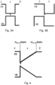
- Figure 3A illustrates the energy band structure of a type-I rectangular quantum well
- Figure 3B illustrates the energy band structure of a type-II rectangular quantum well.
- absorption occurs only in material 1 having the smaller band gap (as illustrated by the arrow between the valence and conduction bands of material 1)
- absorption occurs between materials 1 and 2 (as illustrated by the arrow between the valence band of material 2 and the conduction band of material 1).
- Figure 4 shows schematically the conduction and valence band configuration of a type-I quantum well having a graded material composition.
- the quantum well comprises a material layer, labelled "1", having a graded material composition, such that the potential in the quantum well varies as a function of position.
- graded material composition it should be understood that the material composition changes over the layer.
- the composition of the layer is graded through a range of material compositions, such as In (0.35-0.47) Ga (0.65-0.53) As.
- the material composition of the layer is graded linearly, giving rise to a potential which is triangular in shape, i.e. it varies linearly over the layer.
- a potential which is triangular in shape
- more complex structures, such as parabolic potentials can be created by grading the material composition of the graded layer accordingly.
- the shape of the potential created by grading the material composition can be either symmetric or asymmetric.
- Figure 4 shows an asymmetric triangular potential in a type-I quantum well
- Figure 5 shows an example of a symmetric triangular potential in a type-I quantum well.
- Figures 4 and 5 are not embodiments of the invention as they relate to type-I quantum wells.
- layers of a type-II quantum well can be graded in a corresponding manner.
- Figure 6 shows the conduction and valence band configuration of a type-II quantum well employed within an EAM according to an embodiment of the invention.
- the type-II quantum well comprises two material layers, labelled "1A" and "1B" each of which has a graded material composition.
- the layers labelled “2" may be described as the barrier material. This is a semiconductor of larger bandgap than the materials used in the quantum well layers, and these provide a barrier to adjacent wells (if present), to prevent coupling of the wave functions between adjacent wells.
- This barrier layer material is not graded, i.e. it contains a single material composition.
- Figure 6 shows a single period of a graded type-II quantum well.
- a multiple quantum well structure would contain two or more repetitions or periods of this singular quantum well, each separated by such barrier layers.
- the material composition in the quantum well is graded in such a manner as to give an asymmetric triangular potential.
- absorption takes place across adjacent layers.
- the graded potential maintains proximity between the wavefunctions, which has been found to enhance electro-absorption.
- the inventors have appreciated that the shape of the potential, and whether the potential is made symmetric or asymmetric, all provide varying control over the optical and electrical properties of the quantum well and hence of the EAM in which one or more of the quantum wells are employed.
- EAMs according to embodiments of the invention provide enhanced performance in terms of one or more of the modulation speed, insertion loss, and extinction ratio.
- the insertion loss (IL) is defined as the loss of optical power from transmission through a component, in the case of the electro-absorption modulator, this is when operated for lowest absorption (in "on" state).
- IL insertion loss
- this is directly proportional to the overlap between wavefunctions in the conduction and valence bands.
- the wavefunction overlap integral gives a value between 0 and 1, referring to 0% and 100% of potential material absorption respectively.
- type-I quantum wells this value is often around 1, due to the straddling band alignment and absorption taking place in the same material layer, resulting in high IL.
- the inventors have appreciated that type-II graded quantum wells significantly reduce the wavefunction overlap integral, due to spatial separation across adjacent layers.
- the extinction ratio is defined as the ratio between the power transmitted by the component when operated for minimum absorption ("on” state) and the power transmitted by the component when operated for maximum absorption ("off” state). In quantum wells, this can be manifested as the change in the wavefunction overlap integral when an external electric field is applied.
- the inventors have appreciated that significant benefits are observed in type-II graded quantum wells due to the ability to tailor the separation of the wavefunctions such that they do not overlap at zero applied field but are so close that a small applied voltage increases the overlap significantly. Accordingly, a greater increase in overlap at lower electric fields is achieved, resulting in enhanced ERs.
- the modulation speed of a quantum well electro-absorption modulator is dictated by a time constant proportional to the capacitance of the device.
- the switching capabilities of said devices are directly proportional to area, which can be aided through reductions in pixel size, and are inversely proportional to the total thickness of the intrinsic part of the device.
- type-II graded quantum wells increased overall thickness with reduced IL and increased ER allows for significantly increased modulation speed for the equal IL and ER in equivalent rectangular quantum well structures.
- type-II graded quantum wells yield reductions in power consumption, requiring lower voltages to impart the same modulation. Furthermore, due to spatial separation of the wavefunctions, the low absorption regime occurs when the device receives no voltage, giving an "on" signal through the device, which is energetically favourable for modulator operation, resulting in a lower average power requirement.
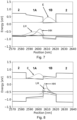
- Figure 7 shows the simulated band structure of a quantum well according to embodiments of the invention, having a 19 nm thick Al (0.47-0.38) InAs layer adjacent to a 16 nm thick InAs (0.35-0.25) P layer, on an InP substrate.
- Figure 8 shows the simulated band structure of a quantum well according to embodiments of the invention, having 20 nm thick In (0.35-0.55) GaAs layer adjacent to a 15nm thick GaAs (0.4-0.6) Sb layer on a GaAs substrate.
- the simulated electron (E), heavy-hole (HH) and light-hole (LH) wavefunctions are also illustrated for both cases, in which the minimal overlap between the electron and hole wavefunctions is apparent.
- the inventors have observed significant reductions in the predicted IL and substantial increases in the ER. It should be appreciated that the overall magnitude of the IL is dependent on the number of quantum wells in the EAM, and this will vary depending on the application. However, for comparison, a conventional structure has a ⁇ well , which denotes the fraction of light absorbed by each quantum well, of 0.0005 and an extinction ratio of 2dB. To compare different quantum wells, a figure of merit may be defined as the ratio between the extinction ratio and the insertion loss. The model results predict ⁇ well values over an order of magnitude lower than conventional quantum wells and an extinction ratio of almost double that of conventional quantum wells.
- Figure 9 shows simulated ⁇ well values for the quantum well structures of Figures 7 and 8 .
- Figure 10 shows simulated extinction ratio values for the quantum well structures of Figures 7 and 8 .
- Quantum well structures of the kind shown in Figures 7 and 8 can be layered in series to provide a multiple quantum well MQW structure with applications in enhanced EAMs.
- Such enhanced EAMs have a breadth of applications in low-loss, high performance optoelectronic systems.
- EAMs are typically operated in either normal incidence or edge incidence. Normal incidence devices typically require significant numbers of quantum wells to be grown to achieve reasonable performance. This is due to a relatively small interaction length between the light and the quantum wells.
- Edge-incident devices can make use of very long interactions lengths and require significantly fewer quantum wells.
- GaAs and InP based heterostructures are of interest.
- compounds of interest for the quantum wells include InGaAs-GaAsSb as well as InAsP-InGaAs-InP, GaAsSb-InGaAsN-GaAs, InGaAs-GaAsSbBi-GaAs, InAlAs-InPSb-InP, and InGaAsP with either GaAs or InP for 1310nm or 1550nm operation respectively.
- MRR 200 modulating retroreflector
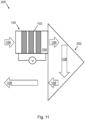
- An MRR 200 according to embodiments of the invention is illustrated schematically in Figure 11 .
- the MRR 200 combines an EAM 100 as herein described, having a type-II quantum well which comprises two material layers having graded material compositions, with a corner cube retroreflector 202. Accordingly, an incident beam of light 106 can be intensity modulated by modulating the voltage V applied to the EAM and the modulated beam of light 108 is returned to the source by virtue of the retroreflector.
- Such an MRR 200 is anticipated to have utility in free space optical communication in aerospace applications.
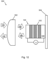
- FIG 12 illustrates an alternative MRR 300 according to embodiments of the invention.
- the MRR 300 combines an EAM 100 as herein described with a retroreflector.
- the retroreflector is in the form of a so-called cats-eye retroreflector. This uses a lens 302 (or a combination of lenses) which direct light to the EAM 100 which is backed by a mirror 304.
Landscapes
- Physics & Mathematics (AREA)
- Nonlinear Science (AREA)
- General Physics & Mathematics (AREA)
- Optics & Photonics (AREA)
- Optical Modulation, Optical Deflection, Nonlinear Optics, Optical Demodulation, Optical Logic Elements (AREA)
- Recrystallisation Techniques (AREA)
Abstract
Description
- The present invention concerns electro-absorption modulators (EAMs).
- More particularly, but not exclusively, this invention concerns EAMs comprising one or more quantum well structures.
- The invention also concerns a modulating retroreflector (MRR) comprising the inventive EAM.
- The invention also concerns a free-space optical communications system, comprising the inventive MRR
- Electro-absorption modulators (EAMs) have applications in many optoelectronic systems, including, but not limited to, photonic integrated circuits, fiber optics, and free space optical communication.
- EAMs are often used to alter the intensity of light over time, embedding highs and lows ("Is" and "0s", or "ons" and "offs") into a continuous beam to transmit binary data. This is done by changing the absorption of the material by applying a voltage across it thereby setting up an electric field within it, creating (for the same wavelength) a regime of low absorption and a regime of high absorption.
- This can be used as a compact, lightweight, and low power consuming method of embedding data into an optical signal, which has implications on miniaturizing technology with increasing size, weight and power (SWaP) restrictions.
- Rectangular quantum wells (narrow planar layers) are currently used to increase the strength of the modulation effects in EAMs operating at higher temperatures. Multiple such rectangular quantum wells may be employed in series, resulting in a so-called multiple quantum well (MQW) device. Such EAMs based on quantum wells utilize the quantum confined Stark effect (QCSE).
- The present invention seeks to provide improved EAMs utilising novel quantum well structures, with applications such as, but not limited to, enhanced modulating retroreflectors (MRRs).
- The present invention provides, according to a first aspect, an electro-absorption modulator, EAM, comprising a quantum well configured to provide a variable electromagnetic absorption spectrum in response to an applied electric field. The quantum well is a type-II quantum well comprising two material layers. Each material layer has a graded material composition, such that the potential in each material layer varies as a function of position.
- By graded material composition, it is meant that the material composition of the layer varies over the layer, i.e. the relative proportions of different elements forming the layer change throughout the layer. This results in a non-rectangular potential in the quantum well, such that the potential in the well varies as a function of position, rather than being constant, as in the case of a rectangular quantum well, for example. In this manner, the performance of an EAM having one or more such quantum wells can be improved, in terms of reduced insertion loss and enhanced extinction ratio, for example. This arises as a result of the manner in which the electron, heavy-hole and light-hole wave functions are transformed by the varying, non-rectangular potential.
- The potential in the quantum well may be parabolic as a function of position. Alternatively, the potential in the quantum well may be triangular as a function of position.
- The quantum well may comprise a first material layer of AlInAs directly adjacent to a second material layer of InAsP. The first material layer of AlInAs may have a thickness in the range 15 nm to 25 nm. The second material layer of InAsP may have a thickness in the range 10 nm to 20 nm. In the first material layer, the proportion of Al may be graded in the range 0.5 to 0.3. In the second material layer, the proportion of As may be graded in the range 0.4 to 0.2.
- The quantum well may comprise a first material layer of InGaAs directly adjacent to a second material layer of GaAsSb. The first material layer of InGaAs may have a thickness in the range 15 nm to 25 nm. The second material layer of GaAsSb may have a thickness in the range 10 nm to 20 nm. In the first material layer, the proportion of In may be graded in the range 0.35 to 0.55. In the second material layer, the proportion of As may be graded in the range 0.4 to 0.6.
- The EAM may comprise a quantum well region comprising multiple said type-II quantum wells arranged adjacent to each other to provide a multiple quantum well, MQW, structure. Such an MQW structure is anticipated to provide improved performance compared to an EAM employing only a single quantum well.
- According to a second aspect of the invention, there is also provided a modulating retroreflector, MRR, comprising the EAM of the first aspect. Such an MRR will benefit from the improved performance of the constituent EAM and provide improved utility in free-space optical communication applications.
- According to a third aspect of the invention, there is also provided a free-space optical communications system, comprising the MRR of the second aspect. In such a free-space optical communications system, the MRR may be located on a mobile platform, such as an unmanned aerial vehicle.
- It will of course be appreciated that features described in relation to one aspect of the present invention may be incorporated into other aspects of the present invention.
- Embodiments of the present invention will now be described by way of example only with reference to the accompanying schematic drawings of which:
-
Figure 1 shows a schematic view of an electro-absorption modulator according to embodiments of the invention. -
Figure 2 shows example absorption spectra at different applied voltages for a conventional EAM having one or more rectangular quantum wells. -
Figure 3A shows the energy band structure of a type-I rectangular quantum well. -
Figure 3B shows the energy band structure of a type-II rectangular quantum well. -
Figures 4 and5 show the conduction and valence band configuration of type-I quantum wells having a graded material composition. -
Figure 6 shows the conduction and valence band configuration of a type-II quantum well employed within EAMs according to embodiments of the invention and having a graded material composition in two layers. -
Figures 7 and 8 show simulated band structures of type-II quantum wells used in EAMs according to embodiments of the invention. -
Figures 9 and 10 show simulated optical characteristics of the type-II quantum wells shown inFigures 7 and 8 respectively. -
Figure 11 shows a schematic view of a modulating retroreflector having an EAM according to embodiments of the invention. -
Figure 12 shows a schematic view of an alternative modulating retroreflector having an EAM according to embodiments of the invention. -
Figure 1 shows an electro-absorption modulator (EAM) 100 according to embodiments of the invention. The EAM comprises one or morequantum wells 102 within somesubstrate material 104. A voltage V can be applied across the EAM in order to establish an electric field within the one or morequantum wells 102 of the EAM. This has the effect of changing the electro-magnetic absorption spectrum of the EAM as a result of the quantum confined Stark effect. Accordingly, an incoming beam ofelectromagnetic radiation 106, for example near infrared light, can be intensity modulated by modulating the applied voltage V. This effect can be used to produce an on-offkeyed output beam 108 and therefore to encode data for onward transmission. -
Figure 2 shows example absorption spectra at different applied voltages for a conventional EAM having one or more rectangular quantum wells. At the operating wavelength, the absorption coefficient of the EAM can be varied as a function of applied voltage sufficiently to produce an on-off keyed output optical signal. - Quantum wells can be categorised as being either of type-I or type-II.
Figure 3A illustrates the energy band structure of a type-I rectangular quantum well, whereasFigure 3B illustrates the energy band structure of a type-II rectangular quantum well. In the type-I quantum well, absorption occurs only inmaterial 1 having the smaller band gap (as illustrated by the arrow between the valence and conduction bands of material 1), whereas in the type-II quantum well, absorption occurs betweenmaterials 1 and 2 (as illustrated by the arrow between the valence band ofmaterial 2 and the conduction band of material 1). - In contrast to the rectangular quantum wells of
Figures 3A and 3B, Figure 4 shows schematically the conduction and valence band configuration of a type-I quantum well having a graded material composition. The quantum well comprises a material layer, labelled "1", having a graded material composition, such that the potential in the quantum well varies as a function of position. By graded material composition, it should be understood that the material composition changes over the layer. As an example, rather than growing a single 100 nm thick layer of In(0.43)Ga(0.57)As (43% InAs and 57% GaAs), the composition of the layer is graded through a range of material compositions, such as In(0.35-0.47)Ga(0.65-0.53)As. - In
Figure 4 , the material composition of the layer is graded linearly, giving rise to a potential which is triangular in shape, i.e. it varies linearly over the layer. However, it should be appreciated that more complex structures, such as parabolic potentials can be created by grading the material composition of the graded layer accordingly. It should also be appreciated that the shape of the potential created by grading the material composition can be either symmetric or asymmetric.Figure 4 shows an asymmetric triangular potential in a type-I quantum well, whereasFigure 5 shows an example of a symmetric triangular potential in a type-I quantum well.Figures 4 and5 are not embodiments of the invention as they relate to type-I quantum wells. However, it should be appreciated that layers of a type-II quantum well can be graded in a corresponding manner. -
Figure 6 shows the conduction and valence band configuration of a type-II quantum well employed within an EAM according to an embodiment of the invention. The type-II quantum well comprises two material layers, labelled "1A" and "1B" each of which has a graded material composition. The layers labelled "2" may be described as the barrier material. This is a semiconductor of larger bandgap than the materials used in the quantum well layers, and these provide a barrier to adjacent wells (if present), to prevent coupling of the wave functions between adjacent wells. This barrier layer material is not graded, i.e. it contains a single material composition. -
Figure 6 shows a single period of a graded type-II quantum well. A multiple quantum well structure would contain two or more repetitions or periods of this singular quantum well, each separated by such barrier layers. - In the embodiment of
Figure 6 , the material composition in the quantum well is graded in such a manner as to give an asymmetric triangular potential. In this case, absorption takes place across adjacent layers. However, the graded potential maintains proximity between the wavefunctions, which has been found to enhance electro-absorption. The inventors have appreciated that the shape of the potential, and whether the potential is made symmetric or asymmetric, all provide varying control over the optical and electrical properties of the quantum well and hence of the EAM in which one or more of the quantum wells are employed. - EAMs according to embodiments of the invention provide enhanced performance in terms of one or more of the modulation speed, insertion loss, and extinction ratio. In optical communications the insertion loss (IL) is defined as the loss of optical power from transmission through a component, in the case of the electro-absorption modulator, this is when operated for lowest absorption (in "on" state). In EAMs employing quantum wells, this is directly proportional to the overlap between wavefunctions in the conduction and valence bands. The wavefunction overlap integral gives a value between 0 and 1, referring to 0% and 100% of potential material absorption respectively. In type-I quantum wells, this value is often around 1, due to the straddling band alignment and absorption taking place in the same material layer, resulting in high IL. The inventors have appreciated that type-II graded quantum wells significantly reduce the wavefunction overlap integral, due to spatial separation across adjacent layers.
- The extinction ratio (ER) is defined as the ratio between the power transmitted by the component when operated for minimum absorption ("on" state) and the power transmitted by the component when operated for maximum absorption ("off" state). In quantum wells, this can be manifested as the change in the wavefunction overlap integral when an external electric field is applied. The inventors have appreciated that significant benefits are observed in type-II graded quantum wells due to the ability to tailor the separation of the wavefunctions such that they do not overlap at zero applied field but are so close that a small applied voltage increases the overlap significantly. Accordingly, a greater increase in overlap at lower electric fields is achieved, resulting in enhanced ERs.
- The modulation speed of a quantum well electro-absorption modulator is dictated by a time constant proportional to the capacitance of the device. Thus, the switching capabilities of said devices are directly proportional to area, which can be aided through reductions in pixel size, and are inversely proportional to the total thickness of the intrinsic part of the device. With type-II graded quantum wells, increased overall thickness with reduced IL and increased ER allows for significantly increased modulation speed for the equal IL and ER in equivalent rectangular quantum well structures.
- When operating at the same IL and ER as other conventional structures, type-II graded quantum wells yield reductions in power consumption, requiring lower voltages to impart the same modulation. Furthermore, due to spatial separation of the wavefunctions, the low absorption regime occurs when the device receives no voltage, giving an "on" signal through the device, which is energetically favourable for modulator operation, resulting in a lower average power requirement.
- In order to demonstrate at least some of the above advantages of EAMs according to embodiments of the invention, a model was developed to predict the absorption and change in absorption with an applied electric field. For operation close to 1500 nm, two material combinations have been found by the inventors to be highly effective.
Figure 7 shows the simulated band structure of a quantum well according to embodiments of the invention, having a 19 nm thick Al(0.47-0.38)InAs layer adjacent to a 16 nm thick InAs(0.35-0.25)P layer, on an InP substrate.Figure 8 shows the simulated band structure of a quantum well according to embodiments of the invention, having 20 nm thick In(0.35-0.55)GaAs layer adjacent to a 15nm thick GaAs(0.4-0.6)Sb layer on a GaAs substrate. The simulated electron (E), heavy-hole (HH) and light-hole (LH) wavefunctions are also illustrated for both cases, in which the minimal overlap between the electron and hole wavefunctions is apparent. - For both quantum well configurations shown in
Figures 7 and 8 , the inventors have observed significant reductions in the predicted IL and substantial increases in the ER. It should be appreciated that the overall magnitude of the IL is dependent on the number of quantum wells in the EAM, and this will vary depending on the application. However, for comparison, a conventional structure has a γwell, which denotes the fraction of light absorbed by each quantum well, of 0.0005 and an extinction ratio of 2dB. To compare different quantum wells, a figure of merit may be defined as the ratio between the extinction ratio and the insertion loss. The model results predict γwell values over an order of magnitude lower than conventional quantum wells and an extinction ratio of almost double that of conventional quantum wells. This results in figures of merit of around 0.3 as opposed to 0.1 for conventional devices, and therefore indicates a significant improvement provided by the invention.Figure 9 shows simulated γwell values for the quantum well structures ofFigures 7 and 8 .Figure 10 shows simulated extinction ratio values for the quantum well structures ofFigures 7 and 8 . - Quantum well structures of the kind shown in
Figures 7 and 8 can be layered in series to provide a multiple quantum well MQW structure with applications in enhanced EAMs. Such enhanced EAMs have a breadth of applications in low-loss, high performance optoelectronic systems. EAMs are typically operated in either normal incidence or edge incidence. Normal incidence devices typically require significant numbers of quantum wells to be grown to achieve reasonable performance. This is due to a relatively small interaction length between the light and the quantum wells. Edge-incident devices can make use of very long interactions lengths and require significantly fewer quantum wells. For optical communications systems operating at 1310 nm and 1550 nm, GaAs and InP based heterostructures are of interest. Here compounds of interest for the quantum wells include InGaAs-GaAsSb as well as InAsP-InGaAs-InP, GaAsSb-InGaAsN-GaAs, InGaAs-GaAsSbBi-GaAs, InAlAs-InPSb-InP, and InGaAsP with either GaAs or InP for 1310nm or 1550nm operation respectively. - One particular application of EAMs according to embodiments of the present invention is within a modulating retroreflector (MRR). An
MRR 200 according to embodiments of the invention is illustrated schematically inFigure 11 . TheMRR 200 combines anEAM 100 as herein described, having a type-II quantum well which comprises two material layers having graded material compositions, with acorner cube retroreflector 202. Accordingly, an incident beam oflight 106 can be intensity modulated by modulating the voltage V applied to the EAM and the modulated beam oflight 108 is returned to the source by virtue of the retroreflector. Such anMRR 200 is anticipated to have utility in free space optical communication in aerospace applications. -
Figure 12 illustrates analternative MRR 300 according to embodiments of the invention. As above, theMRR 300 combines anEAM 100 as herein described with a retroreflector. Rather than acorner cube retroreflector 202 as inFigure 11 , the retroreflector is in the form of a so-called cats-eye retroreflector. This uses a lens 302 (or a combination of lenses) which direct light to theEAM 100 which is backed by amirror 304. - Whilst the present invention has been described and illustrated with reference to particular embodiments, it will be appreciated by those of ordinary skill in the art that the invention lends itself to many different variations not specifically illustrated herein.
- Where in the foregoing description, integers or elements are mentioned which have known, obvious or foreseeable equivalents, then such equivalents are herein incorporated as if individually set forth. Reference should be made to the claims for determining the true scope of the present invention, which should be construed so as to encompass any such equivalents. It will also be appreciated by the reader that integers or features of the invention that are described as preferable, advantageous, convenient or the like are optional and do not limit the scope of the independent claims. Moreover, it is to be understood that such optional integers or features, whilst of possible benefit in some embodiments of the invention, may not be desirable, and may therefore be absent, in other embodiments.
- It should be noted that throughout this specification, "or" should be interpreted as "and/or".
Claims (17)
- An electro-absorption modulator, EAM, comprising a quantum well configured to provide a variable electromagnetic absorption spectrum in response to an applied electric field,
wherein the quantum well is a type-II quantum well comprising two material layers, each material layer having a graded material composition, such that the potential in each material layer varies as a function of position. - The EAM of claim 1, wherein the potential in one or more of the material layers is parabolic as a function of position.
- The EAM of claim 1, wherein the potential in one or more of the material layers is triangular as a function of position.
- The EAM of any preceding claim, wherein the quantum well comprises a first material layer of AlInAs directly adjacent to a second material layer of InAsP.
- The EAM of claim 4, wherein the first material layer of AlInAs has a thickness in the range 15 nm to 25 nm.
- The EAM of claim 4 or 5, wherein the second material layer of InAsP has a thickness in the range 10 nm to 20 nm.
- The EAM of any one of claims 4 to 6, wherein in the first material layer the proportion of Al is graded in the range 0.5 to 0.3.
- The EAM of any one of claims 4 to 7, wherein in the second material layer the proportion of As is graded in the range 0.4 to 0.2.
- The EAM of any one of claims 1 to 3, wherein the quantum well comprises a first material layer of InGaAs directly adjacent to a second material layer of GaAsSb.
- The EAM of claim 9, wherein the first material layer of InGaAs has a thickness in the range 15 nm to 25 nm.
- The EAM of claim 9 or 10, wherein the second material layer of GaAsSb has a thickness in the range 10 nm to 20 nm.
- The EAM of any one of claims 9 to 11, wherein in the first material layer the proportion of In is graded in the range 0.35 to 0.55.
- The EAM of any one of claims 9 to 12, wherein in the second material layer the proportion of As is graded in the range 0.4 to 0.6.
- The EAM of any preceding claim, comprising a quantum well region comprising multiple said type-II quantum wells arranged adjacent to each other to provide a multiple quantum well, MQW, structure.
- A modulating retroreflector, MRR, comprising the EAM of any preceding claim.
- A free-space optical communications system, comprising the MRR of claim 15.
- The free-space optical communications system of claim 16, wherein the MRR is located on a mobile platform, such as an unmanned aerial vehicle.
Applications Claiming Priority (1)
| Application Number | Priority Date | Filing Date | Title |
|---|---|---|---|
| GB2115386.1A GB2612308A (en) | 2021-10-26 | 2021-10-26 | Electro-absorption modulator |
Publications (2)
| Publication Number | Publication Date |
|---|---|
| EP4174561A1 true EP4174561A1 (en) | 2023-05-03 |
| EP4174561B1 EP4174561B1 (en) | 2025-10-15 |
Family
ID=78805907
Family Applications (1)
| Application Number | Title | Priority Date | Filing Date |
|---|---|---|---|
| EP22203638.6A Active EP4174561B1 (en) | 2021-10-26 | 2022-10-25 | Electro-absorption modulator |
Country Status (4)
| Country | Link |
|---|---|
| US (1) | US12638704B2 (en) |
| EP (1) | EP4174561B1 (en) |
| CN (1) | CN116027573A (en) |
| GB (1) | GB2612308A (en) |
Families Citing this family (3)
| Publication number | Priority date | Publication date | Assignee | Title |
|---|---|---|---|---|
| US12619108B2 (en) | 2022-01-07 | 2026-05-05 | Mellanox Technologies, Ltd. | High bandwidth travelling wave electro absorption modulator (EAM) chip |
| US12625397B2 (en) * | 2023-03-13 | 2026-05-12 | Mellanox Technologies, Ltd. | Low voltage traveling wave electro-absorption modulator for high bandwidth operation |
| US12699291B2 (en) | 2023-09-06 | 2026-08-04 | Mellanox Technologies, Ltd. | Compact differential traveling wave electro-absorption modulator for high bandwidth operation |
Citations (2)
| Publication number | Priority date | Publication date | Assignee | Title |
|---|---|---|---|---|
| US20040070810A1 (en) * | 2001-02-01 | 2004-04-15 | Yu Paul K. | Electroabsorption modulator having a barrier inside a quantum well |
| US20060269183A1 (en) * | 2005-05-31 | 2006-11-30 | Bour David P | Semiconductor optical modulator having a quantum well structure for increasing effective photocurrent generating capability |
Family Cites Families (8)
| Publication number | Priority date | Publication date | Assignee | Title |
|---|---|---|---|---|
| US4073568A (en) | 1975-11-26 | 1978-02-14 | Ferro Corporation | Retroreflector units with three mutually perpendicular surfaces defining a trihedral angle of a rectangular parallelepiped |
| JP2937460B2 (en) * | 1990-11-07 | 1999-08-23 | 日本電気株式会社 | Quantum well structure optical device |
| US6154299A (en) | 1998-06-15 | 2000-11-28 | The United States Of America As Represented By The Secretary Of The Navy | Modulating retroreflector using multiple quantum well technology |
| US6859474B1 (en) * | 1999-11-01 | 2005-02-22 | Arizona Board Of Regents | Long wavelength pseudomorphic InGaNPAsSb type-I and type-II active layers for the gaas material system |
| US10012797B1 (en) * | 2002-10-08 | 2018-07-03 | Infinera Corporation | Monolithic photonic integrated circuit (PIC) with a plurality of integrated arrays of laser sources and modulators employing an extended identical active layer (EIAL) |
| US7729030B2 (en) | 2002-10-21 | 2010-06-01 | Hrl Laboratories, Llc | Optical retro-reflective apparatus with modulation capability |
| CN102983904B (en) | 2012-12-05 | 2015-09-09 | 合肥鼎臣光电科技有限责任公司 | Based on free-space method system and the means of communication thereof of modulating retroreflective device |
| US11133652B2 (en) * | 2019-04-30 | 2021-09-28 | Aurelien David | Optical devices and methods of manufacture and operation |
-
2021
- 2021-10-26 GB GB2115386.1A patent/GB2612308A/en active Pending
-
2022
- 2022-10-19 US US17/969,494 patent/US12638704B2/en active Active
- 2022-10-25 CN CN202211310341.XA patent/CN116027573A/en active Pending
- 2022-10-25 EP EP22203638.6A patent/EP4174561B1/en active Active
Patent Citations (2)
| Publication number | Priority date | Publication date | Assignee | Title |
|---|---|---|---|---|
| US20040070810A1 (en) * | 2001-02-01 | 2004-04-15 | Yu Paul K. | Electroabsorption modulator having a barrier inside a quantum well |
| US20060269183A1 (en) * | 2005-05-31 | 2006-11-30 | Bour David P | Semiconductor optical modulator having a quantum well structure for increasing effective photocurrent generating capability |
Non-Patent Citations (2)
| Title |
|---|
| CHUNG H Y A ET AL: "Very low threshold current density 1.3 /spl mu/m-InAsP/InGaAsP strained quantum well GRINSCH lasers grown by gas source MBE", INDIUM PHOSPHIDE AND RELATED MATERIALS, 1998 INTERNATIONAL CONFERENCE ON TSUKUBA, JAPAN 11-15 MAY 1998, NEW YORK, NY, USA,IEEE, US, 11 May 1998 (1998-05-11), pages 706 - 708, XP010295402, ISBN: 978-0-7803-4220-0, DOI: 10.1109/ICIPRM.1998.712738 * |
| LIANPING HOU ET AL: "AlGaInAs/InP Monolithically Integrated DFB Laser Array", IEEE JOURNAL OF QUANTUM ELECTRONICS, IEEE, USA, vol. 48, no. 2, 1 February 2012 (2012-02-01), pages 137 - 143, XP011398520, ISSN: 0018-9197, DOI: 10.1109/JQE.2011.2174455 * |
Also Published As
| Publication number | Publication date |
|---|---|
| US20230127711A1 (en) | 2023-04-27 |
| US12638704B2 (en) | 2026-05-26 |
| EP4174561B1 (en) | 2025-10-15 |
| CN116027573A (en) | 2023-04-28 |
| GB2612308A (en) | 2023-05-03 |
| GB202115386D0 (en) | 2021-12-08 |
Similar Documents
| Publication | Publication Date | Title |
|---|---|---|
| EP4174561B1 (en) | Electro-absorption modulator | |
| US4923264A (en) | Resonance coupled optical coupler with semiconductor waveguide layer comprising a multi-quantum-well structure | |
| US5428225A (en) | Coupled quantum well optical intensity modulator for INP based optoelectronic integrated circuits and methods therefor | |
| US5499259A (en) | Semiconductor optical device with light controlling layer of super-lattice structure | |
| US7239762B2 (en) | Light modulation using the Franz-Keldysh effect | |
| JP2004524589A (en) | Optoelectronic devices | |
| Ozturk et al. | Linear and nonlinear optical absorption coefficient and electronic features of triple GaAlAs/GaAs and GaInAs/GaAs quantum wells depending on barrier widths | |
| CA2065247C (en) | Quantum well structures | |
| Chung et al. | A new polarization-insensitive 1.55-/spl mu/m InGaAsP-InGaAsP multiquantum-well electroabsorption modulator using a strain-compensating layer | |
| US5608566A (en) | Multi-directional electro-optic switch | |
| US5521397A (en) | Optical device having quantum well structure and barrier layers | |
| US20050225828A1 (en) | Electro-optic modulators incorporating quantum dots | |
| Chen et al. | Design considerations of intra-step SiGeSn/GeSn quantum well electroabsorption modulators | |
| EP1729167A1 (en) | Semiconductor optical modulator having a quantum well structure for increasing effective photocurrent generating capability | |
| CN106054411B (en) | Semiconductor light modulator and optical module | |
| US7064881B2 (en) | InP-based phase modulators and methods for making and using same | |
| Sakai et al. | Proposal of ultra-low voltage quantum well optical modulator for optical interconnection in superconducting integrated circuit systems | |
| Iseri et al. | Analysis of electrorefractive index change in Ge/SiGe coupled quantum well for low-voltage silicon-based optical modulators | |
| Higashi et al. | Polarization dependence of photo-detection in strained multiple quantum-well semiconductor lasers | |
| Yan et al. | Asymmetric Fabry–Perot reflection modulators using red‐and blue‐shifted electroabsorption effects | |
| Sun et al. | AlGaInAs/InP EML with Sidewall Grating Distributed Feedback Laser and Quantum Well Intermixing Technology | |
| JPH0728104A (en) | Light modulator | |
| JP3527078B2 (en) | Light control element | |
| Trezza et al. | Coupled quantum wells for optical modulation | |
| Silva et al. | MCQW intensity optical modulator for InP based MMIC/photonics integrated circuits |
Legal Events
| Date | Code | Title | Description |
|---|---|---|---|
| PUAI | Public reference made under article 153(3) epc to a published international application that has entered the european phase |
Free format text: ORIGINAL CODE: 0009012 |
|
| STAA | Information on the status of an ep patent application or granted ep patent |
Free format text: STATUS: THE APPLICATION HAS BEEN PUBLISHED |
|
| AK | Designated contracting states |
Kind code of ref document: A1 Designated state(s): AL AT BE BG CH CY CZ DE DK EE ES FI FR GB GR HR HU IE IS IT LI LT LU LV MC ME MK MT NL NO PL PT RO RS SE SI SK SM TR |
|
| STAA | Information on the status of an ep patent application or granted ep patent |
Free format text: STATUS: REQUEST FOR EXAMINATION WAS MADE |
|
| 17P | Request for examination filed |
Effective date: 20231101 |
|
| RBV | Designated contracting states (corrected) |
Designated state(s): AL AT BE BG CH CY CZ DE DK EE ES FI FR GB GR HR HU IE IS IT LI LT LU LV MC ME MK MT NL NO PL PT RO RS SE SI SK SM TR |
|
| GRAP | Despatch of communication of intention to grant a patent |
Free format text: ORIGINAL CODE: EPIDOSNIGR1 |
|
| STAA | Information on the status of an ep patent application or granted ep patent |
Free format text: STATUS: GRANT OF PATENT IS INTENDED |
|
| INTG | Intention to grant announced |
Effective date: 20250513 |
|
| GRAS | Grant fee paid |
Free format text: ORIGINAL CODE: EPIDOSNIGR3 |
|
| GRAA | (expected) grant |
Free format text: ORIGINAL CODE: 0009210 |
|
| STAA | Information on the status of an ep patent application or granted ep patent |
Free format text: STATUS: THE PATENT HAS BEEN GRANTED |
|
| AK | Designated contracting states |
Kind code of ref document: B1 Designated state(s): AL AT BE BG CH CY CZ DE DK EE ES FI FR GB GR HR HU IE IS IT LI LT LU LV MC ME MK MT NL NO PL PT RO RS SE SI SK SM TR |
|
| REG | Reference to a national code |
Ref country code: GB Ref legal event code: FG4D Ref country code: CH Ref legal event code: F10 Free format text: ST27 STATUS EVENT CODE: U-0-0-F10-F00 (AS PROVIDED BY THE NATIONAL OFFICE) Effective date: 20251015 |
|
| REG | Reference to a national code |
Ref country code: DE Ref legal event code: R096 Ref document number: 602022022976 Country of ref document: DE |
|
| REG | Reference to a national code |
Ref country code: IE Ref legal event code: FG4D |
|
| PGFP | Annual fee paid to national office [announced via postgrant information from national office to epo] |
Ref country code: DE Payment date: 20251028 Year of fee payment: 4 |
|
| PGFP | Annual fee paid to national office [announced via postgrant information from national office to epo] |
Ref country code: AT Payment date: 20260113 Year of fee payment: 4 |
|
| PGFP | Annual fee paid to national office [announced via postgrant information from national office to epo] |
Ref country code: FR Payment date: 20251027 Year of fee payment: 4 |
|
| REG | Reference to a national code |
Ref country code: NL Ref legal event code: MP Effective date: 20251015 |
|
| REG | Reference to a national code |
Ref country code: AT Ref legal event code: MK05 Ref document number: 1847454 Country of ref document: AT Kind code of ref document: T Effective date: 20251015 |
|
| PG25 | Lapsed in a contracting state [announced via postgrant information from national office to epo] |
Ref country code: NL Free format text: LAPSE BECAUSE OF FAILURE TO SUBMIT A TRANSLATION OF THE DESCRIPTION OR TO PAY THE FEE WITHIN THE PRESCRIBED TIME-LIMIT Effective date: 20251015 |
|
| PG25 | Lapsed in a contracting state [announced via postgrant information from national office to epo] |
Ref country code: ES Free format text: LAPSE BECAUSE OF FAILURE TO SUBMIT A TRANSLATION OF THE DESCRIPTION OR TO PAY THE FEE WITHIN THE PRESCRIBED TIME-LIMIT Effective date: 20251015 |
|
| REG | Reference to a national code |
Ref country code: LT Ref legal event code: MG9D |
|
| PG25 | Lapsed in a contracting state [announced via postgrant information from national office to epo] |
Ref country code: NO Free format text: LAPSE BECAUSE OF FAILURE TO SUBMIT A TRANSLATION OF THE DESCRIPTION OR TO PAY THE FEE WITHIN THE PRESCRIBED TIME-LIMIT Effective date: 20260115 |
|
| PG25 | Lapsed in a contracting state [announced via postgrant information from national office to epo] |
Ref country code: HR Free format text: LAPSE BECAUSE OF FAILURE TO SUBMIT A TRANSLATION OF THE DESCRIPTION OR TO PAY THE FEE WITHIN THE PRESCRIBED TIME-LIMIT Effective date: 20251015 Ref country code: FI Free format text: LAPSE BECAUSE OF FAILURE TO SUBMIT A TRANSLATION OF THE DESCRIPTION OR TO PAY THE FEE WITHIN THE PRESCRIBED TIME-LIMIT Effective date: 20251015 Ref country code: AT Free format text: LAPSE BECAUSE OF FAILURE TO SUBMIT A TRANSLATION OF THE DESCRIPTION OR TO PAY THE FEE WITHIN THE PRESCRIBED TIME-LIMIT Effective date: 20251015 |
|
| PG25 | Lapsed in a contracting state [announced via postgrant information from national office to epo] |
Ref country code: RS Free format text: LAPSE BECAUSE OF FAILURE TO SUBMIT A TRANSLATION OF THE DESCRIPTION OR TO PAY THE FEE WITHIN THE PRESCRIBED TIME-LIMIT Effective date: 20260115 |
|
| PG25 | Lapsed in a contracting state [announced via postgrant information from national office to epo] |
Ref country code: IS Free format text: LAPSE BECAUSE OF FAILURE TO SUBMIT A TRANSLATION OF THE DESCRIPTION OR TO PAY THE FEE WITHIN THE PRESCRIBED TIME-LIMIT Effective date: 20260215 |
|
| PG25 | Lapsed in a contracting state [announced via postgrant information from national office to epo] |
Ref country code: PT Free format text: LAPSE BECAUSE OF FAILURE TO SUBMIT A TRANSLATION OF THE DESCRIPTION OR TO PAY THE FEE WITHIN THE PRESCRIBED TIME-LIMIT Effective date: 20260216 |
|
| PG25 | Lapsed in a contracting state [announced via postgrant information from national office to epo] |
Ref country code: PL Free format text: LAPSE BECAUSE OF FAILURE TO SUBMIT A TRANSLATION OF THE DESCRIPTION OR TO PAY THE FEE WITHIN THE PRESCRIBED TIME-LIMIT Effective date: 20251015 |
|
| PG25 | Lapsed in a contracting state [announced via postgrant information from national office to epo] |
Ref country code: LV Free format text: LAPSE BECAUSE OF FAILURE TO SUBMIT A TRANSLATION OF THE DESCRIPTION OR TO PAY THE FEE WITHIN THE PRESCRIBED TIME-LIMIT Effective date: 20251015 |
|
| PG25 | Lapsed in a contracting state [announced via postgrant information from national office to epo] |
Ref country code: BG Free format text: LAPSE BECAUSE OF FAILURE TO SUBMIT A TRANSLATION OF THE DESCRIPTION OR TO PAY THE FEE WITHIN THE PRESCRIBED TIME-LIMIT Effective date: 20251015 |
|
| REG | Reference to a national code |
Ref country code: CH Ref legal event code: H13 Free format text: ST27 STATUS EVENT CODE: U-0-0-H10-H13 (AS PROVIDED BY THE NATIONAL OFFICE) Effective date: 20260527 |
|
| PG25 | Lapsed in a contracting state [announced via postgrant information from national office to epo] |
Ref country code: RO Free format text: LAPSE BECAUSE OF FAILURE TO SUBMIT A TRANSLATION OF THE DESCRIPTION OR TO PAY THE FEE WITHIN THE PRESCRIBED TIME-LIMIT Effective date: 20251015 |
|
| PG25 | Lapsed in a contracting state [announced via postgrant information from national office to epo] |
Ref country code: LU Free format text: LAPSE BECAUSE OF NON-PAYMENT OF DUE FEES Effective date: 20251025 |
|
| REG | Reference to a national code |
Ref country code: BE Ref legal event code: MM Effective date: 20251031 |
|
| PG25 | Lapsed in a contracting state [announced via postgrant information from national office to epo] |
Ref country code: LT Free format text: LAPSE BECAUSE OF FAILURE TO SUBMIT A TRANSLATION OF THE DESCRIPTION OR TO PAY THE FEE WITHIN THE PRESCRIBED TIME-LIMIT Effective date: 20251015 |
|
| PG25 | Lapsed in a contracting state [announced via postgrant information from national office to epo] |
Ref country code: SM Free format text: LAPSE BECAUSE OF FAILURE TO SUBMIT A TRANSLATION OF THE DESCRIPTION OR TO PAY THE FEE WITHIN THE PRESCRIBED TIME-LIMIT Effective date: 20251015 |
|
| PG25 | Lapsed in a contracting state [announced via postgrant information from national office to epo] |
Ref country code: MC Free format text: LAPSE BECAUSE OF FAILURE TO SUBMIT A TRANSLATION OF THE DESCRIPTION OR TO PAY THE FEE WITHIN THE PRESCRIBED TIME-LIMIT Effective date: 20251015 |
|
| PG25 | Lapsed in a contracting state [announced via postgrant information from national office to epo] |
Ref country code: DK Free format text: LAPSE BECAUSE OF FAILURE TO SUBMIT A TRANSLATION OF THE DESCRIPTION OR TO PAY THE FEE WITHIN THE PRESCRIBED TIME-LIMIT Effective date: 20251015 |
|
| PG25 | Lapsed in a contracting state [announced via postgrant information from national office to epo] |
Ref country code: IT Free format text: LAPSE BECAUSE OF FAILURE TO SUBMIT A TRANSLATION OF THE DESCRIPTION OR TO PAY THE FEE WITHIN THE PRESCRIBED TIME-LIMIT Effective date: 20251015 |
|
| PG25 | Lapsed in a contracting state [announced via postgrant information from national office to epo] |
Ref country code: BE Free format text: LAPSE BECAUSE OF NON-PAYMENT OF DUE FEES Effective date: 20251031 Ref country code: CH Free format text: LAPSE BECAUSE OF NON-PAYMENT OF DUE FEES Effective date: 20251031 |
|
| PG25 | Lapsed in a contracting state [announced via postgrant information from national office to epo] |
Ref country code: EE Free format text: LAPSE BECAUSE OF FAILURE TO SUBMIT A TRANSLATION OF THE DESCRIPTION OR TO PAY THE FEE WITHIN THE PRESCRIBED TIME-LIMIT Effective date: 20251015 |
|
| PG25 | Lapsed in a contracting state [announced via postgrant information from national office to epo] |
Ref country code: CZ Free format text: LAPSE BECAUSE OF FAILURE TO SUBMIT A TRANSLATION OF THE DESCRIPTION OR TO PAY THE FEE WITHIN THE PRESCRIBED TIME-LIMIT Effective date: 20251015 |
|
| PG25 | Lapsed in a contracting state [announced via postgrant information from national office to epo] |
Ref country code: SK Free format text: LAPSE BECAUSE OF FAILURE TO SUBMIT A TRANSLATION OF THE DESCRIPTION OR TO PAY THE FEE WITHIN THE PRESCRIBED TIME-LIMIT Effective date: 20251015 |
|
| PG25 | Lapsed in a contracting state [announced via postgrant information from national office to epo] |
Ref country code: SE Free format text: LAPSE BECAUSE OF FAILURE TO SUBMIT A TRANSLATION OF THE DESCRIPTION OR TO PAY THE FEE WITHIN THE PRESCRIBED TIME-LIMIT Effective date: 20251015 |