EP4170710A1 - Electronic device and method of fabricating an electronic device - Google Patents
Electronic device and method of fabricating an electronic device Download PDFInfo
- Publication number
- EP4170710A1 EP4170710A1 EP22196757.3A EP22196757A EP4170710A1 EP 4170710 A1 EP4170710 A1 EP 4170710A1 EP 22196757 A EP22196757 A EP 22196757A EP 4170710 A1 EP4170710 A1 EP 4170710A1
- Authority
- EP
- European Patent Office
- Prior art keywords
- insulation layer
- opening
- electronic device
- layer
- substrate
- Prior art date
- Legal status (The legal status is an assumption and is not a legal conclusion. Google has not performed a legal analysis and makes no representation as to the accuracy of the status listed.)
- Withdrawn
Links
Images




Classifications
-
- H—ELECTRICITY
- H10—SEMICONDUCTOR DEVICES; ELECTRIC SOLID-STATE DEVICES NOT OTHERWISE PROVIDED FOR
- H10W—GENERIC PACKAGES, INTERCONNECTIONS, CONNECTORS OR OTHER CONSTRUCTIONAL DETAILS OF DEVICES COVERED BY CLASS H10
- H10W70/00—Package substrates; Interposers; Redistribution layers [RDL]
- H10W70/01—Manufacture or treatment
- H10W70/05—Manufacture or treatment of insulating or insulated package substrates, or of interposers, or of redistribution layers
- H10W70/08—Manufacture or treatment of insulating or insulated package substrates, or of interposers, or of redistribution layers by depositing layers on the chip or wafer, e.g. "chip-first" RDLs
- H10W70/09—Manufacture or treatment of insulating or insulated package substrates, or of interposers, or of redistribution layers by depositing layers on the chip or wafer, e.g. "chip-first" RDLs extending onto an encapsulation that laterally surrounds the chip or wafer, e.g. fan-out wafer level package [FOWLP] RDLs
-
- H—ELECTRICITY
- H10—SEMICONDUCTOR DEVICES; ELECTRIC SOLID-STATE DEVICES NOT OTHERWISE PROVIDED FOR
- H10W—GENERIC PACKAGES, INTERCONNECTIONS, CONNECTORS OR OTHER CONSTRUCTIONAL DETAILS OF DEVICES COVERED BY CLASS H10
- H10W72/00—Interconnections or connectors in packages
- H10W72/90—Bond pads, in general
-
- H—ELECTRICITY
- H10—SEMICONDUCTOR DEVICES; ELECTRIC SOLID-STATE DEVICES NOT OTHERWISE PROVIDED FOR
- H10W—GENERIC PACKAGES, INTERCONNECTIONS, CONNECTORS OR OTHER CONSTRUCTIONAL DETAILS OF DEVICES COVERED BY CLASS H10
- H10W70/00—Package substrates; Interposers; Redistribution layers [RDL]
- H10W70/01—Manufacture or treatment
- H10W70/05—Manufacture or treatment of insulating or insulated package substrates, or of interposers, or of redistribution layers
-
- H—ELECTRICITY
- H10—SEMICONDUCTOR DEVICES; ELECTRIC SOLID-STATE DEVICES NOT OTHERWISE PROVIDED FOR
- H10W—GENERIC PACKAGES, INTERCONNECTIONS, CONNECTORS OR OTHER CONSTRUCTIONAL DETAILS OF DEVICES COVERED BY CLASS H10
- H10W70/00—Package substrates; Interposers; Redistribution layers [RDL]
- H10W70/60—Insulating or insulated package substrates; Interposers; Redistribution layers
- H10W70/62—Insulating or insulated package substrates; Interposers; Redistribution layers characterised by their interconnections
- H10W70/65—Shapes or dispositions of interconnections
- H10W70/652—Cross-sectional shapes
- H10W70/6525—Cross-sectional shapes for securing the interconnections to the substrate, e.g. to prevent peeling
-
- H—ELECTRICITY
- H10—SEMICONDUCTOR DEVICES; ELECTRIC SOLID-STATE DEVICES NOT OTHERWISE PROVIDED FOR
- H10W—GENERIC PACKAGES, INTERCONNECTIONS, CONNECTORS OR OTHER CONSTRUCTIONAL DETAILS OF DEVICES COVERED BY CLASS H10
- H10W70/00—Package substrates; Interposers; Redistribution layers [RDL]
- H10W70/60—Insulating or insulated package substrates; Interposers; Redistribution layers
- H10W70/67—Insulating or insulated package substrates; Interposers; Redistribution layers characterised by their insulating layers or insulating parts
- H10W70/68—Shapes or dispositions thereof
-
- H—ELECTRICITY
- H10—SEMICONDUCTOR DEVICES; ELECTRIC SOLID-STATE DEVICES NOT OTHERWISE PROVIDED FOR
- H10W—GENERIC PACKAGES, INTERCONNECTIONS, CONNECTORS OR OTHER CONSTRUCTIONAL DETAILS OF DEVICES COVERED BY CLASS H10
- H10W70/00—Package substrates; Interposers; Redistribution layers [RDL]
- H10W70/60—Insulating or insulated package substrates; Interposers; Redistribution layers
- H10W70/67—Insulating or insulated package substrates; Interposers; Redistribution layers characterised by their insulating layers or insulating parts
- H10W70/68—Shapes or dispositions thereof
- H10W70/685—Shapes or dispositions thereof comprising multiple insulating layers
-
- H—ELECTRICITY
- H10—SEMICONDUCTOR DEVICES; ELECTRIC SOLID-STATE DEVICES NOT OTHERWISE PROVIDED FOR
- H10W—GENERIC PACKAGES, INTERCONNECTIONS, CONNECTORS OR OTHER CONSTRUCTIONAL DETAILS OF DEVICES COVERED BY CLASS H10
- H10W72/00—Interconnections or connectors in packages
- H10W72/01—Manufacture or treatment
- H10W72/019—Manufacture or treatment of bond pads
-
- H—ELECTRICITY
- H05—ELECTRIC TECHNIQUES NOT OTHERWISE PROVIDED FOR
- H05K—PRINTED CIRCUITS; CASINGS OR CONSTRUCTIONAL DETAILS OF ELECTRIC APPARATUS; MANUFACTURE OF ASSEMBLAGES OF ELECTRICAL COMPONENTS
- H05K1/00—Printed circuits
- H05K1/02—Details
- H05K1/0271—Arrangements for reducing stress or warp in rigid printed circuit boards, e.g. caused by loads, vibrations or differences in thermal expansion
-
- H—ELECTRICITY
- H05—ELECTRIC TECHNIQUES NOT OTHERWISE PROVIDED FOR
- H05K—PRINTED CIRCUITS; CASINGS OR CONSTRUCTIONAL DETAILS OF ELECTRIC APPARATUS; MANUFACTURE OF ASSEMBLAGES OF ELECTRICAL COMPONENTS
- H05K2201/00—Indexing scheme relating to printed circuits covered by H05K1/00
- H05K2201/09—Shape and layout
- H05K2201/09009—Substrate related
- H05K2201/09063—Holes or slots in insulating substrate not used for electrical connections
-
- H—ELECTRICITY
- H05—ELECTRIC TECHNIQUES NOT OTHERWISE PROVIDED FOR
- H05K—PRINTED CIRCUITS; CASINGS OR CONSTRUCTIONAL DETAILS OF ELECTRIC APPARATUS; MANUFACTURE OF ASSEMBLAGES OF ELECTRICAL COMPONENTS
- H05K3/00—Apparatus or processes for manufacturing printed circuits
- H05K3/46—Manufacturing multilayer circuits
- H05K3/4602—Manufacturing multilayer circuits characterized by a special circuit board as base or central core whereon additional circuit layers are built or additional circuit boards are laminated
- H05K3/4605—Manufacturing multilayer circuits characterized by a special circuit board as base or central core whereon additional circuit layers are built or additional circuit boards are laminated made from inorganic insulating material
-
- H—ELECTRICITY
- H05—ELECTRIC TECHNIQUES NOT OTHERWISE PROVIDED FOR
- H05K—PRINTED CIRCUITS; CASINGS OR CONSTRUCTIONAL DETAILS OF ELECTRIC APPARATUS; MANUFACTURE OF ASSEMBLAGES OF ELECTRICAL COMPONENTS
- H05K3/00—Apparatus or processes for manufacturing printed circuits
- H05K3/46—Manufacturing multilayer circuits
- H05K3/4644—Manufacturing multilayer circuits by building the multilayer layer by layer, i.e. build-up multilayer circuits
-
- H—ELECTRICITY
- H10—SEMICONDUCTOR DEVICES; ELECTRIC SOLID-STATE DEVICES NOT OTHERWISE PROVIDED FOR
- H10W—GENERIC PACKAGES, INTERCONNECTIONS, CONNECTORS OR OTHER CONSTRUCTIONAL DETAILS OF DEVICES COVERED BY CLASS H10
- H10W70/00—Package substrates; Interposers; Redistribution layers [RDL]
- H10W70/099—Connecting interconnections to insulating or insulated package substrates, interposers or redistribution layers
-
- H—ELECTRICITY
- H10—SEMICONDUCTOR DEVICES; ELECTRIC SOLID-STATE DEVICES NOT OTHERWISE PROVIDED FOR
- H10W—GENERIC PACKAGES, INTERCONNECTIONS, CONNECTORS OR OTHER CONSTRUCTIONAL DETAILS OF DEVICES COVERED BY CLASS H10
- H10W70/00—Package substrates; Interposers; Redistribution layers [RDL]
- H10W70/60—Insulating or insulated package substrates; Interposers; Redistribution layers
-
- H—ELECTRICITY
- H10—SEMICONDUCTOR DEVICES; ELECTRIC SOLID-STATE DEVICES NOT OTHERWISE PROVIDED FOR
- H10W—GENERIC PACKAGES, INTERCONNECTIONS, CONNECTORS OR OTHER CONSTRUCTIONAL DETAILS OF DEVICES COVERED BY CLASS H10
- H10W70/00—Package substrates; Interposers; Redistribution layers [RDL]
- H10W70/60—Insulating or insulated package substrates; Interposers; Redistribution layers
- H10W70/611—Insulating or insulated package substrates; Interposers; Redistribution layers for connecting multiple chips together
- H10W70/614—Insulating or insulated package substrates; Interposers; Redistribution layers for connecting multiple chips together the multiple chips being integrally enclosed
-
- H—ELECTRICITY
- H10—SEMICONDUCTOR DEVICES; ELECTRIC SOLID-STATE DEVICES NOT OTHERWISE PROVIDED FOR
- H10W—GENERIC PACKAGES, INTERCONNECTIONS, CONNECTORS OR OTHER CONSTRUCTIONAL DETAILS OF DEVICES COVERED BY CLASS H10
- H10W70/00—Package substrates; Interposers; Redistribution layers [RDL]
- H10W70/60—Insulating or insulated package substrates; Interposers; Redistribution layers
- H10W70/67—Insulating or insulated package substrates; Interposers; Redistribution layers characterised by their insulating layers or insulating parts
- H10W70/688—Flexible insulating substrates
-
- H—ELECTRICITY
- H10—SEMICONDUCTOR DEVICES; ELECTRIC SOLID-STATE DEVICES NOT OTHERWISE PROVIDED FOR
- H10W—GENERIC PACKAGES, INTERCONNECTIONS, CONNECTORS OR OTHER CONSTRUCTIONAL DETAILS OF DEVICES COVERED BY CLASS H10
- H10W70/00—Package substrates; Interposers; Redistribution layers [RDL]
- H10W70/60—Insulating or insulated package substrates; Interposers; Redistribution layers
- H10W70/67—Insulating or insulated package substrates; Interposers; Redistribution layers characterised by their insulating layers or insulating parts
- H10W70/69—Insulating materials thereof
- H10W70/692—Ceramics or glasses
-
- H—ELECTRICITY
- H10—SEMICONDUCTOR DEVICES; ELECTRIC SOLID-STATE DEVICES NOT OTHERWISE PROVIDED FOR
- H10W—GENERIC PACKAGES, INTERCONNECTIONS, CONNECTORS OR OTHER CONSTRUCTIONAL DETAILS OF DEVICES COVERED BY CLASS H10
- H10W72/00—Interconnections or connectors in packages
- H10W72/01—Manufacture or treatment
- H10W72/0198—Manufacture or treatment batch processes
-
- H—ELECTRICITY
- H10—SEMICONDUCTOR DEVICES; ELECTRIC SOLID-STATE DEVICES NOT OTHERWISE PROVIDED FOR
- H10W—GENERIC PACKAGES, INTERCONNECTIONS, CONNECTORS OR OTHER CONSTRUCTIONAL DETAILS OF DEVICES COVERED BY CLASS H10
- H10W72/00—Interconnections or connectors in packages
- H10W72/071—Connecting or disconnecting
- H10W72/073—Connecting or disconnecting of die-attach connectors
-
- H—ELECTRICITY
- H10—SEMICONDUCTOR DEVICES; ELECTRIC SOLID-STATE DEVICES NOT OTHERWISE PROVIDED FOR
- H10W—GENERIC PACKAGES, INTERCONNECTIONS, CONNECTORS OR OTHER CONSTRUCTIONAL DETAILS OF DEVICES COVERED BY CLASS H10
- H10W72/00—Interconnections or connectors in packages
- H10W72/851—Dispositions of multiple connectors or interconnections
- H10W72/874—On different surfaces
-
- H—ELECTRICITY
- H10—SEMICONDUCTOR DEVICES; ELECTRIC SOLID-STATE DEVICES NOT OTHERWISE PROVIDED FOR
- H10W—GENERIC PACKAGES, INTERCONNECTIONS, CONNECTORS OR OTHER CONSTRUCTIONAL DETAILS OF DEVICES COVERED BY CLASS H10
- H10W72/00—Interconnections or connectors in packages
- H10W72/90—Bond pads, in general
- H10W72/941—Dispositions of bond pads
- H10W72/9413—Dispositions of bond pads on encapsulations
-
- H—ELECTRICITY
- H10—SEMICONDUCTOR DEVICES; ELECTRIC SOLID-STATE DEVICES NOT OTHERWISE PROVIDED FOR
- H10W—GENERIC PACKAGES, INTERCONNECTIONS, CONNECTORS OR OTHER CONSTRUCTIONAL DETAILS OF DEVICES COVERED BY CLASS H10
- H10W74/00—Encapsulations, e.g. protective coatings
- H10W74/01—Manufacture or treatment
- H10W74/014—Manufacture or treatment using batch processing
-
- H—ELECTRICITY
- H10—SEMICONDUCTOR DEVICES; ELECTRIC SOLID-STATE DEVICES NOT OTHERWISE PROVIDED FOR
- H10W—GENERIC PACKAGES, INTERCONNECTIONS, CONNECTORS OR OTHER CONSTRUCTIONAL DETAILS OF DEVICES COVERED BY CLASS H10
- H10W74/00—Encapsulations, e.g. protective coatings
- H10W74/10—Encapsulations, e.g. protective coatings characterised by their shape or disposition
-
- H—ELECTRICITY
- H10—SEMICONDUCTOR DEVICES; ELECTRIC SOLID-STATE DEVICES NOT OTHERWISE PROVIDED FOR
- H10W—GENERIC PACKAGES, INTERCONNECTIONS, CONNECTORS OR OTHER CONSTRUCTIONAL DETAILS OF DEVICES COVERED BY CLASS H10
- H10W90/00—Package configurations
- H10W90/701—Package configurations characterised by the relative positions of pads or connectors relative to package parts
- H10W90/731—Package configurations characterised by the relative positions of pads or connectors relative to package parts of die-attach connectors
- H10W90/734—Package configurations characterised by the relative positions of pads or connectors relative to package parts of die-attach connectors between a chip and a stacked insulating package substrate, interposer or RDL
Definitions
- the disclosure relates to an electronic device and a method of fabricating an electronic device.
- the disclosure provides an electronic device with good quality.
- the disclosure provides a method of fabricating an electronic device capable of effectively avoiding warpage in a fabricating process of the electronic device.
- an electronic device includes a connection element.
- the connection element includes a first insulation layer and a second insulation layer.
- the first insulation layer has a first opening.
- a sidewall of the first insulation layer at the first opening has roughness different from roughness of a top surface of the first insulation layer.
- the second insulation layer is disposed on the first insulation layer, and the second insulation layer has a second opening. The sidewall of the first insulation layer at the first opening is exposed by the second opening.
- a method of fabricating an electronic device includes the following.
- a substrate is provided.
- a first insulation layer is formed on the substrate.
- the first insulation layer is patterned to form a first opening.
- a second insulation layer is formed on the first insulation layer.
- the second insulation layer extends to the first opening, and in a cross-sectional view, a width of a lower bottom of the first opening is less than a width of an upper bottom of the first opening.
- a method of fabricating an electronic device includes the following.
- a substrate is provided.
- a first insulation layer is formed on the substrate.
- the first insulation layer is patterned to form a first opening.
- a second insulation layer is formed on the first insulation layer.
- the second insulation layer is patterned to form a second opening corresponding to the first opening.
- a width of a lower bottom of the first opening is less than a width of an upper bottom of the first opening
- the width of the upper bottom of the first opening is less than a width of a lower bottom of the second opening.
- a structure (or layer type, component, substrate) being located on/above another structure (or layer type, element, substrate) or a structure (or layer type, component, substrate) being connected to another structure (or layer type, element, substrate) described in this disclosure may refer to two structures being adjacent and directly connected to each other, or may refer to two structures being adjacent but not directly connected to each other.
- An indirect connection means that there is at least one intermediary structure (or intermediary layer, intermediary component, intermediary substrate, or intermediary interval) between two structures, and the lower lateral surface of a structure is adjacent or directly connected to the upper lateral surface of an intermediary structure, and the upper lateral surface of another structure is adjacent or directly connected to the lower lateral surface of the intermediary structure.
- the intermediary structure may be a monolayer or multi-layer physical structure or a non-physical structure, and the disclosure is not limited thereto.
- a structure when a structure is "above” another structure, it may mean that a certain structure is “directly” on another structure, or that a certain structure is “indirectly” on another structure, that is, there is at least one structure between said certain structure and said another structure.
- first, second, third may be used to describe various constituent elements, the constituent elements are not limited to these terms. These terms are only used to distinguish a single constituent element from other constituent elements in the specification. The same terms may not be used in the claims, and may be replaced with first, second, third... according to a declared order of the elements in the claims. Accordingly, in following description of the specification, the first constituent element may be the second constituent element in the claims.
- the terms “about”, “around”, “substantial”, and “approximate”, generally refers to be within 10%, or within 5%, or within 3%, or within 2%, or within 1%, or within 0.5% of a given value or range.
- the quantity given here is an approximate quantity, i.e., in the absence of a specific description of "about”, “around”, “substantial”, and “approximate”, the meanings of "about”, “around”, “substantial”, and “approximate” may still be implied.
- the terms “a range from a first value to a second value” and “a range between a first value and a second value” indicate that the range includes the first value, the second value, and other values in between.
- electrically connect and “couple” described in the disclosure include any direct and indirect electrical connection.
- direct electrical connection end points of two circuits are directly connected or connected to each other with a conductive line.
- indirect electrical connection there is a switch, a diode, a capacitor, inductance, a resistor, or other suitable component, or a combination of the components above between the end points of the two circuits; however, the disclosure is not limited thereto.
- the thickness, the length, and the width may be measured by an optical microscope, and the thickness may be measured based on a cross-sectional image in an electron microscope, but the disclosure is not limited thereto.
- FIG. 1 is a schematic diagram of an electronic device according to an embodiment of the disclosure.
- the electronic device 100 may be a high frequency element, a light emitting element, a display device, a titled device, a packaging device, and the like.
- the electronic device 100 may be flexible or foldable.
- An electronic device 100 has multiple element areas 102 and multiple non-element areas 104.
- the element areas 102 are arranged into an array and are separated from each other, and the non-element areas 104 are distributed among the element areas 102.
- at least a chip, a redistribution layer, and a packaging material are provided in the element areas 102.
- the chip may be a light emitting chip, a semiconductor chip, and the like.
- the semiconductor chip may define an electronic circuit combined with an active element, a passive element, or a combination thereof, such as a logic circuit, a memory circuit, and the like.
- the electronic device 100 may be a high-frequency element, a light emitting element, a packaging element, and the like.
- the non-element areas 104 may include scribe lines, and multiple independent electronic devices of the electronic device 100 may be separated along the scribe lines. In some embodiments, after cutting, a structure of the non-element areas 104 may be partially kept in the independent electronic devices or may not be present in the independent electronic devices.
- an individual component in the electronic device 100 is mainly supported by a substrate 110.
- a required connection element may be fabricated on the substrate 110 to realize required electrical connection of each component.
- the connection element may be viewed as a redistribution layer; however, the disclosure is not limited thereto.
- the substrate 110 may be a glass substrate, a silicon substrate, a sapphire substrate, and the like, and have a panel level size.
- the substrate 110 may be a G3.5 glass substrate with a size of 610 mm ⁇ 720 mm; however, the disclosure is not limited thereto.
- the substrate 110 may be a G3 glass substrate, a G4 glass substrate, a G4.5 glass substrate, a G5 glass substrate, a G5.5 glass substrate, or a glass substrate of further generation.
- the chip is connected to the panel level substrate.
- the redistribution layer is fabricated on the panel level substrate, and the chip is packaged.
- the embodiment may serve as an application of fan out panel level packaging (FOPLP). Since the panel level substrate 110 is adopted in the fan out panel level packaging process, compared to wafer level packaging, the productivity may be greatly increased. At the same time, the panel level substrate 110 has a rectangle outline, compared to wafer level packaging, the utilization ratio of the substrate 110 may also be greatly increased. As a result, the electronic device 100 may be configured to realize the requirement of the high productivity.
- FOPLP fan out panel level packaging
- FIG. 2A to FIG. 2E are schematic diagrams of some steps of a method of fabricating an electronic device according to some embodiments of the disclosure. Structures shown in FIG. 2A to FIG. 2E correspond to a cross-sectional view along a line I-I in FIG. 1 ; however, the method of fabricating the electronic device is not limited thereto.
- the substrate 110 is first provided.
- a first metal layer 120 is formed on the substrate 110, and a first insulation layer 130 is formed on the first metal layer 120.
- the first metal layer 120 may be distributed in the element areas 102 to establish a required electrical transmission path in the element areas 102.
- a method of fabricating the first metal layer 120 may include depositing a metal material on the substrate 110 and patterning the metal material to form the first metal layer 120.
- a method of patterning the metal material may include photolithography or other replaceable method.
- a method of fabricating the first insulation layer 130 may include forming an insulation material on the substrate 110 so that the insulation material covers the first metal layer 120 and covers the substrate 110.
- the first insulation layer 130 may completely cover an area of the substrate 110.
- the insulation material of the first insulation layer 130 may include an ajinomoto build-up film (ABF) adhesive, epoxy, a molding compound, other build up materials, and the like; however, the disclosure is not limited thereto.
- the first insulation layer 130 may be a thin film fabricated in advance, and the first insulation layer 130 may be attached to the substrate 110 in a bonding manner and cover the first metal layer 120.
- the first insulation layer 130 in a shape of a thin film is soft enough to extend along an outline of the first metal layer 120.
- the first insulation layer 130 may include matrix and a filling material distributed in the matrix.
- the filling material includes, for example, a silicon dioxide filling material, glass fiber, and the like.
- the first insulation layer 130 is patterned to form a first opening 132 and a first hole 134.
- hole may be understood as a structure that is formed in the element areas 102 after patterning the insulation layer and may be filled with and/or covered by a further film layer
- opening may be understood as a structure that is formed in the non-element areas 104 after patterning the insulation layer and may be exposed in a further process; however, the disclosure is not limited thereto.
- a method of patterning the first insulation layer 130 includes laser drilling.
- a laser beam of laser drilling may have a wavelength ranging from 266 nm to 355 nm; however, the disclosure is not limited thereto.
- parameters such as energy or a focal length of the laser beam of laser drilling may be adjusted according to a film layer that is patterned and a pattern that is expected to be formed.
- a cleaning process is performed to clean remaining detritus.
- the remaining detritus is cleaned by using plasma or a suitable detergent.
- flatness of the device may be first inspected. For example, the flatness of the entire device is inspected by adopting an automated optical inspection (AOI) system. In this way, laser drilling may be executed in an area that is relatively not flat to form the first opening 132. In other words, a position of the first opening 132 may be adjusted according to an actual state of the device.
- the first hole 134 is located on the first metal layer 120 to expose a portion of the first metal layer 120.
- the first insulation layer 130 that undergoes laser drilling may have a rough surface.
- a sidewall S132 of the first insulation layer 130 at the first opening 132 and a sidewall S134 of the first insulation layer 130 at the first hole 134 may have roughness different from roughness of a top surface T130 of the first insulation layer 130.
- the sidewall S132 and the sidewall S134 are rougher than the top surface T130.
- the roughness of the sidewall S134 of the first insulation layer 130 at the first hole 134 is greater than the roughness of the top surface T130 of the first insulation layer 130
- the roughness of the sidewall S132 of the first insulation layer 130 at the first opening 132 is greater than the roughness of the top surface T130 of the first insulation layer 130.
- surface roughness of the sidewall S132 and surface roughness of the sidewall S134 may be 1500 nm to 6000 nm
- surface roughness of the top surface T130 may be 600 nm to 1300 nm.
- an outline of the first opening 132 and an outline of the first hole 134 may be in a shape of an inverted trapezoid in a cross section view.
- a width B132 of a lower bottom of the first opening 132 is less than a width U132 of an upper bottom of the first opening 132
- a width of a lower bottom of the first hole 134 is less than a width of an upper bottom of the first hole 134.
- the sidewall S132 of the first insulation layer 130 at the first opening 132 and the sidewall S134 of the first insulation layer 130 at the first hole 134 may be approximately arc-shaped in a cross-sectional view, but they can also be a straight line.
- an included angle ⁇ 1 between the sidewall S132 of the first insulation layer 130 at the first opening 132 and a bottom surface B130 of the first insulation layer 130 may be greater than 30 degrees and less than or equal to 75 degrees.
- the first hole 134 may have a similar inclined sidewall.
- a surface of the sidewall S132 and a surface of the sidewall S134 may have a scorch material, but the scorch material may be removed in the cleaning process.
- the scorch material may include carbon.
- the sidewall S132 and the sidewall S134 can be analyzed using a scanning electron microscope (SEM) or an energy dispersive spectroscopy (EDS) to determine the component of the scorch material. For example, through the image of the sidewall S132 or the sidewall S134 captured by SEM, debris separated from the body of the first insulation layer 130 may be seen and the material of the debris analyzed by using the EDS includes carbon.
- SEM scanning electron microscope
- EDS energy dispersive spectroscopy
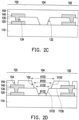
- a second metal layer 140 and a second insulation layer 150 may be subsequently formed on the first insulation layer 130.
- a method of fabricating the second metal layer 140 is similar to the method of fabricating the first metal layer 120, and a layout of the second metal layer 140 may be different from a layout of the first metal layer 120 to realize a required electrical transmission path. At least a portion of the second metal layer 140 is located in the first hole 134 and electrically connected to the first metal layer 120 through the first hole 134.
- a method of forming the second insulation layer 150 is similar to a method of forming the first insulation layer 130. The second insulation layer 150 covers the second metal layer 140 and covers the first insulation layer 130 beyond the second metal layer 140.
- the second metal layer 140 is located between the first insulation layer 130 and the second insulation layer 150.
- the second insulation layer 150 may extend to the first opening 132 of the first insulation layer 130 to contact the substrate 110 below the first insulation layer 130.
- a material of the second insulation layer 150 may be similar to or the same as a material of the first insulation layer 130.
- the second insulation layer 150 is patterned to form a second opening 152 and a second hole 154.
- a method of patterning the second insulation layer 150 may be similar to the method of patterning the first insulation layer 130.
- the second hole 154 may expose a portion of the second metal layer 140 to provide a path for mutual electrical connection of the second metal layer 140 and a metal layer that is further formed.
- the second opening 152 corresponds to the first opening 132, and the second opening 152 exposes the first opening 132.
- the second opening 152 has an outline in the shape of an inverted trapezoid that is similar to the outline of the first opening 132, and a size of the second opening 152 is greater than a size of the first opening 132.
- the second opening 152 may expose the first insulation layer 130 at the sidewall S132 of the first opening 132.
- a width B152 of a lower bottom of the second opening 152 may be less than a width U152 of an upper bottom of the second opening 152, and the width B152 of the lower bottom of the second opening 152 may be greater than the width U132 of the upper bottom of the first opening 132.
- a minimum of a width of the second opening 152 may be greater than a maximum of a width of the first opening 132.
- the first opening 132 and the second opening 152 may be connected to form a through hole with a stair-shaped (or step-shaped) outline.
- the sidewall S132 of the first opening 132, the top surface T130 of the first insulation layer 130 and the sidewall S152 of the second opening 152 form a stair-shaped (or step-shaped) outline which defines the through hole passing through the first insulation layer 130 and the second insulation layer 150.
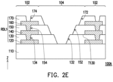
- a third metal layer 160 and a third insulation layer 170 are further sequentially formed on the second insulation layer 150 to form a connection element RDL1 of an electronic device 100A.
- the first insulation layer 130, the first metal layer 140, the second insulation layer 150, the third metal layer 160 and the third insulation layer 170 may be stack in sequence on the substrate 110 along a Z direction which is the normal direction of the electronic device 100A.
- a method of fabricating the third metal layer 160 is similar to the method of fabricating the first metal layer 120 and the second metal layer 140, and a method of fabricating the third insulation layer 170 is similar to the method of fabricating the first insulation layer 130 and the second insulation layer 150.
- the third metal layer 160 may extend to the second hole 154 of the second insulation layer 150, and the third insulation layer 170 may be patterned to have a third opening 172.
- the third metal layer 160 is electrically connected to the second metal layer 140 through the second hole 154.
- the third opening 172 of the third insulation layer 170 exposes the second opening 152 of the second insulation layer 150.
- a size of the third opening 172 is greater than the size of the second opening 152.
- a minimum of a width of the third opening 172 is greater than a maximum of the width of the second opening 152, and the third opening 172 exposes a sidewall of the second insulation layer 150 at the second opening 152.
- the first opening 132, the second opening 152, and the third opening 172 may form a through hole with a stair-shaped outline.
- the electronic device 100A includes the connection element RDL1.
- the connection element RDL1 includes multiple insulation layers, such as the first insulation layer 130 and the second insulation layer 150.
- the first insulation layer 130 has the first opening 132.
- the sidewall S132 of the first insulation layer 130 at the first opening 132 has the roughness different from the roughness of the top surface T130 of the first insulation layer 130.
- the second insulation layer 150 is disposed on the first insulation layer 130 and has the second opening 152.
- the second opening 152 exposes the first insulation layer 130 at the sidewall S132 of the first opening 132.
- the first opening 132 and the second opening 152 may provide a channel to release the stress, preventing structural deformation or warpage caused by the stress in the fabricating process. As a result, a yield in the process of fabricating the electronic device 100A may be enhanced due to the first opening 132 and the second opening 152.
- positions of the first opening 132, the second opening 152, and the third opening 172 may be set in advance. In some embodiments, the positions of the first opening 132, the second opening 152, and the third opening 172 may be adjusted according to an actual state of the device. For example, before each insulation layer is fabricated, flatness of the entire device is inspected, and the positions of the first opening 132, the second opening 152, and the third opening 172 are determined according to an inspection result. For example, before the insulation layer is fabricated, the flatness of the entire device may be inspected by adopting the automated optical inspection system.
- first opening 132, the second opening 152, and the third opening 172 may be disposed at positions where warpage occurs or relatively severe warpage occurs according to the inspection result. In this way, in a further process, inaccurate positioning or uneven film thickness due to warpage of the structure may not occur. In some embodiments, if the flatness inspection result shows that there is no obvious warpage or deformation, a buffer opening may not be formed on a corresponding insulation layer.
- connection element RDL1 may serve as the redistribution layer of the element to provide a required conducting transmission path.
- the redistribution layer may include thin film transistor, ESD, capacitance or other active element, but not limited to.
- the connection element RDL1 further includes the first metal layer 120, the second metal layer 140, and the third metal layer 160.
- the first metal layer 120 is disposed between the substrate 110 and the first insulation layer 130.
- the second metal layer 140 is disposed between the first insulation layer 130 and the second insulation layer 150.
- the third metal layer 160 is disposed between the second insulation layer 150 and the third insulation layer 170.
- the first hole 134 of the first insulation layer 130 exposes a portion of the first metal layer 120.
- the second metal layer 140 may extend to the first hole 134 of the first insulation layer 130 to be electrically connected to the first metal layer 120.
- the third metal layer 160 may extend to the second hole 154 of the second insulation layer 150 to be electrically connected to the second metal layer 140.
- a third hole 174 of the third insulation layer 170 may expose a portion of the third metal layer 160.
- a layer number of metal layers and a layer number of insulation layers may be adjusted according to required layout planning. In FIG. 2E , for example, four metal layers and four insulation layers are taken as an example for description.
- the electronic device 100A may further include an electronic element, such as a semiconductor chip.
- the semiconductor chip may be disposed on the substrate 110 and electrically connected to the connection element RDL1.
- the semiconductor chip may be connected to the substrate 110 after the fabrication of the connection element RDL1 is completed, which means that a fabricating method of RDL first is adopted.
- the semiconductor chip disposed on the substrate 110 may be a die of chip packaging.
- the electronic device 100A may further include a packaging material that is not shown, such as a molding compound, and the packaging material includes the semiconductor chip.
- FIG. 3A to FIG. 3E are schematic diagrams of some steps of a method of fabricating an electronic device according to some embodiments of the disclosure. Structures shown in FIG. 3A to FIG. 3E correspond to a cross-sectional view of the electronic device along the line I-I in FIG. 1 ; however, the method of fabricating the electronic device is not limited thereto.
- the substrate 110 is provided.
- a semiconductor chip 220 is attached to the substrate 110, and a first insulation layer 230 is formed on the substrate 110.
- the semiconductor chip 220 may be attached to the substrate 110 through an adhesion layer (not shown), and corresponding to a layout of FIG. 1 , the semiconductor chip 220 may be located in the element areas 102.
- the non-element areas 104 are present between the adjacent element areas 102.
- the semiconductor chip 220 may be attached to the substrate 110 with an active surface facing upwards or attached to the substrate 110 with the active surface facing downwards.
- the first insulation layer 230 may encapsulate the semiconductor chip 220.
- a material of the first insulation layer 230 may include a packaging material, such as a molding compound, epoxy, and the like.
- the first insulation layer 230 may include matrix and a filling material distributed in the matrix.
- an insulation material of the first insulation layer 230 may first completely cover the semiconductor chip 220. Then, a polishing process is performed to expose a bonding element 222 on the semiconductor chip 220.
- the first insulation layer 230 may have a first hole 230V so that the bonding element 222 on the semiconductor chip 220 may penetrate the first insulation layer 230 and be exposed.
- the first insulation layer 230 is patterned to form a first opening 232 in the non-element areas 104.
- a method of patterning the first insulation layer 230 may include laser drilling.
- a method of forming the first opening 232 is similar to the method of forming the first opening 132.
- a cleaning process is further performed to remove detritus generated in the process of laser drilling.
- the first opening 232 formed through laser drilling may have an outline in the shape of an inverted trapezoid.
- a width B132 of a lower bottom of the first opening 232 is less than a width U232 of an upper bottom of the first opening 232.
- roughness of a sidewall S232 of the first insulation layer 230 at the first opening 232 may be greater than roughness of a top surface T230 of the first insulation layer 230.
- surface roughness of the sidewall S232 may be 1500 nm to 6000 nm
- surface roughness of the top surface T230 may be 600 nm to 1300 nm.
- an included angle ⁇ 2 between the sidewall S232 of the first insulation layer 230 at the first opening 232 and a bottom surface B230 of the first insulation layer 230 may be greater than 30 degrees and less than or equal to 75 degrees.
- the angle range of the sidewall S232, the rough surface of the sidewall S232, or a combination thereof may enhance the attaching between the metal material subsequently formed and the first insulation layer 230.
- a surface of the sidewall S232 may have a scorch material, but the scorch material may be removed in the cleaning process. Similar to the sidewall S132, the scorch material may include carbon, but the disclosure is not limited thereto.
- a first metal layer 240 and a second insulation layer 250 are sequentially formed on the first insulation layer 230.
- the first metal layer 240 may be electrically connected to the semiconductor chip 220 through the corresponding bonding element 222.
- the second insulation layer 250 may be entirely formed on the substrate 110 to cover the first metal layer 240 and the first insulation layer 230.
- the second insulation layer 250 may extend into the first opening 232 to contact the substrate 110.
- the second insulation layer 250 is patterned to form a second opening 252 and a second hole 254.
- a method similar to the method of patterning the first insulation layer 130 in the previous embodiments may be adopted to pattern the second insulation layer 250.
- the second opening 252 may penetrate the first opening 232 to form a through hole.
- a size of the second opening 252 may be greater than a size of the first opening 232 so that the sidewall S232 of the first insulation layer 230 at the first opening 232 may be completely exposed.
- a width B252 of a lower bottom of the second opening 252 may be less than a width U252 of an upper bottom of the second opening 252, and the width B252 of the lower bottom of the second opening 252 may be greater than the width U232 of the upper bottom of the first opening 232. That is, a minimum of a width of the second opening 252 may be greater than a maximum of a width of the first opening 232. In this way, the first opening 232 and the second opening 252 may be connected to form a through hole with a stair-shaped outline.
- a second metal layer 260, a third insulation layer 270, a third metal layer 280, and a fourth insulation layer 290 are sequentially formed on the second insulation layer 250 to form an electronic device 100B having a connection element RDL2.
- the first insulation layer 230, the first metal layer 240, the second insulation layer 250, the second metal layer 260, the third insulation layer 270, the third metal layer 280, and the fourth insulation layer 290 may be stack in sequence on the substrate 110 along a Z direction which is the normal direction of the electronic device 100B.
- the connection element RDL2 may serve as a redistribution layer to realize a required electrical transmission path of the semiconductor chip 220.
- connection element RDL2 is fabricated after the semiconductor chip 220 is attached to the substrate 110.
- a fabricating method of chip first is adopted; however, the disclosure is not limited thereto.
- a method of fabricating the third insulation layer 270 and the fourth insulation layer 290 is similar to the method of fabricating the first insulation layer 230 and the second insulation layer 250.
- the third insulation layer 270 may be patterned to have a third opening 272, and the fourth insulation layer 290 may be patterned to have a fourth opening 292.
- the third opening 272 penetrates the first opening 232 and the second opening 252, and the fourth opening 292 penetrates the first opening 232, the second opening 252, the third opening 272 to form a through hole.
- the through hole formed through the fourth opening 292 penetrating the first opening 232, the second opening 252, and the third opening 272 has a stair-shaped outline.
- the first opening 232, the second opening 252, the third opening 272, and the fourth opening 292 may serve as a buffer structure.
- stress generated due to a change in temperature or pressure may be released so that it is not likely to cause warpage of the substrate 110.
- favorable flatness may be maintained so that accuracy of a patterning process may be enhanced to increase a yield in the fabricating process.
- the insulation layer in the connection element may be separated to provide a buffer. Therefore, in the fabricating process, the warpage of the electronic device due to the stress is not likely to occur so that the yield in the fabricating process of the electronic device may be increased.
Landscapes
- Internal Circuitry In Semiconductor Integrated Circuit Devices (AREA)
- Engineering & Computer Science (AREA)
- Manufacturing & Machinery (AREA)
- Semiconductor Integrated Circuits (AREA)
- Production Of Multi-Layered Print Wiring Board (AREA)
Abstract
Description
- The disclosure relates to an electronic device and a method of fabricating an electronic device.
- In a process of fabricating an electronic device, due to different physical properties of different materials, such as a coefficient of thermal expansion, warpage of products caused by the difference is an issue that has to be addressed.
- The disclosure provides an electronic device with good quality.
- The disclosure provides a method of fabricating an electronic device capable of effectively avoiding warpage in a fabricating process of the electronic device.
- According to the embodiment of the disclosure, an electronic device includes a connection element. The connection element includes a first insulation layer and a second insulation layer. The first insulation layer has a first opening. A sidewall of the first insulation layer at the first opening has roughness different from roughness of a top surface of the first insulation layer. The second insulation layer is disposed on the first insulation layer, and the second insulation layer has a second opening. The sidewall of the first insulation layer at the first opening is exposed by the second opening.
- According to the embodiment of the disclosure, a method of fabricating an electronic device includes the following. A substrate is provided. A first insulation layer is formed on the substrate. The first insulation layer is patterned to form a first opening. A second insulation layer is formed on the first insulation layer. The second insulation layer extends to the first opening, and in a cross-sectional view, a width of a lower bottom of the first opening is less than a width of an upper bottom of the first opening.
- According to the embodiment of the disclosure, a method of fabricating an electronic device includes the following. A substrate is provided. A first insulation layer is formed on the substrate. The first insulation layer is patterned to form a first opening. A second insulation layer is formed on the first insulation layer. The second insulation layer is patterned to form a second opening corresponding to the first opening. In a cross-sectional view, a width of a lower bottom of the first opening is less than a width of an upper bottom of the first opening, and the width of the upper bottom of the first opening is less than a width of a lower bottom of the second opening.
- In order to make the aforementioned features and advantages of the disclosure comprehensible, embodiments accompanied with drawings are described in detail below.
- The accompanying drawings are included to provide a further understanding of the disclosure, and are incorporated in and constitute a part of this specification. The drawings illustrate embodiments of the disclosure and, together with the description, serve to explain the principles of the disclosure.
-
FIG. 1 is a schematic diagram of an electronic device according to an embodiment of the disclosure. -
FIG. 2A to FIG. 2E are schematic diagrams of some steps of a method of fabricating an electronic device according to some embodiments of the disclosure in a cross-section view. -
FIG. 3A to FIG. 3E are schematic diagrams of some steps of a method of fabricating an electronic device according to some embodiments of the disclosure in a cross-section view. - Reference will now be made in detail to the present exemplary embodiments of the disclosure, examples of which are illustrated in the accompanying drawings. Wherever possible, the same reference numerals are used in the drawings and the description to refer to the same or like parts.
- In the following specification and claims, words such as "including", "containing", and "having" are open-ended words, so they should be interpreted as meaning "containing but not limited to...".
- A structure (or layer type, component, substrate) being located on/above another structure (or layer type, element, substrate) or a structure (or layer type, component, substrate) being connected to another structure (or layer type, element, substrate) described in this disclosure may refer to two structures being adjacent and directly connected to each other, or may refer to two structures being adjacent but not directly connected to each other. An indirect connection means that there is at least one intermediary structure (or intermediary layer, intermediary component, intermediary substrate, or intermediary interval) between two structures, and the lower lateral surface of a structure is adjacent or directly connected to the upper lateral surface of an intermediary structure, and the upper lateral surface of another structure is adjacent or directly connected to the lower lateral surface of the intermediary structure. The intermediary structure may be a monolayer or multi-layer physical structure or a non-physical structure, and the disclosure is not limited thereto. In this disclosure, when a structure is "above" another structure, it may mean that a certain structure is "directly" on another structure, or that a certain structure is "indirectly" on another structure, that is, there is at least one structure between said certain structure and said another structure.
- Although the terms "first", "second", "third"... may be used to describe various constituent elements, the constituent elements are not limited to these terms. These terms are only used to distinguish a single constituent element from other constituent elements in the specification. The same terms may not be used in the claims, and may be replaced with first, second, third... according to a declared order of the elements in the claims. Accordingly, in following description of the specification, the first constituent element may be the second constituent element in the claims.
- In the specification, the terms "about", "around", "substantial", and "approximate", generally refers to be within 10%, or within 5%, or within 3%, or within 2%, or within 1%, or within 0.5% of a given value or range. The quantity given here is an approximate quantity, i.e., in the absence of a specific description of "about", "around", "substantial", and "approximate", the meanings of "about", "around", "substantial", and "approximate" may still be implied. Moreover, the terms "a range from a first value to a second value" and "a range between a first value and a second value" indicate that the range includes the first value, the second value, and other values in between.
- The terms "electrically connect" and "couple" described in the disclosure include any direct and indirect electrical connection. In a case of direct electrical connection, end points of two circuits are directly connected or connected to each other with a conductive line. In a case of indirect electrical connection, there is a switch, a diode, a capacitor, inductance, a resistor, or other suitable component, or a combination of the components above between the end points of the two circuits; however, the disclosure is not limited thereto.
- In the disclosure, the thickness, the length, and the width may be measured by an optical microscope, and the thickness may be measured based on a cross-sectional image in an electron microscope, but the disclosure is not limited thereto. In addition, there may be a certain error between any two values or directions used for comparison. When a first value is equal to a second value, it implies that there may be an error of 10%, 5%, or 3% between the first value and the second value.
- It should be noted that the embodiments listed below can replace, recombine, and mix features in several different embodiments to achieve other embodiments without departing from the principle of the disclosure. The features of the embodiments may be arbitrarily mixed and combined as long as they do not depart from or conflict with the spirit of the disclosure.
-
FIG. 1 is a schematic diagram of an electronic device according to an embodiment of the disclosure. In some embodiments, theelectronic device 100 may be a high frequency element, a light emitting element, a display device, a titled device, a packaging device, and the like. In some embodiments, theelectronic device 100 may be flexible or foldable. Anelectronic device 100 hasmultiple element areas 102 and multiplenon-element areas 104. Theelement areas 102 are arranged into an array and are separated from each other, and thenon-element areas 104 are distributed among theelement areas 102. In some embodiments, at least a chip, a redistribution layer, and a packaging material are provided in theelement areas 102. The chip may be a light emitting chip, a semiconductor chip, and the like. In some embodiments, the semiconductor chip may define an electronic circuit combined with an active element, a passive element, or a combination thereof, such as a logic circuit, a memory circuit, and the like. In some embodiments, theelectronic device 100 may be a high-frequency element, a light emitting element, a packaging element, and the like. Thenon-element areas 104 may include scribe lines, and multiple independent electronic devices of theelectronic device 100 may be separated along the scribe lines. In some embodiments, after cutting, a structure of thenon-element areas 104 may be partially kept in the independent electronic devices or may not be present in the independent electronic devices. - In some embodiments, an individual component in the
electronic device 100 is mainly supported by asubstrate 110. In addition, a required connection element may be fabricated on thesubstrate 110 to realize required electrical connection of each component. Here, the connection element may be viewed as a redistribution layer; however, the disclosure is not limited thereto. Thesubstrate 110 may be a glass substrate, a silicon substrate, a sapphire substrate, and the like, and have a panel level size. For example, thesubstrate 110 may be a G3.5 glass substrate with a size of 610 mm×720 mm; however, the disclosure is not limited thereto. In other embodiments, thesubstrate 110 may be a G3 glass substrate, a G4 glass substrate, a G4.5 glass substrate, a G5 glass substrate, a G5.5 glass substrate, or a glass substrate of further generation. In the embodiment, the chip is connected to the panel level substrate. The redistribution layer is fabricated on the panel level substrate, and the chip is packaged. Hence, the embodiment may serve as an application of fan out panel level packaging (FOPLP). Since thepanel level substrate 110 is adopted in the fan out panel level packaging process, compared to wafer level packaging, the productivity may be greatly increased. At the same time, thepanel level substrate 110 has a rectangle outline, compared to wafer level packaging, the utilization ratio of thesubstrate 110 may also be greatly increased. As a result, theelectronic device 100 may be configured to realize the requirement of the high productivity. -
FIG. 2A to FIG. 2E are schematic diagrams of some steps of a method of fabricating an electronic device according to some embodiments of the disclosure. Structures shown inFIG. 2A to FIG. 2E correspond to a cross-sectional view along a line I-I inFIG. 1 ; however, the method of fabricating the electronic device is not limited thereto. InFIG. 2A , thesubstrate 110 is first provided. Afirst metal layer 120 is formed on thesubstrate 110, and afirst insulation layer 130 is formed on thefirst metal layer 120. Thefirst metal layer 120 may be distributed in theelement areas 102 to establish a required electrical transmission path in theelement areas 102. In some embodiments, a method of fabricating thefirst metal layer 120 may include depositing a metal material on thesubstrate 110 and patterning the metal material to form thefirst metal layer 120. A method of patterning the metal material may include photolithography or other replaceable method. - A method of fabricating the
first insulation layer 130 may include forming an insulation material on thesubstrate 110 so that the insulation material covers thefirst metal layer 120 and covers thesubstrate 110. Thefirst insulation layer 130 may completely cover an area of thesubstrate 110. In some embodiments, the insulation material of thefirst insulation layer 130 may include an ajinomoto build-up film (ABF) adhesive, epoxy, a molding compound, other build up materials, and the like; however, the disclosure is not limited thereto. In some embodiments, thefirst insulation layer 130 may be a thin film fabricated in advance, and thefirst insulation layer 130 may be attached to thesubstrate 110 in a bonding manner and cover thefirst metal layer 120. In addition, thefirst insulation layer 130 in a shape of a thin film is soft enough to extend along an outline of thefirst metal layer 120. In some embodiments, thefirst insulation layer 130 may include matrix and a filling material distributed in the matrix. The filling material includes, for example, a silicon dioxide filling material, glass fiber, and the like. - In
FIG. 2B , next, thefirst insulation layer 130 is patterned to form afirst opening 132 and afirst hole 134. In the description, the term "hole" may be understood as a structure that is formed in theelement areas 102 after patterning the insulation layer and may be filled with and/or covered by a further film layer, and the term "opening" may be understood as a structure that is formed in thenon-element areas 104 after patterning the insulation layer and may be exposed in a further process; however, the disclosure is not limited thereto. A method of patterning thefirst insulation layer 130 includes laser drilling. In some embodiments, a laser beam of laser drilling may have a wavelength ranging from 266 nm to 355 nm; however, the disclosure is not limited thereto. Specifically, parameters such as energy or a focal length of the laser beam of laser drilling may be adjusted according to a film layer that is patterned and a pattern that is expected to be formed. After laser drilling, a cleaning process is performed to clean remaining detritus. In the cleaning process, for example, the remaining detritus is cleaned by using plasma or a suitable detergent. In some embodiments, before executing laser drilling, flatness of the device may be first inspected. For example, the flatness of the entire device is inspected by adopting an automated optical inspection (AOI) system. In this way, laser drilling may be executed in an area that is relatively not flat to form thefirst opening 132. In other words, a position of thefirst opening 132 may be adjusted according to an actual state of the device. In addition, thefirst hole 134 is located on thefirst metal layer 120 to expose a portion of thefirst metal layer 120. - In some embodiments, the
first insulation layer 130 that undergoes laser drilling may have a rough surface. Hence, a sidewall S132 of thefirst insulation layer 130 at thefirst opening 132 and a sidewall S134 of thefirst insulation layer 130 at thefirst hole 134 may have roughness different from roughness of a top surface T130 of thefirst insulation layer 130. Specifically, the sidewall S132 and the sidewall S134 are rougher than the top surface T130. Namely, the roughness of the sidewall S134 of thefirst insulation layer 130 at thefirst hole 134 is greater than the roughness of the top surface T130 of thefirst insulation layer 130, and the roughness of the sidewall S132 of thefirst insulation layer 130 at thefirst opening 132 is greater than the roughness of the top surface T130 of thefirst insulation layer 130. In some embodiments, surface roughness of the sidewall S132 and surface roughness of the sidewall S134 may be 1500 nm to 6000 nm, and surface roughness of the top surface T130 may be 600 nm to 1300 nm. In addition, an outline of thefirst opening 132 and an outline of thefirst hole 134 may be in a shape of an inverted trapezoid in a cross section view. For example, a width B132 of a lower bottom of thefirst opening 132 is less than a width U132 of an upper bottom of thefirst opening 132, and a width of a lower bottom of thefirst hole 134 is less than a width of an upper bottom of thefirst hole 134. The sidewall S132 of thefirst insulation layer 130 at thefirst opening 132 and the sidewall S134 of thefirst insulation layer 130 at thefirst hole 134 may be approximately arc-shaped in a cross-sectional view, but they can also be a straight line. In addition, an included angle θ1 between the sidewall S132 of thefirst insulation layer 130 at thefirst opening 132 and a bottom surface B130 of thefirst insulation layer 130 may be greater than 30 degrees and less than or equal to 75 degrees. At the same time, thefirst hole 134 may have a similar inclined sidewall. In some embodiments, since laser drilling is adopted, a surface of the sidewall S132 and a surface of the sidewall S134 may have a scorch material, but the scorch material may be removed in the cleaning process. For example, the scorch material may include carbon. In some embodiments, the sidewall S132 and the sidewall S134 can be analyzed using a scanning electron microscope (SEM) or an energy dispersive spectroscopy (EDS) to determine the component of the scorch material. For example, through the image of the sidewall S132 or the sidewall S134 captured by SEM, debris separated from the body of thefirst insulation layer 130 may be seen and the material of the debris analyzed by using the EDS includes carbon. - In
FIG. 2C , asecond metal layer 140 and asecond insulation layer 150 may be subsequently formed on thefirst insulation layer 130. A method of fabricating thesecond metal layer 140 is similar to the method of fabricating thefirst metal layer 120, and a layout of thesecond metal layer 140 may be different from a layout of thefirst metal layer 120 to realize a required electrical transmission path. At least a portion of thesecond metal layer 140 is located in thefirst hole 134 and electrically connected to thefirst metal layer 120 through thefirst hole 134. A method of forming thesecond insulation layer 150 is similar to a method of forming thefirst insulation layer 130. Thesecond insulation layer 150 covers thesecond metal layer 140 and covers thefirst insulation layer 130 beyond thesecond metal layer 140. Hence, thesecond metal layer 140 is located between thefirst insulation layer 130 and thesecond insulation layer 150. In addition, thesecond insulation layer 150 may extend to thefirst opening 132 of thefirst insulation layer 130 to contact thesubstrate 110 below thefirst insulation layer 130. A material of thesecond insulation layer 150 may be similar to or the same as a material of thefirst insulation layer 130. - In
FIG. 2D , thesecond insulation layer 150 is patterned to form asecond opening 152 and asecond hole 154. In some embodiments, a method of patterning thesecond insulation layer 150 may be similar to the method of patterning thefirst insulation layer 130. Thesecond hole 154 may expose a portion of thesecond metal layer 140 to provide a path for mutual electrical connection of thesecond metal layer 140 and a metal layer that is further formed. Thesecond opening 152 corresponds to thefirst opening 132, and thesecond opening 152 exposes thefirst opening 132. - In the embodiment, the
second opening 152 has an outline in the shape of an inverted trapezoid that is similar to the outline of thefirst opening 132, and a size of thesecond opening 152 is greater than a size of thefirst opening 132. Hence, thesecond opening 152 may expose thefirst insulation layer 130 at the sidewall S132 of thefirst opening 132. For example, a width B152 of a lower bottom of thesecond opening 152 may be less than a width U152 of an upper bottom of thesecond opening 152, and the width B152 of the lower bottom of thesecond opening 152 may be greater than the width U132 of the upper bottom of thefirst opening 132. That is, a minimum of a width of thesecond opening 152 may be greater than a maximum of a width of thefirst opening 132. In this way, thefirst opening 132 and thesecond opening 152 may be connected to form a through hole with a stair-shaped (or step-shaped) outline. For example, the sidewall S132 of thefirst opening 132, the top surface T130 of thefirst insulation layer 130 and the sidewall S152 of thesecond opening 152 form a stair-shaped (or step-shaped) outline which defines the through hole passing through thefirst insulation layer 130 and thesecond insulation layer 150. - In
FIG. 2E , after the step ofFIG. 2D , athird metal layer 160 and athird insulation layer 170 are further sequentially formed on thesecond insulation layer 150 to form a connection element RDL1 of anelectronic device 100A. Thefirst insulation layer 130, thefirst metal layer 140, thesecond insulation layer 150, thethird metal layer 160 and thethird insulation layer 170 may be stack in sequence on thesubstrate 110 along a Z direction which is the normal direction of theelectronic device 100A. A method of fabricating thethird metal layer 160 is similar to the method of fabricating thefirst metal layer 120 and thesecond metal layer 140, and a method of fabricating thethird insulation layer 170 is similar to the method of fabricating thefirst insulation layer 130 and thesecond insulation layer 150. For example, thethird metal layer 160 may extend to thesecond hole 154 of thesecond insulation layer 150, and thethird insulation layer 170 may be patterned to have athird opening 172. Thethird metal layer 160 is electrically connected to thesecond metal layer 140 through thesecond hole 154. Thethird opening 172 of thethird insulation layer 170 exposes thesecond opening 152 of thesecond insulation layer 150. In the embodiment, a size of thethird opening 172 is greater than the size of thesecond opening 152. For example, a minimum of a width of thethird opening 172 is greater than a maximum of the width of thesecond opening 152, and thethird opening 172 exposes a sidewall of thesecond insulation layer 150 at thesecond opening 152. Hence, thefirst opening 132, thesecond opening 152, and thethird opening 172 may form a through hole with a stair-shaped outline. - In
FIG. 2E , theelectronic device 100A includes the connection element RDL1. The connection element RDL1 includes multiple insulation layers, such as thefirst insulation layer 130 and thesecond insulation layer 150. Thefirst insulation layer 130 has thefirst opening 132. The sidewall S132 of thefirst insulation layer 130 at thefirst opening 132 has the roughness different from the roughness of the top surface T130 of thefirst insulation layer 130. Thesecond insulation layer 150 is disposed on thefirst insulation layer 130 and has thesecond opening 152. Thesecond opening 152 exposes thefirst insulation layer 130 at the sidewall S132 of thefirst opening 132. In a process of fabricating theelectronic device 100A, if stress occurs, thefirst opening 132 and thesecond opening 152 may provide a channel to release the stress, preventing structural deformation or warpage caused by the stress in the fabricating process. As a result, a yield in the process of fabricating theelectronic device 100A may be enhanced due to thefirst opening 132 and thesecond opening 152. - In some embodiments, when fabricating the
electronic device 100A, positions of thefirst opening 132, thesecond opening 152, and thethird opening 172 may be set in advance. In some embodiments, the positions of thefirst opening 132, thesecond opening 152, and thethird opening 172 may be adjusted according to an actual state of the device. For example, before each insulation layer is fabricated, flatness of the entire device is inspected, and the positions of thefirst opening 132, thesecond opening 152, and thethird opening 172 are determined according to an inspection result. For example, before the insulation layer is fabricated, the flatness of the entire device may be inspected by adopting the automated optical inspection system. In addition, thefirst opening 132, thesecond opening 152, and thethird opening 172 may be disposed at positions where warpage occurs or relatively severe warpage occurs according to the inspection result. In this way, in a further process, inaccurate positioning or uneven film thickness due to warpage of the structure may not occur. In some embodiments, if the flatness inspection result shows that there is no obvious warpage or deformation, a buffer opening may not be formed on a corresponding insulation layer. - The connection element RDL1 may serve as the redistribution layer of the element to provide a required conducting transmission path. In one embodiment, the redistribution layer may include thin film transistor, ESD, capacitance or other active element, but not limited to. Specifically, the connection element RDL1 further includes the
first metal layer 120, thesecond metal layer 140, and thethird metal layer 160. Thefirst metal layer 120 is disposed between thesubstrate 110 and thefirst insulation layer 130. Thesecond metal layer 140 is disposed between thefirst insulation layer 130 and thesecond insulation layer 150. Thethird metal layer 160 is disposed between thesecond insulation layer 150 and thethird insulation layer 170. Thefirst hole 134 of thefirst insulation layer 130 exposes a portion of thefirst metal layer 120. Thesecond metal layer 140 may extend to thefirst hole 134 of thefirst insulation layer 130 to be electrically connected to thefirst metal layer 120. Similarly, thethird metal layer 160 may extend to thesecond hole 154 of thesecond insulation layer 150 to be electrically connected to thesecond metal layer 140. In addition, athird hole 174 of thethird insulation layer 170 may expose a portion of thethird metal layer 160. A layer number of metal layers and a layer number of insulation layers may be adjusted according to required layout planning. InFIG. 2E , for example, four metal layers and four insulation layers are taken as an example for description. - In addition, although it is not shown in the drawings, the
electronic device 100A may further include an electronic element, such as a semiconductor chip. The semiconductor chip may be disposed on thesubstrate 110 and electrically connected to the connection element RDL1. The semiconductor chip may be connected to thesubstrate 110 after the fabrication of the connection element RDL1 is completed, which means that a fabricating method of RDL first is adopted. In some embodiments, the semiconductor chip disposed on thesubstrate 110 may be a die of chip packaging. Hence, theelectronic device 100A may further include a packaging material that is not shown, such as a molding compound, and the packaging material includes the semiconductor chip. -
FIG. 3A to FIG. 3E are schematic diagrams of some steps of a method of fabricating an electronic device according to some embodiments of the disclosure. Structures shown inFIG. 3A to FIG. 3E correspond to a cross-sectional view of the electronic device along the line I-I inFIG. 1 ; however, the method of fabricating the electronic device is not limited thereto. InFIG. 3A , thesubstrate 110 is provided. Asemiconductor chip 220 is attached to thesubstrate 110, and afirst insulation layer 230 is formed on thesubstrate 110. Thesemiconductor chip 220 may be attached to thesubstrate 110 through an adhesion layer (not shown), and corresponding to a layout ofFIG. 1 , thesemiconductor chip 220 may be located in theelement areas 102. Thenon-element areas 104 are present between theadjacent element areas 102. In some embodiments, thesemiconductor chip 220 may be attached to thesubstrate 110 with an active surface facing upwards or attached to thesubstrate 110 with the active surface facing downwards. Thefirst insulation layer 230 may encapsulate thesemiconductor chip 220. In some embodiments, a material of thefirst insulation layer 230 may include a packaging material, such as a molding compound, epoxy, and the like. In some embodiments, thefirst insulation layer 230 may include matrix and a filling material distributed in the matrix. In addition, when thefirst insulation layer 230 is formed, an insulation material of thefirst insulation layer 230 may first completely cover thesemiconductor chip 220. Then, a polishing process is performed to expose abonding element 222 on thesemiconductor chip 220. Hence, thefirst insulation layer 230 may have afirst hole 230V so that thebonding element 222 on thesemiconductor chip 220 may penetrate thefirst insulation layer 230 and be exposed. However, it is not necessary to adopt an additional process to fabricate thefirst hole 230V. - In
FIG. 3B , next, thefirst insulation layer 230 is patterned to form afirst opening 232 in thenon-element areas 104. In the embodiment, a method of patterning thefirst insulation layer 230 may include laser drilling. In other words, a method of forming thefirst opening 232 is similar to the method of forming thefirst opening 132. Hence, in the embodiment, after thefirst insulation layer 230 is patterned through laser drilling, a cleaning process is further performed to remove detritus generated in the process of laser drilling. In the embodiment, thefirst opening 232 formed through laser drilling may have an outline in the shape of an inverted trapezoid. A width B132 of a lower bottom of thefirst opening 232 is less than a width U232 of an upper bottom of thefirst opening 232. In the embodiment, roughness of a sidewall S232 of thefirst insulation layer 230 at thefirst opening 232 may be greater than roughness of a top surface T230 of thefirst insulation layer 230. In some embodiments, surface roughness of the sidewall S232 may be 1500 nm to 6000 nm, and surface roughness of the top surface T230 may be 600 nm to 1300 nm. In addition, an included angle θ2 between the sidewall S232 of thefirst insulation layer 230 at thefirst opening 232 and a bottom surface B230 of thefirst insulation layer 230 may be greater than 30 degrees and less than or equal to 75 degrees. The angle range of the sidewall S232, the rough surface of the sidewall S232, or a combination thereof may enhance the attaching between the metal material subsequently formed and thefirst insulation layer 230. In some embodiments, since laser drilling is adopted, a surface of the sidewall S232 may have a scorch material, but the scorch material may be removed in the cleaning process. Similar to the sidewall S132, the scorch material may include carbon, but the disclosure is not limited thereto. - In
FIG. 3C , afirst metal layer 240 and a second insulation layer 250 are sequentially formed on thefirst insulation layer 230. For a method of forming thefirst metal layer 240, the description of a method of forming thefirst metal layer 120 in the previous embodiments may be referred to. Thefirst metal layer 240 may be electrically connected to thesemiconductor chip 220 through thecorresponding bonding element 222. The second insulation layer 250 may be entirely formed on thesubstrate 110 to cover thefirst metal layer 240 and thefirst insulation layer 230. For example, in a process ofFIG. 3C , the second insulation layer 250 may extend into thefirst opening 232 to contact thesubstrate 110. - Next, in
FIG. 3D , the second insulation layer 250 is patterned to form asecond opening 252 and asecond hole 254. A method similar to the method of patterning thefirst insulation layer 130 in the previous embodiments may be adopted to pattern the second insulation layer 250. In the embodiment, thesecond opening 252 may penetrate thefirst opening 232 to form a through hole. A size of thesecond opening 252 may be greater than a size of thefirst opening 232 so that the sidewall S232 of thefirst insulation layer 230 at thefirst opening 232 may be completely exposed. For example, a width B252 of a lower bottom of thesecond opening 252 may be less than a width U252 of an upper bottom of thesecond opening 252, and the width B252 of the lower bottom of thesecond opening 252 may be greater than the width U232 of the upper bottom of thefirst opening 232. That is, a minimum of a width of thesecond opening 252 may be greater than a maximum of a width of thefirst opening 232. In this way, thefirst opening 232 and thesecond opening 252 may be connected to form a through hole with a stair-shaped outline. - In
FIG. 3E , a second metal layer 260, a third insulation layer 270, a third metal layer 280, and afourth insulation layer 290 are sequentially formed on the second insulation layer 250 to form anelectronic device 100B having a connection element RDL2. Thefirst insulation layer 230, thefirst metal layer 240, the second insulation layer 250, the second metal layer 260, the third insulation layer 270, the third metal layer 280, and thefourth insulation layer 290 may be stack in sequence on thesubstrate 110 along a Z direction which is the normal direction of theelectronic device 100B. The connection element RDL2 may serve as a redistribution layer to realize a required electrical transmission path of thesemiconductor chip 220. In the embodiment, the connection element RDL2 is fabricated after thesemiconductor chip 220 is attached to thesubstrate 110. Hence, it may be understood that a fabricating method of chip first is adopted; however, the disclosure is not limited thereto. Here, for a method of fabricating the second metal layer 260 and the third metal layer 280, the description of the previous embodiments may be referred to. A method of fabricating the third insulation layer 270 and thefourth insulation layer 290 is similar to the method of fabricating thefirst insulation layer 230 and the second insulation layer 250. The third insulation layer 270 may be patterned to have athird opening 272, and thefourth insulation layer 290 may be patterned to have afourth opening 292. Thethird opening 272 penetrates thefirst opening 232 and thesecond opening 252, and thefourth opening 292 penetrates thefirst opening 232, thesecond opening 252, thethird opening 272 to form a through hole. In addition, since an opening that is farther away from thesubstrate 110 has a larger size, the through hole formed through thefourth opening 292 penetrating thefirst opening 232, thesecond opening 252, and thethird opening 272 has a stair-shaped outline. - The
first opening 232, thesecond opening 252, thethird opening 272, and thefourth opening 292 may serve as a buffer structure. For example, with thefirst opening 232, thesecond opening 252, thethird opening 272, and thefourth opening 292, in a process of fabricating theelectronic device 100B, stress generated due to a change in temperature or pressure may be released so that it is not likely to cause warpage of thesubstrate 110. As a result, in the process of fabricating theelectronic device 100B, favorable flatness may be maintained so that accuracy of a patterning process may be enhanced to increase a yield in the fabricating process. - In summary of the above, in the electronic device and the method of fabricating the electronic device in the embodiments of the disclosure, the insulation layer in the connection element may be separated to provide a buffer. Therefore, in the fabricating process, the warpage of the electronic device due to the stress is not likely to occur so that the yield in the fabricating process of the electronic device may be increased.
Claims (15)
- An electronic device (100A), comprising:
a connection element (RDL1), comprising:a first insulation layer (130) having a first opening (132), wherein a sidewall (S132) of the first insulation layer (130) at the first opening (132) has a roughness different from a roughness of a top surface (T130) of the first insulation layer (130); anda second insulation layer (150) disposed on the first insulation layer (130) and having a second opening (152), wherein the sidewall (S132) of the first insulation layer (130) at the first opening (132) is exposed by the second opening (152). - The electronic device according to claim 1, wherein the connection element (RDL1) further comprises a first metal layer (120), the first insulation layer (130) further comprises a hole (134), the first insulation layer (130) is disposed on the first metal layer (120), and a portion of the first metal layer (120) is exposed by the hole (134).
- The electronic device according to claim 2, wherein the connection element (RDL1) further comprises a second metal layer (140), and the second metal layer (140) is disposed on the first insulation layer (130) and is electrically connected to the first metal layer (120) through the hole (134).
- The electronic device according to claim 2, wherein a sidewall (S134) of the first insulation layer (130) at the hole (134) has a roughness different from the roughness of the top surface (T130) of the first insulation layer (130).
- The electronic device according to claim 4, wherein the roughness of the sidewall (S134) of the first insulation layer (130) at the hole (134) is greater than the roughness of the top surface (T130) of the first insulation layer (130) and the roughness of the sidewall (S132) of the first insulation layer (130) at the first opening (132) is greater than the roughness of the top surface (T130) of the first insulation layer (130).
- The electronic device according to claim 2, wherein an outline of the first opening (132) and an outline of the hole (134) are in a shape of an inverted trapezoid.
- The electronic device according to claim 1, wherein an included angle (θ1) between the sidewall (S132) of the first insulation layer (130) at the first opening (132) and a bottom surface (B130) of the first insulation layer (130) is greater than 30 degrees and less than or equal to 75 degrees.
- The electronic device according to claim 1, wherein the first insulation layer (130) and the second insulation layer (150) comprise a filling material.
- A method of fabricating an electronic device (100A), the method comprising:providing a substrate (110);forming a first insulation layer (130) on the substrate (110);patterning the first insulation layer (130) to form a first opening (132); andforming a second insulation layer (150) on the first insulation layer (130), wherein the second insulation layer (150) extends to the first opening (132), and in a cross-sectional view, a width (B132) of a lower bottom of the first opening (132) is less than a width (U132) of an upper bottom of the first opening (132).
- The method of fabricating the electronic device according to claim 9, wherein a method of patterning the first insulation layer (130) comprises laser drilling.
- The method of fabricating the electronic device according to claim 9, wherein a first metal layer (120) is further formed on the substrate (110), and the first insulation layer (130) covers the first metal layer (120).
- The method of fabricating the electronic device according to claim 11, wherein a method of patterning the first insulation layer (130) further comprises forming a hole (134), wherein the first metal layer (120) is exposed by the hole (134).
- A method of fabricating an electronic device (100B), comprising:providing a substrate (110);forming a first insulation layer (230) on the substrate (110);patterning the first insulation layer (230) to form a first opening (232);forming a second insulation layer (250) on the first insulation layer (230);patterning the second insulation layer (250) to form a second opening (252) corresponding to the first opening (232), wherein, in a cross-sectional view, a width (B232) of a lower bottom of the first opening (232) is less than a width (U232) of an upper bottom of the first opening (232), and the width (U232) of the upper bottom of the first opening (232) is less than a width (B252) of a lower bottom of the second opening (252).
- The method of fabricating the electronic device according to claim 13, wherein a method of patterning the first insulation layer (230) and a method of patterning the second insulation layer (250) comprise laser drilling.
- The method of fabricating the electronic device according to claim 13, wherein a first metal layer (240) is further formed on the substrate (110), and the first insulation layer (230) covers the first metal layer (240).
Applications Claiming Priority (1)
| Application Number | Priority Date | Filing Date | Title |
|---|---|---|---|
| CN202111233917.2A CN116013898A (en) | 2021-10-22 | 2021-10-22 | Electronic device and method for manufacturing electronic device |
Publications (1)
| Publication Number | Publication Date |
|---|---|
| EP4170710A1 true EP4170710A1 (en) | 2023-04-26 |
Family
ID=83400552
Family Applications (1)
| Application Number | Title | Priority Date | Filing Date |
|---|---|---|---|
| EP22196757.3A Withdrawn EP4170710A1 (en) | 2021-10-22 | 2022-09-21 | Electronic device and method of fabricating an electronic device |
Country Status (5)
| Country | Link |
|---|---|
| US (1) | US12482778B2 (en) |
| EP (1) | EP4170710A1 (en) |
| KR (1) | KR20230057929A (en) |
| CN (1) | CN116013898A (en) |
| TW (2) | TWI834100B (en) |
Families Citing this family (2)
| Publication number | Priority date | Publication date | Assignee | Title |
|---|---|---|---|---|
| KR20240029817A (en) * | 2022-08-29 | 2024-03-07 | 삼성전자주식회사 | Semiconductor package |
| US20240145255A1 (en) * | 2022-10-27 | 2024-05-02 | Innolux Corporation | Electronic device |
Citations (4)
| Publication number | Priority date | Publication date | Assignee | Title |
|---|---|---|---|---|
| EP1194022A1 (en) * | 1999-06-02 | 2002-04-03 | Ibiden Co., Ltd. | Multilayer printed wiring board and method of manufacturing multilayer printed wiring board |
| US20020055256A1 (en) * | 2000-11-09 | 2002-05-09 | Qing-Tang Jiang | Reducing copper line resistivity by smoothing trench and via sidewalls |
| TW201008411A (en) * | 2008-08-13 | 2010-02-16 | Unimicron Technology Corp | Embedded structure and method for making the same |
| JP2017073514A (en) * | 2015-10-09 | 2017-04-13 | イビデン株式会社 | Printed-wiring board and method for manufacturing the same |
Family Cites Families (14)
| Publication number | Priority date | Publication date | Assignee | Title |
|---|---|---|---|---|
| DE10319538B4 (en) * | 2003-04-30 | 2008-01-17 | Qimonda Ag | Semiconductor device and method for producing a semiconductor device |
| CN100370580C (en) * | 2004-03-29 | 2008-02-20 | 雅马哈株式会社 | Semiconductor wafer and method for manufacturing the same |
| US7037837B2 (en) * | 2004-07-29 | 2006-05-02 | Texas Instruments Incorporated | Method of fabricating robust nucleation/seed layers for subsequent deposition/fill of metallization layers |
| KR20120040892A (en) * | 2010-10-20 | 2012-04-30 | 엘지이노텍 주식회사 | The printed circuit board and the method for manufacturing the same |
| US9142695B2 (en) * | 2013-06-03 | 2015-09-22 | Optiz, Inc. | Sensor package with exposed sensor array and method of making same |
| JP6266907B2 (en) * | 2013-07-03 | 2018-01-24 | 新光電気工業株式会社 | Wiring board and method of manufacturing wiring board |
| JP2015173253A (en) * | 2014-02-20 | 2015-10-01 | 株式会社テラプローブ | Semiconductor device manufacturing method |
| TWI583265B (en) * | 2015-12-03 | 2017-05-11 | 欣興電子股份有限公司 | Circuit structure and manufacturing method thereof |
| US10325861B2 (en) * | 2016-09-30 | 2019-06-18 | Intel IP Corporation | Methods and structures for dicing integrated circuits from a wafer |
| US10163802B2 (en) | 2016-11-29 | 2018-12-25 | Taiwan Semicondcutor Manufacturing Company, Ltd. | Fan-out package having a main die and a dummy die, and method of forming |
| US11232951B1 (en) * | 2020-07-14 | 2022-01-25 | Applied Materials, Inc. | Method and apparatus for laser drilling blind vias |
| KR102903835B1 (en) * | 2020-08-25 | 2025-12-31 | 삼성전자주식회사 | Semiconductor package |
| US11551970B2 (en) | 2020-10-22 | 2023-01-10 | Innolux Corporation | Method for manufacturing an electronic device |
| US11600578B2 (en) * | 2021-04-22 | 2023-03-07 | Micron Technology, Inc. | Scribe structure for memory device |
-
2021
- 2021-10-22 CN CN202111233917.2A patent/CN116013898A/en active Pending
-
2022
- 2022-01-05 TW TW111100330A patent/TWI834100B/en active
- 2022-01-05 TW TW113103274A patent/TW202420545A/en unknown
- 2022-05-18 US US17/746,987 patent/US12482778B2/en active Active
- 2022-06-21 KR KR1020220075552A patent/KR20230057929A/en not_active Ceased
- 2022-09-21 EP EP22196757.3A patent/EP4170710A1/en not_active Withdrawn
Patent Citations (4)
| Publication number | Priority date | Publication date | Assignee | Title |
|---|---|---|---|---|
| EP1194022A1 (en) * | 1999-06-02 | 2002-04-03 | Ibiden Co., Ltd. | Multilayer printed wiring board and method of manufacturing multilayer printed wiring board |
| US20020055256A1 (en) * | 2000-11-09 | 2002-05-09 | Qing-Tang Jiang | Reducing copper line resistivity by smoothing trench and via sidewalls |
| TW201008411A (en) * | 2008-08-13 | 2010-02-16 | Unimicron Technology Corp | Embedded structure and method for making the same |
| JP2017073514A (en) * | 2015-10-09 | 2017-04-13 | イビデン株式会社 | Printed-wiring board and method for manufacturing the same |
Also Published As
| Publication number | Publication date |
|---|---|
| US12482778B2 (en) | 2025-11-25 |
| TW202420545A (en) | 2024-05-16 |
| TW202318943A (en) | 2023-05-01 |
| US20230129218A1 (en) | 2023-04-27 |
| TWI834100B (en) | 2024-03-01 |
| CN116013898A (en) | 2023-04-25 |
| KR20230057929A (en) | 2023-05-02 |
Similar Documents
| Publication | Publication Date | Title |
|---|---|---|
| US5055907A (en) | Extended integration semiconductor structure with wiring layers | |
| US20020127776A1 (en) | Semiconductor device having an organic material layer and method for making the same | |
| US12482778B2 (en) | Electronic device and method of fabricating an electronic device | |
| KR20020091327A (en) | Wafer level package having a package body at its side surface and method for manufacturing the same | |
| US10431565B1 (en) | Wafer edge partial die engineered for stacked die yield | |
| JP7299952B2 (en) | Semiconductor unit test method | |
| US10026883B2 (en) | Wafer bond interconnect structures | |
| US20170040247A1 (en) | Substrate core with effective through substrate vias and method for making the same | |
| CN112289828B (en) | Display device and method of manufacturing the same | |
| US9913405B2 (en) | Glass interposer with embedded thermoelectric devices | |
| US20240170475A1 (en) | Method for manufacturing semiconductor device, semiconductor device, integrated circuit element, and method for manufacturing integrated circuit element | |
| EP4170709A1 (en) | Electronic device and method of fabricating electronic device | |
| KR102029915B1 (en) | Solder pads, semiconductor chips containing solder pads and methods of forming the same | |
| CN105489582B (en) | Semiconductor chip and forming method thereof | |
| US7632707B2 (en) | Electronic device package and method of manufacturing the same | |
| WO2020053226A1 (en) | Optoelectronic semiconductor device having a carrier element and an electric contact element, optoelectronic component and method for producing the optoelectronic semiconductor device | |
| US20260083002A1 (en) | Semiconductor package | |
| US20240395644A1 (en) | Glass-based integrated circuit packages for compound microelectronic components operating at millimeter wave (mmwave) frequencies | |
| US20260123450A1 (en) | Electronic device and manufacturing method thereof | |
| CN100392809C (en) | Method for manufacturing wafer insulating layer interconnect and structure thereof | |
| US20210210539A1 (en) | Sensor and method for manufacturing the same | |
| CN121985786A (en) | Electronic devices and methods of manufacturing thereof | |
| CN119012885A (en) | Display panel detection method, display panel and display panel motherboard | |
| KR20100005611A (en) | Method for manufacturing semiconductor device with fuse and pad | |
| CN118039656A (en) | Image sensor and method of manufacturing the same |
Legal Events
| Date | Code | Title | Description |
|---|---|---|---|
| PUAI | Public reference made under article 153(3) epc to a published international application that has entered the european phase |
Free format text: ORIGINAL CODE: 0009012 |
|
| STAA | Information on the status of an ep patent application or granted ep patent |
Free format text: STATUS: THE APPLICATION HAS BEEN PUBLISHED |
|
| AK | Designated contracting states |
Kind code of ref document: A1 Designated state(s): AL AT BE BG CH CY CZ DE DK EE ES FI FR GB GR HR HU IE IS IT LI LT LU LV MC MK MT NL NO PL PT RO RS SE SI SK SM TR |
|
| STAA | Information on the status of an ep patent application or granted ep patent |
Free format text: STATUS: REQUEST FOR EXAMINATION WAS MADE |
|
| 17P | Request for examination filed |
Effective date: 20231020 |
|
| RBV | Designated contracting states (corrected) |
Designated state(s): AL AT BE BG CH CY CZ DE DK EE ES FI FR GB GR HR HU IE IS IT LI LT LU LV MC MK MT NL NO PL PT RO RS SE SI SK SM TR |
|
| STAA | Information on the status of an ep patent application or granted ep patent |
Free format text: STATUS: THE APPLICATION HAS BEEN WITHDRAWN |
|
| 18W | Application withdrawn |
Effective date: 20260115 |