EP4169071B1 - Method of forming split gate memory cells with thinned side edge tunnel oxide - Google Patents
Method of forming split gate memory cells with thinned side edge tunnel oxide Download PDFInfo
- Publication number
- EP4169071B1 EP4169071B1 EP20842650.2A EP20842650A EP4169071B1 EP 4169071 B1 EP4169071 B1 EP 4169071B1 EP 20842650 A EP20842650 A EP 20842650A EP 4169071 B1 EP4169071 B1 EP 4169071B1
- Authority
- EP
- European Patent Office
- Prior art keywords
- oxide layer
- side edge
- region
- substrate
- control gate
- Prior art date
- Legal status (The legal status is an assumption and is not a legal conclusion. Google has not performed a legal analysis and makes no representation as to the accuracy of the status listed.)
- Active
Links
Images









Classifications
-
- H—ELECTRICITY
- H10—SEMICONDUCTOR DEVICES; ELECTRIC SOLID-STATE DEVICES NOT OTHERWISE PROVIDED FOR
- H10D—INORGANIC ELECTRIC SEMICONDUCTOR DEVICES
- H10D30/00—Field-effect transistors [FET]
- H10D30/60—Insulated-gate field-effect transistors [IGFET]
- H10D30/68—Floating-gate IGFETs
-
- H—ELECTRICITY
- H10—SEMICONDUCTOR DEVICES; ELECTRIC SOLID-STATE DEVICES NOT OTHERWISE PROVIDED FOR
- H10B—ELECTRONIC MEMORY DEVICES
- H10B41/00—Electrically erasable-and-programmable ROM [EEPROM] devices comprising floating gates
-
- H—ELECTRICITY
- H10—SEMICONDUCTOR DEVICES; ELECTRIC SOLID-STATE DEVICES NOT OTHERWISE PROVIDED FOR
- H10B—ELECTRONIC MEMORY DEVICES
- H10B41/00—Electrically erasable-and-programmable ROM [EEPROM] devices comprising floating gates
- H10B41/10—Electrically erasable-and-programmable ROM [EEPROM] devices comprising floating gates characterised by the top-view layout
-
- H—ELECTRICITY
- H10—SEMICONDUCTOR DEVICES; ELECTRIC SOLID-STATE DEVICES NOT OTHERWISE PROVIDED FOR
- H10B—ELECTRONIC MEMORY DEVICES
- H10B41/00—Electrically erasable-and-programmable ROM [EEPROM] devices comprising floating gates
- H10B41/40—Electrically erasable-and-programmable ROM [EEPROM] devices comprising floating gates characterised by the peripheral circuit region
- H10B41/42—Simultaneous manufacture of periphery and memory cells
-
- H—ELECTRICITY
- H10—SEMICONDUCTOR DEVICES; ELECTRIC SOLID-STATE DEVICES NOT OTHERWISE PROVIDED FOR
- H10B—ELECTRONIC MEMORY DEVICES
- H10B41/00—Electrically erasable-and-programmable ROM [EEPROM] devices comprising floating gates
- H10B41/40—Electrically erasable-and-programmable ROM [EEPROM] devices comprising floating gates characterised by the peripheral circuit region
- H10B41/42—Simultaneous manufacture of periphery and memory cells
- H10B41/43—Simultaneous manufacture of periphery and memory cells comprising only one type of peripheral transistor
- H10B41/44—Simultaneous manufacture of periphery and memory cells comprising only one type of peripheral transistor with a control gate layer also being used as part of the peripheral transistor
-
- H—ELECTRICITY
- H10—SEMICONDUCTOR DEVICES; ELECTRIC SOLID-STATE DEVICES NOT OTHERWISE PROVIDED FOR
- H10B—ELECTRONIC MEMORY DEVICES
- H10B41/00—Electrically erasable-and-programmable ROM [EEPROM] devices comprising floating gates
- H10B41/40—Electrically erasable-and-programmable ROM [EEPROM] devices comprising floating gates characterised by the peripheral circuit region
- H10B41/42—Simultaneous manufacture of periphery and memory cells
- H10B41/43—Simultaneous manufacture of periphery and memory cells comprising only one type of peripheral transistor
- H10B41/48—Simultaneous manufacture of periphery and memory cells comprising only one type of peripheral transistor with a tunnel dielectric layer also being used as part of the peripheral transistor
-
- H—ELECTRICITY
- H10—SEMICONDUCTOR DEVICES; ELECTRIC SOLID-STATE DEVICES NOT OTHERWISE PROVIDED FOR
- H10B—ELECTRONIC MEMORY DEVICES
- H10B41/00—Electrically erasable-and-programmable ROM [EEPROM] devices comprising floating gates
- H10B41/40—Electrically erasable-and-programmable ROM [EEPROM] devices comprising floating gates characterised by the peripheral circuit region
- H10B41/42—Simultaneous manufacture of periphery and memory cells
- H10B41/49—Simultaneous manufacture of periphery and memory cells comprising different types of peripheral transistor
-
- H—ELECTRICITY
- H10—SEMICONDUCTOR DEVICES; ELECTRIC SOLID-STATE DEVICES NOT OTHERWISE PROVIDED FOR
- H10D—INORGANIC ELECTRIC SEMICONDUCTOR DEVICES
- H10D30/00—Field-effect transistors [FET]
- H10D30/01—Manufacture or treatment
- H10D30/021—Manufacture or treatment of FETs having insulated gates [IGFET]
- H10D30/0411—Manufacture or treatment of FETs having insulated gates [IGFET] of FETs having floating gates
-
- H—ELECTRICITY
- H10—SEMICONDUCTOR DEVICES; ELECTRIC SOLID-STATE DEVICES NOT OTHERWISE PROVIDED FOR
- H10D—INORGANIC ELECTRIC SEMICONDUCTOR DEVICES
- H10D30/00—Field-effect transistors [FET]
- H10D30/60—Insulated-gate field-effect transistors [IGFET]
- H10D30/68—Floating-gate IGFETs
- H10D30/6891—Floating-gate IGFETs characterised by the shapes, relative sizes or dispositions of the floating gate electrode
-
- H—ELECTRICITY
- H10—SEMICONDUCTOR DEVICES; ELECTRIC SOLID-STATE DEVICES NOT OTHERWISE PROVIDED FOR
- H10D—INORGANIC ELECTRIC SEMICONDUCTOR DEVICES
- H10D64/00—Electrodes of devices having potential barriers
- H10D64/01—Manufacture or treatment
- H10D64/031—Manufacture or treatment of data-storage electrodes
- H10D64/035—Manufacture or treatment of data-storage electrodes comprising conductor-insulator-conductor-insulator-semiconductor structures
-
- H—ELECTRICITY
- H10—SEMICONDUCTOR DEVICES; ELECTRIC SOLID-STATE DEVICES NOT OTHERWISE PROVIDED FOR
- H10B—ELECTRONIC MEMORY DEVICES
- H10B41/00—Electrically erasable-and-programmable ROM [EEPROM] devices comprising floating gates
- H10B41/20—Electrically erasable-and-programmable ROM [EEPROM] devices comprising floating gates characterised by three-dimensional [3D] arrangements, e.g. with cells on different height levels
-
- H—ELECTRICITY
- H10—SEMICONDUCTOR DEVICES; ELECTRIC SOLID-STATE DEVICES NOT OTHERWISE PROVIDED FOR
- H10B—ELECTRONIC MEMORY DEVICES
- H10B41/00—Electrically erasable-and-programmable ROM [EEPROM] devices comprising floating gates
- H10B41/30—Electrically erasable-and-programmable ROM [EEPROM] devices comprising floating gates characterised by the memory core region
-
- H—ELECTRICITY
- H10—SEMICONDUCTOR DEVICES; ELECTRIC SOLID-STATE DEVICES NOT OTHERWISE PROVIDED FOR
- H10B—ELECTRONIC MEMORY DEVICES
- H10B41/00—Electrically erasable-and-programmable ROM [EEPROM] devices comprising floating gates
- H10B41/30—Electrically erasable-and-programmable ROM [EEPROM] devices comprising floating gates characterised by the memory core region
- H10B41/35—Electrically erasable-and-programmable ROM [EEPROM] devices comprising floating gates characterised by the memory core region with a cell select transistor, e.g. NAND
-
- H—ELECTRICITY
- H10—SEMICONDUCTOR DEVICES; ELECTRIC SOLID-STATE DEVICES NOT OTHERWISE PROVIDED FOR
- H10B—ELECTRONIC MEMORY DEVICES
- H10B41/00—Electrically erasable-and-programmable ROM [EEPROM] devices comprising floating gates
- H10B41/40—Electrically erasable-and-programmable ROM [EEPROM] devices comprising floating gates characterised by the peripheral circuit region
- H10B41/41—Electrically erasable-and-programmable ROM [EEPROM] devices comprising floating gates characterised by the peripheral circuit region of a memory region comprising a cell select transistor, e.g. NAND
-
- H—ELECTRICITY
- H10—SEMICONDUCTOR DEVICES; ELECTRIC SOLID-STATE DEVICES NOT OTHERWISE PROVIDED FOR
- H10B—ELECTRONIC MEMORY DEVICES
- H10B41/00—Electrically erasable-and-programmable ROM [EEPROM] devices comprising floating gates
- H10B41/40—Electrically erasable-and-programmable ROM [EEPROM] devices comprising floating gates characterised by the peripheral circuit region
- H10B41/42—Simultaneous manufacture of periphery and memory cells
- H10B41/43—Simultaneous manufacture of periphery and memory cells comprising only one type of peripheral transistor
Definitions
- the present invention relates to split-gate non-volatile memory cells, and more particularly to a method of forming such cells.
- split-gate type memory cell arrays are known.
- U.S. Patent 5,029,130 which is incorporated herein by reference for all purposes, discloses a split gate memory cell and its formation, which includes forming source and drain regions in the substrate with a channel region there between.
- a floating gate is disposed over and controls the conductivity of one portion of the channel region
- a control gate is disposed over and controls the conductivity of the other portion of the channel region.
- the control gate extends up and over the floating gate.
- the insulation between the floating gate and the control gate is referred to as the tunnel dielectric material (e.g. silicon dioxide, also referred to as oxide), because electrons tunnel through this dielectric material during an erase operation.
- the tunnel dielectric material e.g. silicon dioxide, also referred to as oxide
- US 20080050875 A1 discloses that a method of fabricating a compound device includes forming a first gate insulating pattern on a semiconductor substrate including a first region and a second region, forming a second gate insulating layer on the first gate insulating pattern, and after forming the second gate insulating layer, forming a well in the second region of the semiconductor substrate.
- FIGS 1A-1G show the steps in forming high voltage logic devices (e.g. 12 volt logic devices) on the same wafer as the split gate memory cells according to a conventional method.
- a silicon semiconductor substrate 10 having an upper surface 10a, a memory cell region 14 and a logic region 16.
- Semiconductor substrate 10 is masked, i.e. photo resist is deposited, selectively exposed using a mask, and patterned (i.e., portions selectively removed) using a photolithographic process, leaving portions of the underlying material covered by remaining photo resist while leaving other portions of the underlying material (here the silicon semiconductor substrate 10, particularly upper surface 10a) exposed.
- isolation regions 12 are similarly formed in memory cell region 14 of the wafer (not shown), defining alternating columns of active regions 13 and isolation regions 12.
- a dielectric material (e.g. silicon dioxide, hereinafter referred to as oxide) 18 is formed on the substrate 10, a layer of polysilicon (hereinafter referred to as poly) 20 is formed on oxide layer 18, and a layer of silicon nitride (hereinafter referred to as nitride) 22 is formed on poly layer 20, as shown in Fig. 1B .
- the wafer is masked with photoresist, and the nitride layer 22 selectively etched through openings in the photoresist in the memory cell region 14, to expose portions of the underlying poly layer 20.
- the exposed portions of the poly layer 20 are oxidized using an oxidation process, forming oxide areas 24 on the poly layer 20, as shown in Fig. 1C (after photoresist removal).
- a nitride etch is used to remove the remaining nitride layer 22.
- An anisotropic poly etch is used to remove exposed portions of the poly layer 20, leaving blocks 20a of poly layer 20 underneath the oxide areas 24 in the memory cell region 14 (poly blocks 20a will constitute the floating gates of the memory cells), as shown in Fig. 1D .
- An oxide etch is used to remove the exposed portions of oxide layer 18 (i.e., those portions not under the remaining portion of poly layer 20).
- An oxide layer 26 is then formed over the structure either by deposition (which also thickens oxide areas 24) and/or by oxidation (which has no effect on oxide areas 24), as shown in Fig. 1E .
- a poly layer is then formed on the structure (i.e., on oxide layer 26 and oxide areas 24).
- the poly layer is then patterned by forming and patterning photoresist on the poly layer leaving portions of the poly layer exposed.
- the exposed portions of the poly layer are selectively removed by a poly etch, leaving poly blocks 28a in the memory cell region and poly blocks 28b in the logic region, as shown in Fig. 1F (after photoresist removal).
- Insulation spacers 30 are formed on the sides of poly blocks 28a and 28b by insulation material deposition and anisotropic etch, and implantations are performed to form source regions 32 and drain regions 34 in the memory cell region 14, and source regions 36 and drain regions 38 in the logic region 16, of substrate 10.
- the final structure is shown in Fig. 1G .
- non-volatile memory cells each with a floating gate 20a formed from the remaining portion of poly layer 20, a control gate in the form of poly block 28a, a source region 32 adjacent to (and also preferably extending partially under) an end of the floating gate 20a, and a drain region 34 adjacent an end of the control gate 28a
- high voltage logic devices each with a logic gate in the form of poly block 28b, source region 36 and drain region 38 adjacent first and second ends of the logic gate 28b.
- the same oxide layer 26 is used as the gate oxide for the logic devices (i.e., the oxide layer used to insulate the logic gates 28b from the substrate 10), the word line oxide for the memory cells (i.e., the oxide layer used to insulate the control gates 28a from the substrate 10), and the tunnel oxide for the memory cells (i.e., the oxide insulating the floating gate 20a from the control gate 28a through which electrons tunnel in the erase operation).
- the gate oxide for the logic devices i.e., the oxide layer used to insulate the logic gates 28b from the substrate 10
- the word line oxide for the memory cells i.e., the oxide layer used to insulate the control gates 28a from the substrate 10
- the tunnel oxide for the memory cells i.e., the oxide insulating the floating gate 20a from the control gate 28a through which electrons tunnel in the erase operation.
- the floating gates 20a having a concave upper surface that terminates in a sharp edge 120 facing the control gate 28a, which enhances tunneling performance and efficiency during erase (i.e., the erase operation includes placing a high voltage on the control gate 28a to cause electrons to tunnel from the sharp edge 120 of the floating gate 20a, through oxide layer 26, to the control gate 28a).
- the control gate 28a has a lower portion vertically over and insulated from the substrate 10 for controlling the conductivity of the channel region therein, and a second portion that extends up and over the floating gate 20a for voltage coupling and proximity to the floating gate sharp edge 120 for erasure.
- the thickness of oxide layer 26 must be compatible for both the logic devices and the memory cells. Specifically, the oxide layer 26 must be thick enough for the high voltage operation of the logic gates 28b and control gates 28a, while being thin enough to allow tunneling from the floating gate 20a to the control gate 28a during the erase operation. Therefore, balancing these considerations, there is a lower limit to the thickness of oxide layer 26 driven by the high voltage operation of the control gates 28a and logic gates 28b, which means the portion of layer 26 through which tunneling occurs during erase operations of the memory cells (i.e. the portion of layer 26 between the control gate 28a and floating gate 20a) is unnecessarily thick and therefore limits erase performance and efficiency, and limits endurance performance.
- tunnel oxide between the control gate 28a and floating gate 20a
- the logic gate oxide between the logic gate 28b and the substrate 10) can significantly increase manufacturing complexity, time and costs, as well as risk the integrity of the previously formed word line oxide and logic gate oxide thus lowering yield.
- a memory device that includes a substrate of semiconductor material with a substrate upper surface having a memory cell region and a logic region, a floating gate disposed vertically over and insulated from the memory cell region of the substrate upper surface wherein the floating gate includes an upper surface that terminates in opposing front and back edges and in opposing first and second side edges, an oxide layer having a first portion that extends along the logic region of the substrate upper surface and has a first thickness a second portion that extends along the memory cell region of the substrate upper surface and has the first thickness and a third portion that extends along the front and back edges and along the first and second side edges, wherein the third portion of the oxide layer extending along the front edge has the first thickness and wherein the third portion of the oxide layer extending along a tunnel region portion of the first side edge has a second thickness less than the first thickness, a control gate having a first portion disposed on the second portion of the oxide
- the first portion of the oxide layer insulates the substrate from the logic gate
- the second portion of the oxide layer insulates the substrate from the control gate first portion
- the third portion of the oxide layer along the tunnel region portion of the first side edge insulates the control gate second portion from the tunnel region portion of the first side edge.
- a method of forming a memory device includes providing a substrate of semiconductor material with a substrate upper surface having a memory cell region and a logic region, forming a floating gate disposed vertically over and insulated from the memory cell region of the substrate upper surface wherein the floating gate includes an upper surface that terminates in opposing front and back edges and in opposing first and second side edges, forming an oxide layer having a first portion that extends along the logic region of the substrate upper surface and a second portion that extends along the memory cell region of the substrate upper surface and a third portion that extends along the front and back edges and along the first and second side edges, performing an oxide etch that reduces a thickness of the third portion of the oxide layer along a tunnel region portion of the first side edge wherein the first and second portions of the oxide layer and the third portion of the oxide layer along the front edge of the floating gate are protected from the oxide etch, forming a control gate having a first portion disposed on the second portion of the oxide layer and having a second portion disposed vertically over the front edge and vertically
- the first portion of the oxide layer insulates the substrate from the logic gate and has a first thickness
- the second portion of the oxide layer insulates the substrate from the control gate first portion and has the first thickness
- the third portion of the oxide layer along the tunnel region portion of the first side edge insulates the control gate second portion from the tunnel region portion of the first side edge and has a second thickness less than the first thickness
- a memory device includes a substrate of semiconductor material with a substrate upper surface having a memory cell region and a logic region, a floating gate disposed vertically over and insulated from the memory cell region of the substrate upper surface wherein the floating gate includes an upper surface that terminates in opposing front and back edges and in opposing first and second side edges, a first oxide layer having a first portion that extends along the logic region of the substrate upper surface and has a first thickness and a second portion that extends along the memory cell region of the substrate upper surface and has the first thickness and a third portion that extends along the front edge and has the first thickness, a second oxide layer extending along a tunnel region portion of the first side edge and has a second thickness less than the first thickness, a control gate having a first portion disposed on the second portion of the oxide layer and having a second portion disposed vertically over the front edge and vertically over the tunnel region portion of the first side edge, and a logic gate on the first portion of the oxide layer.
- the first portion of the first oxide layer insulates the substrate from the logic gate
- the second portion of the first oxide layer insulates the substrate from the control gate first portion
- the second oxide layer along the tunnel region portion of the first side edge insulates the control gate second portion from the tunnel region portion of the first side edge.
- a method of forming a memory device includes providing a substrate of semiconductor material with a substrate upper surface having a memory cell region and a logic region, forming a floating gate disposed vertically over and insulated from the memory cell region of the substrate upper surface wherein the floating gate includes an upper surface that terminates in opposing front and back edges and in opposing first and second side edges, forming a first oxide layer having a first portion that extends along the logic region of the substrate upper surface and a second portion that extends along the memory cell region of the substrate upper surface and a third portion that extends along the front and back edges and along the first and second side edges, performing an oxide etch that removes the third portion of the first oxide layer along a tunnel region portion of the first side edge wherein the first and second portions of the first oxide layer and the third portion of the first oxide layer along the front edge of the floating gate are protected from the oxide etch, forming a second oxide layer along the tunnel region portion of the first side edge, forming a control gate having a first portion disposed on the second portion of the
- the first portion of the first oxide layer insulates the substrate from the logic gate and has a first thickness
- the second portion of the first oxide layer insulates the substrate from the control gate first portion and has the first thickness
- the second oxide layer along the tunnel region portion of the first side edge insulates the control gate second portion from the tunnel region portion of the first side edge and has a second thickness less than the first thickness
- the present invention is a technique of forming memory cells and logic devices on a common substrate, where a portion of the oxide layer used as a tunnel oxide is selectively thinned.
- Figs. 2A-2E and 3A-3C disclose steps of an embodiment of the method of the present invention.
- the process begins using the same steps described above with respect to Figs. 1A-1E , resulting in the structure shown in the cross sectional view of the memory cell region 14 and logic device region 16 in Fig. 2A , and shown in the top view of the memory cell region 14 in Fig. 3A .
- Each floating gate 20a has a concave upper surface terminating in sharp edges 120, 122 and 124 at the perimeter of the upper surface of the floating gate 20a.
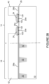
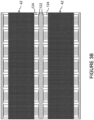
- Photoresist 42 is formed over the structure and patterned to remove portions of the photoresist 42, such that the remaining photoresist 42 covers the logic device region 16, but only portions of the memory cell region 14. Specifically, photoresist 42 covers front edges 120 and only a portion of each side edge 124. However, left uncovered by photoresist 42 are back edges 122 and a portion of each side edge 124, including the portions of oxide layer 26c thereon, as shown in Figs. 2B and 3B .
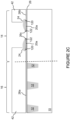
- oxide etch (e.g., wet or dry etch) is then performed on the exposed portions of oxide layer 26c and oxide 24, which reduces the thickness of layer portion 26c on portions of the side edges 124 and on back edges 122 (which are not subjected to high voltage operation), as shown in Fig. 2C .
- the photoresist 42 protects oxide layer portion 26a in the logic device region 16, as well as the oxide layer portions 26b on the substrate surface that are adjacent front edges 120 (on which the control gates will eventually be formed) and the other portions of oxide layer 26c.
- Control gates 28a in each row are formed as a continuous word line WL.
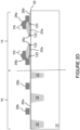
- Each control gate 28a extends up and over a respective front edge 120, and over a portion of each respective side edge 124, including a tunnel region portion TR of each side edge 124 for which layer portion 26c was thinned by the oxide etch shown in Fig. 2C and is now vertically covered by control gate 28a.
- the resulting structure has logic gates 28b and control gates 28a insulated from the substrate 10 by portions of the oxide layer 26 (i.e., oxide portions 26a and 26b) having a first thickness, and the control gates 28a are insulated from the tunnel region portion TR of the side edges 124 by the thinned portions of oxide 26c having a second thickness that is less than the first thickness.
- This structure enhances the erase efficiency and performance of the memory cell by enhancing tunneling efficiency between the control gate 28a and the tunnel region portions TR of the side edges 124, without compromising the performance of the logic devices or adversely affecting the ability of the control gates 28a to control the conductivity of the channel region portion of the substrate underneath the control gates 28a.
- the above described technique thins the oxide layer 26c on the tunnel region portions TR of the side edges 124 without risk of compromising the oxide layer portions 26a and 26b on which the logic gates 28b and control gate 28a are formed and which insulate them from the substrate 10.
- Fig. 5 illustrates an alternate embodiment, which is the same as the embodiment shown in Fig. 3C , except notches 44 are formed in the word lines WL at center portions of the floating gate 20a resulting in protruding tabs 46 of the control gates 28a extending out further over the side edges 124 than over the center of the floating gate 20a (i.e., each control gate 28a extends deeper over portions of side edges 124 than over a center portion of the floating gate 20a relative to front edge 120, such that the control gate 28a does not extend vertically over a portion of the floating gate 20a located between the tunnel region portion TR of the first side edge 124 and the tunnel region portion TR of the second side edge 124).
- Notch 44 reduces the amount of overlap between the control gate 28a and floating gate 20a (in the center area of the floating gate 20a that does not contribute to erasure), thus reducing capacitive coupling between control gate 28a and floating gate 20a which in turn can further enhance erase efficiency.
- Fig. 6 illustrates another alternate embodiment, which is the same as the embodiment shown in Fig. 5 , except that for each row of floating gates 20a, alternate tabs 46 are omitted, so that each control gate 28a extends over just one tunnel region portion TR of one side edge for each underlying floating gate 20a.
- the pattern of tabs 46 can alternate row by row, so tabs 46 in even numbered rows of floating gates 20a are disposed over different isolation regions 12 than tabs 46 in odd numbered rows of the floating gates 20a, as shown in Fig. 6 .
- Figs. 7A-7D illustrate yet another alternate embodiment, which starts with the structure shown in Fig. 2B .
- the oxide etch is performed to entirely remove the exposed oxide (i.e., a wet or dry oxide etch is performed on the exposed portions of oxide layer 26c and oxide 24, which removes the oxide layer portions 26c on the side edges 124 and on back edges 122 and removes exposed portions of oxide 24), as shown in Fig. 7A .
- the photoresist 42 protects oxide layer portion 26a in the logic device region 16, as well as the oxide layer portions 26b on the substrate surface that are adjacent front edges 120 (on which the control gates will eventually be formed) and the other portions of oxide layer 26c protected by photoresist 42.
- a layer of oxide 50 is then formed on the exposed portions of floating gates 20a and substrate 10 (e.g., by thermal oxidation), as shown in Fig. 7B .
- the thickness of layer 50 can be optimized for a tunnel oxide and is less than the thickness of the remaining oxide layer portions 26a, 26b and 26c. Formation of oxide 50 can be performed simultaneously in the logic device region 16 for forming logic devices suitable for low voltage operation.
- the structure is processed as described above with respect to Fig. 2D to form the logic gates 28b and control gates 28a, as shown in Fig. 7C .
- This structure is then processed as described above with respect to Fig. 2E to form the various source and drain regions, as shown in Fig. 7D .
- This embodiment can be utilized to form any of the configurations in Figs. 3C , 5 and 6 .
- the advantage of this embodiment is that the thickness of oxide layer 50 may be better controlled relative to the thickness of thinned portions of oxide layer 26c.
- the term “adjacent” includes “directly adjacent” (no intermediate materials, elements or space disposed there between) and “indirectly adjacent” (intermediate materials, elements or space disposed there between), “mounted to” includes “directly mounted to” (no intermediate materials, elements or space disposed there between) and “indirectly mounted to” (intermediate materials, elements or spaced disposed there between), and “electrically coupled” includes “directly electrically coupled to” (no intermediate materials or elements there between that electrically connect the elements together) and “indirectly electrically coupled to” (intermediate materials or elements there between that electrically connect the elements together).
- forming an element "over a substrate” can include forming the element directly on the substrate with no intermediate materials/elements there between, as well as forming the element indirectly on the substrate with one or more intermediate materials/elements there between.
Landscapes
- Engineering & Computer Science (AREA)
- Manufacturing & Machinery (AREA)
- Non-Volatile Memory (AREA)
- Semiconductor Memories (AREA)
Description
- The present invention relates to split-gate non-volatile memory cells, and more particularly to a method of forming such cells.
- Split-gate type memory cell arrays are known. For example,
U.S. Patent 5,029,130 , which is incorporated herein by reference for all purposes, discloses a split gate memory cell and its formation, which includes forming source and drain regions in the substrate with a channel region there between. A floating gate is disposed over and controls the conductivity of one portion of the channel region, and a control gate is disposed over and controls the conductivity of the other portion of the channel region. The control gate extends up and over the floating gate. The insulation between the floating gate and the control gate is referred to as the tunnel dielectric material (e.g. silicon dioxide, also referred to as oxide), because electrons tunnel through this dielectric material during an erase operation. -
US 20080050875 A1 discloses that a method of fabricating a compound device includes forming a first gate insulating pattern on a semiconductor substrate including a first region and a second region, forming a second gate insulating layer on the first gate insulating pattern, and after forming the second gate insulating layer, forming a well in the second region of the semiconductor substrate. - It is also known to form high voltage logic devices on the same wafer (substrate) as the split-gate memory cell array.
Figures 1A-1G show the steps in forming high voltage logic devices (e.g. 12 volt logic devices) on the same wafer as the split gate memory cells according to a conventional method. Asilicon semiconductor substrate 10 having anupper surface 10a, amemory cell region 14 and alogic region 16.Semiconductor substrate 10 is masked, i.e. photo resist is deposited, selectively exposed using a mask, and patterned (i.e., portions selectively removed) using a photolithographic process, leaving portions of the underlying material covered by remaining photo resist while leaving other portions of the underlying material (here thesilicon semiconductor substrate 10, particularlyupper surface 10a) exposed. The exposed substrate portions are etched away leaving trenches that are then filled with dielectric material (e.g. oxide) to formisolation regions 12 in thelogic region 16 of the wafer, as shown inFig. 1A (after photoresist removal).Isolation regions 12 are similarly formed inmemory cell region 14 of the wafer (not shown), defining alternating columns ofactive regions 13 andisolation regions 12. - A dielectric material (e.g. silicon dioxide, hereinafter referred to as oxide) 18 is formed on the
substrate 10, a layer of polysilicon (hereinafter referred to as poly) 20 is formed onoxide layer 18, and a layer of silicon nitride (hereinafter referred to as nitride) 22 is formed onpoly layer 20, as shown inFig. 1B . The wafer is masked with photoresist, and thenitride layer 22 selectively etched through openings in the photoresist in thememory cell region 14, to expose portions of theunderlying poly layer 20. The exposed portions of thepoly layer 20 are oxidized using an oxidation process, formingoxide areas 24 on thepoly layer 20, as shown inFig. 1C (after photoresist removal). - A nitride etch is used to remove the
remaining nitride layer 22. An anisotropic poly etch is used to remove exposed portions of thepoly layer 20, leavingblocks 20a ofpoly layer 20 underneath theoxide areas 24 in the memory cell region 14 (poly blocks 20a will constitute the floating gates of the memory cells), as shown inFig. 1D . An oxide etch is used to remove the exposed portions of oxide layer 18 (i.e., those portions not under the remaining portion of poly layer 20). Anoxide layer 26 is then formed over the structure either by deposition (which also thickens oxide areas 24) and/or by oxidation (which has no effect on oxide areas 24), as shown inFig. 1E . A poly layer is then formed on the structure (i.e., onoxide layer 26 and oxide areas 24). The poly layer is then patterned by forming and patterning photoresist on the poly layer leaving portions of the poly layer exposed. The exposed portions of the poly layer are selectively removed by a poly etch, leavingpoly blocks 28a in the memory cell region andpoly blocks 28b in the logic region, as shown inFig. 1F (after photoresist removal).Insulation spacers 30 are formed on the sides ofpoly blocks source regions 32 anddrain regions 34 in thememory cell region 14, andsource regions 36 anddrain regions 38 in thelogic region 16, ofsubstrate 10. The final structure is shown inFig. 1G . - The above technique produces non-volatile memory cells (each with a
floating gate 20a formed from the remaining portion ofpoly layer 20, a control gate in the form ofpoly block 28a, asource region 32 adjacent to (and also preferably extending partially under) an end of thefloating gate 20a, and adrain region 34 adjacent an end of thecontrol gate 28a) on thesame substrate 10 as high voltage logic devices (each with a logic gate in the form ofpoly block 28b,source region 36 anddrain region 38 adjacent first and second ends of thelogic gate 28b). There are many advantages of this technique. First, the same poly layer is used to form bothcontrol gates 28a of the memory cells and thelogic gates 28b of the logic devices, using a single poly deposition. Second, thesame oxide layer 26 is used as the gate oxide for the logic devices (i.e., the oxide layer used to insulate thelogic gates 28b from the substrate 10), the word line oxide for the memory cells (i.e., the oxide layer used to insulate thecontrol gates 28a from the substrate 10), and the tunnel oxide for the memory cells (i.e., the oxide insulating thefloating gate 20a from thecontrol gate 28a through which electrons tunnel in the erase operation). Common manufacturing steps for forming elements in both thememory cell region 14 and thelogic region 16 simplifies, expedites and lower the costs of manufacturing. Formingoxide areas 24, as described in relation toFig. 1E , by oxidation results in thefloating gates 20a having a concave upper surface that terminates in asharp edge 120 facing thecontrol gate 28a, which enhances tunneling performance and efficiency during erase (i.e., the erase operation includes placing a high voltage on thecontrol gate 28a to cause electrons to tunnel from thesharp edge 120 of thefloating gate 20a, throughoxide layer 26, to thecontrol gate 28a). Thecontrol gate 28a has a lower portion vertically over and insulated from thesubstrate 10 for controlling the conductivity of the channel region therein, and a second portion that extends up and over thefloating gate 20a for voltage coupling and proximity to the floating gatesharp edge 120 for erasure. - One drawback of the above described technique is that the thickness of
oxide layer 26 must be compatible for both the logic devices and the memory cells. Specifically, theoxide layer 26 must be thick enough for the high voltage operation of thelogic gates 28b andcontrol gates 28a, while being thin enough to allow tunneling from thefloating gate 20a to thecontrol gate 28a during the erase operation. Therefore, balancing these considerations, there is a lower limit to the thickness ofoxide layer 26 driven by the high voltage operation of thecontrol gates 28a andlogic gates 28b, which means the portion oflayer 26 through which tunneling occurs during erase operations of the memory cells (i.e. the portion oflayer 26 between thecontrol gate 28a and floatinggate 20a) is unnecessarily thick and therefore limits erase performance and efficiency, and limits endurance performance. However, forming the tunnel oxide (between thecontrol gate 28a and floatinggate 20a) separately from the word line oxide (between thecontrol gate 28a and the substrate 10) and the logic gate oxide (between thelogic gate 28b and the substrate 10) can significantly increase manufacturing complexity, time and costs, as well as risk the integrity of the previously formed word line oxide and logic gate oxide thus lowering yield. - It would be desirable to increase memory cell erase efficiency between the floating gate and the control gate, without adversely affecting the performance of the control gate as a word line or of the logic gate in the logic device, where the same oxide layer is used in all three places.
- The present invention is defined in the independent claims. Preferred embodiments are defined in the dependent claims. The aforementioned problems and needs are addressed by providing a memory device that includes a substrate of semiconductor material with a substrate upper surface having a memory cell region and a logic region, a floating gate disposed vertically over and insulated from the memory cell region of the substrate upper surface wherein the floating gate includes an upper surface that terminates in opposing front and back edges and in opposing first and second side edges, an oxide layer having a first portion that extends along the logic region of the substrate upper surface and has a first thickness a second portion that extends along the memory cell region of the substrate upper surface and has the first thickness and a third portion that extends along the front and back edges and along the first and second side edges, wherein the third portion of the oxide layer extending along the front edge has the first thickness and wherein the third portion of the oxide layer extending along a tunnel region portion of the first side edge has a second thickness less than the first thickness, a control gate having a first portion disposed on the second portion of the oxide layer and having a second portion disposed vertically over the front edge and vertically over the tunnel region portion of the first side edge, and a logic gate on the first portion of the oxide layer. The first portion of the oxide layer insulates the substrate from the logic gate, the second portion of the oxide layer insulates the substrate from the control gate first portion, and the third portion of the oxide layer along the tunnel region portion of the first side edge insulates the control gate second portion from the tunnel region portion of the first side edge.
- A method of forming a memory device includes providing a substrate of semiconductor material with a substrate upper surface having a memory cell region and a logic region, forming a floating gate disposed vertically over and insulated from the memory cell region of the substrate upper surface wherein the floating gate includes an upper surface that terminates in opposing front and back edges and in opposing first and second side edges, forming an oxide layer having a first portion that extends along the logic region of the substrate upper surface and a second portion that extends along the memory cell region of the substrate upper surface and a third portion that extends along the front and back edges and along the first and second side edges, performing an oxide etch that reduces a thickness of the third portion of the oxide layer along a tunnel region portion of the first side edge wherein the first and second portions of the oxide layer and the third portion of the oxide layer along the front edge of the floating gate are protected from the oxide etch, forming a control gate having a first portion disposed on the second portion of the oxide layer and having a second portion disposed vertically over the front edge and vertically over the tunnel region portion of the first side edge, and forming a logic gate on the first portion of the oxide layer. The first portion of the oxide layer insulates the substrate from the logic gate and has a first thickness, the second portion of the oxide layer insulates the substrate from the control gate first portion and has the first thickness, and the third portion of the oxide layer along the tunnel region portion of the first side edge insulates the control gate second portion from the tunnel region portion of the first side edge and has a second thickness less than the first thickness.
- A memory device includes a substrate of semiconductor material with a substrate upper surface having a memory cell region and a logic region, a floating gate disposed vertically over and insulated from the memory cell region of the substrate upper surface wherein the floating gate includes an upper surface that terminates in opposing front and back edges and in opposing first and second side edges, a first oxide layer having a first portion that extends along the logic region of the substrate upper surface and has a first thickness and a second portion that extends along the memory cell region of the substrate upper surface and has the first thickness and a third portion that extends along the front edge and has the first thickness, a second oxide layer extending along a tunnel region portion of the first side edge and has a second thickness less than the first thickness, a control gate having a first portion disposed on the second portion of the oxide layer and having a second portion disposed vertically over the front edge and vertically over the tunnel region portion of the first side edge, and a logic gate on the first portion of the oxide layer. The first portion of the first oxide layer insulates the substrate from the logic gate, the second portion of the first oxide layer insulates the substrate from the control gate first portion, and the second oxide layer along the tunnel region portion of the first side edge insulates the control gate second portion from the tunnel region portion of the first side edge.
- A method of forming a memory device includes providing a substrate of semiconductor material with a substrate upper surface having a memory cell region and a logic region, forming a floating gate disposed vertically over and insulated from the memory cell region of the substrate upper surface wherein the floating gate includes an upper surface that terminates in opposing front and back edges and in opposing first and second side edges, forming a first oxide layer having a first portion that extends along the logic region of the substrate upper surface and a second portion that extends along the memory cell region of the substrate upper surface and a third portion that extends along the front and back edges and along the first and second side edges, performing an oxide etch that removes the third portion of the first oxide layer along a tunnel region portion of the first side edge wherein the first and second portions of the first oxide layer and the third portion of the first oxide layer along the front edge of the floating gate are protected from the oxide etch, forming a second oxide layer along the tunnel region portion of the first side edge, forming a control gate having a first portion disposed on the second portion of the first oxide layer and having a second portion disposed vertically over the front edge and vertically over the tunnel region portion of the first side edge, and forming a logic gate on the first portion of the first oxide layer. The first portion of the first oxide layer insulates the substrate from the logic gate and has a first thickness, the second portion of the first oxide layer insulates the substrate from the control gate first portion and has the first thickness, and the second oxide layer along the tunnel region portion of the first side edge insulates the control gate second portion from the tunnel region portion of the first side edge and has a second thickness less than the first thickness.
- Other objects and features of the present invention will become apparent by a review of the specification, claims and appended figures.
-
-
Figs. 1A-1G are side cross-sectional views illustrating conventional steps for forming memory cells and logic devices on a common substrate. -
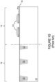
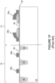
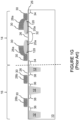
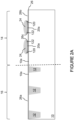
Figs. 2A-2E are side cross-sectional views illustrating steps for forming memory cells and logic devices on a common substrate in accordance with the present invention. -
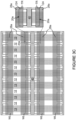
Figs. 3A-3C are top views illustrating steps for forming memory cells and logic devices on a common substrate in accordance with the present invention. -
Fig. 4 is a side cross-sectional view illustrating an implantation. -
Fig. 5 is a top view illustrating an alternate embodiment of the present invention. -
Fig. 6 is a top view illustrating an alternate embodiment of the present invention. -
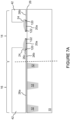
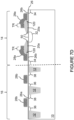
Figs. 7A-7D are side cross-sectional views illustrating steps for forming memory cells and logic devices on a common substrate in accordance with an alternate embodiment of the present invention. - The present invention is a technique of forming memory cells and logic devices on a common substrate, where a portion of the oxide layer used as a tunnel oxide is selectively thinned.
-
Figs. 2A-2E and3A-3C disclose steps of an embodiment of the method of the present invention. The process begins using the same steps described above with respect toFigs. 1A-1E , resulting in the structure shown in the cross sectional view of thememory cell region 14 andlogic device region 16 inFig. 2A , and shown in the top view of thememory cell region 14 inFig. 3A . At this stage of processing, there are alternating columns ofactive regions 13 andisolation regions 12 in thememory cell region 14, with pairs of floatinggates 20a formed in eachactive region column 13. Each floatinggate 20a has a concave upper surface terminating insharp edges gate 20a. Each floatinggate 20a partially overlap therespective isolation region 12 to provide margin for any misalignment. Specifically, for each pair of floatinggates 20a,sharp edges 120 are the two edges of the two floatinggates 20a that face away from each other (also referred to as front edges 120),sharp edges 122 are the two edges of the two floatinggates 20a that face toward each other (also referred to as back edges 122), andsharp edges 124 are the two edges of each floatinggate 20a extending betweensharp edges gate 20a, front andback edges side edges 124 oppose each other (also referred to as first and second side edges 124). Floatinggates 20a are shown and described herein as rectangular, but they need not be rectangular in shape. Sourceline diffusion areas 40 each extend in the row direction and between the pairs of the floatinggates 20a (for connecting together a row of the source regions formed later in the process).Oxide layer 26 can be considered to have three portions: afirst portion 26a that extends along thelogic region 16 of the substrateupper surface 10a, asecond portion 26b that extends along thememory cell region 14 of the substrateupper surface 10a, and athird portion 26c that extends along the sides andsharp edges gates 20a. -
Photoresist 42 is formed over the structure and patterned to remove portions of thephotoresist 42, such that the remainingphotoresist 42 covers thelogic device region 16, but only portions of thememory cell region 14. Specifically,photoresist 42 coversfront edges 120 and only a portion of eachside edge 124. However, left uncovered byphotoresist 42 are backedges 122 and a portion of eachside edge 124, including the portions ofoxide layer 26c thereon, as shown inFigs. 2B and3B . - An oxide etch (e.g., wet or dry etch) is then performed on the exposed portions of
oxide layer 26c andoxide 24, which reduces the thickness oflayer portion 26c on portions of the side edges 124 and on back edges 122 (which are not subjected to high voltage operation), as shown inFig. 2C . Thephotoresist 42 protectsoxide layer portion 26a in thelogic device region 16, as well as theoxide layer portions 26b on the substrate surface that are adjacent front edges 120 (on which the control gates will eventually be formed) and the other portions ofoxide layer 26c. - After
photoresist 42 is removed, a poly layer deposition and patterning as described above with respect toFigs. 1E - 1F is performed to form the control gates formed frompoly blocks 28a and logic gates formed frompoly blocks 28b, as shown inFig. 2D and3C .Control gates 28a in each row are formed as a continuous word line WL. Eachcontrol gate 28a extends up and over a respectivefront edge 120, and over a portion of eachrespective side edge 124, including a tunnel region portion TR of eachside edge 124 for whichlayer portion 26c was thinned by the oxide etch shown inFig. 2C and is now vertically covered bycontrol gate 28a. Specifically, the tunnel region portion TR is that portion of eachside edge 124 which was subjected tooxide layer 26a thinning and which is later vertically covered bycontrol gate 28a. The remaining steps described above with respect toFig. 1F are performed to result in the final structure shown inFig. 2E . Preferably a single implantation is used to simultaneously form thedrain regions 34 in thememory cell region 14, andsource regions 36 anddrain regions 38 in thelogic region 16, as shown inFig. 4 . - The resulting structure has
logic gates 28b andcontrol gates 28a insulated from thesubstrate 10 by portions of the oxide layer 26 (i.e.,oxide portions control gates 28a are insulated from the tunnel region portion TR of the side edges 124 by the thinned portions ofoxide 26c having a second thickness that is less than the first thickness. This structure enhances the erase efficiency and performance of the memory cell by enhancing tunneling efficiency between thecontrol gate 28a and the tunnel region portions TR of the side edges 124, without compromising the performance of the logic devices or adversely affecting the ability of thecontrol gates 28a to control the conductivity of the channel region portion of the substrate underneath thecontrol gates 28a. Specifically, the above described technique thins theoxide layer 26c on the tunnel region portions TR of the side edges 124 without risk of compromising theoxide layer portions logic gates 28b and controlgate 28a are formed and which insulate them from thesubstrate 10. -
Fig. 5 illustrates an alternate embodiment, which is the same as the embodiment shown inFig. 3C , exceptnotches 44 are formed in the word lines WL at center portions of the floatinggate 20a resulting in protrudingtabs 46 of thecontrol gates 28a extending out further over the side edges 124 than over the center of the floatinggate 20a (i.e., eachcontrol gate 28a extends deeper over portions of side edges 124 than over a center portion of the floatinggate 20a relative tofront edge 120, such that thecontrol gate 28a does not extend vertically over a portion of the floatinggate 20a located between the tunnel region portion TR of thefirst side edge 124 and the tunnel region portion TR of the second side edge 124).Notch 44 reduces the amount of overlap between thecontrol gate 28a and floatinggate 20a (in the center area of the floatinggate 20a that does not contribute to erasure), thus reducing capacitive coupling betweencontrol gate 28a and floatinggate 20a which in turn can further enhance erase efficiency. -
Fig. 6 illustrates another alternate embodiment, which is the same as the embodiment shown inFig. 5 , except that for each row of floatinggates 20a,alternate tabs 46 are omitted, so that eachcontrol gate 28a extends over just one tunnel region portion TR of one side edge for each underlying floatinggate 20a. The pattern oftabs 46 can alternate row by row, sotabs 46 in even numbered rows of floatinggates 20a are disposed overdifferent isolation regions 12 thantabs 46 in odd numbered rows of the floatinggates 20a, as shown inFig. 6 . -
Figs. 7A-7D illustrate yet another alternate embodiment, which starts with the structure shown inFig. 2B . However, unlike the results of the oxide etch shown inFig. 2C where the exposed portions ofoxide layer 26c are maintained but reduced in thickness, the oxide etch is performed to entirely remove the exposed oxide (i.e., a wet or dry oxide etch is performed on the exposed portions ofoxide layer 26c andoxide 24, which removes theoxide layer portions 26c on the side edges 124 and onback edges 122 and removes exposed portions of oxide 24), as shown inFig. 7A . Thephotoresist 42 protectsoxide layer portion 26a in thelogic device region 16, as well as theoxide layer portions 26b on the substrate surface that are adjacent front edges 120 (on which the control gates will eventually be formed) and the other portions ofoxide layer 26c protected byphotoresist 42. - A layer of
oxide 50 is then formed on the exposed portions of floatinggates 20a and substrate 10 (e.g., by thermal oxidation), as shown inFig. 7B . The thickness oflayer 50 can be optimized for a tunnel oxide and is less than the thickness of the remainingoxide layer portions oxide 50 can be performed simultaneously in thelogic device region 16 for forming logic devices suitable for low voltage operation. Afterphotoresist 42 removed, the structure is processed as described above with respect toFig. 2D to form thelogic gates 28b andcontrol gates 28a, as shown inFig. 7C . This structure is then processed as described above with respect toFig. 2E to form the various source and drain regions, as shown inFig. 7D . This embodiment can be utilized to form any of the configurations inFigs. 3C ,5 and6 . The advantage of this embodiment is that the thickness ofoxide layer 50 may be better controlled relative to the thickness of thinned portions ofoxide layer 26c. - It is to be understood that the present invention is not limited to the embodiment(s) described above and illustrated herein, but encompasses any and all variations falling within the scope of the appended claims. For example, references to the present invention herein are not intended to limit the scope of any claim or claim term, but instead merely make reference to one or more features that may be covered by one or more of the claims. Materials, processes and numerical examples described above are exemplary only, and should not be deemed to limit the claims. Further, as is apparent from the claims and specification, not all method steps need be performed in the exact order illustrated or claimed.
- It should be noted that, as used herein, the terms "over" and "on" both inclusively include "directly on" (no intermediate materials, elements or space disposed there between) and "indirectly on" (intermediate materials, elements or space disposed there between). Likewise, the term "adjacent" includes "directly adjacent" (no intermediate materials, elements or space disposed there between) and "indirectly adjacent" (intermediate materials, elements or space disposed there between), "mounted to" includes "directly mounted to" (no intermediate materials, elements or space disposed there between) and "indirectly mounted to" (intermediate materials, elements or spaced disposed there between), and "electrically coupled" includes "directly electrically coupled to" (no intermediate materials or elements there between that electrically connect the elements together) and "indirectly electrically coupled to" (intermediate materials or elements there between that electrically connect the elements together). For example, forming an element "over a substrate" can include forming the element directly on the substrate with no intermediate materials/elements there between, as well as forming the element indirectly on the substrate with one or more intermediate materials/elements there between.
Claims (15)
- A memory device, comprising:a substrate of semiconductor material (10) with a substrate upper surface (10a) having a memory cell region (14) and a logic region (16);a floating gate (20a) disposed vertically over and insulated from the memory cell region of the substrate upper surface, wherein the floating gate includes an upper surface that terminates in opposing front and back edges and in opposing first and second side edges;an oxide layer (26) having a first portion that extends on the logic region of the substrate upper surface and has a first thickness, a second portion that extends on the memory cell region of the substrate upper surface and has the first thickness, and a third portion that extends on the front and back edges and on the first and second side edges;wherein the third portion of the oxide layer extending on the front edge has the first thickness, and wherein the third portion of the oxide layer extending on a tunnel region portion (TR) of the first side edge has a second thickness less than the first thickness;a control gate (28a) having a first portion disposed on the second portion of the oxide layer, and having a second portion disposed vertically over the front edge and vertically over the tunnel region portion of the first side edge; anda logic gate (28b) on the first portion of the oxide layer;wherein the first portion of the oxide layer insulates the substrate from the logic gate, the second portion of the oxide layer insulates the substrate from the control gate first portion, and the third portion of the oxide layer on the tunnel region portion of the first side edge insulates the control gate second portion from the tunnel region portion of the first side edge, the lesser thickness of the third portion of the oxide layer on the tunnel region portion of the first side edge enhancing the tunneling efficiency between the second portion of the control gate and the tunnel region portion of the first side edge.
- The device of claim 1, wherein:the third portion of the oxide layer extending on a tunnel region portion of the second side edge has the second thickness;the control gate second portion is further disposed vertically over the tunnel region portion of the second side edge; andthe third portion of the oxide layer on the tunnel region portion of the second side edge insulates the control gate second portion from the tunnel region portion of the second side edge.
- A method of forming a memory device, comprising:providing a substrate of semiconductor material (10) with a substrate upper surface (10a) having a memory cell region and a logic region;forming a floating gate (20a) disposed vertically over and insulated from the memory cell region of the substrate upper surface, wherein the floating gate includes an upper surface that terminates in opposing front and back edges and in opposing first and second side edges;forming an oxide layer (26) having a first portion that extends on the logic region of the substrate upper surface, a second portion that extends on the memory cell region of the substrate upper surface, and a third portion that extends on the front and back edges and on the first and second side edges;performing an oxide etch that reduces a thickness of the third portion of the oxide layer on a tunnel region portion (TR) of the first side edge, wherein the first and second portions of the oxide layer and the third portion of the oxide layer on the front edge of the floating gate are protected from the oxide etch;forming a control gate (28a) having a first portion disposed on the second portion of the oxide layer, and having a second portion disposed vertically over the front edge and vertically over the tunnel region portion of the first side edge; andforming a logic gate (28b) on the first portion of the oxide layer;wherein the first portion of the oxide layer insulates the substrate from the logic gate and has a first thickness, the second portion of the oxide layer insulates the substrate from the control gate first portion and has the first thickness, and the third portion of the oxide layer on the tunnel region portion of the first side edge insulates the control gate second portion from the tunnel region portion of the first side edge and has a second thickness less than the first thickness, the lesser thickness of the third portion of the oxide layer on the tunnel region portion of the first side edge enhancing the tunneling efficiency between the second portion of the control gate and the tunnel region portion of the first side edge.
- The method of claim 3, wherein the forming of the control gate and the forming of the logic gate comprise:forming a polysilicon layer on the first, second and third portions of the oxide layer; andselectively removing portions of the polysilicon layer leaving a first portion of the polysilicon layer as the formed control gate and leaving a second portion of the polysilicon layer as the formed logic gate.
- The method of claim 3, wherein:the performing of the oxide etch further comprises reducing a thickness of the third portion of the oxide layer on a tunnel region portion of the second side edge;the control gate second portion is disposed vertically over the tunnel region portion of the second side edge; andthe third portion of the oxide layer on the tunnel region portion of the second side edge insulates the control gate second portion from the tunnel region portion of the second side edge and has the second thickness.
- A memory device, comprising:a substrate of semiconductor material (10) with a substrate upper surface (10a) having a memory cell region (14) and a logic region (16);a floating gate (20a) disposed vertically over and insulated from the memory cell region of the substrate upper surface, wherein the floating gate includes an upper surface that terminates in opposing front and back edges and in opposing first and second side edges;a first oxide layer (26) having a first portion that extends on the logic region of the substrate upper surface and has a first thickness, a second portion that extends on the memory cell region of the substrate upper surface and has the first thickness, and a third portion that extends on the front edge and has the first thickness;a second oxide layer (50) extending on a tunnel region portion (TR) of the first side edge and has a second thickness less than the first thickness;a control gate (28a) having a first portion disposed on the second portion of the oxide layer, and having a second portion disposed vertically over the front edge and vertically over the tunnel region portion of the first side edge; anda logic gate (28b) on the first portion of the oxide layer;wherein the first portion of the first oxide layer insulates the substrate from the logic gate, the second portion of the first oxide layer insulates the substrate from the control gate first portion, and the second oxide layer on the tunnel region portion of the first side edge insulates the control gate second portion from the tunnel region portion of the first side edge, the lesser thickness of the second oxide layer enhancing the tunneling efficiency between the second portion of the control gate and the tunnel region portion of the first side edge.
- The device of claim 1 or claim 6, wherein the upper surface of the floating gate is concave such that the front and back edges and the first and second side edges are sharp edges.
- The device of claim 1 or claim 6, further comprising:a first source region in the substrate adjacent an end of the floating gate;a first drain region in the substrate adjacent an end of the control gate;a second source region in the substrate adjacent a first end of the logic gate; anda second drain region in the substrate adjacent a second end of the logic gate.
- The device of claim 6, wherein:the second oxide layer further extends on a tunnel region portion of the second side edge and has the second thickness;the control gate second portion is further disposed vertically over the tunnel region portion of the second side edge; andthe second oxide layer on the tunnel region portion of the second side edge insulates the control gate second portion from the tunnel region portion of the second side edge.
- A method of forming a memory device, comprising:providing a substrate of semiconductor material (10) with a substrate upper surface (10a) having a memory cell region (14) and a logic region (16);forming a floating gate (20a) disposed vertically over and insulated from the memory cell region of the substrate upper surface, wherein the floating gate includes an upper surface that terminates in opposing front and back edges and in opposing first and second side edges;forming a first oxide (26) layer having a first portion that extends on the logic region of the substrate upper surface, a second portion that extends on the memory cell region of the substrate upper surface, and a third portion that extends on the front and back edges and on the first and second side edges;performing an oxide etch that removes the third portion of the first oxide layer on a tunnel region portion of the first side edge, wherein the first and second portions of the first oxide layer and the third portion of the first oxide layer on the front edge of the floating gate are protected from the oxide etch;forming a second oxide layer (50) on the tunnel region portion (TR) of the first side edge;forming a control gate (28a) having a first portion disposed on the second portion of the first oxide layer, and having a second portion disposed vertically over the front edge and vertically over the tunnel region portion of the first side edge; andforming a logic gate (28b) on the first portion of the first oxide layer;wherein the first portion of the first oxide layer insulates the substrate from the logic gate and has a first thickness, the second portion of the first oxide layer insulates the substrate from the control gate first portion and has the first thickness, and the second oxide layer on the tunnel region portion of the first side edge insulates the control gate second portion from the tunnel region portion of the first side edge and has a second thickness less than the first thickness, the lesser thickness of the second oxide layer enhancing the tunneling efficiency between the second portion of the control gate and the tunnel region portion of the first side edge.
- The method of claim 3 or claim 10, further comprising:
oxidizing the upper surface of the floating gate so that the upper surface of the floating gate is concave, and so that the front and back edges and the first and second side edges are sharp edges. - The method of claim 10, wherein the forming of the control gate and the forming of the logic gate comprise:forming a polysilicon layer on the first, second and third portions of the first oxide layer and on the second oxide layer; andselectively removing portions of the polysilicon layer leaving a first portion of the polysilicon layer as the formed control gate and leaving a second portion of the polysilicon layer as the formed logic gate.
- The method of claim 3 or claim 10, further comprising:forming a first source region in the substrate adjacent an end of the floating gate;forming a first drain region in the substrate adjacent an end of the control gate;forming a second source region in the substrate adjacent a first end of the logic gate; andforming a second drain region in the substrate adjacent a second end of the logic gate;wherein the forming of the first drain region, the second source region and the second drain region are performed simultaneously by an implantation process.
- The method of claim 10, wherein:the forming of the second oxide layer further comprises forming the second oxide layer on a tunnel region portion of the second side edge;the control gate second portion is disposed vertically over the tunnel region portion of the second side edge; andthe second oxide layer on the tunnel region portion of the second side edge insulates the control gate second portion from the tunnel region portion of the second side edge and has the second thickness.
- The device of claim 2 or claim 9, or the method of claim 5 or claim 14,
wherein the second portion of the control gate extends vertically over a portion of the floating gate between the tunnel region portion of the first side edge and the tunnel region portion of the second side edge, or
wherein the second portion of the control gate does not extend vertically over a portion of the floating gate between the tunnel region portion of the first side edge and the tunnel region portion of the second side edge.
Applications Claiming Priority (2)
| Application Number | Priority Date | Filing Date | Title |
|---|---|---|---|
| US16/910,022 US11362218B2 (en) | 2020-06-23 | 2020-06-23 | Method of forming split gate memory cells with thinned side edge tunnel oxide |
| PCT/US2020/066451 WO2021262232A1 (en) | 2020-06-23 | 2020-12-21 | Method of forming split gate memory cells with thinned side edge tunnel oxide |
Publications (2)
| Publication Number | Publication Date |
|---|---|
| EP4169071A1 EP4169071A1 (en) | 2023-04-26 |
| EP4169071B1 true EP4169071B1 (en) | 2024-11-20 |
Family
ID=74187393
Family Applications (1)
| Application Number | Title | Priority Date | Filing Date |
|---|---|---|---|
| EP20842650.2A Active EP4169071B1 (en) | 2020-06-23 | 2020-12-21 | Method of forming split gate memory cells with thinned side edge tunnel oxide |
Country Status (7)
| Country | Link |
|---|---|
| US (1) | US11362218B2 (en) |
| EP (1) | EP4169071B1 (en) |
| JP (1) | JP7522869B2 (en) |
| KR (1) | KR102487234B1 (en) |
| CN (1) | CN116058093B (en) |
| TW (1) | TWI795783B (en) |
| WO (1) | WO2021262232A1 (en) |
Citations (2)
| Publication number | Priority date | Publication date | Assignee | Title |
|---|---|---|---|---|
| US7560765B2 (en) * | 2006-01-20 | 2009-07-14 | Samsung Electronics Co., Ltd. | Nonvolatile memory device and method of fabricating the same |
| US20160359024A1 (en) * | 2015-06-08 | 2016-12-08 | Silicon Storage Technology, Inc. | Method Of Forming Split Gate Memory Cells With 5 Volt Logic Devices |
Family Cites Families (37)
| Publication number | Priority date | Publication date | Assignee | Title |
|---|---|---|---|---|
| US5029130A (en) | 1990-01-22 | 1991-07-02 | Silicon Storage Technology, Inc. | Single transistor non-valatile electrically alterable semiconductor memory device |
| US5512505A (en) * | 1990-12-18 | 1996-04-30 | Sandisk Corporation | Method of making dense vertical programmable read only memory cell structure |
| US5889700A (en) * | 1997-05-05 | 1999-03-30 | National Semiconductor Corporation | High density EEPROM array using self-aligned control gate and floating gate for both access transistor and memory cell and method of operating same |
| JP3922341B2 (en) * | 2001-01-11 | 2007-05-30 | セイコーエプソン株式会社 | Manufacturing method of semiconductor device having nonvolatile memory transistor |
| US20030102504A1 (en) * | 2001-12-05 | 2003-06-05 | Geeng-Chuan Chern | Method of forming different oxide thickness for high voltage transistor and memory cell tunnel dielectric |
| US6828183B1 (en) * | 2002-04-11 | 2004-12-07 | Taiwan Semiconductor Manufacturing Company | Process for high voltage oxide and select gate poly for split-gate flash memory |
| US6902975B2 (en) | 2003-10-15 | 2005-06-07 | Taiwan Semiconductor Manufacturing Company, Ltd. | Non-volatile memory technology compatible with 1T-RAM process |
| US7241654B2 (en) * | 2003-12-17 | 2007-07-10 | Micron Technology, Inc. | Vertical NROM NAND flash memory array |
| US7816722B2 (en) * | 2004-02-04 | 2010-10-19 | Hewlett-Packard Development Company, L.P. | Memory array |
| JP4578938B2 (en) | 2004-11-08 | 2010-11-10 | 富士通セミコンダクター株式会社 | Semiconductor device |
| US7355240B2 (en) * | 2005-09-22 | 2008-04-08 | Taiwan Semiconductor Manufacturing Co., Ltd. | Semiconductor product including logic, non-volatile memory and volatile memory devices and method for fabrication thereof |
| KR100812237B1 (en) * | 2006-08-25 | 2008-03-10 | 삼성전자주식회사 | Manufacturing Method of Embedded Flash Memory Device |
| JP2009088060A (en) * | 2007-09-28 | 2009-04-23 | Nec Electronics Corp | Nonvolatile semiconductor memory device and manufacturing method thereof |
| JP2010004020A (en) | 2008-05-19 | 2010-01-07 | Toshiba Corp | Nonvolatile semiconductor memory device, and method for manufacturing the same |
| JP2011040626A (en) * | 2009-08-13 | 2011-02-24 | Renesas Electronics Corp | Semiconductor memory device and method for manufacturing semiconductor memory device |
| JP5613506B2 (en) | 2009-10-28 | 2014-10-22 | ルネサスエレクトロニクス株式会社 | Semiconductor device |
| JP5834909B2 (en) | 2011-12-28 | 2015-12-24 | 富士通セミコンダクター株式会社 | Manufacturing method of semiconductor device |
| US9111865B2 (en) * | 2012-10-26 | 2015-08-18 | Freescale Semiconductor, Inc. | Method of making a logic transistor and a non-volatile memory (NVM) cell |
| TWI534959B (en) * | 2014-02-11 | 2016-05-21 | 北京芯盈速騰電子科技有限責任公司 | Non-volatile memory and the manufacturing method thereof |
| TWI560810B (en) * | 2014-03-05 | 2016-12-01 | Xinova Technology Ltd | Non-volatile memory unit under the condition that low electric field source is erased and the manufacturing method thereof |
| US9343466B1 (en) * | 2014-12-29 | 2016-05-17 | Globalfoundries Singapore Pte. Ltd. | Methods for fabricating flash memory cells and integrated circuits having flash memory cells embedded with logic |
| KR101878114B1 (en) * | 2015-01-23 | 2018-07-12 | 실리콘 스토리지 테크놀로지 인크 | Method for forming self-aligned discrete gate memory cell arrays with metal gates and logic devices |
| US9728545B2 (en) * | 2015-04-16 | 2017-08-08 | Taiwan Semiconductor Manufacturing Co., Ltd. | Method for preventing floating gate variation |
| US9659948B2 (en) * | 2015-09-17 | 2017-05-23 | United Microelectronics Corp. | Semiconductor device and method of fabricating semiconductor device |
| US9634020B1 (en) * | 2015-10-07 | 2017-04-25 | Silicon Storage Technology, Inc. | Method of making embedded memory device with silicon-on-insulator substrate |
| US9972493B2 (en) * | 2016-08-08 | 2018-05-15 | Silicon Storage Technology, Inc. | Method of forming low height split gate memory cells |
| US10608090B2 (en) * | 2017-10-04 | 2020-03-31 | Silicon Storage Technology, Inc. | Method of manufacturing a split-gate flash memory cell with erase gate |
| JP7118616B2 (en) * | 2017-10-12 | 2022-08-16 | ラピスセミコンダクタ株式会社 | Semiconductor device and method for manufacturing semiconductor device |
| US10825914B2 (en) * | 2017-11-13 | 2020-11-03 | Taiwan Semiconductor Manufacturing Company, Ltd. | Manufacturing method of semiconductor device |
| US10468427B2 (en) * | 2018-01-23 | 2019-11-05 | Globalfoundries Singapore Pte. Ltd. | Poly-insulator-poly (PIP) capacitor |
| US10418451B1 (en) * | 2018-05-09 | 2019-09-17 | Silicon Storage Technology, Inc. | Split-gate flash memory cell with varying insulation gate oxides, and method of forming same |
| CN112185970B (en) * | 2019-07-02 | 2024-05-28 | 硅存储技术公司 | Method of forming a split gate memory cell |
| CN112185815B (en) * | 2019-07-04 | 2024-07-23 | 硅存储技术公司 | Method of forming a split gate flash memory cell |
| US11018147B1 (en) * | 2020-02-04 | 2021-05-25 | Silicon Storage Technology, Inc. | Method of forming split gate memory cells with thinned tunnel oxide |
| US11127752B2 (en) * | 2020-02-21 | 2021-09-21 | United Microelectronics Corp. | Structure of semiconductor device and method for fabricating the same |
| US11488970B2 (en) * | 2020-07-09 | 2022-11-01 | Silicon Storage Technology, Inc. | Method of forming split gate memory cells with thinner tunnel oxide |
| CN114256251B (en) * | 2020-09-21 | 2025-05-13 | 硅存储技术股份有限公司 | Method of forming a device having a memory cell, a high voltage device, and a logic device |
-
2020
- 2020-06-23 US US16/910,022 patent/US11362218B2/en active Active
- 2020-12-21 KR KR1020227038562A patent/KR102487234B1/en active Active
- 2020-12-21 EP EP20842650.2A patent/EP4169071B1/en active Active
- 2020-12-21 JP JP2022579031A patent/JP7522869B2/en active Active
- 2020-12-21 WO PCT/US2020/066451 patent/WO2021262232A1/en not_active Ceased
- 2020-12-21 CN CN202080102214.3A patent/CN116058093B/en active Active
-
2021
- 2021-05-21 TW TW110118430A patent/TWI795783B/en active
Patent Citations (2)
| Publication number | Priority date | Publication date | Assignee | Title |
|---|---|---|---|---|
| US7560765B2 (en) * | 2006-01-20 | 2009-07-14 | Samsung Electronics Co., Ltd. | Nonvolatile memory device and method of fabricating the same |
| US20160359024A1 (en) * | 2015-06-08 | 2016-12-08 | Silicon Storage Technology, Inc. | Method Of Forming Split Gate Memory Cells With 5 Volt Logic Devices |
Also Published As
| Publication number | Publication date |
|---|---|
| US11362218B2 (en) | 2022-06-14 |
| KR102487234B1 (en) | 2023-01-10 |
| TWI795783B (en) | 2023-03-11 |
| US20210399127A1 (en) | 2021-12-23 |
| CN116058093B (en) | 2024-02-13 |
| WO2021262232A1 (en) | 2021-12-30 |
| CN116058093A (en) | 2023-05-02 |
| EP4169071A1 (en) | 2023-04-26 |
| JP2023525396A (en) | 2023-06-15 |
| JP7522869B2 (en) | 2024-07-25 |
| TW202230725A (en) | 2022-08-01 |
| KR20220153113A (en) | 2022-11-17 |
Similar Documents
| Publication | Publication Date | Title |
|---|---|---|
| US6906379B2 (en) | Semiconductor memory array of floating gate memory cells with buried floating gate | |
| US6750090B2 (en) | Self aligned method of forming a semiconductor memory array of floating gate memory cells with floating gates having multiple sharp edges, and a memory array made thereby | |
| EP3248220B1 (en) | Method of forming split-gate memory cell array along with low and high voltage logic devices | |
| JP2021506113A (en) | Non-volatile split gate memory cell with integrated high K metal control gate and manufacturing method | |
| US20040207005A1 (en) | Nonvolatile memory cells having split gate structure and methods of fabricating the same | |
| EP3970188B1 (en) | Method of forming split gate memory cells | |
| US6967372B2 (en) | Semiconductor memory array of floating gate memory cells with vertical control gate sidewalls and insulation spacers | |
| TW202215440A (en) | Split-gate, 2-bit non-volatile memory cell with erase gate disposed over word line gate, and method of making same | |
| EP4101003B1 (en) | Method of forming split gate memory cells with thinned tunnel oxide | |
| EP3994731B1 (en) | Method of forming split-gate flash memory cell with spacer defined floating gate and discretely formed polysilicon gates | |
| EP2904631B1 (en) | Self-aligned method of forming a semiconductor memory array of floating gate memory cells with single poly layer | |
| US11362218B2 (en) | Method of forming split gate memory cells with thinned side edge tunnel oxide | |
| US20250344382A1 (en) | Semiconductor device and method with memory cells having coupling gate self-aligned to floating gate | |
| JP2001332638A (en) | Manufacturing method of semiconductor memory device |
Legal Events
| Date | Code | Title | Description |
|---|---|---|---|
| STAA | Information on the status of an ep patent application or granted ep patent |
Free format text: STATUS: UNKNOWN |
|
| STAA | Information on the status of an ep patent application or granted ep patent |
Free format text: STATUS: THE INTERNATIONAL PUBLICATION HAS BEEN MADE |
|
| PUAI | Public reference made under article 153(3) epc to a published international application that has entered the european phase |
Free format text: ORIGINAL CODE: 0009012 |
|
| STAA | Information on the status of an ep patent application or granted ep patent |
Free format text: STATUS: REQUEST FOR EXAMINATION WAS MADE |
|
| 17P | Request for examination filed |
Effective date: 20230110 |
|
| AK | Designated contracting states |
Kind code of ref document: A1 Designated state(s): AL AT BE BG CH CY CZ DE DK EE ES FI FR GB GR HR HU IE IS IT LI LT LU LV MC MK MT NL NO PL PT RO RS SE SI SK SM TR |
|
| DAV | Request for validation of the european patent (deleted) | ||
| DAX | Request for extension of the european patent (deleted) | ||
| REG | Reference to a national code |
Ref country code: DE Ref legal event code: R079 Free format text: PREVIOUS MAIN CLASS: H01L0027115360 Ipc: H01L0029423000 Ref country code: DE Ref legal event code: R079 Ref document number: 602020041805 Country of ref document: DE Free format text: PREVIOUS MAIN CLASS: H01L0027115360 Ipc: H01L0029423000 |
|
| RIC1 | Information provided on ipc code assigned before grant |
Ipc: H01L 21/28 20060101ALI20231130BHEP Ipc: H10B 41/49 20230101ALI20231130BHEP Ipc: H10B 41/44 20230101ALI20231130BHEP Ipc: H10B 41/10 20230101ALI20231130BHEP Ipc: H01L 29/423 20060101AFI20231130BHEP |
|
| GRAP | Despatch of communication of intention to grant a patent |
Free format text: ORIGINAL CODE: EPIDOSNIGR1 |
|
| STAA | Information on the status of an ep patent application or granted ep patent |
Free format text: STATUS: GRANT OF PATENT IS INTENDED |
|
| INTG | Intention to grant announced |
Effective date: 20240112 |
|
| GRAJ | Information related to disapproval of communication of intention to grant by the applicant or resumption of examination proceedings by the epo deleted |
Free format text: ORIGINAL CODE: EPIDOSDIGR1 |
|
| STAA | Information on the status of an ep patent application or granted ep patent |
Free format text: STATUS: REQUEST FOR EXAMINATION WAS MADE |
|
| INTC | Intention to grant announced (deleted) | ||
| P01 | Opt-out of the competence of the unified patent court (upc) registered |
Effective date: 20240416 |
|
| GRAP | Despatch of communication of intention to grant a patent |
Free format text: ORIGINAL CODE: EPIDOSNIGR1 |
|
| STAA | Information on the status of an ep patent application or granted ep patent |
Free format text: STATUS: GRANT OF PATENT IS INTENDED |
|
| INTG | Intention to grant announced |
Effective date: 20240612 |
|
| GRAS | Grant fee paid |
Free format text: ORIGINAL CODE: EPIDOSNIGR3 |
|
| GRAA | (expected) grant |
Free format text: ORIGINAL CODE: 0009210 |
|
| STAA | Information on the status of an ep patent application or granted ep patent |
Free format text: STATUS: THE PATENT HAS BEEN GRANTED |
|
| AK | Designated contracting states |
Kind code of ref document: B1 Designated state(s): AL AT BE BG CH CY CZ DE DK EE ES FI FR GB GR HR HU IE IS IT LI LT LU LV MC MK MT NL NO PL PT RO RS SE SI SK SM TR |
|
| REG | Reference to a national code |
Ref country code: GB Ref legal event code: FG4D |
|
| REG | Reference to a national code |
Ref country code: DE Ref legal event code: R079 Ref document number: 602020041805 Country of ref document: DE Free format text: PREVIOUS MAIN CLASS: H01L0029423000 Ipc: H10D0064270000 |
|
| REG | Reference to a national code |
Ref country code: CH Ref legal event code: EP |
|
| REG | Reference to a national code |
Ref country code: DE Ref legal event code: R096 Ref document number: 602020041805 Country of ref document: DE |
|
| REG | Reference to a national code |
Ref country code: IE Ref legal event code: FG4D |
|
| REG | Reference to a national code |
Ref country code: NL Ref legal event code: FP |
|
| REG | Reference to a national code |
Ref country code: LT Ref legal event code: MG9D |
|
| PG25 | Lapsed in a contracting state [announced via postgrant information from national office to epo] |
Ref country code: IS Free format text: LAPSE BECAUSE OF FAILURE TO SUBMIT A TRANSLATION OF THE DESCRIPTION OR TO PAY THE FEE WITHIN THE PRESCRIBED TIME-LIMIT Effective date: 20250320 Ref country code: PT Free format text: LAPSE BECAUSE OF FAILURE TO SUBMIT A TRANSLATION OF THE DESCRIPTION OR TO PAY THE FEE WITHIN THE PRESCRIBED TIME-LIMIT Effective date: 20250320 Ref country code: HR Free format text: LAPSE BECAUSE OF FAILURE TO SUBMIT A TRANSLATION OF THE DESCRIPTION OR TO PAY THE FEE WITHIN THE PRESCRIBED TIME-LIMIT Effective date: 20241120 |
|
| PG25 | Lapsed in a contracting state [announced via postgrant information from national office to epo] |
Ref country code: FI Free format text: LAPSE BECAUSE OF FAILURE TO SUBMIT A TRANSLATION OF THE DESCRIPTION OR TO PAY THE FEE WITHIN THE PRESCRIBED TIME-LIMIT Effective date: 20241120 |
|
| REG | Reference to a national code |
Ref country code: AT Ref legal event code: MK05 Ref document number: 1744404 Country of ref document: AT Kind code of ref document: T Effective date: 20241120 |
|
| PG25 | Lapsed in a contracting state [announced via postgrant information from national office to epo] |
Ref country code: BG Free format text: LAPSE BECAUSE OF FAILURE TO SUBMIT A TRANSLATION OF THE DESCRIPTION OR TO PAY THE FEE WITHIN THE PRESCRIBED TIME-LIMIT Effective date: 20241120 |
|
| PG25 | Lapsed in a contracting state [announced via postgrant information from national office to epo] |
Ref country code: ES Free format text: LAPSE BECAUSE OF FAILURE TO SUBMIT A TRANSLATION OF THE DESCRIPTION OR TO PAY THE FEE WITHIN THE PRESCRIBED TIME-LIMIT Effective date: 20241120 |
|
| PG25 | Lapsed in a contracting state [announced via postgrant information from national office to epo] |
Ref country code: NO Free format text: LAPSE BECAUSE OF FAILURE TO SUBMIT A TRANSLATION OF THE DESCRIPTION OR TO PAY THE FEE WITHIN THE PRESCRIBED TIME-LIMIT Effective date: 20250220 |
|
| PG25 | Lapsed in a contracting state [announced via postgrant information from national office to epo] |
Ref country code: AT Free format text: LAPSE BECAUSE OF FAILURE TO SUBMIT A TRANSLATION OF THE DESCRIPTION OR TO PAY THE FEE WITHIN THE PRESCRIBED TIME-LIMIT Effective date: 20241120 Ref country code: LV Free format text: LAPSE BECAUSE OF FAILURE TO SUBMIT A TRANSLATION OF THE DESCRIPTION OR TO PAY THE FEE WITHIN THE PRESCRIBED TIME-LIMIT Effective date: 20241120 Ref country code: GR Free format text: LAPSE BECAUSE OF FAILURE TO SUBMIT A TRANSLATION OF THE DESCRIPTION OR TO PAY THE FEE WITHIN THE PRESCRIBED TIME-LIMIT Effective date: 20250221 |
|
| PG25 | Lapsed in a contracting state [announced via postgrant information from national office to epo] |
Ref country code: PL Free format text: LAPSE BECAUSE OF FAILURE TO SUBMIT A TRANSLATION OF THE DESCRIPTION OR TO PAY THE FEE WITHIN THE PRESCRIBED TIME-LIMIT Effective date: 20241120 |
|
| PG25 | Lapsed in a contracting state [announced via postgrant information from national office to epo] |
Ref country code: RS Free format text: LAPSE BECAUSE OF FAILURE TO SUBMIT A TRANSLATION OF THE DESCRIPTION OR TO PAY THE FEE WITHIN THE PRESCRIBED TIME-LIMIT Effective date: 20250220 |
|
| PG25 | Lapsed in a contracting state [announced via postgrant information from national office to epo] |
Ref country code: SM Free format text: LAPSE BECAUSE OF FAILURE TO SUBMIT A TRANSLATION OF THE DESCRIPTION OR TO PAY THE FEE WITHIN THE PRESCRIBED TIME-LIMIT Effective date: 20241120 |
|
| PG25 | Lapsed in a contracting state [announced via postgrant information from national office to epo] |
Ref country code: DK Free format text: LAPSE BECAUSE OF FAILURE TO SUBMIT A TRANSLATION OF THE DESCRIPTION OR TO PAY THE FEE WITHIN THE PRESCRIBED TIME-LIMIT Effective date: 20241120 |
|
| PG25 | Lapsed in a contracting state [announced via postgrant information from national office to epo] |
Ref country code: EE Free format text: LAPSE BECAUSE OF FAILURE TO SUBMIT A TRANSLATION OF THE DESCRIPTION OR TO PAY THE FEE WITHIN THE PRESCRIBED TIME-LIMIT Effective date: 20241120 |
|
| PG25 | Lapsed in a contracting state [announced via postgrant information from national office to epo] |
Ref country code: RO Free format text: LAPSE BECAUSE OF FAILURE TO SUBMIT A TRANSLATION OF THE DESCRIPTION OR TO PAY THE FEE WITHIN THE PRESCRIBED TIME-LIMIT Effective date: 20241120 |
|
| PG25 | Lapsed in a contracting state [announced via postgrant information from national office to epo] |
Ref country code: SK Free format text: LAPSE BECAUSE OF FAILURE TO SUBMIT A TRANSLATION OF THE DESCRIPTION OR TO PAY THE FEE WITHIN THE PRESCRIBED TIME-LIMIT Effective date: 20241120 |
|
| PG25 | Lapsed in a contracting state [announced via postgrant information from national office to epo] |
Ref country code: CZ Free format text: LAPSE BECAUSE OF FAILURE TO SUBMIT A TRANSLATION OF THE DESCRIPTION OR TO PAY THE FEE WITHIN THE PRESCRIBED TIME-LIMIT Effective date: 20241120 |
|
| PG25 | Lapsed in a contracting state [announced via postgrant information from national office to epo] |
Ref country code: IT Free format text: LAPSE BECAUSE OF FAILURE TO SUBMIT A TRANSLATION OF THE DESCRIPTION OR TO PAY THE FEE WITHIN THE PRESCRIBED TIME-LIMIT Effective date: 20241120 |
|
| REG | Reference to a national code |
Ref country code: CH Ref legal event code: PL |
|
| PG25 | Lapsed in a contracting state [announced via postgrant information from national office to epo] |
Ref country code: LU Free format text: LAPSE BECAUSE OF NON-PAYMENT OF DUE FEES Effective date: 20241221 |
|
| REG | Reference to a national code |
Ref country code: DE Ref legal event code: R097 Ref document number: 602020041805 Country of ref document: DE |
|
| PG25 | Lapsed in a contracting state [announced via postgrant information from national office to epo] |
Ref country code: SE Free format text: LAPSE BECAUSE OF FAILURE TO SUBMIT A TRANSLATION OF THE DESCRIPTION OR TO PAY THE FEE WITHIN THE PRESCRIBED TIME-LIMIT Effective date: 20241120 |
|
| PG25 | Lapsed in a contracting state [announced via postgrant information from national office to epo] |
Ref country code: MC Free format text: LAPSE BECAUSE OF FAILURE TO SUBMIT A TRANSLATION OF THE DESCRIPTION OR TO PAY THE FEE WITHIN THE PRESCRIBED TIME-LIMIT Effective date: 20241120 |
|
| PLBE | No opposition filed within time limit |
Free format text: ORIGINAL CODE: 0009261 |
|
| STAA | Information on the status of an ep patent application or granted ep patent |
Free format text: STATUS: NO OPPOSITION FILED WITHIN TIME LIMIT |
|
| REG | Reference to a national code |
Ref country code: BE Ref legal event code: MM Effective date: 20241231 |
|
| PG25 | Lapsed in a contracting state [announced via postgrant information from national office to epo] |
Ref country code: BE Free format text: LAPSE BECAUSE OF NON-PAYMENT OF DUE FEES Effective date: 20241231 |
|
| PG25 | Lapsed in a contracting state [announced via postgrant information from national office to epo] |
Ref country code: CH Free format text: LAPSE BECAUSE OF NON-PAYMENT OF DUE FEES Effective date: 20241231 |
|
| 26N | No opposition filed |
Effective date: 20250821 |
|
| PG25 | Lapsed in a contracting state [announced via postgrant information from national office to epo] |
Ref country code: IE Free format text: LAPSE BECAUSE OF NON-PAYMENT OF DUE FEES Effective date: 20241221 |
|
| GBPC | Gb: european patent ceased through non-payment of renewal fee |
Effective date: 20250220 |
|
| PGFP | Annual fee paid to national office [announced via postgrant information from national office to epo] |
Ref country code: NL Payment date: 20251119 Year of fee payment: 6 |
|
| PGFP | Annual fee paid to national office [announced via postgrant information from national office to epo] |
Ref country code: DE Payment date: 20251126 Year of fee payment: 6 |
|
| PG25 | Lapsed in a contracting state [announced via postgrant information from national office to epo] |
Ref country code: GB Free format text: LAPSE BECAUSE OF NON-PAYMENT OF DUE FEES Effective date: 20250220 |
|
| PGFP | Annual fee paid to national office [announced via postgrant information from national office to epo] |
Ref country code: FR Payment date: 20251120 Year of fee payment: 6 |
|
| PG25 | Lapsed in a contracting state [announced via postgrant information from national office to epo] |
Ref country code: CY Free format text: LAPSE BECAUSE OF FAILURE TO SUBMIT A TRANSLATION OF THE DESCRIPTION OR TO PAY THE FEE WITHIN THE PRESCRIBED TIME-LIMIT Effective date: 20241120 |