EP4167490A1 - Analog beamformer used for array antenna and operating method thereof - Google Patents
Analog beamformer used for array antenna and operating method thereof Download PDFInfo
- Publication number
- EP4167490A1 EP4167490A1 EP21214270.7A EP21214270A EP4167490A1 EP 4167490 A1 EP4167490 A1 EP 4167490A1 EP 21214270 A EP21214270 A EP 21214270A EP 4167490 A1 EP4167490 A1 EP 4167490A1
- Authority
- EP
- European Patent Office
- Prior art keywords
- osc
- sub
- frequency
- vga
- chip
- Prior art date
- Legal status (The legal status is an assumption and is not a legal conclusion. Google has not performed a legal analysis and makes no representation as to the accuracy of the status listed.)
- Granted
Links
Images










Classifications
-
- H—ELECTRICITY
- H04—ELECTRIC COMMUNICATION TECHNIQUE
- H04B—TRANSMISSION
- H04B7/00—Radio transmission systems, i.e. using radiation field
- H04B7/02—Diversity systems; Multi-antenna system, i.e. transmission or reception using multiple antennas
- H04B7/04—Diversity systems; Multi-antenna system, i.e. transmission or reception using multiple antennas using two or more spaced independent antennas
- H04B7/06—Diversity systems; Multi-antenna system, i.e. transmission or reception using multiple antennas using two or more spaced independent antennas at the transmitting station
- H04B7/0613—Diversity systems; Multi-antenna system, i.e. transmission or reception using multiple antennas using two or more spaced independent antennas at the transmitting station using simultaneous transmission
- H04B7/0682—Diversity systems; Multi-antenna system, i.e. transmission or reception using multiple antennas using two or more spaced independent antennas at the transmitting station using simultaneous transmission using phase diversity (e.g. phase sweeping)
-
- H—ELECTRICITY
- H01—ELECTRIC ELEMENTS
- H01Q—ANTENNAS, i.e. RADIO AERIALS
- H01Q1/00—Details of, or arrangements associated with, antennas
- H01Q1/12—Supports; Mounting means
- H01Q1/22—Supports; Mounting means by structural association with other equipment or articles
- H01Q1/2291—Supports; Mounting means by structural association with other equipment or articles used in Bluetooth® or Wi-Fi® devices of Wireless Local Area Networks [WLAN]
-
- H—ELECTRICITY
- H01—ELECTRIC ELEMENTS
- H01Q—ANTENNAS, i.e. RADIO AERIALS
- H01Q1/00—Details of, or arrangements associated with, antennas
- H01Q1/36—Structural form of radiating elements, e.g. cone, spiral, umbrella; Particular materials used therewith
-
- H—ELECTRICITY
- H03—ELECTRONIC CIRCUITRY
- H03F—AMPLIFIERS
- H03F3/00—Amplifiers with only discharge tubes or only semiconductor devices as amplifying elements
- H03F3/189—High-frequency amplifiers, e.g. radio frequency amplifiers
- H03F3/19—High-frequency amplifiers, e.g. radio frequency amplifiers with semiconductor devices only
-
- H—ELECTRICITY
- H04—ELECTRIC COMMUNICATION TECHNIQUE
- H04B—TRANSMISSION
- H04B1/00—Details of transmission systems, not covered by a single one of groups H04B3/00 - H04B13/00; Details of transmission systems not characterised by the medium used for transmission
- H04B1/02—Transmitters
- H04B1/04—Circuits
-
- H—ELECTRICITY
- H03—ELECTRONIC CIRCUITRY
- H03F—AMPLIFIERS
- H03F2200/00—Indexing scheme relating to amplifiers
- H03F2200/451—Indexing scheme relating to amplifiers the amplifier being a radio frequency amplifier
-
- H—ELECTRICITY
- H04—ELECTRIC COMMUNICATION TECHNIQUE
- H04B—TRANSMISSION
- H04B7/00—Radio transmission systems, i.e. using radiation field
- H04B7/02—Diversity systems; Multi-antenna system, i.e. transmission or reception using multiple antennas
- H04B7/04—Diversity systems; Multi-antenna system, i.e. transmission or reception using multiple antennas using two or more spaced independent antennas
- H04B7/06—Diversity systems; Multi-antenna system, i.e. transmission or reception using multiple antennas using two or more spaced independent antennas at the transmitting station
- H04B7/0613—Diversity systems; Multi-antenna system, i.e. transmission or reception using multiple antennas using two or more spaced independent antennas at the transmitting station using simultaneous transmission
- H04B7/0615—Diversity systems; Multi-antenna system, i.e. transmission or reception using multiple antennas using two or more spaced independent antennas at the transmitting station using simultaneous transmission of weighted versions of same signal
- H04B7/0617—Diversity systems; Multi-antenna system, i.e. transmission or reception using multiple antennas using two or more spaced independent antennas at the transmitting station using simultaneous transmission of weighted versions of same signal for beam forming
Definitions
- the disclosure relates to a beamformer, and particularly relates to an analog beamformer used for array antenna and an operating method thereof.
- the beamformer is an important circuit for providing directional emission of electromagnetic energy. Radars for military purposes have been widely used and have also recently expanded the use in mobile communications. The directional emission is necessary especially above the millimeter waveband, and the beamformer has become a key technology for short-wavelength mobile communications.
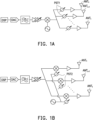
- FIG. 1A to FIG. 1D are schematic views of systems of architectures of various conventional beamformers used for array antenna.
- a digital signal processor (DSP) and a digital to analog converter (DAC) are used to generate analog signals to be transmitted by antennas ANT 1 to ANT n .
- the architecture of the beamformer used for array antenna includes several phase shifters (such as PST1, PST2, PST3, or PST4).
- the disadvantage of using a phase shifter is that the signal loss of the phase shifter increases as frequency increases. For the operating frequency bands beyond millimeter wave, the signal loss of phase shifter may reach 5 to 6 dB.
- the phase of the fed signal before into the phase shifter is greatly affected by the difference in lengths of feeding paths and the phase variations become more severe as in a higher operating frequency.
- multiple sets of mixers are added.
- the additions of amplifiers are necessary to provide the required power for the local-oscillating ends of the mixers.
- the length of a transmission line and the addition of an inductor will occupy a lot of chip area and take more cost.
- the disclosure provides an analog beamformer used for array antenna without a phase shifter and an operating method thereof, which can avoid power loss issues of signals flowing through the phase shifter, and can effectively avoid the problems of the amplitude error and the phase error suffering from the usage of phase shifter so as to minimize the estimation error of reference symbol received power (RSRP),.
- RSRP reference symbol received power
- the disclosure is also conducive to realize the feeding path layout of millimeter-wave beamforming circuit.
- An analog beamformer used for array antenna of the disclosure includes an intermediate-frequency amplifying circuit, multiple local oscillators, multiple mixers, multiple radio-frequency amplifying circuits, and a frequency locking circuit.
- the intermediate-frequency amplifying circuit receives a baseband signal to provide an intermediate-frequency signal. Power supplies or grounding ports of several local oscillators are connected together to generate frequency synchronization. At the same time, a phase difference is formed, and multiple local-oscillating signals with consistent frequency but different phases are provided.
- the local oscillators are under the control of different oscillating-frequency-control signal, respectively.
- the mixers individually receive the intermediate-frequency signal and one of the local oscillating signals, and the mixers provide multiple mixed signals.
- radio-frequency amplifying circuits receive the mixed signals to provide multiple radio-frequency signals with consistent frequency but different phases to different antennas.
- the radio-frequency signals received by each antenna have consistent frequency but different phases, so as to form directional radio-frequency signal transmission or reception.
- the frequency locking circuit is only coupled to one of the local oscillators and then lock in the frequency of the coupled local oscillator.
- An operating method of an analog beamformer used for array antenna of the disclosure includes at least the following steps.
- a baseband signal is amplified by an intermediate-frequency amplifying circuit to generate an intermediate-frequency signal.
- Multiple local-oscillating signals are provided by multiple local oscillators. Free-running frequencies of multiple local oscillators are under the controls of different oscillating-frequency-control signals. Power supplies or grounding ports of multiple local oscillators are connected together. After the DC power supply nodes or the grounding ports are connected, the frequencies of the local-oscillating signals from the local oscillators are kept the same as and consistent with that of one local oscillator which is coupled with and connected with the frequency locking circuit, but different from the original free-running frequencies.
- All of the local oscillators tend to be consistent with the same frequency and deviate from the original free running frequencies, but there is a phase difference between the local-oscillating signals of the local oscillators.
- As one of the local oscillators followed by the other local oscillators its oscillating-frequency thereof is locked by a frequency locking circuit.
- the intermediate-frequency signal and one of the local-oscillating signals are individually mixed by multiple mixers to generate one of multiple mixed signals.
- the mixed signals are amplified by multiple radio-frequency amplifying circuits to provide multiple radio-frequency signals with different phases to multiple antennas.
- connection for connection of the power supplies or the grounding ports between different local oscillators, the connection may be only implemented at the power supplies, the connection may be only implemented at the grounding ports, or the connection may be implemented at both of the power supplies and the grounding ports.
- the analog beamformer used for array antenna and the operating method thereof can achieve the same phase adjustment function as the phase shifter by the disclosed resonant network of frequency-and-phase-locking formed by connecting the power supplies or the grounding ports of the local oscillators. Since there is no shortcoming as caused as using the phase shifter, the signal transmission power loss of the phase shifter can be avoided, and the amplitude error and the phase error of the phase shifter can be effectively avoided, so as to avoid the estimation error of the reference symbol received power. Also, the design methodology of local oscillator is different from the phase shifter, the usage of transmission line and inductor is minimized, so the occupied circuit area is smaller. It is conducive to realize the feeding path layout of millimeter-wave beamforming integrated circuit.
- the disclosure is designed for a beamformer used in an array antenna system of a base station, a mobile terminal, and a radar.
- phase shifter loss there are issues of phase shifter loss, amplitude error, and phase error when implementing the beamforming function by analog technology.
- the length of a feeder path before and after the phase shifter affects the phase of the final antenna radiation signal.
- the routing arrangement of the feeder path before and after the phase shifter becomes more and more difficult, especially for the massive antenna array.
- the disclosure proposes a new analog beamforming architecture to be used for array antenna without using phase shifter.
- An analog beamformer of the disclosure used for array antenna not only reduces power loss, but also avoids the estimation error of reference symbol received power.
- This kind of analog beamformer topology will greatly present its superiority as the operating frequency becoming higher, e.g. millimeter wave.
- the advantages of this method can be more apparent and conspicuous, especially in terms of layout routing.
- FIG. 2 is a schematic view of a system of an analog beamformer used for array antenna according to an embodiment of the disclosure.
- an analog beamformer used for array antenna 100 includes a processor 110, a digital to analog converter 120, a frequency locking circuit 130, an intermediate-frequency amplifying circuit VGA IF , multiple local oscillators OSC 1 to OSC n , multiple first power-supply-elements ELi to ELn, a second power-supply-element Eva, multiple first grounding-port-elements ER 1 to ERn, a second grounding-port-element EGa, multiple radio-frequency amplifying circuits VGA 1 to VGAn, multiple mixers Mixer 1 to Mixer n , and multiple antennas ANT 1 to ANT n , where n is a positive integer and is greater than or equal to 2.
- the processor 110 is, for example, a digital signal processor, and the intermediate-frequency amplifying circuit VGA IF and the radio-
- the processor 110 receives data D TX to be transmitted to generate a signal S TX , to be transmitted wherein the processor 110 is, for example, a digital signal processor.
- the digital to analog converter 120 connecting the processor 110 receives the signal S TX which is generated from the processor 110, and subsequently converts the signal S TX to be a baseband signal S BB .
- the intermediate-frequency amplifying circuit VGA IF after the digital to analog converter 120 amplifies the baseband signal S BB and provides an intermediate-frequency signal S IF .
- the DC-bias nodes of local oscillators OSC 1 to OSC n can be connected by the first connecting elements EL 1 to EL n , respectively, and afterwards connect together to the DC power supply Vdd via the second power-supply-element Eva to form a resonant network of frequency-and-phase-locking.
- the grounding ports of local oscillators OSC 1 to OSC n can also connect the first grounding-port-elements ER 1 to ER n , respectively, and afterwards connect together to an external ground terminal via the second grounding-port-element EGa to form a resonant network of frequency-and-phase-locking.
- the local oscillators OSC 1 to OSC n provide multiple local-oscillating signals CLKL 1 to CLKL n , wherein the local oscillators OSC 1 to OSC n are under the control of different oscillating-frequency-control signals V Ctrl_1 to V Ctrl_n to setup the free-running frequencies thereof.
- the frequency locking circuit 130 is coupled to one of the local oscillators, for instance OSC 1 , to lock the frequency of the local-oscillating signal CLKL 1 of the local oscillator OSC 1 , wherein the local oscillator OSC 1 connected to the frequency locking circuit 130 may be regarded as a master oscillator, and the local oscillators OSC 2 to OSC n may be regarded as slave oscillators whose oscillation frequencies will follow up the oscillating-frequency of the master oscillator (such as the local oscillator OSC 1 ) and then deviate from its original free-running-frequency.
- the local oscillator OSC 1 may be regarded as a master oscillator
- the local oscillators OSC 2 to OSC n may be regarded as slave oscillators whose oscillation frequencies will follow up the oscillating-frequency of the master oscillator (such as the local oscillator OSC 1 ) and then deviate from its original free-running-frequency.
- the master oscillator controls the oscillation frequencies of the slave oscillators, and the phases of the local-oscillating signals of the slave oscillators become dependent on the oscillating-frequency-control signals V Ctrl_1 to V Ctrl_n .
- the mixers Mixer 1 to Mixer n are commonly coupled to the intermediate-frequency amplifying circuit VGA IF to simultaneously receive the intermediate-frequency signal S IF and individually mix with one of the local-oscillating signals CLKL 1 to CLKL n in the same frequency but different phase. Therefore, the mixers Mixer 1 to Mixer n can individually provide mixed signals (such as S mx1 to S mxn ) with different phases based on the received intermediate-frequency signal S IF and the received local-oscillating signals (such as CLKL 1 to CLKL n ) with different phases.
- the radio-frequency amplifying circuits VGA 1 to VGA n after the mixers Mixer 1 to Mixer n will amplify one of the mixed signals Smxi to Smx n into radio-frequency signal (such as S RF1 to S RFn ) with different phase based on the received mixed signals (such as Smxi to Smx n ).
- the antennas ANT 1 to ANT n receive the radio-frequency signals S RF1 to S RFn .
- grounding ports of the local oscillators OSC 1 to OSC n are connected together to form a resonant network. It also applies to the DC-bias nodes to form a resonant network.
- the frequencies of the local-oscillating signals CLKL 1 to CLKL n are synchronized to be the same frequency due to the existence of the resonant network.
- Different oscillating-frequency-control signals V Ctrl_1 to V Ctrl_n will create different free-running frequencies for the local-oscillating signals CLKL 1 to CLKL n .
- phase differences happen between the local oscillators OSC 1 to OSC n . This phenomenon is similar to the functionality of the phase shifter after the frequencies are coherent.
- phase shifting of the signals is achieved through the coherent local oscillators OSC 1 to OSC n , there is no drawback due to the use of the phase shifter, in which takes significant power loss and embeds with some amplitude/phase error. Therefore, this way can minimize the estimation error of the reference symbol received power.
- the circuits topology of the local oscillators OSC 1 to OSC n unlike the phase shifter, as implemented in semiconductor integrated-circuit technology, it will occupy fewer area and becomes more attractive for the case of millimeter-wave beamformer.
- the DC-bias nodes of local oscillators OSC 1 to OSC n are coupled to a power supply voltage Vdd by a network of the first power-supply-elements ELi to EL n and the second power-supply-element Eva.
- the grounding ports of local oscillators OSC 1 to OSC n are coupled to an external ground terminal by the first grounding-port-elements ER 1 to ER n and the second grounding-port-element EGa.
- the second power-supply-element EVa has one end tied to the power supply voltage Vdd, and the first power-supply-elements ELi to EL n are individually connected between the corresponding DC-bias nodes of the local oscillators OSC 1 to OSC n and another end of the second power-supply-element EVa.
- the second grounding-port-element EGa has one end coupled to the external grounding terminal, and the first grounding-port-elements ER 1 to ERn are individually connected between the corresponding grounding ports of the local oscillators OSC 1 to OSC n and another end of the second grounding-port-element EGa.
- the second power-supply-element EVa, the first power-supply-elements EL 1 to EL n , the second grounding-port-element EGa, and the first grounding-port-elements ER 1 to ER n individually include one of a resistor, an inductor, a capacitor, a microstrip, a coaxial cable, and a waveguide, which are determined by the frequencies of the radio-frequency signals S RF1 to S RFn .
- the frequency locking circuit 130 is only coupled to the local oscillator OSC 1 , but in other embodiments, the frequency locking circuit 130 may be only coupled to one of the local oscillators OSC 2 to OSC n , which may be determined according to the feasibility of circuit layout, and the embodiment of the disclosure is not limited thereto.
- the analog beamformer used for array antenna 100 further includes a low-frequency quartz oscillator 140 and a memory 150 coupled to the processor 110.
- the low-frequency quartz oscillator 140 provides a reference clock signal required for the operation of the processor 110, and the memory 150 stores data to be processed (such as the data to be transmitted D TX ) by the processor 110.
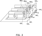
- FIG. 3 illustrates the assembly of beamformer boards and antennas with embedding a connection between the grounding ports of multiple local oscillators in the beamformer according to the embodiment of the disclosure.
- each beamformer circuit board may be regarded as a single radio-frequency channel, which is at least configured with the corresponding local oscillator (such as OSC 1 to OSCn), the corresponding mixer (such as Mixer 1 to Mixern), and the corresponding radio-frequency amplifying circuit (such as VGA 1 to VGA n ).
- Each beamformer circuit board contacts the corresponding antenna (such as ANT 1 to ANT n ).
- the spacing between the beamformer circuit boards may be 0.5 ⁇ RF , that is, 1/2 of the wavelength of the radio-frequency signal (such as S RF1 to S RFn ), and the spacing between center points of electrodes of the antennas (such as ANT 1 to ANT n ) may also be 0.5 ⁇ RF .
- FIG. 4A is a time-domain view and shows the phase difference between the waveforms generated by analog beamformers used for array antenna according to an embodiment of the disclosure. Please refer to FIG. 1 and FIG. 4A .
- the frequencies of the local-oscillating signals CLKL 1 to CLKL n are determined by the frequency of the local-oscillating signal (such as CLKL 1 ) of the master oscillator, and output phases of the local-oscillating signals (such as CLKL 1 to CLKL n ) of the slave oscillators are determined by the voltage levels of the received oscillating-frequency control signals (such as V Ctrl_1 to V Ctrl_n ).
- the adjustments of the voltage levels of the oscillating-frequency-control signals (such as V Ctrl_1 to V Ctrl_n ) of the slave oscillators affect the output phases of the local-oscillating signals (such as C LKL1 to C LKLn ).
- the selection of the main oscillator is not limited to the local oscillator OSC 1 , but may also be one of the other local oscillators OSC 2 to OSC n , which is determined according to feasible considerations of circuit layout.
- One of the local oscillators (such as the local oscillators OSC 1 to OSC n ) coupled with the frequency locking circuit 130 becomes the master oscillator, and the rest are slave oscillators.
- FIG. 4B shows the phase difference variation situation of other local oscillators with voltage levels of oscillating-frequency-control signals unchanged when a voltage level of an oscillating-frequency-control signal (such as V Ctrl_2 ) of one of multiple slave oscillators of the analog beamformer used for array antenna is adjusted according to an embodiment of the disclosure. Please refer to FIG. 1 , FIG. 4A, and FIG. 4B .
- V Ctrl_2 an oscillating-frequency-control signal
- the overall frequencies of the local-oscillating signals CLKL 1 to CLKL n are determined by the frequency of the local-oscillating signal (such as CLKL 1 ) of the master oscillator, and the output phases of the local-oscillating signals (such as CLKL 2 to CLKL n ) of the slave oscillators are determined by the voltage levels of the received oscillating-frequency-control signals (such as V Ctrl_2 to V Ctrl_n ). As shown by curves 460 and 470 in FIG.
- the voltage levels of the oscillating-frequency-control signals (such as V Ctrl_2 to V Ctrl_n ) of the slave oscillators can be used as adjustment (as shown by the curve 460 in FIG. 4B ) of the output phase of the output clock signal (such as CLKL 1 to CLKL n ), but have minor impact (as shown by the curve 470 in FIG. 4B ) on the output phases of the oscillating-signals (such as CLKL 1 to CLKL n ) by other slave oscillators.
- FIG. 5A to FIG. 5C depicts antenna gain-patterns of an analog beamformer used for array antenna at different output phase differences according to an embodiment of the disclosure.
- FIG. 5A shows an antenna gain- pattern of the radio-frequency signals S RF1 to S RFn with an output phase difference of -60°
- FIG. 5B shows an antenna gain-pattern of the radio-frequency signals S RF1 to S RFn with an output phase difference of -30°
- FIG. 5C shows an antenna gain-pattern of the radio-frequency signals S RF1 to S RFn with an output phase difference of 0°.
- the spatial resolutions of the field patterns are similar, but the antenna gain-pattern with the output phase difference of -60° generates a grating lobe effect.
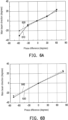
- FIG. 6A illustrates the relationship between main lobe direction and output phase for a 1x2 array antenna according to an embodiment of the disclosure.
- FIG. 6B is another case for a 1x3 array antenna.
- a curve 610 is a measured relationship between a main beam direction of a radio-frequency signal emitted by a 1x2 array antenna and an output phase difference of the radio-frequency signal
- a curve 620 is a calculated relationship between the main beam direction of the radio-frequency signal emitted by the 1x2 array antenna and the output phase difference of the radio-frequency signal.
- the measured relationship substantially matches the calculated one.
- a curve 630 is a measured relationship between a main beam direction of a radio-frequency signal emitted by a 1x3 array antenna and an output phase difference of the radio-frequency signal
- a curve 640 is a calculated relationship between the main beam direction of the radio-frequency signal emitted by the 1x3 array antenna and the output phase difference of the radio-frequency signal. As shown by the curves 630 and 640, the measured relationship substantially matches the calculated relationship.
- FIG. 7 is a schematic view of a an analog beamformer used for array antenna according to another embodiment of the disclosure, which only implements connection by elements at power supply terminal. Please refer to FIG. 2 and FIG. 7 .
- an analog beamformer used for array antenna 200 is substantially the same as the analog beamformer used for array antenna 100, and the difference is that the analog beamformer used for array antenna 200 omits the first grounding-port-elements ER 1 to ERn and the second grounding-port-element EGa, that is, the grounding ports of the local oscillators OSC 1 to OSC n are directly connected to the external grounding terminal.
- FIG. 8 is a schematic view of an analog beamformer used for array antenna according to another embodiment of the disclosure, which only implements connection by elements at grounding ports. Please refer to FIG. 2 and FIG. 8 .
- an analog beamformer used for array antenna 300 is substantially the same as the analog beamformer used for array antenna 100, and the difference is that the analog beamformer used for array antenna 300 omits the first power-supply-elements EL 1 to EL n and the second power-supply-element Eva, that is, the DC-bias nodes of the local oscillators OSC 1 to OSC n receive the power supply voltage Vdd, respectively.
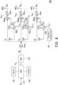
- FIG. 9A shows the pin assignments of a single integrated circuit used for a beamformer in which connection by elements is applied to both DC-bias pin P V_OSG and grounding pin P GND_OSG according to an embodiment of the disclosure.
- each local oscillator OSC x and a coupled first power-supply-element EL x , a coupled first grounding-port-element ER x , a coupled mixer Mixer x , and a corresponding radio-frequency amplifying circuit VGA x are encapsulated into a single integrated circuit chipi, where x is an index number.
- the integrated circuit chipi has pins P IF , P V_OSC , P Locking , P Ctrl , P GND_OSC , P GND_Others , P_ANT, P V_VGA , and P V_mixer .
- the pin P IF is coupled to an input end of the mixer Mixer x .
- the first power-supply-element EL x is coupled between the pin P V_OSC and the DC-bias node of the local oscillator OSC x .
- the pin P Locking is coupled to a reference frequency end of the local oscillator OSC x .
- the pin P Ctrl is coupled to a free-running-frequency control end of the local oscillator OSC x .
- the first grounding-port-element ER x is coupled between the pin P GND_OSC and a grounding port of the local oscillator OSC x .
- the pin P GND_Others is coupled to grounding ports of the mixer Mixer x and the radio-frequency amplifying circuit VGA x .
- the pin P_ANT is coupled to an output end of the radio-frequency amplifying circuit VGA x .
- the pin P V_VGA is coupled to a power supply of the radio-frequency amplifying circuit VGA x .
- the pin P V_mixer is coupled to a power supply of the mixer Mixer x .
- FIG. 9B shows the assembly of an analog beamformer used for array antenna using the single integrated circuit chipi shown in FIG. 9A according to an embodiment of the disclosure. Please refer to FIG. 2 , FIG. 9A , and FIG. 9B .
- the same or similar elements use the same or similar reference numerals.
- integrated circuits chip 11 to chip 1n are the same as the integrated circuit chip 1 .
- the pins P IF of the integrated circuits chip 11 to chip 1n are all coupled to an output end of the intermediate-frequency amplifying circuit VGA IF .
- the pins P V_OSC of the integrated circuits chip 11 to chip 1n are all coupled to one end of the second power-supply-element EVa.
- the pin P Locking of only the integrated circuit chip 11 is coupled to the frequency locking circuit 130.
- the pins P GND_OSC of the integrated circuits chip 11 to chip 1n are all coupled to one end of the second grounding-port-element EGa.
- the pins P GND_Others of the integrated circuits chip 11 to chip 1n are independently connected to a different external grounding terminal.
- the pins P_ANT of the integrated circuits chip 11 to chip 1n are respectively coupled to the antennas ANT 1 to ANT n .
- the P V_mixer and P V_VGA of the integrated circuits chip 11 to chip 1n should receive corresponding power supply voltages to drive the mixer Mixer x and the radio-frequency amplifying circuit VGA x to operate.
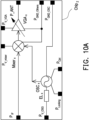
- FIG. 10A shows the pin assignments of a single integrated circuit used for a beamformer in which connection by elements is only applied to DC-bias pin P V_OSC according to an embodiment of the disclosure.
- An integrated circuit chip 2 is substantially the same as the integrated circuit chipi, and the difference is that the first grounding-port-element ER x is omitted in chip 2 . That is, each local oscillator OSC x and the coupled first power-supply-element EL x , the coupled mixer Mixer x , and the corresponding radio-frequency amplifying circuit VGA x are encapsulated into the single integrated circuit chip 2 .
- the pin P GND_OSC directly plays a role of grounding port of the local oscillator OSC x . It will be directly connected to an external independent grounding terminal.
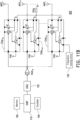
- FIG. 10B shows the assembly an analog beamformer used for array antenna system using the single integrated circuit chip 2 shown in FIG. 10A according to an embodiment of the disclosure. Please refer to FIG. 9B , FIG. 10A , and FIG. 10B .
- the same or similar elements use the same or similar reference numerals.
- integrated circuits chip 21 to chip 2n are the same as the integrated circuit chip 2
- the difference between the analog beamformer used for array antenna 500 and the analog beamformer used for array antenna 400 is that the pins P GND_OSC of the integrated circuits chip 21 to chip 2n are directly connected to multiple external grounding terminals.
- FIG. 11A shows the pin assignments of a single integrated circuit used for a beamformer in which connection by elements is only applied to grounding pin P GND_OSG according to an embodiment of the disclosure.
- An integrated circuit chip 3 is substantially the same as the integrated circuit chipi, and the difference is that the first power-supply-element EL x is omitted. That is, each local oscillator OSC x and the coupled first grounding-port-element ER x , the coupled mixer Mixer x , and the corresponding radio-frequency amplifying circuit VGA x are encapsulated into the single integrated circuit chip 3 .
- the pin P V_OSC directly plays a role of the DC-bias nodes of the local oscillators. It will be directly connected to the external power supply.
- FIG. 11B shows the assembly of an analog beamformer used for array antenna using the single integrated circuit chip 3 shown in FIG. 11A according to an embodiment of the disclosure. Please refer to FIG. 9B , FIG. 11A , and FIG. 11B .
- the same or similar elements use the same or similar reference numerals.
- integrated circuits chip 31 to chip 3n are the same as the integrated circuit chip 3 , and the difference between the analog beamformer used for array antenna 600 and the analog beamformer used for array antenna 400 is that the pins P V_OSC of the integrated circuits chip 31 to chip 3n directly connected to external power supply Vdd.
- FIG. 12 is a flowchart of the operating method of an analog beamformer used for array antenna according to an embodiment of the disclosure. Please refer to FIG. 12 .
- the operating method of the analog beamformer used for array antenna includes at least the following steps.
- Step S110 a baseband signal is amplified by an intermediate-frequency amplifying circuit to generate an intermediate-frequency signal.
- Step S120 multiple local-oscillating signals are provided by multiple local oscillators, wherein power supplies or grounding ports of the local oscillators are connected together to form a resonant network of frequency-and-phase-locking.
- the local oscillators are under the control of different oscillating-frequency-control signal, respectively.
- Step S130 Only one of the local oscillators is locked by a frequency locking circuit such as phase lock loop.
- Step S130 the intermediate-frequency signal and one of the local-oscillating signals are individually mixed by multiple mixers to generate one of multiple mixed signals with different phase.
- Step S140 the mixed signals with different phase are amplified by multiple radio-frequency amplifying circuits to provide multiple radio-frequency signals with different phases to multiple antennas.
- the sequence of Steps S110, S120, S130, and S140 is for illustration, and the embodiment of the disclosure is not limited thereto. Also, for the details of Steps S110, S120, S130, and S140, reference may be made to the embodiments shown in FIG. 2 , FIG. 3 , FIG. 4A, FIG. 4B , FIG.
- the analog beamformer used for array antenna and the operating method thereof can achieve the same functionality like a phase shifter by connecting the local oscillators to form the resonant network of frequency-and-phase-locking. Since there is no disadvantage due to the use of the phase shifter, power loss can be reduced. In the meantime, the amplitude error and the phase error of the phase shifter can be effectively avoided, and then the estimation error of the reference symbol received power is minimized. Also, the local oscillators unlike the phase shifter, the occupied integrated-circuit area is smaller. It is good for the implementation and realization of the millimeter-wave beamforming circuit.
Landscapes
- Engineering & Computer Science (AREA)
- Computer Networks & Wireless Communication (AREA)
- Signal Processing (AREA)
- Power Engineering (AREA)
- Variable-Direction Aerials And Aerial Arrays (AREA)
Abstract
Description
- The disclosure relates to a beamformer, and particularly relates to an analog beamformer used for array antenna and an operating method thereof.
- The beamformer is an important circuit for providing directional emission of electromagnetic energy. Radars for military purposes have been widely used and have also recently expanded the use in mobile communications. The directional emission is necessary especially above the millimeter waveband, and the beamformer has become a key technology for short-wavelength mobile communications.
-
FIG. 1A to FIG. 1D are schematic views of systems of architectures of various conventional beamformers used for array antenna. A digital signal processor (DSP) and a digital to analog converter (DAC) are used to generate analog signals to be transmitted by antennas ANT1 to ANTn. As shown inFIG. 1A to FIG. 1D , the architecture of the beamformer used for array antenna includes several phase shifters (such as PST1, PST2, PST3, or PST4). The disadvantage of using a phase shifter is that the signal loss of the phase shifter increases as frequency increases. For the operating frequency bands beyond millimeter wave, the signal loss of phase shifter may reach 5 to 6 dB. In the architecture of the beamformer used for array antenna shown inFIG. 1A , the phase of the fed signal before into the phase shifter is greatly affected by the difference in lengths of feeding paths and the phase variations become more severe as in a higher operating frequency. In the architecture of the beamformer used for array antenna shown inFIG. 1B to FIG. 1D , multiple sets of mixers are added. In the architecture of the beamformer used for array antenna shown inFIG. 1B , before allocating local-oscillating signals to different mixers, the additions of amplifiers are necessary to provide the required power for the local-oscillating ends of the mixers. Also, in the architecture of the beamformer used for array antenna using the phase shifter, as it is implemented as an integrated circuit by a semiconductor process, the length of a transmission line and the addition of an inductor will occupy a lot of chip area and take more cost. - The disclosure provides an analog beamformer used for array antenna without a phase shifter and an operating method thereof, which can avoid power loss issues of signals flowing through the phase shifter, and can effectively avoid the problems of the amplitude error and the phase error suffering from the usage of phase shifter so as to minimize the estimation error of reference symbol received power (RSRP),. The disclosure is also conducive to realize the feeding path layout of millimeter-wave beamforming circuit.
- An analog beamformer used for array antenna of the disclosure includes an intermediate-frequency amplifying circuit, multiple local oscillators, multiple mixers, multiple radio-frequency amplifying circuits, and a frequency locking circuit. The intermediate-frequency amplifying circuit receives a baseband signal to provide an intermediate-frequency signal. Power supplies or grounding ports of several local oscillators are connected together to generate frequency synchronization. At the same time, a phase difference is formed, and multiple local-oscillating signals with consistent frequency but different phases are provided. The local oscillators are under the control of different oscillating-frequency-control signal, respectively. The mixers individually receive the intermediate-frequency signal and one of the local oscillating signals, and the mixers provide multiple mixed signals. Several radio-frequency amplifying circuits receive the mixed signals to provide multiple radio-frequency signals with consistent frequency but different phases to different antennas. The radio-frequency signals received by each antenna have consistent frequency but different phases, so as to form directional radio-frequency signal transmission or reception. The frequency locking circuit is only coupled to one of the local oscillators and then lock in the frequency of the coupled local oscillator.
- An operating method of an analog beamformer used for array antenna of the disclosure includes at least the following steps. A baseband signal is amplified by an intermediate-frequency amplifying circuit to generate an intermediate-frequency signal. Multiple local-oscillating signals are provided by multiple local oscillators. Free-running frequencies of multiple local oscillators are under the controls of different oscillating-frequency-control signals. Power supplies or grounding ports of multiple local oscillators are connected together. After the DC power supply nodes or the grounding ports are connected, the frequencies of the local-oscillating signals from the local oscillators are kept the same as and consistent with that of one local oscillator which is coupled with and connected with the frequency locking circuit, but different from the original free-running frequencies. All of the local oscillators tend to be consistent with the same frequency and deviate from the original free running frequencies, but there is a phase difference between the local-oscillating signals of the local oscillators. As one of the local oscillators followed by the other local oscillators, its oscillating-frequency thereof is locked by a frequency locking circuit. Then, the intermediate-frequency signal and one of the local-oscillating signals are individually mixed by multiple mixers to generate one of multiple mixed signals. The mixed signals are amplified by multiple radio-frequency amplifying circuits to provide multiple radio-frequency signals with different phases to multiple antennas.
- In the embodiments of the disclosure, for connection of the power supplies or the grounding ports between different local oscillators, the connection may be only implemented at the power supplies, the connection may be only implemented at the grounding ports, or the connection may be implemented at both of the power supplies and the grounding ports.
- Based on the above, the analog beamformer used for array antenna and the operating method thereof according to the embodiments of the disclosure can achieve the same phase adjustment function as the phase shifter by the disclosed resonant network of frequency-and-phase-locking formed by connecting the power supplies or the grounding ports of the local oscillators. Since there is no shortcoming as caused as using the phase shifter, the signal transmission power loss of the phase shifter can be avoided, and the amplitude error and the phase error of the phase shifter can be effectively avoided, so as to avoid the estimation error of the reference symbol received power. Also, the design methodology of local oscillator is different from the phase shifter, the usage of transmission line and inductor is minimized, so the occupied circuit area is smaller. It is conducive to realize the feeding path layout of millimeter-wave beamforming integrated circuit.
- In order for the features and advantages of the disclosure to be more comprehensible, the following specific embodiments are described in detail in conjunction with the accompanying drawings.
-
-
FIG. 1A to FIG. 1D are the architecture views of various conventional beamformers used for array antenna. -
FIG. 2 is a schematic view of an analog beamformer used for array antenna in which connecting by elements is implemented at both power supply sides and grounding terminals according to an embodiment of the disclosure. -
FIG. 3 illustrates the assembly of beamformer boards and antennas with embedding a connection between the ground ports of multiple local oscillators in the beamformer according to the embodiment of the disclosure. -
FIG. 4A is a time-domain view showing the phase difference between waveforms generated by analog beamformers used for array antenna according to an embodiment of the disclosure. -
FIG. 4B shows the phase variation situation when an oscillating-frequency-control signal being applied to a local oscillator of the analog beamformer used for array antenna according to the embodiment of the disclosure. In the meantime, the oscillating-frequency-control signals of other local oscillators are kept unchanged and their phase characteristics are almost no change. -
FIG. 5A to FIG. 5C depict the antenna gain-patterns of an analog beamformer used for array antenna at different output phase differences according to an embodiment of the disclosure. -
FIG. 6A illustrates the relationship between main lobe direction and output phase for a 1x2 array antenna according to an embodiment of the disclosure.FIG. 6B is another case for a 1x3 array antenna. -
FIG. 7 is a schematic view of an analog beamformer used for array antenna in which connection by elements is only implemented at power supply terminals according to another embodiment of the disclosure. -
FIG. 8 is a schematic view of an analog beamformer used for array antenna in which connection by elements is only implemented at grounding terminals according to another embodiment of the disclosure. -
FIG. 9A is a function-block view of a single integrated circuit used in a beamformer, in which connecting nodes by elements are reserved to both power supplies and grounding ports according to an embodiment of the disclosure. -
FIG. 9B is the implementation of an analog beamformer used for array antenna using multiple integrated circuits shown inFIG. 9A . Both of the power supplies and the grounding terminals are separately off-chip connected by elements according to an embodiment of the disclosure. -
FIG. 10A is a function-block view of a single integrated circuit used in a beamformer in which connecting nodes by elements are reserved and only applied to power supply nodes according to an embodiment of the disclosure. -
FIG. 10B is the implementation of an analog beamformer used for array antenna using multiple integrated circuits shown inFIG. 10A . In this case, only power supply terminals are off-chip connected by elements according to an embodiment of the disclosure. -
FIG. 11A is a function-block view of a single integrated circuit used in a beamformer in which connecting nodes by elements are reserved and only applied to grounding terminals according to an embodiment of the disclosure. -
FIG. 11B is the implementation of an analog beamformer used for array antenna using the multiple integrated circuits shown inFIG. 11A . In this case, in which connecting by elements is only applied to the grounding terminals according to an embodiment of the disclosure. -
FIG. 12 is a flowchart of the operating method of an analog beamformer used for array antenna according to an embodiment of the disclosure. - The disclosure is designed for a beamformer used in an array antenna system of a base station, a mobile terminal, and a radar. At present, there are issues of phase shifter loss, amplitude error, and phase error when implementing the beamforming function by analog technology. Moreover, the length of a feeder path before and after the phase shifter affects the phase of the final antenna radiation signal. In a higher frequency band such as millimeter wave and above, the routing arrangement of the feeder path before and after the phase shifter becomes more and more difficult, especially for the massive antenna array.
- Compared with the prior art that are mostly implemented by injection locking or coupling network, the disclosure proposes a new analog beamforming architecture to be used for array antenna without using phase shifter.
- An analog beamformer of the disclosure used for array antenna not only reduces power loss, but also avoids the estimation error of reference symbol received power. This kind of analog beamformer topology will greatly present its superiority as the operating frequency becoming higher, e.g. millimeter wave. Moreover, for the array antenna system with a large number of antennas, the advantages of this method can be more apparent and conspicuous, especially in terms of layout routing.
-
FIG. 2 is a schematic view of a system of an analog beamformer used for array antenna according to an embodiment of the disclosure. Please refer toFIG. 2 . In the embodiment, an analog beamformer used forarray antenna 100 includes aprocessor 110, a digital toanalog converter 120, afrequency locking circuit 130, an intermediate-frequency amplifying circuit VGAIF, multiple local oscillators OSC1 to OSCn, multiple first power-supply-elements ELi to ELn, a second power-supply-element Eva, multiple first grounding-port-elements ER1 to ERn, a second grounding-port-element EGa, multiple radio-frequency amplifying circuits VGA1 to VGAn, multiple mixers Mixer1 to Mixern, and multiple antennas ANT1 to ANTn, where n is a positive integer and is greater than or equal to 2. Theprocessor 110 is, for example, a digital signal processor, and the intermediate-frequency amplifying circuit VGAIF and the radio-frequency amplifying circuits VGA1 to VGAn are, for example, variable gain amplifiers. - The
processor 110 receives data DTX to be transmitted to generate a signal STX, to be transmitted wherein theprocessor 110 is, for example, a digital signal processor. The digital toanalog converter 120 connecting theprocessor 110 receives the signal STX which is generated from theprocessor 110, and subsequently converts the signal STX to be a baseband signal SBB. The intermediate-frequency amplifying circuit VGAIF after the digital toanalog converter 120 amplifies the baseband signal SBB and provides an intermediate-frequency signal SIF. - The DC-bias nodes of local oscillators OSC1 to OSCn can be connected by the first connecting elements EL1 to ELn, respectively, and afterwards connect together to the DC power supply Vdd via the second power-supply-element Eva to form a resonant network of frequency-and-phase-locking. The grounding ports of local oscillators OSC1 to OSCn can also connect the first grounding-port-elements ER1 to ERn, respectively, and afterwards connect together to an external ground terminal via the second grounding-port-element EGa to form a resonant network of frequency-and-phase-locking. The local oscillators OSC1 to OSCn provide multiple local-oscillating signals CLKL1 to CLKLn, wherein the local oscillators OSC1 to OSCn are under the control of different oscillating-frequency-control signals VCtrl_1 to VCtrl_n to setup the free-running frequencies thereof. The
frequency locking circuit 130 is coupled to one of the local oscillators, for instance OSC1, to lock the frequency of the local-oscillating signal CLKL1 of the local oscillator OSC1, wherein the local oscillator OSC1 connected to thefrequency locking circuit 130 may be regarded as a master oscillator, and the local oscillators OSC2 to OSCn may be regarded as slave oscillators whose oscillation frequencies will follow up the oscillating-frequency of the master oscillator (such as the local oscillator OSC1) and then deviate from its original free-running-frequency. The master oscillator controls the oscillation frequencies of the slave oscillators, and the phases of the local-oscillating signals of the slave oscillators become dependent on the oscillating-frequency-control signals VCtrl_1 to VCtrl_n. - The mixers Mixer1 to Mixern are commonly coupled to the intermediate-frequency amplifying circuit VGAIF to simultaneously receive the intermediate-frequency signal SIF and individually mix with one of the local-oscillating signals CLKL1 to CLKLn in the same frequency but different phase. Therefore, the mixers Mixer1 to Mixern can individually provide mixed signals (such as Smx1 to Smxn) with different phases based on the received intermediate-frequency signal SIF and the received local-oscillating signals (such as CLKL1 to CLKLn) with different phases.
- The radio-frequency amplifying circuits VGA1 to VGAn after the mixers Mixer1 to Mixern will amplify one of the mixed signals Smxi to Smxn into radio-frequency signal (such as SRF1 to SRFn) with different phase based on the received mixed signals (such as Smxi to Smxn). The antennas ANT1 to ANTn receive the radio-frequency signals SRF1 to SRFn. According to the above, grounding ports of the local oscillators OSC1 to OSCn are connected together to form a resonant network. It also applies to the DC-bias nodes to form a resonant network. Therefore, the frequencies of the local-oscillating signals CLKL1 to CLKLn are synchronized to be the same frequency due to the existence of the resonant network. Different oscillating-frequency-control signals VCtrl_1 to VCtrl_n will create different free-running frequencies for the local-oscillating signals CLKL1 to CLKLn. Once the frequencies of slave oscillators are forced to be the same as the frequency of master oscillator, phase differences happen between the local oscillators OSC1 to OSCn. This phenomenon is similar to the functionality of the phase shifter after the frequencies are coherent. Since the phase shifting of the signals is achieved through the coherent local oscillators OSC1 to OSCn, there is no drawback due to the use of the phase shifter, in which takes significant power loss and embeds with some amplitude/phase error. Therefore, this way can minimize the estimation error of the reference symbol received power. Moreover, the circuits topology of the local oscillators OSC1 to OSCn, unlike the phase shifter, as implemented in semiconductor integrated-circuit technology, it will occupy fewer area and becomes more attractive for the case of millimeter-wave beamformer.
- In the embodiment of the disclosure, the DC-bias nodes of local oscillators OSC1 to OSCn are coupled to a power supply voltage Vdd by a network of the first power-supply-elements ELi to ELn and the second power-supply-element Eva. Or, the grounding ports of local oscillators OSC1 to OSCn are coupled to an external ground terminal by the first grounding-port-elements ER1 to ERn and the second grounding-port-element EGa. Furthermore, the second power-supply-element EVa has one end tied to the power supply voltage Vdd, and the first power-supply-elements ELi to ELn are individually connected between the corresponding DC-bias nodes of the local oscillators OSC1 to OSCn and another end of the second power-supply-element EVa. The second grounding-port-element EGa has one end coupled to the external grounding terminal, and the first grounding-port-elements ER1 to ERn are individually connected between the corresponding grounding ports of the local oscillators OSC1 to OSCn and another end of the second grounding-port-element EGa.
- In the embodiment of the disclosure, the second power-supply-element EVa, the first power-supply-elements EL1 to ELn, the second grounding-port-element EGa, and the first grounding-port-elements ER1 to ERn individually include one of a resistor, an inductor, a capacitor, a microstrip, a coaxial cable, and a waveguide, which are determined by the frequencies of the radio-frequency signals SRF1 to SRFn.
- In the embodiment of the disclosure, the
frequency locking circuit 130 is only coupled to the local oscillator OSC1, but in other embodiments, thefrequency locking circuit 130 may be only coupled to one of the local oscillators OSC2 to OSCn, which may be determined according to the feasibility of circuit layout, and the embodiment of the disclosure is not limited thereto. - In the embodiment of the disclosure, the analog beamformer used for
array antenna 100 further includes a low-frequency quartz oscillator 140 and amemory 150 coupled to theprocessor 110. The low-frequency quartz oscillator 140 provides a reference clock signal required for the operation of theprocessor 110, and thememory 150 stores data to be processed (such as the data to be transmitted DTX) by theprocessor 110. -
FIG. 3 illustrates the assembly of beamformer boards and antennas with embedding a connection between the grounding ports of multiple local oscillators in the beamformer according to the embodiment of the disclosure. Please refer toFIG. 2 andFIG. 3 . In the embodiment, each beamformer circuit board may be regarded as a single radio-frequency channel, which is at least configured with the corresponding local oscillator (such as OSC1 to OSCn), the corresponding mixer (such as Mixer1 to Mixern), and the corresponding radio-frequency amplifying circuit (such as VGA1 to VGAn). Each beamformer circuit board contacts the corresponding antenna (such as ANT1 to ANTn). - In the embodiment, the spacing between the beamformer circuit boards may be 0.5λRF, that is, 1/2 of the wavelength of the radio-frequency signal (such as SRF1 to SRFn), and the spacing between center points of electrodes of the antennas (such as ANT1 to ANTn) may also be 0.5λRF.
-
FIG. 4A is a time-domain view and shows the phase difference between the waveforms generated by analog beamformers used for array antenna according to an embodiment of the disclosure. Please refer toFIG. 1 andFIG. 4A . In the embodiment, the frequencies of the local-oscillating signals CLKL1 to CLKLn are determined by the frequency of the local-oscillating signal (such as CLKL1) of the master oscillator, and output phases of the local-oscillating signals (such as CLKL1 to CLKLn) of the slave oscillators are determined by the voltage levels of the received oscillating-frequency control signals (such as VCtrl_1 to VCtrl_n). As shown bycurves FIG. 4A , the adjustments of the voltage levels of the oscillating-frequency-control signals (such as VCtrl_1 to VCtrl_n) of the slave oscillators affect the output phases of the local-oscillating signals (such as CLKL1 to CLKLn). The selection of the main oscillator is not limited to the local oscillator OSC1, but may also be one of the other local oscillators OSC2 to OSCn, which is determined according to feasible considerations of circuit layout. One of the local oscillators (such as the local oscillators OSC1 to OSCn) coupled with thefrequency locking circuit 130 becomes the master oscillator, and the rest are slave oscillators. -
FIG. 4B shows the phase difference variation situation of other local oscillators with voltage levels of oscillating-frequency-control signals unchanged when a voltage level of an oscillating-frequency-control signal (such as VCtrl_2) of one of multiple slave oscillators of the analog beamformer used for array antenna is adjusted according to an embodiment of the disclosure. Please refer toFIG. 1 ,FIG. 4A, and FIG. 4B . In the embodiment, the overall frequencies of the local-oscillating signals CLKL1 to CLKLn are determined by the frequency of the local-oscillating signal (such as CLKL1) of the master oscillator, and the output phases of the local-oscillating signals (such as CLKL2 to CLKLn) of the slave oscillators are determined by the voltage levels of the received oscillating-frequency-control signals (such as VCtrl_2 to VCtrl_n). As shown bycurves FIG. 4B , the voltage levels of the oscillating-frequency-control signals (such as VCtrl_2 to VCtrl_n) of the slave oscillators can be used as adjustment (as shown by thecurve 460 inFIG. 4B ) of the output phase of the output clock signal (such as CLKL1 to CLKLn), but have minor impact (as shown by thecurve 470 inFIG. 4B ) on the output phases of the oscillating-signals (such as CLKL1 to CLKLn) by other slave oscillators. -
FIG. 5A to FIG. 5C depicts antenna gain-patterns of an analog beamformer used for array antenna at different output phase differences according to an embodiment of the disclosure. Please refer toFIG. 1 andFIG. 5A toFIG. 5C , whereinFIG. 5A shows an antenna gain- pattern of the radio-frequency signals SRF1 to SRFn with an output phase difference of -60°,FIG. 5B shows an antenna gain-pattern of the radio-frequency signals SRF1 to SRFn with an output phase difference of -30°, andFIG. 5C shows an antenna gain-pattern of the radio-frequency signals SRF1 to SRFn with an output phase difference of 0°. As shown inFIG. 5A to FIG. 5C , the spatial resolutions of the field patterns are similar, but the antenna gain-pattern with the output phase difference of -60° generates a grating lobe effect. -
FIG. 6A illustrates the relationship between main lobe direction and output phase for a 1x2 array antenna according to an embodiment of the disclosure.FIG. 6B is another case for a 1x3 array antenna. Please refer toFIG. 1 andFIG. 6A , acurve 610 is a measured relationship between a main beam direction of a radio-frequency signal emitted by a 1x2 array antenna and an output phase difference of the radio-frequency signal, and acurve 620 is a calculated relationship between the main beam direction of the radio-frequency signal emitted by the 1x2 array antenna and the output phase difference of the radio-frequency signal. As shown by thecurves - On the other hand, please refer to
FIG. 1 andFIG. 6B . Acurve 630 is a measured relationship between a main beam direction of a radio-frequency signal emitted by a 1x3 array antenna and an output phase difference of the radio-frequency signal, and acurve 640 is a calculated relationship between the main beam direction of the radio-frequency signal emitted by the 1x3 array antenna and the output phase difference of the radio-frequency signal. As shown by thecurves -
FIG. 7 is a schematic view of a an analog beamformer used for array antenna according to another embodiment of the disclosure, which only implements connection by elements at power supply terminal. Please refer toFIG. 2 andFIG. 7 . In the embodiment, an analog beamformer used forarray antenna 200 is substantially the same as the analog beamformer used forarray antenna 100, and the difference is that the analog beamformer used forarray antenna 200 omits the first grounding-port-elements ER1 to ERn and the second grounding-port-element EGa, that is, the grounding ports of the local oscillators OSC1 to OSCn are directly connected to the external grounding terminal. -
FIG. 8 is a schematic view of an analog beamformer used for array antenna according to another embodiment of the disclosure, which only implements connection by elements at grounding ports. Please refer toFIG. 2 andFIG. 8 . In the embodiment, an analog beamformer used forarray antenna 300 is substantially the same as the analog beamformer used forarray antenna 100, and the difference is that the analog beamformer used forarray antenna 300 omits the first power-supply-elements EL1 to ELn and the second power-supply-element Eva, that is, the DC-bias nodes of the local oscillators OSC1 to OSCn receive the power supply voltage Vdd, respectively. -
FIG. 9A shows the pin assignments of a single integrated circuit used for a beamformer in which connection by elements is applied to both DC-bias pin PV_OSG and grounding pin PGND_OSG according to an embodiment of the disclosure. Please refer toFIG. 2 andFIG. 9A , wherein the same or similar elements use the same or similar reference numerals. In the embodiment, each local oscillator OSCx and a coupled first power-supply-element ELx, a coupled first grounding-port-element ERx, a coupled mixer Mixerx, and a corresponding radio-frequency amplifying circuit VGAx are encapsulated into a single integrated circuit chipi, where x is an index number. The integrated circuit chipi has pins PIF, PV_OSC, PLocking, PCtrl, PGND_OSC, PGND_Others, P_ANT, PV_VGA, and PV_mixer. - The pin PIF is coupled to an input end of the mixer Mixerx. The first power-supply-element ELx is coupled between the pin PV_OSC and the DC-bias node of the local oscillator OSCx. The pin PLocking is coupled to a reference frequency end of the local oscillator OSCx. The pin PCtrl is coupled to a free-running-frequency control end of the local oscillator OSCx. The first grounding-port-element ERx is coupled between the pin PGND_OSC and a grounding port of the local oscillator OSCx. The pin PGND_Others is coupled to grounding ports of the mixer Mixerx and the radio-frequency amplifying circuit VGAx. The pin P_ANT is coupled to an output end of the radio-frequency amplifying circuit VGAx. The pin PV_VGA is coupled to a power supply of the radio-frequency amplifying circuit VGAx. The pin PV_mixer is coupled to a power supply of the mixer Mixerx.
-
FIG. 9B shows the assembly of an analog beamformer used for array antenna using the single integrated circuit chipi shown inFIG. 9A according to an embodiment of the disclosure. Please refer toFIG. 2 ,FIG. 9A , andFIG. 9B . In the embodiment, the same or similar elements use the same or similar reference numerals. In an analog beamformer used for array antenna 400, integrated circuits chip11 to chip1n are the same as the integrated circuit chip1. The pins PIF of the integrated circuits chip11 to chip1n are all coupled to an output end of the intermediate-frequency amplifying circuit VGAIF. The pins PV_OSC of the integrated circuits chip11 to chip1n are all coupled to one end of the second power-supply-element EVa. The pin PLocking of only the integrated circuit chip11 is coupled to thefrequency locking circuit 130. The pins PGND_OSC of the integrated circuits chip11 to chip1n are all coupled to one end of the second grounding-port-element EGa. The pins PGND_Others of the integrated circuits chip11 to chip1n are independently connected to a different external grounding terminal. The pins P_ANT of the integrated circuits chip11 to chip1n are respectively coupled to the antennas ANT1 to ANTn. In addition, although not shown inFIG. 9B , the PV_mixer and PV_VGA of the integrated circuits chip11 to chip1n should receive corresponding power supply voltages to drive the mixer Mixerx and the radio-frequency amplifying circuit VGAx to operate. -
FIG. 10A shows the pin assignments of a single integrated circuit used for a beamformer in which connection by elements is only applied to DC-bias pin PV_OSC according to an embodiment of the disclosure. Please refer toFIG. 9A andFIG. 10A . An integrated circuit chip2 is substantially the same as the integrated circuit chipi, and the difference is that the first grounding-port-element ERx is omitted in chip2. That is, each local oscillator OSCx and the coupled first power-supply-element ELx, the coupled mixer Mixerx, and the corresponding radio-frequency amplifying circuit VGAx are encapsulated into the single integrated circuit chip2. The pin PGND_OSC directly plays a role of grounding port of the local oscillator OSCx. It will be directly connected to an external independent grounding terminal. -
FIG. 10B shows the assembly an analog beamformer used for array antenna system using the single integrated circuit chip2 shown inFIG. 10A according to an embodiment of the disclosure. Please refer toFIG. 9B ,FIG. 10A , andFIG. 10B . In the embodiment, the same or similar elements use the same or similar reference numerals. In an analog beamformer used forarray antenna 500, integrated circuits chip21 to chip2n are the same as the integrated circuit chip2, and the difference between the analog beamformer used forarray antenna 500 and the analog beamformer used for array antenna 400 is that the pins PGND_OSC of the integrated circuits chip21 to chip2n are directly connected to multiple external grounding terminals. -
FIG. 11A shows the pin assignments of a single integrated circuit used for a beamformer in which connection by elements is only applied to grounding pin PGND_OSG according to an embodiment of the disclosure. Please refer toFIG. 9A andFIG. 11A . An integrated circuit chip3 is substantially the same as the integrated circuit chipi, and the difference is that the first power-supply-element ELx is omitted. That is, each local oscillator OSCx and the coupled first grounding-port-element ERx, the coupled mixer Mixerx, and the corresponding radio-frequency amplifying circuit VGAx are encapsulated into the single integrated circuit chip3. The pin PV_OSC directly plays a role of the DC-bias nodes of the local oscillators. It will be directly connected to the external power supply. -
FIG. 11B shows the assembly of an analog beamformer used for array antenna using the single integrated circuit chip3 shown inFIG. 11A according to an embodiment of the disclosure. Please refer toFIG. 9B ,FIG. 11A , andFIG. 11B . In the embodiment, the same or similar elements use the same or similar reference numerals. In an analog beamformer used forarray antenna 600, integrated circuits chip31 to chip3n are the same as the integrated circuit chip3, and the difference between the analog beamformer used forarray antenna 600 and the analog beamformer used for array antenna 400 is that the pins PV_OSC of the integrated circuits chip31 to chip3n directly connected to external power supply Vdd. -
FIG. 12 is a flowchart of the operating method of an analog beamformer used for array antenna according to an embodiment of the disclosure. Please refer toFIG. 12 . In the embodiment, the operating method of the analog beamformer used for array antenna includes at least the following steps. In Step S110, a baseband signal is amplified by an intermediate-frequency amplifying circuit to generate an intermediate-frequency signal. In Step S120, multiple local-oscillating signals are provided by multiple local oscillators, wherein power supplies or grounding ports of the local oscillators are connected together to form a resonant network of frequency-and-phase-locking. The local oscillators are under the control of different oscillating-frequency-control signal, respectively. Only one of the local oscillators is locked by a frequency locking circuit such as phase lock loop. In Step S130, the intermediate-frequency signal and one of the local-oscillating signals are individually mixed by multiple mixers to generate one of multiple mixed signals with different phase. In Step S140, the mixed signals with different phase are amplified by multiple radio-frequency amplifying circuits to provide multiple radio-frequency signals with different phases to multiple antennas. The sequence of Steps S110, S120, S130, and S140 is for illustration, and the embodiment of the disclosure is not limited thereto. Also, for the details of Steps S110, S120, S130, and S140, reference may be made to the embodiments shown inFIG. 2 ,FIG. 3 ,FIG. 4A, FIG. 4B ,FIG. 5A to FIG. 5C ,FIG. 6A, FIG. 6B ,FIG. 7 ,FIG. 8 ,FIG. 9A ,FIG. 9B ,FIG. 10A ,FIG. 10B ,FIG. 11A , andFIG. 11B , which will not be repeated here. - In summary, the analog beamformer used for array antenna and the operating method thereof according to the embodiments of the disclosure can achieve the same functionality like a phase shifter by connecting the local oscillators to form the resonant network of frequency-and-phase-locking. Since there is no disadvantage due to the use of the phase shifter, power loss can be reduced. In the meantime, the amplitude error and the phase error of the phase shifter can be effectively avoided, and then the estimation error of the reference symbol received power is minimized. Also, the local oscillators unlike the phase shifter, the occupied integrated-circuit area is smaller. It is good for the implementation and realization of the millimeter-wave beamforming circuit.
- Although the disclosure has been disclosed in the above embodiments, the embodiments are not intended to limit the disclosure. Persons skilled in the art may make some changes and modifications without departing from the spirit and scope of the disclosure. The protection scope of the disclosure shall be defined by the appended claims.
Claims (19)
- An analog beamformer used for array antenna (100, 200, 300, 400, 500, 600), comprising:an intermediate-frequency amplifying circuit (VGAIF), receiving a baseband signal (SBB) to provide an intermediate-frequency signal (SIF);a plurality of local oscillators (OSC1-OSCn, OSCx), wherein power supply nodes or grounding ports of the local oscillators (OSC1-OSCn, OSCx) are connected together to form a resonant network of frequency-and-phase-locking, and provide a plurality of local-oscillating signals (CLKLi-CLKLn), wherein the local oscillators (OSC1-OSCn, OSCx) receive a plurality of different oscillating-frequency-control signals (VCtrl_1-VCtrl_n);a plurality of mixers (Mixer1-Mixern, Mixerx), individually receiving the intermediate-frequency signal (SIF) and one of the local-oscillating signals (CLKL1-CLKLn), and the mixers (Mixer1-Mixern, Mixerx) providing a plurality of mixed signals (Smx1-Smxn) with different phase;a plurality of radio-frequency amplifying circuits (VGA1-VGAn, VGAx), receiving the mixed signals (Smx1-Smxn) with different phase to provide a plurality of radio-frequency signals (SRF1-SRFn) with different phase;a plurality of antennas (ANT1-ANTn), receiving the radio-frequency signals (SRF1-SRFn) with different phase; anda frequency locking circuit (130), coupled to one of the local oscillators (OSC1-OSCn, OSCx) to lock a frequency of a local-oscillating signal (CLKLi-CLKLn) of a coupled local oscillator (OSC1-OSCn, OSCx).
- The analog beamformer used for array antenna (100, 200, 300, 400, 500, 600) according to claim 1, wherein the local oscillators (OSC1-OSCn, OSCx) are coupled between a power supply voltage (Vdd) and a grounding voltage.
- The analog beamformer used for array antenna (100, 200, 300, 400, 500, 600) according to claim 2, wherein the resonant network of frequency-and-phase-locking further comprises:a plurality of first power-supply-elements (EL1-ELn, ELx), individually coupled between a corresponding one of the local oscillators (OSC1-OSCn, OSCx) and one end of a second power-supply-element (Eva); andthe second power-supply-element (Eva), having other end coupled to the power supply voltage (Vdd).
- The analog beamformer used for array antenna (100, 200, 300, 400, 500, 600) according to claim 3, wherein the first power-supply-elements (EL1-ELn, ELx) and the second power-supply-element (Eva) individually comprise one of a resistor, an inductor, a capacitor, a microstrip, a coaxial cable, and a waveguide.
- The analog beamformer used for array antenna (100, 200, 300, 400, 500, 600) according to claim 3, wherein each of the local oscillators (OSC1-OSCn, OSCx) and a coupled first power-supply-element (EL1-ELn, ELx), a coupled mixer (Mixer1-Mixern, Mixerx), and a corresponding radio-frequency amplifying circuit (VGA1-VGAn, VGAx) are encapsulated into a single integrated circuit (chipi, chip11-chip1n, chip2, chip21-chip2n, chip3, chip31-chip3n).
- The analog beamformer used for array antenna (100, 200, 300, 400, 500, 600) according to claim 2, wherein the resonant network of frequency-and-phase-locking further comprises:a plurality of first grounding-port-elements (ER1-ERn, ERx), individually coupled between a corresponding one of the local oscillators (OSC1-OSCn, OSCx) and one end of a second grounding-port-element (EGa); andthe second grounding-port-element, having other end coupled to the grounding voltage.
- The analog beamformer used for array antenna (100, 200, 300, 400, 500, 600) according to claim 6, wherein the first grounding-port-elements (ER1-ERn, ERx) and the second grounding-port-element (EGa) individually comprise one of a resistor, an inductor, a capacitor, a microstrip, a coaxial cable, and a waveguide.
- The analog beamformer used for array antenna (100, 200, 300, 400, 500, 600) according to claim 6, wherein each of the local oscillators (OSC1-OSCn, OSCx) and a coupled first grounding-port-element (ER1-ERn, ERx), a coupled mixer (Mixer1-Mixern, Mixerx), and a corresponding radio-frequency amplifying circuit (VGA1-VGAn, VGAx) are encapsulated into a single integrated circuit (chipi, chip11-chip1n, chip2, chip21-chip2n, chip3, chip31-chip3n).
- The analog beamformer used for array antenna (100, 200, 300, 400, 500, 600) according to claim 1, wherein the resonant network of frequency-and-phase-locking further comprises:a plurality of first power-supply-elements (EL1-ELn, ELx), individually coupled between a corresponding one of the local oscillators (OSC1-OSCn, OSCx) and one end of a second power-supply-element (Eva);the second power-supply-element (Eva), having other end coupled to a power supply voltage (Vdd);a plurality of first grounding-port-elements (ER1-ERn, ERx), individually coupled between a corresponding one of the local oscillators (OSC1-OSCn, OSCx) and one end of the second grounding-port-element (EGa); andthe second grounding-port-element (EGa), having one end coupled to a grounding voltage.
- The analog beamformer used for array antenna (100, 200, 300, 400, 500, 600) according to claim 9, wherein the first power-supply-elements (EL1-ELn, ELx), the second power-supply-element (Eva), the first grounding-port-elements (ER1-ERn, ERx), and the second grounding-port-element (EGa) individually comprise one of a resistor, an inductor, a capacitor, a microstrip, a coaxial cable, and a waveguide.
- The analog beamformer used for array antenna (100, 200, 300, 400, 500, 600) according to claim 9, wherein each of the local oscillators (OSC1-OSCn, OSCx) and a coupled second power-supply-element (Eva), a coupled second grounding-port-element (EGa), a coupled mixer (Mixer1-Mixern, Mixerx), and a corresponding radio-frequency amplifying circuit (VGA1-VGAn, VGAx) are encapsulated into a single integrated circuit (chipi, chip11-chip1n, chip2, chip21-chip2n, chip3, chip31-chip3n).
- The analog beamformer used for array antenna (100, 200, 300, 400, 500, 600) according to claim 1, further comprising:a processor (110), receiving data to be transmitted (DTX) to generate a signal to be transmitted (STX); anda digital to analog converter (120), converting the signal to be transmitted (STX) to generate the baseband signal (SBB).
- An operating method of an analog beamformer used for array antenna (100, 200, 300, 400, 500, 600), comprising:amplifying a baseband signal (SBB) by an intermediate-frequency amplifying circuit (VGAIF) to generate an intermediate-frequency signal (SIF);providing a plurality of local-oscillating signals (CLKL1-CLKLn) by a plurality of local oscillators (OSC1-OSCn, OSCx), wherein the local oscillators (OSC1-OSCn, OSCx) are connected by elements coupled to power supplies and/or grounding ports of the local oscillators (OSC1-OSCn, OSCx) to form a resonant network of frequency-and-phase-locking, the local oscillators (OSC1-OSCn, OSCx) receive a plurality of different oscillating-frequency-control signals (VCtrl_1-VCtrl_n), and the local-oscillating signal of one of the local oscillators (OSC1-OSCn, OSCx) is locked by a frequency locking circuit (130);individually mixing the intermediate-frequency signal (SIF) and one of the local-oscillating signals (CLKLi-CLKLn) by a plurality of mixers (Mixer1-Mixern, Mixerx) to generate one of a plurality of mixed signals (Smx1-Smxn) with different phase; andamplifying the mixed signals (Smx1-Smxn) with different phase by a plurality of radio-frequency amplifying circuits (VGA1-VGAn, VGAx) to provide a plurality of radio-frequency signals (SRF1-SRFn) with different phases to a plurality of antennas (ANT1-ANTn).
- The operating method according to claim 13, wherein the local oscillators (OSC1-OSCn, OSCx) are connected by a plurality of power-supply-elements between the local oscillators (OSC1-OSCn, OSCx) and a power supply voltage (Vdd).
- The operating method according to claim 13, wherein a frequency of only one of the local oscillators (OSC1-OSCn, OSCx) is locked, so that the local-oscillating signals (CLKL1-CLKLn) of the local oscillators (OSC1-OSCn, OSCx) have a same consistent frequency.
- The operating method according to claim 13, wherein the local oscillators (OSC1-OSCn, OSCx) are connected by a plurality of grounding-port-elements between the local oscillators (OSC1-OSCn, OSCx) and a grounding terminal.
- The operating method according to any one of claims 14 to 16, wherein a frequency of only one of the local oscillators (OSC1-OSCn, OSCx) is locked, so that the local-oscillating signals (CLKLi-CLKLn) of the local oscillators (OSC1-OSCn, OSCx) have a same consistent frequency.
- The operating method according to claim 17, further comprising: by changing the oscillating-frequency-control signals (VCtrl_1-VCtrl_n) received by the local oscillators (OSC1-OSCn, OSCx), the local-oscillating signals (CLKLi-CLKLn) with the consistent frequency output by the local oscillators (OSC1-OSCn, OSCx) have different phases.
- The operating method according to claim 13, further comprising:processing data to be transmitted (DTX) by a processor (110) to generate a signal to be transmitted (STX); andconverting the signal to be transmitted (STX) by a digital to analog converter (120) to generate the baseband signal (SBB).
Applications Claiming Priority (1)
| Application Number | Priority Date | Filing Date | Title |
|---|---|---|---|
| TW110138217A TW202316824A (en) | 2021-10-14 | 2021-10-14 | Analog beamformer in array antenna and operating method thereof |
Publications (2)
| Publication Number | Publication Date |
|---|---|
| EP4167490A1 true EP4167490A1 (en) | 2023-04-19 |
| EP4167490B1 EP4167490B1 (en) | 2025-09-10 |
Family
ID=79230615
Family Applications (1)
| Application Number | Title | Priority Date | Filing Date |
|---|---|---|---|
| EP21214270.7A Active EP4167490B1 (en) | 2021-10-14 | 2021-12-14 | Analog beamformer used for array antenna and operating method thereof |
Country Status (4)
| Country | Link |
|---|---|
| US (1) | US11750261B2 (en) |
| EP (1) | EP4167490B1 (en) |
| CN (1) | CN115987348B (en) |
| TW (1) | TW202316824A (en) |
Families Citing this family (4)
| Publication number | Priority date | Publication date | Assignee | Title |
|---|---|---|---|---|
| CN118947022A (en) * | 2022-02-24 | 2024-11-12 | 国立大学法人广岛大学 | Array Antenna Devices |
| US20240162608A1 (en) * | 2022-11-11 | 2024-05-16 | Agile RF Systems LLC | Systems and methods for row column phased array antennas |
| CN116801134B (en) * | 2023-07-20 | 2024-01-19 | 东方空间技术(山东)有限公司 | Rocket-borne space-based telemetry method and device and computing equipment |
| CN119766155A (en) * | 2024-12-20 | 2025-04-04 | 苏州莱尔微波技术有限公司 | Mixer array |
Citations (4)
| Publication number | Priority date | Publication date | Assignee | Title |
|---|---|---|---|---|
| US8537051B1 (en) * | 2010-10-27 | 2013-09-17 | Exelis Inc. | Three-dimensional imaging system employing fast-scanned antenna array |
| US20140097986A1 (en) * | 2012-08-24 | 2014-04-10 | City University Of Hong Kong | Phased array, a coherent source array, an antenna array and a system for controlling thereof |
| WO2016082887A1 (en) * | 2014-11-28 | 2016-06-02 | Telefonaktiebolaget Lm Ericsson (Publ) | An ofdm transmitter for subcarrier based beamforming |
| US20200119742A1 (en) * | 2018-10-12 | 2020-04-16 | Skyworks Solutions, Inc. | Systems and methods for integration of injection-locked oscillators into transceiver arrays |
Family Cites Families (32)
| Publication number | Priority date | Publication date | Assignee | Title |
|---|---|---|---|---|
| JP3226906B2 (en) * | 1999-09-24 | 2001-11-12 | 埼玉日本電気株式会社 | Local oscillation signal supply method and circuit thereof |
| US7554508B2 (en) | 2000-06-09 | 2009-06-30 | Parker Vision, Inc. | Phased array antenna applications on universal frequency translation |
| US7280848B2 (en) | 2002-09-30 | 2007-10-09 | Andrew Corporation | Active array antenna and system for beamforming |
| US20040087294A1 (en) * | 2002-11-04 | 2004-05-06 | Tia Mobile, Inc. | Phases array communication system utilizing variable frequency oscillator and delay line network for phase shift compensation |
| US20060210279A1 (en) | 2005-02-28 | 2006-09-21 | Hillis W D | Optical Antenna Assembly |
| KR101328366B1 (en) | 2006-10-03 | 2013-11-11 | 빔 네트웍스 엘티디. | Phased shifted oscilator and antenna |
| US8098764B2 (en) * | 2007-08-07 | 2012-01-17 | Trex Enterprises Corp. | Millimeter wave radio with phase modulation |
| US7940830B2 (en) * | 2007-09-27 | 2011-05-10 | Infineon Technologies Ag | Fast hopping frequency synthesizer |
| GB2461921B (en) | 2008-07-18 | 2010-11-24 | Phasor Solutions Ltd | A phased array antenna and a method of operating a phased array antenna |
| US20120294338A1 (en) | 2011-05-18 | 2012-11-22 | Jing-Hong Conan Zhan | Phase-arrayed transceiver |
| US8791763B2 (en) * | 2012-08-09 | 2014-07-29 | Qualcomm Incorporated | Tunable injection locked dividers with enhanced locking range |
| KR101391292B1 (en) * | 2013-02-01 | 2014-05-02 | 한국과학기술원 | Discrete phase spin oscillator set and demodulator using the same |
| US9490548B2 (en) | 2013-02-26 | 2016-11-08 | Qualcomm Incorporated | Wireless device with antenna array and separate antenna |
| CN105144600B (en) | 2013-05-31 | 2018-11-02 | 英特尔Ip公司 | Hybrid digital and analog beamforming for large antenna arrays |
| WO2015065157A1 (en) | 2013-11-04 | 2015-05-07 | 엘지전자 주식회사 | Method and apparatus for transmitting channel state information in wireless communication system |
| US9445282B2 (en) | 2014-11-17 | 2016-09-13 | Mediatek Inc. | Transceiver architecture for multiple antenna systems |
| US9596040B2 (en) * | 2015-02-19 | 2017-03-14 | Telefonaktiebolaget Lm Ericsson (Publ) | Local oscillator phase synchronization for beamforming and MIMO |
| EP4142181A1 (en) | 2015-04-10 | 2023-03-01 | ViaSat Inc. | Ground based antenna beamforming for communications between access nodes and users terminals linked by a relay such as a satellite |
| KR20160149439A (en) * | 2015-06-18 | 2016-12-28 | 한국전자통신연구원 | Apparatus for transmitting and receiving rfid signal using beamforming and method using the same |
| US9979408B2 (en) * | 2016-05-05 | 2018-05-22 | Analog Devices, Inc. | Apparatus and methods for phase synchronization of phase-locked loops |
| US10141993B2 (en) | 2016-06-16 | 2018-11-27 | Intel Corporation | Modular antenna array beam forming |
| US9705516B1 (en) * | 2016-07-29 | 2017-07-11 | Movellus Circuits, Inc. | Reconfigurable phase-locked loop with optional LC oscillator capability |
| DE112017006442T5 (en) | 2016-12-21 | 2019-09-19 | Intel Corporation | WIRELESS COMMUNICATION TECHNOLOGY, DEVICES AND METHOD |
| US10333531B2 (en) | 2017-02-23 | 2019-06-25 | National Chung Cheng University | Synchronous oscillation circuit |
| TWI664830B (en) | 2017-04-21 | 2019-07-01 | 財團法人工業技術研究院 | Method for beamforming and control apparatus using the same |
| US10581415B2 (en) | 2017-12-25 | 2020-03-03 | Texas Instruments Incorporated | Polyphase phase shifter |
| WO2019161116A1 (en) | 2018-02-15 | 2019-08-22 | Space Exploration Technologies Corp. | Antenna modules for phased array antennas |
| US11601183B2 (en) | 2018-12-20 | 2023-03-07 | California Institute Of Technology | Spatial redistributors and methods of redistributing mm-wave signals |
| US10498029B1 (en) | 2019-07-15 | 2019-12-03 | Bao Tran | Cellular system |
| US11121731B2 (en) * | 2019-08-26 | 2021-09-14 | Intel Corporation | Digital radio head control |
| CN110988809B (en) * | 2019-12-18 | 2022-07-05 | 中国电子科技集团公司第二十研究所 | Phased array front end based on nonlinear active antenna |
| CN111983556B (en) | 2020-08-19 | 2023-01-24 | 杭州电子科技大学 | Apparatus and method for estimating angle of arrival |
-
2021
- 2021-10-14 TW TW110138217A patent/TW202316824A/en unknown
- 2021-11-25 CN CN202111411000.7A patent/CN115987348B/en active Active
- 2021-12-08 US US17/545,983 patent/US11750261B2/en active Active
- 2021-12-14 EP EP21214270.7A patent/EP4167490B1/en active Active
Patent Citations (4)
| Publication number | Priority date | Publication date | Assignee | Title |
|---|---|---|---|---|
| US8537051B1 (en) * | 2010-10-27 | 2013-09-17 | Exelis Inc. | Three-dimensional imaging system employing fast-scanned antenna array |
| US20140097986A1 (en) * | 2012-08-24 | 2014-04-10 | City University Of Hong Kong | Phased array, a coherent source array, an antenna array and a system for controlling thereof |
| WO2016082887A1 (en) * | 2014-11-28 | 2016-06-02 | Telefonaktiebolaget Lm Ericsson (Publ) | An ofdm transmitter for subcarrier based beamforming |
| US20200119742A1 (en) * | 2018-10-12 | 2020-04-16 | Skyworks Solutions, Inc. | Systems and methods for integration of injection-locked oscillators into transceiver arrays |
Non-Patent Citations (1)
| Title |
|---|
| POURAHMAD VAHNOOD ET AL: "A System of Two Coupled Oscillators With a Continuously Controllable Phase Shift", IEEE TRANSACTIONS ON CIRCUITS AND SYSTEMS I: REGULAR PAPERS, IEEE, US, vol. 66, no. 4, 1 April 2019 (2019-04-01), pages 1531 - 1543, XP011715386, ISSN: 1549-8328, [retrieved on 20190315], DOI: 10.1109/TCSI.2018.2887239 * |
Also Published As
| Publication number | Publication date |
|---|---|
| TW202316824A (en) | 2023-04-16 |
| CN115987348A (en) | 2023-04-18 |
| CN115987348B (en) | 2025-11-14 |
| EP4167490B1 (en) | 2025-09-10 |
| US11750261B2 (en) | 2023-09-05 |
| US20230123851A1 (en) | 2023-04-20 |
Similar Documents
| Publication | Publication Date | Title |
|---|---|---|
| EP4167490B1 (en) | Analog beamformer used for array antenna and operating method thereof | |
| US11652524B2 (en) | Antenna system for a multi-beam beamforming front-end wireless transceiver | |
| RU2631224C1 (en) | Multichannel radio frequency module with frequency diversity of reception and transmission | |
| CN114902493B (en) | Phased Array Module | |
| EP3918716B1 (en) | Dual polarization millimeter-wave frontend integrated circuit | |
| US10720985B1 (en) | Beam forming module implementation for high isolation and low noise figure systems | |
| EP3324202B1 (en) | Transmission module, array antenna device provided with same, and transmission device | |
| JP2010273283A (en) | Transceiver | |
| Li et al. | Design and implementation of an active array antenna with remote controllable radiation patterns for mobile communications | |
| Chang et al. | Novel design of a 2.5-GHz fully integrated CMOS Butler matrix for smart-antenna systems | |
| CN112787080B (en) | Antenna modules and electronic equipment | |
| US20200295798A1 (en) | Transmit-receive switch with integrated power detection | |
| US11271323B2 (en) | Radio communication apparatus | |
| Nishio et al. | A frequency-controlled active phased array | |
| Nakagawa et al. | 28GHz active phased array antenna employing GaAs frontend module for massive MIMO in 5G | |
| Lee et al. | A K-band CMOS UWB four-channel radar front-end with coherent pulsed oscillator array | |
| Wei et al. | Retrodirective antenna for inter-satellite data transmission | |
| US10411875B2 (en) | Hybrid type transceiver for broadband large area beamforming | |
| Yang et al. | A 5.8-GHz active transmitting array based on frequency shiftable vector modulator module | |
| Furuuchi et al. | A compact brick-type 40GHz-band DBF transmit antenna module using direct digital RF technology | |
| Son et al. | Phased array antenna for bi-static simultaneous transmit and receive (STAR) system | |
| Kim et al. | A heterodyne-scan phased-array antenna | |
| Vinoy et al. | Design of front-end modules for MMwave 5G communication | |
| CA3123295C (en) | Dual polarization millimeter-wave frontend integrated circuit | |
| Bagheri et al. | A 16× 16 45-degree Slant-Polarized Gapwaveguide Phased Array with 65 dBm EIRP at 28 GHz |
Legal Events
| Date | Code | Title | Description |
|---|---|---|---|
| PUAI | Public reference made under article 153(3) epc to a published international application that has entered the european phase |
Free format text: ORIGINAL CODE: 0009012 |
|
| STAA | Information on the status of an ep patent application or granted ep patent |
Free format text: STATUS: REQUEST FOR EXAMINATION WAS MADE |
|
| 17P | Request for examination filed |
Effective date: 20230210 |
|
| AK | Designated contracting states |
Kind code of ref document: A1 Designated state(s): AL AT BE BG CH CY CZ DE DK EE ES FI FR GB GR HR HU IE IS IT LI LT LU LV MC MK MT NL NO PL PT RO RS SE SI SK SM TR |
|
| GRAP | Despatch of communication of intention to grant a patent |
Free format text: ORIGINAL CODE: EPIDOSNIGR1 |
|
| STAA | Information on the status of an ep patent application or granted ep patent |
Free format text: STATUS: GRANT OF PATENT IS INTENDED |
|
| INTG | Intention to grant announced |
Effective date: 20250121 |
|
| GRAJ | Information related to disapproval of communication of intention to grant by the applicant or resumption of examination proceedings by the epo deleted |
Free format text: ORIGINAL CODE: EPIDOSDIGR1 |
|
| STAA | Information on the status of an ep patent application or granted ep patent |
Free format text: STATUS: REQUEST FOR EXAMINATION WAS MADE |
|
| GRAP | Despatch of communication of intention to grant a patent |
Free format text: ORIGINAL CODE: EPIDOSNIGR1 |
|
| STAA | Information on the status of an ep patent application or granted ep patent |
Free format text: STATUS: GRANT OF PATENT IS INTENDED |
|
| INTC | Intention to grant announced (deleted) | ||
| INTG | Intention to grant announced |
Effective date: 20250618 |
|
| GRAS | Grant fee paid |
Free format text: ORIGINAL CODE: EPIDOSNIGR3 |
|
| GRAA | (expected) grant |
Free format text: ORIGINAL CODE: 0009210 |
|
| STAA | Information on the status of an ep patent application or granted ep patent |
Free format text: STATUS: THE PATENT HAS BEEN GRANTED |
|
| AK | Designated contracting states |
Kind code of ref document: B1 Designated state(s): AL AT BE BG CH CY CZ DE DK EE ES FI FR GB GR HR HU IE IS IT LI LT LU LV MC MK MT NL NO PL PT RO RS SE SI SK SM TR |
|
| REG | Reference to a national code |
Ref country code: GB Ref legal event code: FG4D |
|
| REG | Reference to a national code |
Ref country code: CH Ref legal event code: EP |
|
| REG | Reference to a national code |
Ref country code: DE Ref legal event code: R096 Ref document number: 602021038203 Country of ref document: DE |
|
| REG | Reference to a national code |
Ref country code: IE Ref legal event code: FG4D |
|
| PGFP | Annual fee paid to national office [announced via postgrant information from national office to epo] |
Ref country code: DE Payment date: 20251208 Year of fee payment: 5 |
|
| PGFP | Annual fee paid to national office [announced via postgrant information from national office to epo] |
Ref country code: GB Payment date: 20251216 Year of fee payment: 5 |
|
| PG25 | Lapsed in a contracting state [announced via postgrant information from national office to epo] |
Ref country code: NO Free format text: LAPSE BECAUSE OF FAILURE TO SUBMIT A TRANSLATION OF THE DESCRIPTION OR TO PAY THE FEE WITHIN THE PRESCRIBED TIME-LIMIT Effective date: 20251210 |
|
| REG | Reference to a national code |
Ref country code: LT Ref legal event code: MG9D |
|
| PGFP | Annual fee paid to national office [announced via postgrant information from national office to epo] |
Ref country code: AT Payment date: 20260113 Year of fee payment: 5 |
|
| PG25 | Lapsed in a contracting state [announced via postgrant information from national office to epo] |
Ref country code: FI Free format text: LAPSE BECAUSE OF FAILURE TO SUBMIT A TRANSLATION OF THE DESCRIPTION OR TO PAY THE FEE WITHIN THE PRESCRIBED TIME-LIMIT Effective date: 20250910 |
|
| REG | Reference to a national code |
Ref country code: NL Ref legal event code: MP Effective date: 20250910 |
|
| PG25 | Lapsed in a contracting state [announced via postgrant information from national office to epo] |
Ref country code: HR Free format text: LAPSE BECAUSE OF FAILURE TO SUBMIT A TRANSLATION OF THE DESCRIPTION OR TO PAY THE FEE WITHIN THE PRESCRIBED TIME-LIMIT Effective date: 20250910 |
|
| PGFP | Annual fee paid to national office [announced via postgrant information from national office to epo] |
Ref country code: FR Payment date: 20251217 Year of fee payment: 5 |
|
| PG25 | Lapsed in a contracting state [announced via postgrant information from national office to epo] |
Ref country code: GR Free format text: LAPSE BECAUSE OF FAILURE TO SUBMIT A TRANSLATION OF THE DESCRIPTION OR TO PAY THE FEE WITHIN THE PRESCRIBED TIME-LIMIT Effective date: 20251211 |
|
| PG25 | Lapsed in a contracting state [announced via postgrant information from national office to epo] |
Ref country code: SE Free format text: LAPSE BECAUSE OF FAILURE TO SUBMIT A TRANSLATION OF THE DESCRIPTION OR TO PAY THE FEE WITHIN THE PRESCRIBED TIME-LIMIT Effective date: 20250910 |
|
| PG25 | Lapsed in a contracting state [announced via postgrant information from national office to epo] |
Ref country code: LV Free format text: LAPSE BECAUSE OF FAILURE TO SUBMIT A TRANSLATION OF THE DESCRIPTION OR TO PAY THE FEE WITHIN THE PRESCRIBED TIME-LIMIT Effective date: 20250910 |
|
| PG25 | Lapsed in a contracting state [announced via postgrant information from national office to epo] |
Ref country code: BG Free format text: LAPSE BECAUSE OF FAILURE TO SUBMIT A TRANSLATION OF THE DESCRIPTION OR TO PAY THE FEE WITHIN THE PRESCRIBED TIME-LIMIT Effective date: 20250910 Ref country code: PL Free format text: LAPSE BECAUSE OF FAILURE TO SUBMIT A TRANSLATION OF THE DESCRIPTION OR TO PAY THE FEE WITHIN THE PRESCRIBED TIME-LIMIT Effective date: 20250910 |
|
| PG25 | Lapsed in a contracting state [announced via postgrant information from national office to epo] |
Ref country code: RS Free format text: LAPSE BECAUSE OF FAILURE TO SUBMIT A TRANSLATION OF THE DESCRIPTION OR TO PAY THE FEE WITHIN THE PRESCRIBED TIME-LIMIT Effective date: 20251210 |
|
| PG25 | Lapsed in a contracting state [announced via postgrant information from national office to epo] |
Ref country code: ES Free format text: LAPSE BECAUSE OF FAILURE TO SUBMIT A TRANSLATION OF THE DESCRIPTION OR TO PAY THE FEE WITHIN THE PRESCRIBED TIME-LIMIT Effective date: 20250910 |
|
| REG | Reference to a national code |
Ref country code: AT Ref legal event code: MK05 Ref document number: 1837015 Country of ref document: AT Kind code of ref document: T Effective date: 20250910 |
|
| PG25 | Lapsed in a contracting state [announced via postgrant information from national office to epo] |
Ref country code: NL Free format text: LAPSE BECAUSE OF FAILURE TO SUBMIT A TRANSLATION OF THE DESCRIPTION OR TO PAY THE FEE WITHIN THE PRESCRIBED TIME-LIMIT Effective date: 20250910 |
|
| PG25 | Lapsed in a contracting state [announced via postgrant information from national office to epo] |
Ref country code: SM Free format text: LAPSE BECAUSE OF FAILURE TO SUBMIT A TRANSLATION OF THE DESCRIPTION OR TO PAY THE FEE WITHIN THE PRESCRIBED TIME-LIMIT Effective date: 20250910 |
|
| PG25 | Lapsed in a contracting state [announced via postgrant information from national office to epo] |
Ref country code: AT Free format text: LAPSE BECAUSE OF FAILURE TO SUBMIT A TRANSLATION OF THE DESCRIPTION OR TO PAY THE FEE WITHIN THE PRESCRIBED TIME-LIMIT Effective date: 20250910 |
|
| PG25 | Lapsed in a contracting state [announced via postgrant information from national office to epo] |
Ref country code: RO Free format text: LAPSE BECAUSE OF FAILURE TO SUBMIT A TRANSLATION OF THE DESCRIPTION OR TO PAY THE FEE WITHIN THE PRESCRIBED TIME-LIMIT Effective date: 20250910 Ref country code: IT Free format text: LAPSE BECAUSE OF FAILURE TO SUBMIT A TRANSLATION OF THE DESCRIPTION OR TO PAY THE FEE WITHIN THE PRESCRIBED TIME-LIMIT Effective date: 20250910 |
|
| PG25 | Lapsed in a contracting state [announced via postgrant information from national office to epo] |
Ref country code: IS Free format text: LAPSE BECAUSE OF FAILURE TO SUBMIT A TRANSLATION OF THE DESCRIPTION OR TO PAY THE FEE WITHIN THE PRESCRIBED TIME-LIMIT Effective date: 20260110 |
|
| PG25 | Lapsed in a contracting state [announced via postgrant information from national office to epo] |
Ref country code: CZ Free format text: LAPSE BECAUSE OF FAILURE TO SUBMIT A TRANSLATION OF THE DESCRIPTION OR TO PAY THE FEE WITHIN THE PRESCRIBED TIME-LIMIT Effective date: 20250910 Ref country code: PT Free format text: LAPSE BECAUSE OF FAILURE TO SUBMIT A TRANSLATION OF THE DESCRIPTION OR TO PAY THE FEE WITHIN THE PRESCRIBED TIME-LIMIT Effective date: 20260112 |
|
| PG25 | Lapsed in a contracting state [announced via postgrant information from national office to epo] |
Ref country code: SK Free format text: LAPSE BECAUSE OF FAILURE TO SUBMIT A TRANSLATION OF THE DESCRIPTION OR TO PAY THE FEE WITHIN THE PRESCRIBED TIME-LIMIT Effective date: 20250910 Ref country code: EE Free format text: LAPSE BECAUSE OF FAILURE TO SUBMIT A TRANSLATION OF THE DESCRIPTION OR TO PAY THE FEE WITHIN THE PRESCRIBED TIME-LIMIT Effective date: 20250910 |