EP4167475A1 - Circuit and method for inter-symbol and intra-symbol voltage modulation - Google Patents
Circuit and method for inter-symbol and intra-symbol voltage modulation Download PDFInfo
- Publication number
- EP4167475A1 EP4167475A1 EP22200111.7A EP22200111A EP4167475A1 EP 4167475 A1 EP4167475 A1 EP 4167475A1 EP 22200111 A EP22200111 A EP 22200111A EP 4167475 A1 EP4167475 A1 EP 4167475A1
- Authority
- EP
- European Patent Office
- Prior art keywords
- voltage
- circuit
- modulation
- voltage modulation
- subintervals
- Prior art date
- Legal status (The legal status is an assumption and is not a legal conclusion. Google has not performed a legal analysis and makes no representation as to the accuracy of the status listed.)
- Pending
Links
- 238000000034 method Methods 0.000 title claims abstract description 26
- 230000005540 biological transmission Effects 0.000 claims description 21
- 230000004044 response Effects 0.000 claims description 8
- 238000010586 diagram Methods 0.000 description 10
- 238000005516 engineering process Methods 0.000 description 5
- 230000008859 change Effects 0.000 description 3
- 238000004891 communication Methods 0.000 description 3
- 230000008569 process Effects 0.000 description 3
- 239000003990 capacitor Substances 0.000 description 2
- 238000012986 modification Methods 0.000 description 2
- 230000004048 modification Effects 0.000 description 2
- 239000000758 substrate Substances 0.000 description 2
- 230000008901 benefit Effects 0.000 description 1
- 125000004122 cyclic group Chemical group 0.000 description 1
- 230000001419 dependent effect Effects 0.000 description 1
- 230000006870 function Effects 0.000 description 1
- 230000011664 signaling Effects 0.000 description 1
- 230000007704 transition Effects 0.000 description 1
Images




Classifications
-
- H—ELECTRICITY
- H03—ELECTRONIC CIRCUITRY
- H03F—AMPLIFIERS
- H03F1/00—Details of amplifiers with only discharge tubes, only semiconductor devices or only unspecified devices as amplifying elements
- H03F1/02—Modifications of amplifiers to raise the efficiency, e.g. gliding Class A stages, use of an auxiliary oscillation
- H03F1/0205—Modifications of amplifiers to raise the efficiency, e.g. gliding Class A stages, use of an auxiliary oscillation in transistor amplifiers
- H03F1/0211—Modifications of amplifiers to raise the efficiency, e.g. gliding Class A stages, use of an auxiliary oscillation in transistor amplifiers with control of the supply voltage or current
- H03F1/0244—Stepped control
- H03F1/025—Stepped control by using a signal derived from the input signal
-
- H—ELECTRICITY
- H04—ELECTRIC COMMUNICATION TECHNIQUE
- H04B—TRANSMISSION
- H04B1/00—Details of transmission systems, not covered by a single one of groups H04B3/00 - H04B13/00; Details of transmission systems not characterised by the medium used for transmission
- H04B1/02—Transmitters
- H04B1/04—Circuits
-
- H—ELECTRICITY
- H03—ELECTRONIC CIRCUITRY
- H03F—AMPLIFIERS
- H03F3/00—Amplifiers with only discharge tubes or only semiconductor devices as amplifying elements
- H03F3/189—High-frequency amplifiers, e.g. radio frequency amplifiers
-
- H—ELECTRICITY
- H03—ELECTRONIC CIRCUITRY
- H03F—AMPLIFIERS
- H03F3/00—Amplifiers with only discharge tubes or only semiconductor devices as amplifying elements
- H03F3/189—High-frequency amplifiers, e.g. radio frequency amplifiers
- H03F3/19—High-frequency amplifiers, e.g. radio frequency amplifiers with semiconductor devices only
-
- H—ELECTRICITY
- H03—ELECTRONIC CIRCUITRY
- H03F—AMPLIFIERS
- H03F3/00—Amplifiers with only discharge tubes or only semiconductor devices as amplifying elements
- H03F3/20—Power amplifiers, e.g. Class B amplifiers, Class C amplifiers
- H03F3/24—Power amplifiers, e.g. Class B amplifiers, Class C amplifiers of transmitter output stages
- H03F3/245—Power amplifiers, e.g. Class B amplifiers, Class C amplifiers of transmitter output stages with semiconductor devices only
-
- H—ELECTRICITY
- H03—ELECTRONIC CIRCUITRY
- H03F—AMPLIFIERS
- H03F2200/00—Indexing scheme relating to amplifiers
- H03F2200/102—A non-specified detector of a signal envelope being used in an amplifying circuit
-
- H—ELECTRICITY
- H03—ELECTRONIC CIRCUITRY
- H03F—AMPLIFIERS
- H03F2200/00—Indexing scheme relating to amplifiers
- H03F2200/451—Indexing scheme relating to amplifiers the amplifier being a radio frequency amplifier
Definitions
- the technology of the disclosure relates generally to inter-symbol and intra-symbol voltage modulation.
- 5G-NR Fifth generation new radio
- 3G third generation
- 4G fourth generation
- a wireless communication device capable of supporting the 5G-NR wireless communication technology is expected to achieve higher data rates, improved coverage range, enhanced signaling efficiency, and reduced latency.
- Downlink and uplink transmissions in a 5G-NR system are widely based on orthogonal frequency division multiplexing (OFDM) technology.
- OFDM orthogonal frequency division multiplexing
- physical radio resources are divided into a number of subcarriers in a frequency domain and a number of OFDM symbols in a time domain.
- the subcarriers are orthogonally separated from each other by a subcarrier spacing (SCS).
- SCS subcarrier spacing
- the OFDM symbols are separated from each other by a cyclic prefix (CP), which acts as a guard band to help overcome inter-symbol interference (ISI) between the OFDM symbols.
- CP cyclic prefix
- a radio frequency (RF) signal communicated in the OFDM based system is often modulated into multiple subcarriers in the frequency domain and multiple OFDM symbols in the time domain.
- the multiple subcarriers occupied by the RF signal collectively define a modulation bandwidth of the RF signal.
- the multiple OFDM symbols define multiple time intervals during which the RF signal is communicated.
- the RF signal is typically modulated with a high modulation bandwidth in excess of 200 MHz.
- the duration of an OFDM symbol depends on the SCS and the modulation bandwidth.
- Table 1 provides some OFDM symbol durations, as defined by 3G partnership project (3GPP) standards for various SCSs and modulation bandwidths. Notably, the higher the modulation bandwidth is, the shorter the OFDM symbol duration will be. For example, when the SCS is 120 KHz and the modulation bandwidth is 400 MHz, the OFDM symbol duration is 8.93 ⁇ s.
- Table 1 SCS (KHz) CP ( ⁇ s) OFDM Symbol Duration ( ⁇ s) Modulation Bandwidth (MHz) 15 4.69 71.43 50 30 2.34 35.71 100 60 1.17 17.86 200 120 0.59 8.93 400
- the RF signal can be modulated with a time-variant power that changes from one OFDM symbol to another.
- a power amplifier circuit(s) is required to amplify the RF signal to a certain power level within each OFDM symbol duration.
- Such inter-symbol power variation creates a unique challenge for a power management integrated circuit (PMIC) because the PMIC must be able to adapt a modulated voltage supplied to the power amplifier circuit within the CP of each OFDM symbol to help avoid distortion (e.g., amplitude clipping) in the RF signal.
- PMIC power management integrated circuit
- Embodiments of the disclosure relate to a circuit and method for inter-symbol and intra-symbol voltage modulation.
- a transceiver circuit is configured to determine a voltage target(s) and provide the voltage target(s) to a power management integrated circuit (PMIC) for generating a modulated voltage(s) to amplify a radio frequency (RF) signal modulated in multiple symbols.
- PMIC power management integrated circuit
- RF radio frequency
- the transceiver circuit will generate multiple voltage targets for any of the symbols to thereby enable intra-symbol voltage modulation when the respective symbol is modulated to carry a selected type of information (e.g., control information).
- the transceiver circuit will generate a single voltage target for any of the symbols to thereby enable inter-symbol voltage modulation when the respective symbol is not modulated to carry the selected type of information.
- the modulated voltage can be timely adapted to closely track a time-variant power envelope of the RF signal to thereby avoid potential distortion (e.g., amplitude clipping) and protect critical information in the RF signal.
- a transceiver circuit in one aspect, includes a digital baseband circuit.
- the digital baseband circuit is configured to generate an input vector including a selected type of information modulated in one or more of multiple symbols.
- the transceiver circuit also includes a target voltage circuit.
- the target voltage circuit is configured to determine multiple voltage modulation intervals corresponding to the multiple symbols, respectively.
- the target voltage circuit is also configured to divide a respective one of the multiple voltage modulation intervals into multiple voltage modulation subintervals each including a respective one of multiple voltage targets when a corresponding one of the multiple symbols includes the selected type of information.
- the target voltage circuit is also configured to generate a respective one of multiple target voltage indications including the multiple voltage targets.
- a transmission circuit in another aspect, includes a transceiver circuit.
- the transceiver circuit includes a digital baseband circuit.
- the digital baseband circuit is configured to generate an input vector including a selected type of information modulated in one or more of multiple symbols.
- the transceiver circuit also includes a target voltage circuit.
- the target voltage circuit is configured to determine multiple voltage modulation intervals corresponding to the multiple symbols, respectively.
- the target voltage circuit is also configured to divide a respective one of the multiple voltage modulation intervals into multiple voltage modulation subintervals each including a respective one of multiple voltage targets when a corresponding one of the multiple symbols includes the selected type of information.
- the target voltage circuit is also configured to generate a respective one of multiple target voltage indications including the multiple voltage targets.
- the transmission circuit also includes a PMIC.
- the PMIC includes a voltage generation circuit.
- the voltage generation circuit is configured to receive the multiple target voltage indications from the transceiver circuit.
- the voltage generation circuit is also configured to generate multiple modulated voltages in the multiple voltage modulation subintervals based on the multiple voltage targets, respectively.
- a method for enabling inter-symbol and intra-symbol voltage modulation includes generating an input vector including a selected type of information modulated in one or more of multiple symbols.
- the method also includes determining multiple voltage modulation intervals corresponding to the multiple symbols, respectively.
- the method also includes dividing a respective one of the multiple voltage modulation intervals into multiple voltage modulation subintervals each including a respective one of multiple of voltage targets when a corresponding one of the multiple symbols includes the selected type of information.
- the method also includes generating a respective one of multiple target voltage indications including the multiple voltage targets.
- the method also includes generating multiple modulated voltages in the multiple voltage modulation subintervals based on the multiple voltage targets, respectively.
- Embodiments of the disclosure relate to circuit and method for inter-symbol and intra-symbol voltage modulation.
- a transceiver circuit is configured to determine a voltage target(s) and provide the voltage target(s) to a power management integrated circuit (PMIC) for generating a modulated voltage(s) to amplify a radio frequency (RF) signal modulated in multiple symbols.
- PMIC power management integrated circuit
- RF radio frequency
- the transceiver circuit will generate multiple voltage targets for any of the symbols to thereby enable intra-symbol voltage modulation when the respective symbol is modulated to carry a selected type of information (e.g., control information).
- the transceiver circuit will generate a single voltage target for any of the symbols to thereby enable inter-symbol voltage modulation when the respective symbol is not modulated to carry the selected type of information.
- the modulated voltage can be timely adapted to closely track a time-variant power envelope of the RF signal to thereby avoid potential distortion (e.g., amplitude clipping) and protect critical information in the RF signal.
- OFDM orthogonal frequency division multiplexing
- FIG. 1 illustrates example time slot(s) 10 and a pair of mini time slots 12(1)-12(2) as widely supported in a fifth generation (5G) and 5G new-generation (5G-NR) system.
- the time slot(s) 10 which can represent any one or more of multiple continuous time slots, includes multiple symbols 14(1)-14(N), such as OFDM symbols.
- the mini time slots 12(1)-12(2) can each include at least two of the symbols 14(1)-14(N).
- each of the mini time slots 12(1)-12(2) includes four of the symbols 14(1)-14(N).
- each of the symbols 14(1)-14(N) has a symbol duration that depends on the subcarrier spacing (SCS). Once the SCS is chosen, the duration and the CP of each of the symbols 14(1)-14(N) are set accordingly.
- SCS subcarrier spacing
- the symbols 14(1)-14(N) in the time slot(s) 10 can be modulated based on any type of modulation and coding scheme (MCS) to carry various types of information.
- MCS modulation and coding scheme
- some of the symbols 14(1)-14(N) can be modulated to carry downlink/uplink control information
- some of the symbols 14(1)-14(N) can be modulated to carry downlink/uplink data payload
- yet some of the symbols 14(1)-14(N) can be empty (e.g., not bearing any information).
- those symbols that are modulated to carry a selected type of information are of special importance in the context of the present disclosure.
- the selected type of information may include information related to physical downlink control channel (PDCCH), physical uplink control channel (PUCCH), physical downlink shared channel (PDSCH), and/or physical uplink shared channel (PUSCH).
- the selected type of information can be a sounding reference signal (SRS), a demodulation reference signal (DMRS), and so on.
- SRS sounding reference signal
- DMRS demodulation reference signal
- whether the selected type of information is present or absent in any of the symbols 14(1)-14(N) is a determining factor for intra-symbol or inter-symbol voltage modulation.
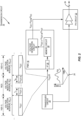
- FIG. 2 is a schematic diagram of an example transmission circuit 16 wherein a PMIC 18 and a transceiver circuit 20 are configured according to embodiments of the present disclosure to enable inter-symbol and intra-symbol voltage modulation.
- the transmission circuit 16 also includes a power amplifier circuit 22.
- the power amplifier circuit 22 is configured to amplify an RF signal 24 based on a modulated voltage Vcc, which can be an envelope tracking (ET) modulated voltage or an average power tracking (APT) modulated voltage.
- the PMIC 18 is configured to generate the modulated voltage Vcc and the transceiver circuit 20 is configured to generate the RF signal 24.
- the transceiver circuit 20 is configured to modulate the RF signal 24 onto the symbols 14(1)-14(N) in Figure 1 .
- three consecutive symbols 14(X-1), 14(X), 14(X+1) among the symbols 14(1)-14(N) (X > 1, N ⁇ X+1) are illustrated as an example.
- some of the symbols 14(X-1), 14(X), 14(X+1) may be modulated to carry the selected type of information, while some other ones of the symbols 14(X-1), 14(X), 14(X+1) may not.
- the symbol 14(X) is modulated to carry the selected type of information, and symbols 14(X-1) and 14(X+1) do not contain the selected type of information.
- the transmission circuit 16 will perform intra-symbol voltage modulation during the symbol 14(X) and inter-symbol voltage modulation during the symbols 14(X-1) and 14(X+1).
- intra-symbol voltage modulation means that the PMIC 18 can change the modulated voltage Vcc multiple times during the symbol 14(X).
- inter-symbol voltage modulation means that the PMIC 18 does not change the modulated voltage V CC during any of the symbols 14(X-1) and 14(X+1).
- the PMIC 18 can still change the modulated voltage Vcc between the symbols 14(X-1) and 14(X+1).
- the modulated voltage Vcc in the symbol 14(X-1) can be identical to or different from the modulated voltage Vcc in the symbol 14(X+1).
- Each of the voltage modulation intervals S X-1 , Sx, Sx+i correspond to a respective one of the symbols 14(X-1), 14(X), 14(X+1).
- the voltage modulation intervals S X-1 , Sx, S X+1 represent three consecutive voltage modulation intervals among any number of voltage modulation intervals, so chosen for the sole purpose of illustration. Understandably, the voltage modulation interval S X-1 is an immediately preceding voltage modulation interval of the voltage modulation interval Sx, the voltage modulation interval Sx is an immediately preceding voltage modulation interval of the voltage modulation interval S X+1 , and so on.
- the PMIC 18 includes an inter-chip interface 26, a memory circuit 28, and a voltage generation circuit 30.
- the inter-chip interface 26 can be a multiwire interface, such as an RF front-end (RFFE) interface, that is coupled to the transceiver circuit 20.
- the transceiver circuit 20 is configured to generate the RF signal 24 with a time-variant power envelope P(t) that can increase or decrease multiple times during each of the symbols 14(X-1), 14(X), 14(X+1).
- the PMIC 18 can generate multiple modulated voltages V CC1 -V CCN during the voltage modulation interval Sx to better track (increase or decrease) the time-variant power envelope P(t) on an intra-symbol basis to help avoid potential distortion (e.g., amplitude clipping) to the RF signal 24 when the RF signal 24 is amplified by the power amplifier circuit 22.
- Common elements between Figures 2 and 3A-3B are shown therein with common element numbers and will not be re-described herein.
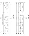
- the transceiver circuit 20 can divide the voltage modulation intervals Sx equally such that each of the modulation subintervals T 1 -T N will have an identical duration.
- the transceiver circuit 20 can divide the voltage modulation interval Sx unequally such that each of the modulation subintervals T 1 -T N will have different durations. For example, the transceiver circuit 20 can make any of the modulation subintervals T 1 -T N longer if a variation of the modulated voltage Vcc exceeds a preset threshold between adjacent ones of the modulation subintervals T 1 -T N , or make any of the modulation subintervals T 1 -T N shorter if the modulated voltage Vcc remains unchanged or the variation of the modulated voltage Vcc is below the preset threshold in between the adjacent ones of the modulation subintervals T 1 -T N .
- the transceiver circuit 20 is also configured to set the voltage targets V TGT-1 -V TGT-N for each of the modulation subintervals T 1 -T N based on the time-variant power envelope P(t) of the RF signal 24.
- the transceiver circuit 20 can set a respective one of the voltage targets V TGT-1 -V TGT-N for a respective one of the modulation subintervals T 1 -T N based on a maximum of the time-variant power envelope P(t) during the respective one of the modulation subintervals T 1 -T N .
- the transceiver circuit 20 is configured to write the voltage targets V TGT - 1 -V TGT - N , in association with the modulation subintervals T 1 -T N , into the memory circuit 28 via the inter-chip interface 26.
- the transceiver circuit 20 may write the voltage targets V TGT-1 -V TGT-N associated with the voltage modulation interval Sx prior to a start of the voltage modulation interval Sx.
- the transceiver circuit 20 will write the voltage targets V TGT-1 -V TGT-N associated with the voltage modulation interval Sx during an immediately preceding one of the voltage modulation intervals S X-1 , Sx, S X+1 .
- the transceiver circuit 20 will write the voltage targets V TGT-1 -V TGT-N associated with the voltage modulation interval Sx during the voltage modulation interval Sx-i.
- the voltage generation circuit 30 retrieves the voltage targets V TGT-1 -V TGT-N , in association with the modulation subintervals T 1 -T N , from the memory circuit 28. Accordingly, the voltage generation circuit 30 can generate the modulated voltages V CC-1 -V CC-N during the modulation subintervals T 1 -T N based on the voltage targets V TGT-1 -V TGT-N , respectively.
- Figure 4 is a block diagram providing an example illustration as to how the PMIC 18 in Figure 2 can perform intra-symbol voltage modulation during the voltage modulation interval Sx. Common elements between Figures 2 and 4 are shown therein with common element numbers and will not be re-described herein.
- the voltage generation circuit 30 is configured to determine multiple starts T START-1 -T START-N of the modulation subintervals T 1 -T N , respectively.
- the voltage generation circuit 30 can receive the start T START-1 -T START-N of the modulation subintervals T 1 -T N from the transceiver circuit 20 together with or separately from the voltage targets V TGT-1 -V TGT-N . Accordingly, the voltage generation circuit 30 can generate each of the modulated voltages V CC-1 -V CC-N no later than a respective one of the determined start T START-1 -T START-N of the voltage modulation subintervals T 1 -T N .
- the voltage generation circuit 30 is configured to determine whether each of the modulated voltages V CC-1 -V CC-N is set to increase or decrease during a respective one of the modulation subintervals T 1 -T N . If any of the modulated voltages V CC-1 -V CC-N is set to increase during the respective one of the modulation subintervals T 1 -T N , the voltage generation circuit 30 may start transitioning to the respective one the modulated voltages V CC-1 -V CC-N prior to the respective start T START-1 -T START-N of the respective one of the modulation subintervals T 1 -T N .
- the voltage generation circuit 30 determines that the modulated voltages V CC-1 and V CC-3 are set to increase during the modulation subintervals T 1 and T 3 , respectively. Accordingly, the voltage generation circuit 30 will start transitioning to the modulated voltages V CC-1 and V CC-3 with a timing advance T a prior to the respective starts T START-1 and T START-3 of the modulation subintervals T 1 and T 3 . By starting the transition with the timing advance T a , the voltage generation circuit 30 can ensure that the modulated voltages V CC-1 and V CC-3 can be ramped up to desired levels in time to help avoid amplitude clipping in the RF signal 24.
- the voltage generation circuit 30 may start transitioning to the respective one the modulated voltages V CC-1 -V CC-N at the respective start T START-1 -T START-N of the respective one of the modulation subintervals T 1 -T N .
- the voltage generation circuit 30 determines that the modulated voltages V CC-2 and V CC-N are set to decrease during the modulation subintervals T 2 and T N , respectively. Accordingly, the voltage generation circuit 30 will start transitioning to the modulated voltages V CC-2 and V CC-N right at the respective starts T START-2 and T START-N of the modulation subintervals T 2 and T N .
- Figure 5 is a schematic diagram of the voltage generation circuit 30 configured according to an embodiment of the present disclosure. Common elements between Figures 2 and 5 are shown therein with common element numbers and will not be re-described herein.
- the voltage generation circuit 30 includes a current modulation circuit 32, a voltage modulation circuit 34, and a control circuit 36.
- the current modulation circuit 32 includes a multi-level charge pump (MCP) 38 and a power inductor 40.
- MCP multi-level charge pump
- the MCP 38 is configured to generate multiple low-frequency voltages V DC-1 -V DCN , each as a function of a battery voltage V BAT , during the modulation subintervals T 1 -T N , respectively.
- the power inductor 40 is configured to induce multiple low frequency currents I DC1 -I DCN based on the low-frequency voltages V DC-1 -V DCN , respectively.
- the voltage modulation circuit 34 includes a voltage amplifier 42, an offset capacitor C OFF , and a bypass switch S BYP .
- the voltage amplifier 42 is configured to generate multiple modulated initial voltages V AMP1 -V AMPN based on the voltage targets V TGT-1 -V TGT-N in the modulation subintervals T 1 -T N , respectively.
- the offset capacitor C OFF is modulated by the low frequency currents I DC1 -I DCN to multiple offset voltages V OFF1 -V OFFN in the modulation subintervals T 1 -T N , respectively.
- Each of the offset voltages V OFF1 -V OFFN will raise a respective one of the modulated initial voltages V AMP1 -V AMPN to a respective one of the modulated voltages V CC1 -V CCN .
- the offset voltages V OFF1 -V OFFN can be modulated by the low frequency currents I DC1 -I DCN to raise the modulated initial voltages V AMP1 -V AMPN to the modulated voltages V CC1 -V CCN .
- U.S. Patent Application Number 17/946,224 entitled "MULTI-VOLTAGE GENERATION CIRCUIT.”
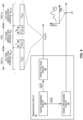
- Figure 6 is a schematic diagram illustrating the transceiver circuit 20 in Figure 2 configured to enable inter-symbol and intra-symbol voltage modulation. Common elements between Figures 2 and 6 are shown therein with common element numbers and will not be re-described herein.
- the transceiver circuit 20 includes a digital baseband circuit 44, a signal processing circuit 46, and a target voltage circuit 48.
- the digital baseband circuit 44 is configured to generate an input vector b MOD modulated in the symbols 14(X-1), 14(X), 14(X+1).
- the symbol 14(X) is modulated to include the selected type of information, while the symbols 14(X-1) and 14(X+1) are not.
- the digital baseband circuit 44 may determine which of the symbols 14(X-1), 14(X), 14(X+1) will be modulated with the selected type of information based on system configuration. For example, in a 5G or 5G-NR system, the exact symbol location of the selected type of information can be predefined in a standard, such as a third-generation partnership project (3GPP) standard.
- 3GPP third-generation partnership project
- the signal processing circuit 46 which may include digital-to-analog converter (DAC) and frequency converter (not shown), is configured to generate the RF signal 24 from the input vector b MOD and provide the RF signal 24 to the power amplifier circuit 22 in Figure 2 .
- DAC digital-to-analog converter
- frequency converter not shown
- the target voltage circuit 48 may include an internal memory and an internal processor, which are not shown herein for the sake of simplicity.
- the internal memory which can be any type of memory, may store a target voltage lookup table (LUT) that correlates a time-variant amplitude of the input vector b MOD with various levels of voltage targets.
- the internal memory may also store the exact symbol location of the selected type of information such that the internal processor (e.g., a digital signal processor) in the target voltage circuit 48 can determine whether the selected type of information is modulated in any of the symbols 14(X-1), 14(X), 14(X+1).
- the digital baseband circuit 44 may provide an indication to the target voltage circuit 48 as to which of the symbols 14(X-1), 14(X), 14(X+1) is modulated with the selected type of information.
- the target voltage circuit 48 is configured to determine the voltage modulation intervals S X-1 , Sx, Sx+i that correspond respectively to the symbols 14(X-1), 14(X), 14(X+1). In one embodiment, the internal processor of the target voltage circuit 48 determines that the symbol 14(X) is modulated to include the selected type of information. Accordingly, the internal processor in the target voltage circuit 48 divides the voltage modulation interval Sx into the voltage modulation subintervals T 1 -T N and uses the target voltage LUT to generate the voltage targets V TGT-1 -V TGT-N for the voltage modulation subintervals T 1 -T N , respectively.
- the target voltage LUT may store the various levels of voltage targets in digital formats.
- the target voltage circuit 48 may also include an internal DAC (not shown) to convert the voltage targets V TGT-1 -V TGT-N or the single voltage target V TGT into respective analog formats in the target voltage indications VTGT(i).
- the transmission circuit 16 of Figure 2 can be configured to enable inter-symbol and intra-symbol voltage modulation based on a process.
- Figure 7 is a flowchart of an example process 200 for enabling inter-symbol and intra-symbol voltage modulation according to embodiments of the present disclosure.
- the digital baseband circuit 44 is configured to generate an input vector b MOD modulated to include the selected type of information in one or more (e.g., symbol 14(X)) of the symbols 14(X-1), 14(X), 14(X+1) (step 202).
- the target voltage circuit 48 is configured to determine the voltage modulation intervals S X-1 , Sx, Sx+i corresponding to the symbols 14(X-1), 14(X), 14(X+1) (step 204).
- the target voltage circuit 48 then divides a respective one (e.g., voltage modulation interval Sx) of the voltage modulation intervals S X-1 , Sx, Sx+i into the voltage modulation subintervals T 1 -T N , each of the voltage modulation subintervals includes a respective one of the voltage targets V TGT-1 -V TGT-N when the target voltage circuit 48 determines that a corresponding one (e.g., symbol 14(X)) of the symbols 14(X-1), 14(X), 14(X+1) includes the selected type of information (step 206).
- a corresponding one e.g., symbol 14(X)
- the voltage generation circuit 30 will then generate the modulated voltages V CC1 -V CCN in the voltage modulation subintervals T 1 -T N based on the voltage targets V TGT - 1 -V TGT - N , respectively (step 210).
- a transceiver circuit is configured to determine a voltage target(s) for generating a modulated voltage(s) to amplify a radio frequency (RF) signal modulated in multiple symbols. Specifically, the transceiver circuit will generate multiple voltage targets for any of the symbols to thereby enable intra-symbol voltage modulation when the respective symbol is modulated to carry a selected type of information or generate a single voltage target for any of the symbols to thereby enable inter-symbol voltage modulation when the respective symbol lacks the selected type of information.
- RF radio frequency
- the modulated voltage can be timely adapted to closely track a time-variant power envelope of the RF signal to thereby avoid potential distortion and protect critical information in the RF signal.
Landscapes
- Engineering & Computer Science (AREA)
- Power Engineering (AREA)
- Computer Networks & Wireless Communication (AREA)
- Signal Processing (AREA)
- Transmitters (AREA)
Abstract
Description
- This application claims the benefit of
U.S. provisional patent application serial number 63/255,659 filed on October 14, 2021 U.S. provisional patent application serial number 63/255,656 filed on October 14, 2021 - The technology of the disclosure relates generally to inter-symbol and intra-symbol voltage modulation.
- Fifth generation (5G) new radio (NR) (5G-NR) has been widely regarded as the next generation of wireless communication technology beyond the current third generation (3G) and fourth generation (4G) technologies. In this regard, a wireless communication device capable of supporting the 5G-NR wireless communication technology is expected to achieve higher data rates, improved coverage range, enhanced signaling efficiency, and reduced latency.
- Downlink and uplink transmissions in a 5G-NR system are widely based on orthogonal frequency division multiplexing (OFDM) technology. In an OFDM based system, physical radio resources are divided into a number of subcarriers in a frequency domain and a number of OFDM symbols in a time domain. The subcarriers are orthogonally separated from each other by a subcarrier spacing (SCS). The OFDM symbols are separated from each other by a cyclic prefix (CP), which acts as a guard band to help overcome inter-symbol interference (ISI) between the OFDM symbols.
- A radio frequency (RF) signal communicated in the OFDM based system is often modulated into multiple subcarriers in the frequency domain and multiple OFDM symbols in the time domain. The multiple subcarriers occupied by the RF signal collectively define a modulation bandwidth of the RF signal. The multiple OFDM symbols, on the other hand, define multiple time intervals during which the RF signal is communicated. In the 5G-NR system, the RF signal is typically modulated with a high modulation bandwidth in excess of 200 MHz.
- The duration of an OFDM symbol depends on the SCS and the modulation bandwidth. The table below (Table 1) provides some OFDM symbol durations, as defined by 3G partnership project (3GPP) standards for various SCSs and modulation bandwidths. Notably, the higher the modulation bandwidth is, the shorter the OFDM symbol duration will be. For example, when the SCS is 120 KHz and the modulation bandwidth is 400 MHz, the OFDM symbol duration is 8.93 µs.
Table 1 SCS (KHz) CP (µs) OFDM Symbol Duration (µs) Modulation Bandwidth (MHz) 15 4.69 71.43 50 30 2.34 35.71 100 60 1.17 17.86 200 120 0.59 8.93 400 - In a 5G-NR system, the RF signal can be modulated with a time-variant power that changes from one OFDM symbol to another. In this regard, a power amplifier circuit(s) is required to amplify the RF signal to a certain power level within each OFDM symbol duration. Such inter-symbol power variation creates a unique challenge for a power management integrated circuit (PMIC) because the PMIC must be able to adapt a modulated voltage supplied to the power amplifier circuit within the CP of each OFDM symbol to help avoid distortion (e.g., amplitude clipping) in the RF signal.
- Particular aspects are set out in the appended independent claims. Various optional embodiments are set out in the dependent claims.
- Embodiments of the disclosure relate to a circuit and method for inter-symbol and intra-symbol voltage modulation. Herein, a transceiver circuit is configured to determine a voltage target(s) and provide the voltage target(s) to a power management integrated circuit (PMIC) for generating a modulated voltage(s) to amplify a radio frequency (RF) signal modulated in multiple symbols. Specifically, the transceiver circuit will generate multiple voltage targets for any of the symbols to thereby enable intra-symbol voltage modulation when the respective symbol is modulated to carry a selected type of information (e.g., control information). In contrast, the transceiver circuit will generate a single voltage target for any of the symbols to thereby enable inter-symbol voltage modulation when the respective symbol is not modulated to carry the selected type of information. By dynamically performing inter-symbol and intra-symbol voltage modulation based on the type of information carried in a symbol(s), the modulated voltage can be timely adapted to closely track a time-variant power envelope of the RF signal to thereby avoid potential distortion (e.g., amplitude clipping) and protect critical information in the RF signal.
- In one aspect, a transceiver circuit is provided. The transceiver circuit includes a digital baseband circuit. The digital baseband circuit is configured to generate an input vector including a selected type of information modulated in one or more of multiple symbols. The transceiver circuit also includes a target voltage circuit. The target voltage circuit is configured to determine multiple voltage modulation intervals corresponding to the multiple symbols, respectively. The target voltage circuit is also configured to divide a respective one of the multiple voltage modulation intervals into multiple voltage modulation subintervals each including a respective one of multiple voltage targets when a corresponding one of the multiple symbols includes the selected type of information. The target voltage circuit is also configured to generate a respective one of multiple target voltage indications including the multiple voltage targets.
- In another aspect, a transmission circuit is provided. The transmission circuit includes a transceiver circuit. The transceiver circuit includes a digital baseband circuit. The digital baseband circuit is configured to generate an input vector including a selected type of information modulated in one or more of multiple symbols. The transceiver circuit also includes a target voltage circuit. The target voltage circuit is configured to determine multiple voltage modulation intervals corresponding to the multiple symbols, respectively. The target voltage circuit is also configured to divide a respective one of the multiple voltage modulation intervals into multiple voltage modulation subintervals each including a respective one of multiple voltage targets when a corresponding one of the multiple symbols includes the selected type of information. The target voltage circuit is also configured to generate a respective one of multiple target voltage indications including the multiple voltage targets. The transmission circuit also includes a PMIC. The PMIC includes a voltage generation circuit. The voltage generation circuit is configured to receive the multiple target voltage indications from the transceiver circuit. The voltage generation circuit is also configured to generate multiple modulated voltages in the multiple voltage modulation subintervals based on the multiple voltage targets, respectively.
- In another aspect, a method for enabling inter-symbol and intra-symbol voltage modulation is provided. The method includes generating an input vector including a selected type of information modulated in one or more of multiple symbols. The method also includes determining multiple voltage modulation intervals corresponding to the multiple symbols, respectively. The method also includes dividing a respective one of the multiple voltage modulation intervals into multiple voltage modulation subintervals each including a respective one of multiple of voltage targets when a corresponding one of the multiple symbols includes the selected type of information. The method also includes generating a respective one of multiple target voltage indications including the multiple voltage targets. The method also includes generating multiple modulated voltages in the multiple voltage modulation subintervals based on the multiple voltage targets, respectively.
- Those skilled in the art will appreciate the scope of the present disclosure and realize additional aspects thereof after reading the following detailed description of the preferred embodiments in association with the accompanying drawing figures.
- The accompanying drawing figures incorporated in and forming a part of this specification illustrate several aspects of the disclosure, and together with the description serve to explain the principles of the disclosure.
-
Figure 1 illustrates example time slot(s) and a mini time slot(s) as widely supported in a fifth generation (5G) or a 5G new-radio (5G-NR) system; -
Figure 2 is a schematic diagram of an example transmission circuit wherein a power management integrated circuit (PMIC) and a transceiver circuit are configured according to embodiments of the present disclosure to enable inter-symbol and intra-symbol voltage modulation; -
Figures 3A and 3B are block diagrams providing example illustrations of a target voltage indication generated by the transceiver circuit inFigure 2 to cause the PMIC to perform the intra-symbol voltage modulation; -
Figure 4 is a block diagram providing an example illustration as to how the PMIC inFigure 2 can perform the intra-symbol voltage modulation; -
Figure 5 is a schematic diagram of an example voltage modulation circuit, which can be provided in the PMIC inFigure 2 to perform inter-symbol and intra-symbol voltage modulation during the voltage modulation interval(s); -
Figure 6 is a schematic diagram illustrating the transceiver circuit inFigure 2 configured to enable inter-symbol and intra-symbol voltage modulation; and -
Figure 7 is a flowchart of an example process for enabling inter-symbol and intra-symbol voltage modulation according to embodiments of the present disclosure. - The embodiments set forth below represent the necessary information to enable those skilled in the art to practice the embodiments and illustrate the best mode of practicing the embodiments. Upon reading the following description in light of the accompanying drawing figures, those skilled in the art will understand the concepts of the disclosure and will recognize applications of these concepts not particularly addressed herein. It should be understood that these concepts and applications fall within the scope of the disclosure and the accompanying claims.
- It will be understood that, although the terms first, second, etc. may be used herein to describe various elements, these elements should not be limited by these terms. These terms are only used to distinguish one element from another. For example, a first element could be termed a second element, and, similarly, a second element could be termed a first element, without departing from the scope of the present disclosure. As used herein, the term "and/or" includes any and all combinations of one or more of the associated listed items.
- It will be understood that when an element such as a layer, region, or substrate is referred to as being "on" or extending "onto" another element, it can be directly on or extend directly onto the other element or intervening elements may also be present. In contrast, when an element is referred to as being "directly on" or extending "directly onto" another element, there are no intervening elements present. Likewise, it will be understood that when an element such as a layer, region, or substrate is referred to as being "over" or extending "over" another element, it can be directly over or extend directly over the other element or intervening elements may also be present. In contrast, when an element is referred to as being "directly over" or extending "directly over" another element, there are no intervening elements present. It will also be understood that when an element is referred to as being "connected" or "coupled" to another element, it can be directly connected or coupled to the other element or intervening elements may be present. In contrast, when an element is referred to as being "directly connected" or "directly coupled" to another element, there are no intervening elements present.
- Relative terms such as "below" or "above" or "upper" or "lower" or "horizontal" or "vertical" may be used herein to describe a relationship of one element, layer, or region to another element, layer, or region as illustrated in the Figures. It will be understood that these terms and those discussed above are intended to encompass different orientations of the device in addition to the orientation depicted in the Figures.
- The terminology used herein is for the purpose of describing particular embodiments only and is not intended to be limiting of the disclosure. As used herein, the singular forms "a," "an," and "the" are intended to include the plural forms as well, unless the context clearly indicates otherwise. It will be further understood that the terms "comprises," "comprising," "includes," and/or "including" when used herein specify the presence of stated features, integers, steps, operations, elements, and/or components, but do not preclude the presence or addition of one or more other features, integers, steps, operations, elements, components, and/or groups thereof.
- Unless otherwise defined, all terms (including technical and scientific terms) used herein have the same meaning as commonly understood by one of ordinary skill in the art to which this disclosure belongs. It will be further understood that terms used herein should be interpreted as having a meaning that is consistent with their meaning in the context of this specification and the relevant art and will not be interpreted in an idealized or overly formal sense unless expressly so defined herein.
- Embodiments of the disclosure relate to circuit and method for inter-symbol and intra-symbol voltage modulation. Herein, a transceiver circuit is configured to determine a voltage target(s) and provide the voltage target(s) to a power management integrated circuit (PMIC) for generating a modulated voltage(s) to amplify a radio frequency (RF) signal modulated in multiple symbols. Specifically, the transceiver circuit will generate multiple voltage targets for any of the symbols to thereby enable intra-symbol voltage modulation when the respective symbol is modulated to carry a selected type of information (e.g., control information). In contrast, the transceiver circuit will generate a single voltage target for any of the symbols to thereby enable inter-symbol voltage modulation when the respective symbol is not modulated to carry the selected type of information. By dynamically performing inter-symbol and intra-symbol voltage modulation based on the type of information carried in a symbol(s), the modulated voltage can be timely adapted to closely track a time-variant power envelope of the RF signal to thereby avoid potential distortion (e.g., amplitude clipping) and protect critical information in the RF signal.
- Before discussing inter-symbol and intra-symbol voltage modulation of the present disclosure, starting at
Figure 2 , an overview of orthogonal frequency division multiplexing (OFDM) symbols, which can be used to define durations of voltage modulation intervals, is first provided with reference toFigure 1 . -
Figure 1 illustrates example time slot(s) 10 and a pair of mini time slots 12(1)-12(2) as widely supported in a fifth generation (5G) and 5G new-generation (5G-NR) system. The time slot(s) 10, which can represent any one or more of multiple continuous time slots, includes multiple symbols 14(1)-14(N), such as OFDM symbols. The mini time slots 12(1)-12(2) can each include at least two of the symbols 14(1)-14(N). In the example shown inFigure 1 , each of the mini time slots 12(1)-12(2) includes four of the symbols 14(1)-14(N). As previously shown in Table 1, each of the symbols 14(1)-14(N) has a symbol duration that depends on the subcarrier spacing (SCS). Once the SCS is chosen, the duration and the CP of each of the symbols 14(1)-14(N) are set accordingly. - The symbols 14(1)-14(N) in the time slot(s) 10 can be modulated based on any type of modulation and coding scheme (MCS) to carry various types of information. For example, some of the symbols 14(1)-14(N) can be modulated to carry downlink/uplink control information, some of the symbols 14(1)-14(N) can be modulated to carry downlink/uplink data payload, and yet some of the symbols 14(1)-14(N) can be empty (e.g., not bearing any information). Among the symbols 14(1)-14(N), those symbols that are modulated to carry a selected type of information are of special importance in the context of the present disclosure.
- Herein, the selected type of information may include information related to physical downlink control channel (PDCCH), physical uplink control channel (PUCCH), physical downlink shared channel (PDSCH), and/or physical uplink shared channel (PUSCH). In a non-limiting example, the selected type of information can be a sounding reference signal (SRS), a demodulation reference signal (DMRS), and so on. As described in detail below, whether the selected type of information is present or absent in any of the symbols 14(1)-14(N) is a determining factor for intra-symbol or inter-symbol voltage modulation.
-
Figure 2 is a schematic diagram of anexample transmission circuit 16 wherein aPMIC 18 and atransceiver circuit 20 are configured according to embodiments of the present disclosure to enable inter-symbol and intra-symbol voltage modulation. Thetransmission circuit 16 also includes apower amplifier circuit 22. Thepower amplifier circuit 22 is configured to amplify anRF signal 24 based on a modulated voltage Vcc, which can be an envelope tracking (ET) modulated voltage or an average power tracking (APT) modulated voltage. ThePMIC 18 is configured to generate the modulated voltage Vcc and thetransceiver circuit 20 is configured to generate theRF signal 24. - The
transceiver circuit 20 is configured to modulate theRF signal 24 onto the symbols 14(1)-14(N) inFigure 1 . Herein, three consecutive symbols 14(X-1), 14(X), 14(X+1) among the symbols 14(1)-14(N) (X > 1, N ≥ X+1) are illustrated as an example. As described above, some of the symbols 14(X-1), 14(X), 14(X+1) may be modulated to carry the selected type of information, while some other ones of the symbols 14(X-1), 14(X), 14(X+1) may not. As an example, it is assumed that the symbol 14(X) is modulated to carry the selected type of information, and symbols 14(X-1) and 14(X+1) do not contain the selected type of information. In this regard, as further described below, thetransmission circuit 16 will perform intra-symbol voltage modulation during the symbol 14(X) and inter-symbol voltage modulation during the symbols 14(X-1) and 14(X+1). - Herein, intra-symbol voltage modulation means that the
PMIC 18 can change the modulated voltage Vcc multiple times during the symbol 14(X). In contrast, inter-symbol voltage modulation means that thePMIC 18 does not change the modulated voltage VCC during any of the symbols 14(X-1) and 14(X+1). However, with inter-symbol voltage modulation, thePMIC 18 can still change the modulated voltage Vcc between the symbols 14(X-1) and 14(X+1). In other words, the modulated voltage Vcc in the symbol 14(X-1) can be identical to or different from the modulated voltage Vcc in the symbol 14(X+1). - In an embodiment, the
transceiver circuit 20 is configured to generate multiple target voltage indications VTGT(i) (i = X-1, X, X+1) in multiple voltage modulation intervals SX-1, Sx, SX+1, respectively. Each of the voltage modulation intervals SX-1, Sx, Sx+i correspond to a respective one of the symbols 14(X-1), 14(X), 14(X+1). In other words, there exists a one-to-one relationship between the voltage modulation intervals SX-1, Sx, SX+1 and the symbols 14(X-1), 14(X), 14(X+1). Notably, the voltage modulation intervals SX-1, Sx, SX+1 represent three consecutive voltage modulation intervals among any number of voltage modulation intervals, so chosen for the sole purpose of illustration. Understandably, the voltage modulation interval SX-1 is an immediately preceding voltage modulation interval of the voltage modulation interval Sx, the voltage modulation interval Sx is an immediately preceding voltage modulation interval of the voltage modulation interval SX+1, and so on. - According to an embodiment of the present disclosure, the
PMIC 18 includes aninter-chip interface 26, amemory circuit 28, and avoltage generation circuit 30. In a non-limiting example, theinter-chip interface 26 can be a multiwire interface, such as an RF front-end (RFFE) interface, that is coupled to thetransceiver circuit 20. Thetransceiver circuit 20 is configured to provide a respective target voltage indication VTGT(i) (i = X-1, X, X+1, and so on) for each of the voltage modulation intervals SX-1, Sx, Sx+i. - Specifically, to enable to
PMIC 18 to perform inter-symbol voltage modulation, thetransceiver circuit 20 is configured to determine and provide a single voltage target VTGT to thePMIC 18 in the target voltage indications VTGT(i) (i = X-1, X+1). Accordingly, thePMIC 18 will generate the modulated voltage Vcc during the voltage modulation intervals SX-1, Sx+i based on the respective voltage target VTGT received in the target voltage indications VTGT(i) (i = X-1, X+1). - Notably, the
transceiver circuit 20 is configured to generate theRF signal 24 with a time-variant power envelope P(t) that can increase or decrease multiple times during each of the symbols 14(X-1), 14(X), 14(X+1). In this regard, since the symbol 14(X) includes the selected type of information, it is desirable that thePMIC 18 can generate multiple modulated voltages VCC1-VCCN during the voltage modulation interval Sx to better track (increase or decrease) the time-variant power envelope P(t) on an intra-symbol basis to help avoid potential distortion (e.g., amplitude clipping) to theRF signal 24 when theRF signal 24 is amplified by thepower amplifier circuit 22. -
Figures 3A and 3B are block diagrams providing example illustrations of the target voltage indication VTGT(i) (i = X) generated by thetransceiver circuit 20 inFigure 2 to cause thePMIC 18 to perform the intra-symbol voltage modulation during the voltage modulation interval Sx. Common elements betweenFigures 2 and3A-3B are shown therein with common element numbers and will not be re-described herein. - In one embodiment, as illustrated in
Figure 3A , thetransceiver circuit 20 can divide the voltage modulation intervals Sx equally such that each of the modulation subintervals T1-TN will have an identical duration. - In another embodiment, as illustrated in
Figure 3B , thetransceiver circuit 20 can divide the voltage modulation interval Sx unequally such that each of the modulation subintervals T1-TN will have different durations. For example, thetransceiver circuit 20 can make any of the modulation subintervals T1-TN longer if a variation of the modulated voltage Vcc exceeds a preset threshold between adjacent ones of the modulation subintervals T1-TN, or make any of the modulation subintervals T1-TN shorter if the modulated voltage Vcc remains unchanged or the variation of the modulated voltage Vcc is below the preset threshold in between the adjacent ones of the modulation subintervals T1-TN. - With reference back to
Figure 2 , thetransceiver circuit 20 is also configured to set the voltage targets VTGT-1-VTGT-N for each of the modulation subintervals T1-TN based on the time-variant power envelope P(t) of theRF signal 24. In a non-limiting example, thetransceiver circuit 20 can set a respective one of the voltage targets VTGT-1-VTGT-N for a respective one of the modulation subintervals T1-TN based on a maximum of the time-variant power envelope P(t) during the respective one of the modulation subintervals T1-TN. - The
transceiver circuit 20 is configured to write the voltage targets VTGT-1-VTGT-N, in association with the modulation subintervals T1-TN, into thememory circuit 28 via theinter-chip interface 26. In one embodiment, thetransceiver circuit 20 may write the voltage targets VTGT-1-VTGT-N associated with the voltage modulation interval Sx prior to a start of the voltage modulation interval Sx. In particular implementations, thetransceiver circuit 20 will write the voltage targets VTGT-1-VTGT-N associated with the voltage modulation interval Sx during an immediately preceding one of the voltage modulation intervals SX-1, Sx, SX+1. For example, thetransceiver circuit 20 will write the voltage targets VTGT-1-VTGT-N associated with the voltage modulation interval Sx during the voltage modulation interval Sx-i. - Prior to the voltage modulation interval Sx, the
voltage generation circuit 30 retrieves the voltage targets VTGT-1-VTGT-N, in association with the modulation subintervals T1-TN, from thememory circuit 28. Accordingly, thevoltage generation circuit 30 can generate the modulated voltages VCC-1-VCC-N during the modulation subintervals T1-TN based on the voltage targets VTGT-1-VTGT-N, respectively. -
Figure 4 is a block diagram providing an example illustration as to how thePMIC 18 inFigure 2 can perform intra-symbol voltage modulation during the voltage modulation interval Sx. Common elements betweenFigures 2 and4 are shown therein with common element numbers and will not be re-described herein. - The
voltage generation circuit 30 is configured to determine multiple starts TSTART-1-TSTART-N of the modulation subintervals T1-TN, respectively. In a non-limiting example, thevoltage generation circuit 30 can receive the start TSTART-1-TSTART-N of the modulation subintervals T1-TN from thetransceiver circuit 20 together with or separately from the voltage targets VTGT-1-VTGT-N. Accordingly, thevoltage generation circuit 30 can generate each of the modulated voltages VCC-1-VCC-N no later than a respective one of the determined start TSTART-1-TSTART-N of the voltage modulation subintervals T1-TN. - According to an embodiment of the present disclosure, the
voltage generation circuit 30 is configured to determine whether each of the modulated voltages VCC-1-VCC-N is set to increase or decrease during a respective one of the modulation subintervals T1-TN. If any of the modulated voltages VCC-1-VCC-N is set to increase during the respective one of the modulation subintervals T1-TN, thevoltage generation circuit 30 may start transitioning to the respective one the modulated voltages VCC-1-VCC-N prior to the respective start TSTART-1-TSTART-N of the respective one of the modulation subintervals T1-TN. For example, thevoltage generation circuit 30 determines that the modulated voltages VCC-1 and VCC-3 are set to increase during the modulation subintervals T1 and T3, respectively. Accordingly, thevoltage generation circuit 30 will start transitioning to the modulated voltages VCC-1 and VCC-3 with a timing advance Ta prior to the respective starts TSTART-1 and TSTART-3 of the modulation subintervals T1 and T3. By starting the transition with the timing advance Ta, thevoltage generation circuit 30 can ensure that the modulated voltages VCC-1 and VCC-3 can be ramped up to desired levels in time to help avoid amplitude clipping in theRF signal 24. - In contrast, if any of the modulated voltages VCC-1-VCC-N is set to increase, or remain unchanged, during the respective one of the modulation subintervals T1-TN, the
voltage generation circuit 30 may start transitioning to the respective one the modulated voltages VCC-1-VCC-N at the respective start TSTART-1-TSTART-N of the respective one of the modulation subintervals T1-TN. For example, thevoltage generation circuit 30 determines that the modulated voltages VCC-2 and VCC-N are set to decrease during the modulation subintervals T2 and TN, respectively. Accordingly, thevoltage generation circuit 30 will start transitioning to the modulated voltages VCC-2 and VCC-N right at the respective starts TSTART-2 and TSTART-N of the modulation subintervals T2 and TN. -
Figure 5 is a schematic diagram of thevoltage generation circuit 30 configured according to an embodiment of the present disclosure. Common elements betweenFigures 2 and5 are shown therein with common element numbers and will not be re-described herein. - Herein, the
voltage generation circuit 30 includes acurrent modulation circuit 32, avoltage modulation circuit 34, and acontrol circuit 36. Thecurrent modulation circuit 32 includes a multi-level charge pump (MCP) 38 and apower inductor 40. During the voltage modulation interval Sx, theMCP 38 is configured to generate multiple low-frequency voltages VDC-1-VDCN, each as a function of a battery voltage VBAT, during the modulation subintervals T1-TN, respectively. Accordingly, in the voltage modulation interval Sx, thepower inductor 40 is configured to induce multiple low frequency currents IDC1-IDCN based on the low-frequency voltages VDC-1-VDCN, respectively. - The
voltage modulation circuit 34 includes avoltage amplifier 42, an offset capacitor COFF, and a bypass switch SBYP. Thevoltage amplifier 42 is configured to generate multiple modulated initial voltages VAMP1-VAMPN based on the voltage targets VTGT-1-VTGT-N in the modulation subintervals T1-TN, respectively. The offset capacitor COFF is modulated by the low frequency currents IDC1-IDCN to multiple offset voltages VOFF1-VOFFN in the modulation subintervals T1-TN, respectively. Each of the offset voltages VOFF1-VOFFN will raise a respective one of the modulated initial voltages VAMP1-VAMPN to a respective one of the modulated voltages VCC1-VCCN. For specific example as to how the offset voltages VOFF1-VOFFN can be modulated by the low frequency currents IDC1-IDCN to raise the modulated initial voltages VAMP1-VAMPN to the modulated voltages VCC1-VCCN, please refer toU.S. Patent Application Number 17/946,224 , entitled "MULTI-VOLTAGE GENERATION CIRCUIT." -
Figure 6 is a schematic diagram illustrating thetransceiver circuit 20 inFigure 2 configured to enable inter-symbol and intra-symbol voltage modulation. Common elements betweenFigures 2 and6 are shown therein with common element numbers and will not be re-described herein. - Herein, the
transceiver circuit 20 includes adigital baseband circuit 44, asignal processing circuit 46, and atarget voltage circuit 48. Thedigital baseband circuit 44 is configured to generate an input vectorbMOD modulated in the symbols 14(X-1), 14(X), 14(X+1). According to the example described above, the symbol 14(X) is modulated to include the selected type of information, while the symbols 14(X-1) and 14(X+1) are not. In an embodiment, thedigital baseband circuit 44 may determine which of the symbols 14(X-1), 14(X), 14(X+1) will be modulated with the selected type of information based on system configuration. For example, in a 5G or 5G-NR system, the exact symbol location of the selected type of information can be predefined in a standard, such as a third-generation partnership project (3GPP) standard. - The
signal processing circuit 46, which may include digital-to-analog converter (DAC) and frequency converter (not shown), is configured to generate theRF signal 24 from the input vectorbMOD and provide theRF signal 24 to thepower amplifier circuit 22 inFigure 2 . - In an embodiment, the
target voltage circuit 48 may include an internal memory and an internal processor, which are not shown herein for the sake of simplicity. The internal memory, which can be any type of memory, may store a target voltage lookup table (LUT) that correlates a time-variant amplitude of the input vectorbMOD with various levels of voltage targets. The internal memory may also store the exact symbol location of the selected type of information such that the internal processor (e.g., a digital signal processor) in thetarget voltage circuit 48 can determine whether the selected type of information is modulated in any of the symbols 14(X-1), 14(X), 14(X+1). Alternatively, thedigital baseband circuit 44 may provide an indication to thetarget voltage circuit 48 as to which of the symbols 14(X-1), 14(X), 14(X+1) is modulated with the selected type of information. - The
target voltage circuit 48 is configured to determine the voltage modulation intervals SX-1, Sx, Sx+i that correspond respectively to the symbols 14(X-1), 14(X), 14(X+1). In one embodiment, the internal processor of thetarget voltage circuit 48 determines that the symbol 14(X) is modulated to include the selected type of information. Accordingly, the internal processor in thetarget voltage circuit 48 divides the voltage modulation interval Sx into the voltage modulation subintervals T1-TN and uses the target voltage LUT to generate the voltage targets VTGT-1-VTGT-N for the voltage modulation subintervals T1-TN, respectively. In another embodiment, the internal processor in thetarget voltage circuit 48 determines that the symbols 14(X-1) and 14(X+1) are not modulated to include the selected type of information. Accordingly, the internal processor in thetarget voltage circuit 48 uses the target voltage LUT to generate the single voltage target VTGT for the voltage modulation intervals SX-1 and SX+1. Further, the internal processor in thetarget voltage circuit 48 generates the target voltage indications VTGT(i) (i = X-1, X, X+1) and provides the target voltage indications VTGT(i) to thePMIC 18 via theinter-chip interface 26. In an embodiment, the target voltage LUT may store the various levels of voltage targets in digital formats. In this regard, thetarget voltage circuit 48 may also include an internal DAC (not shown) to convert the voltage targets VTGT-1-VTGT-N or the single voltage target VTGT into respective analog formats in the target voltage indications VTGT(i). - The
transmission circuit 16 ofFigure 2 can be configured to enable inter-symbol and intra-symbol voltage modulation based on a process. In this regard,Figure 7 is a flowchart of anexample process 200 for enabling inter-symbol and intra-symbol voltage modulation according to embodiments of the present disclosure. - Herein, the
digital baseband circuit 44 is configured to generate an input vectorbMOD modulated to include the selected type of information in one or more (e.g., symbol 14(X)) of the symbols 14(X-1), 14(X), 14(X+1) (step 202). Thetarget voltage circuit 48 is configured to determine the voltage modulation intervals SX-1, Sx, Sx+i corresponding to the symbols 14(X-1), 14(X), 14(X+1) (step 204). Thetarget voltage circuit 48 then divides a respective one (e.g., voltage modulation interval Sx) of the voltage modulation intervals SX-1, Sx, Sx+i into the voltage modulation subintervals T1-TN, each of the voltage modulation subintervals includes a respective one of the voltage targets VTGT-1-VTGT-N when thetarget voltage circuit 48 determines that a corresponding one (e.g., symbol 14(X)) of the symbols 14(X-1), 14(X), 14(X+1) includes the selected type of information (step 206). Thetarget voltage circuit 48 then generates a respective one of the target voltage indications VTGT(i) (i = X-1, X, X+1) that includes the voltage targets VTGT-1-VTGT-N (step 208). Thevoltage generation circuit 30 will then generate the modulated voltages VCC1-VCCN in the voltage modulation subintervals T1-TN based on the voltage targets VTGT-1-VTGT-N, respectively (step 210). - Therefore, from one perspective, there have been described a circuit and method for inter-symbol and intra-symbol voltage method. A transceiver circuit is configured to determine a voltage target(s) for generating a modulated voltage(s) to amplify a radio frequency (RF) signal modulated in multiple symbols. Specifically, the transceiver circuit will generate multiple voltage targets for any of the symbols to thereby enable intra-symbol voltage modulation when the respective symbol is modulated to carry a selected type of information or generate a single voltage target for any of the symbols to thereby enable inter-symbol voltage modulation when the respective symbol lacks the selected type of information. By dynamically performing inter-symbol and intra-symbol voltage modulation based on the type of information carried in a symbol(s), the modulated voltage can be timely adapted to closely track a time-variant power envelope of the RF signal to thereby avoid potential distortion and protect critical information in the RF signal.
- Further examples of the present teachings are set out in the following numbered clauses:
-
Clause 1. A transceiver circuit comprising: a digital baseband circuit configured to generate an input vector comprising a selected type of information modulated in one or more of a plurality of symbols; and a target voltage circuit configured to: determine a plurality of voltage modulation intervals corresponding to the plurality of symbols, respectively; divide a respective one of the plurality of voltage modulation intervals into a plurality of voltage modulation subintervals each comprising a respective one of a plurality of voltage targets when a corresponding one of the plurality of symbols comprises the selected type of information; and generate a respective one of a plurality of target voltage indications comprising the plurality of voltage targets. -
Clause 2. The transceiver circuit ofclause 1, wherein the selected type of information comprises one or more of: physical downlink control channel (PDCCH) information, physical uplink control channel (PUCCH) information, physical downlink shared channel (PDSCH) information, and physical uplink shared channel (PUSCH) information. -
Clause 3. The transceiver circuit ofclause - Clause 4. The transceiver circuit of
clause - Clause 5. The transceiver circuit of any preceding clause, wherein the target voltage circuit is further configured to unequally divide the respective one of the plurality of voltage modulation intervals into the plurality of voltage modulation subintervals.
- Clause 6. The transceiver circuit of any preceding clause, wherein the target voltage circuit is further configured to generate the respective one of the plurality of target voltage indications comprising a single voltage target when the corresponding one of the plurality of symbols does not contain the selected type of information.
- Clause 7. The transceiver circuit of any preceding clause, further comprising a signal processing circuit configured to generate a radio frequency (RF) signal from the input vector.
- Clause 8. A transmission circuit comprising: a transceiver circuit comprising: a digital baseband circuit configured to generate an input vector comprising a selected type of information modulated in one or more of a plurality of symbols; and a target voltage circuit configured to: determine a plurality of voltage modulation intervals corresponding to the plurality of symbols, respectively; divide a respective one of the plurality of voltage modulation intervals into a plurality of voltage modulation subintervals each comprising a respective one of a plurality of voltage targets when a corresponding one of the plurality of symbols comprises the selected type of information; and generate a respective one of a plurality of target voltage indications comprising the plurality of voltage targets; and a power management integrated circuit (PMIC) comprising a voltage generation circuit configured to: receive the plurality of target voltage indications from the transceiver circuit; and generate a plurality of modulated voltages in the plurality of voltage modulation subintervals based on the plurality of voltage targets, respectively.
- Clause 9. The transmission circuit of clause 8, wherein the PMIC further comprises: an inter-chip interface coupled to the transceiver circuit to receive the plurality of target voltage indications; and a memory circuit configured to store the plurality of received target voltage indications.
-
Clause 10. The transmission circuit of clause 8 or 9, wherein the PMIC is further configured to receive the respective one of the plurality of target voltage indications corresponding to the respective one of the plurality of voltage modulation intervals during an immediately preceding one of the plurality of voltage modulation intervals. -
Clause 11. The transmission circuit ofclause 8, 9 or 10, wherein the voltage generation circuit is further configured to generate each of the plurality of modulated voltages based on the respective one of the plurality of voltage targets no later than a respective start of the respective one of the plurality of voltage modulation subintervals. -
Clause 12. The transmission circuit ofclause 11, wherein the voltage generation circuit is further configured to: generate a respective one of the plurality of modulated voltages prior to the respective start of the respective one of the plurality of voltage modulation subintervals in response to the respective one of the plurality of voltage targets indicating that the respective one of the plurality of modulated voltages will increase during the respective one of the plurality of voltage modulation subintervals; and generate the respective one of the plurality of modulated voltages at the respective start of the respective one of the plurality of voltage modulation subintervals in response to the respective one of the plurality of voltage targets indicating that the respective one of the plurality of modulated voltages will decrease during the respective one of the plurality of voltage modulation subintervals. - Clause 13. The transmission circuit of any of clauses 8 to 12, wherein the target voltage circuit is further configured to generate a single voltage target for the respective one of the plurality of voltage modulation intervals when the respective one of the plurality of symbols does not contain the selected type of information.
-
Clause 14. The transmission circuit of clause 13, wherein the voltage generation circuit is further configured to generate a single modulated voltage during the respective one of the plurality of voltage modulation intervals based on the single voltage target. - Clause 15. A method for enabling inter-symbol and intra-symbol voltage modulation comprising: generating an input vector comprising a selected type of information modulated in one or more of a plurality of symbols; determining a plurality of voltage modulation intervals corresponding to the plurality of symbols, respectively; dividing a respective one of the plurality of voltage modulation intervals into a plurality of voltage modulation subintervals each comprising a respective one of a plurality of voltage targets when a corresponding one of the plurality of symbols comprises the selected type of information; generating a respective one of a plurality of target voltage indications comprising the plurality of voltage targets; and generating a plurality of modulated voltages in the plurality of voltage modulation subintervals based on the plurality of voltage targets, respectively.
-
Clause 16. The method of clause 15, further comprising receiving the respective one of the plurality of target voltage indications corresponding to the respective one of the plurality of voltage modulation intervals during an immediately preceding one of the plurality of voltage modulation intervals. - Clause 17. The method of
clause 15 or 16, further comprising generating each of the plurality of modulated voltages based on the respective one of the plurality of voltage targets no later than a respective start of the respective one of the plurality of voltage modulation subintervals. -
Clause 18. The method of clause 17, further comprising: generating a respective one of the plurality of modulated voltages prior to the respective start of the respective one of the plurality of voltage modulation subintervals in response to the respective one of the plurality of voltage targets indicating that the respective one of the plurality of modulated voltages will increase during the respective one of the plurality of voltage modulation subintervals; and generating the respective one of the plurality of modulated voltages at the respective start of the respective one of the plurality of voltage modulation subintervals in response to the respective one of the plurality of voltage targets indicating that the respective one of the plurality of modulated voltages will decrease during the respective one of the plurality of voltage modulation subintervals. - Clause 19. The method of any of clauses 15 to 18, further comprising generating a single voltage target for the respective one of the plurality of voltage modulation intervals when the respective one of the plurality of symbols does not contain the selected type of information.
-
Clause 20. The method of clause 19, further comprising generating a single modulated voltage during the respective one of the plurality of voltage modulation intervals based on the single voltage target. - Those skilled in the art will recognize improvements and modifications to the preferred embodiments of the present disclosure. All such improvements and modifications are considered within the scope of the concepts disclosed herein and the claims that follow.
Claims (15)
- A transceiver circuit comprising:a digital baseband circuit configured to generate an input vector comprising a selected type of information modulated in one or more of a plurality of symbols; anda target voltage circuit configured to:determine a plurality of voltage modulation intervals corresponding to the plurality of symbols, respectively;divide a respective one of the plurality of voltage modulation intervals into a plurality of voltage modulation subintervals each comprising a respective one of a plurality of voltage targets when a corresponding one of the plurality of symbols comprises the selected type of information; andgenerate a respective one of a plurality of target voltage indications comprising the plurality of voltage targets.
- The transceiver circuit of claim 1, wherein the selected type of information comprises one or more of: physical downlink control channel (PDCCH) information, physical uplink control channel (PUCCH) information, physical downlink shared channel (PDSCH) information, and physical uplink shared channel (PUSCH) information.
- The transceiver circuit of claim 1 or 2, wherein each of the plurality of symbols is an orthogonal frequency division multiplexing (OFDM) symbol.
- The transceiver circuit of claim 1, 2 or 3, wherein the target voltage circuit is further configured to perform one selected from the group comprising: equally divide the respective one of the plurality of voltage modulation intervals into the plurality of voltage modulation subintervals.; and unequally divide the respective one of the plurality of voltage modulation intervals into the plurality of voltage modulation subintervals.
- The transceiver circuit of any preceding claim, wherein the target voltage circuit is further configured to generate the respective one of the plurality of target voltage indications comprising a single voltage target when the corresponding one of the plurality of symbols does not contain the selected type of information.
- The transceiver circuit of any preceding claim, further comprising a signal processing circuit configured to generate a radio frequency (RF) signal from the input vector.
- A transmission circuit comprising:the transceiver circuit of any preceding claim; anda power management integrated circuit (PMIC) comprising a voltage
generation circuit configured to:receive the plurality of target voltage indications from the transceiver circuit; andgenerate a plurality of modulated voltages in the plurality of voltage modulation subintervals based on the plurality of voltage targets, respectively. - The transmission circuit of claim 7, wherein the PMIC further comprises:an inter-chip interface coupled to the transceiver circuit to receive the plurality of target voltage indications; anda memory circuit configured to store the plurality of received target voltage indications.
- The transmission circuit of claim 7 or 8, wherein the PMIC is further configured to receive the respective one of the plurality of target voltage indications corresponding to the respective one of the plurality of voltage modulation intervals during an immediately preceding one of the plurality of voltage modulation intervals.
- The transmission circuit of claim 7, 8 or 9, wherein the voltage generation circuit is further configured to generate each of the plurality of modulated voltages based on the respective one of the plurality of voltage targets no later than a respective start of the respective one of the plurality of voltage modulation subintervals, for example wherein the voltage generation circuit is further configured to:generate a respective one of the plurality of modulated voltages prior to the respective start of the respective one of the plurality of voltage modulation subintervals in response to the respective one of the plurality of voltage targets indicating that the respective one of the plurality of modulated voltages will increase during the respective one of the plurality of voltage modulation subintervals; andgenerate the respective one of the plurality of modulated voltages at the respective start of the respective one of the plurality of voltage modulation subintervals in response to the respective one of the plurality of voltage targets indicating that the respective one of the plurality of modulated voltages will decrease during the respective one of the plurality of voltage modulation subintervals.
- The transmission circuit of any of claims 7 to 10, wherein the target voltage circuit is further configured to generate a single voltage target for the respective one of the plurality of voltage modulation intervals when the respective one of the plurality of symbols does not contain the selected type of information, for example wherein the voltage generation circuit is further configured to generate a single modulated voltage during the respective one of the plurality of voltage modulation intervals based on the single voltage target.
- A method for enabling inter-symbol and intra-symbol voltage modulation comprising:generating an input vector comprising a selected type of information modulated in one or more of a plurality of symbols;determining a plurality of voltage modulation intervals corresponding to the plurality of symbols, respectively;dividing a respective one of the plurality of voltage modulation intervals into a plurality of voltage modulation subintervals each comprising a respective one of a plurality of voltage targets when a corresponding one of the plurality of symbols comprises the selected type of information;generating a respective one of a plurality of target voltage indications comprising the plurality of voltage targets; andgenerating a plurality of modulated voltages in the plurality of voltage modulation subintervals based on the plurality of voltage targets, respectively.
- The method of claim 12, further comprising receiving the respective one of the plurality of target voltage indications corresponding to the respective one of the plurality of voltage modulation intervals during an immediately preceding one of the plurality of voltage modulation intervals.
- The method of claim 12 or 13, further comprising generating each of the plurality of modulated voltages based on the respective one of the plurality of voltage targets no later than a respective start of the respective one of the plurality of voltage modulation subintervals, for example further comprising:generating a respective one of the plurality of modulated voltages prior to the respective start of the respective one of the plurality of voltage modulation subintervals in response to the respective one of the plurality of voltage targets indicating that the respective one of the plurality of modulated voltages will increase during the respective one of the plurality of voltage modulation subintervals; andgenerating the respective one of the plurality of modulated voltages at the respective start of the respective one of the plurality of voltage modulation subintervals in response to the respective one of the plurality of voltage targets indicating that the respective one of the plurality of modulated voltages will decrease during the respective one of the plurality of voltage modulation subintervals.
- The method of claim 12, 13 or 14, further comprising generating a single voltage target for the respective one of the plurality of voltage modulation intervals when the respective one of the plurality of symbols does not contain the selected type of information, for example further comprising generating a single modulated voltage during the respective one of the plurality of voltage modulation intervals based on the single voltage target.
Applications Claiming Priority (3)
| Application Number | Priority Date | Filing Date | Title |
|---|---|---|---|
| US202163255656P | 2021-10-14 | 2021-10-14 | |
| US202163255659P | 2021-10-14 | 2021-10-14 | |
| US17/947,567 US12237854B2 (en) | 2021-10-14 | 2022-09-19 | Circuit and method for inter-symbol and intra-symbol voltage modulation |
Publications (1)
| Publication Number | Publication Date |
|---|---|
| EP4167475A1 true EP4167475A1 (en) | 2023-04-19 |
Family
ID=83994930
Family Applications (1)
| Application Number | Title | Priority Date | Filing Date |
|---|---|---|---|
| EP22200111.7A Pending EP4167475A1 (en) | 2021-10-14 | 2022-10-06 | Circuit and method for inter-symbol and intra-symbol voltage modulation |
Country Status (3)
| Country | Link |
|---|---|
| US (1) | US12237854B2 (en) |
| EP (1) | EP4167475A1 (en) |
| CN (1) | CN115987319A (en) |
Families Citing this family (4)
| Publication number | Priority date | Publication date | Assignee | Title |
|---|---|---|---|---|
| US11736076B2 (en) | 2020-06-10 | 2023-08-22 | Qorvo Us, Inc. | Average power tracking power management circuit |
| US12355407B2 (en) | 2021-10-14 | 2025-07-08 | Qorvo Us, Inc. | Circuit and method for intra-symbol voltage modulation |
| US12381524B2 (en) | 2021-10-14 | 2025-08-05 | Qorvo Us, Inc. | Multi-voltage generation circuit |
| US12335073B2 (en) * | 2021-11-04 | 2025-06-17 | Qorvo Us, Inc. | Intra-symbol voltage modulation in a wireless communication circuit |
Citations (1)
| Publication number | Priority date | Publication date | Assignee | Title |
|---|---|---|---|---|
| US20200321917A1 (en) * | 2018-04-30 | 2020-10-08 | Samsung Electronics Co., Ltd. | Symbol power tracking amplification system and a wireless communication device including the same |
Family Cites Families (114)
| Publication number | Priority date | Publication date | Assignee | Title |
|---|---|---|---|---|
| DE19961131A1 (en) | 1999-12-17 | 2002-07-18 | Siemens Ag | Device and method for compensating data transit times |
| US7080265B2 (en) | 2003-03-14 | 2006-07-18 | Power-One, Inc. | Voltage set point control scheme |
| US7859338B2 (en) | 2007-07-26 | 2010-12-28 | Broadcom Corporation | Compact low-power class AB amplifier |
| GB2530424B (en) | 2008-11-18 | 2016-05-04 | Nujira Ltd | Power Supply Arrangement For Multi-Stage Amplifier |
| US8159309B1 (en) | 2009-06-24 | 2012-04-17 | Rf Micro Devices, Inc. | Windowing to narrow a bandwidth of an amplitude modulation power supply input signal |
| US8106711B2 (en) | 2009-11-12 | 2012-01-31 | Peregrine Semiconductor Coporation | Stacked pre-driver amplifier |
| US9431974B2 (en) | 2010-04-19 | 2016-08-30 | Qorvo Us, Inc. | Pseudo-envelope following feedback delay compensation |
| US8975960B2 (en) | 2011-02-01 | 2015-03-10 | Mediatek Singapore Pte. Ltd. | Integrated circuit wireless communication unit and method for providing a power supply |
| US8718188B2 (en) | 2011-04-25 | 2014-05-06 | Skyworks Solutions, Inc. | Apparatus and methods for envelope tracking |
| TWI463778B (en) | 2011-04-29 | 2014-12-01 | Energy Pass Inc | Current mode buck-boost converter and direct current voltage converting method thereof |
| US9246460B2 (en) | 2011-05-05 | 2016-01-26 | Rf Micro Devices, Inc. | Power management architecture for modulated and constant supply operation |
| CN103636119B (en) | 2011-06-22 | 2016-06-08 | 株式会社村田制作所 | Supply unit and radio frequency power amplifier for high-frequency power amplifying circuit |
| US9496828B2 (en) | 2011-07-22 | 2016-11-15 | Texas Instruments Incorporated | System and method for envelope tracking power supply |
| JP5822683B2 (en) | 2011-11-25 | 2015-11-24 | 株式会社日立国際電気 | Power circuit |
| US9280163B2 (en) | 2011-12-01 | 2016-03-08 | Rf Micro Devices, Inc. | Average power tracking controller |
| US9041365B2 (en) | 2011-12-01 | 2015-05-26 | Rf Micro Devices, Inc. | Multiple mode RF power converter |
| US9069365B2 (en) | 2012-02-18 | 2015-06-30 | R2 Semiconductor, Inc. | DC-DC converter enabling rapid output voltage changes |
| JP5713145B2 (en) | 2012-05-08 | 2015-05-07 | 株式会社村田製作所 | Power supply device for high frequency power amplifier circuit and high frequency power amplifier device |
| CN107612663B (en) | 2012-05-10 | 2021-01-29 | 瑞典爱立信有限公司 | Method and apparatus for hybrid automatic repeat request signaling for carrier aggregation |
| US9166536B2 (en) | 2012-10-30 | 2015-10-20 | Eta Devices, Inc. | Transmitter architecture and related methods |
| US9560595B2 (en) | 2012-12-03 | 2017-01-31 | Broadcom Corporation | Dynamic operating bandwidth configuration for an envelope tracker |
| US9716477B2 (en) | 2012-12-28 | 2017-07-25 | Peregrine Semiconductor Corporation | Bias control for stacked transistor configuration |
| GB2511733B (en) | 2013-02-01 | 2020-08-19 | Snaptrack Inc | 2G support for 2G and 3G/4G envelope tracking modulator |
| US9088247B2 (en) | 2013-02-15 | 2015-07-21 | St-Ericsson Sa | Method and apparatus for a multi-standard, multi-mode, dynamic, DC-DC converter for radio frequency power amplifiers |
| WO2014154390A1 (en) | 2013-03-26 | 2014-10-02 | Telefonaktiebolaget L M Ericsson (Publ) | A voltage modulator |
| JP6107358B2 (en) | 2013-04-17 | 2017-04-05 | 富士通株式会社 | Power supply circuit, power supply IC, power amplification device, and wireless communication device |
| US9563211B2 (en) | 2013-04-18 | 2017-02-07 | Ati Technologies Ulc | Multiple output charge pump with peak voltage following frequency divider control |
| US9356512B2 (en) * | 2013-07-29 | 2016-05-31 | Broadcom Corporation | Envelope tracking power supply with direct connection to power source |
| KR20150040088A (en) | 2013-10-04 | 2015-04-14 | 삼성전자주식회사 | Apparatus and method for power amplification |
| US9231527B2 (en) | 2013-11-22 | 2016-01-05 | Qualcomm Incorporated | Circuits and methods for power amplification with extended high efficiency |
| US9391567B2 (en) | 2014-06-16 | 2016-07-12 | Skyworks Solutions, Inc. | Apparatus and methods for power amplifier output matching |
| US9991856B2 (en) | 2014-09-25 | 2018-06-05 | Skyworks Solutions, Inc. | Variable load power amplifier supporting dual-mode envelope tracking and average power tracking performance |
| WO2016073925A1 (en) * | 2014-11-06 | 2016-05-12 | GM Global Technology Operations LLC | Software programmable cellular radio architecture for wide bandwidth radio systems including telematics and infotainment systems |
| FR3031851B1 (en) * | 2015-01-15 | 2017-02-17 | Amcad Eng | CRETE POWER MONITORING SYSTEM FOR RF POWER AMPLIFICATION AND METHOD OF CALCULATING THE CRETE VALUE AND POWER SUPPLY VOLTAGE SELECTION |
| US9893684B2 (en) | 2015-02-15 | 2018-02-13 | Skyworks Solutions, Inc. | Radio-frequency power amplifiers driven by boost converter |
| US9596110B2 (en) | 2015-04-02 | 2017-03-14 | Futurewei Technologies, Inc. | Open loop digital PWM envelope tracking system with dynamic boosting |
| JP6510921B2 (en) | 2015-07-17 | 2019-05-08 | ローム株式会社 | Charge pump, switch drive device, light emitting device, vehicle |
| US9614477B1 (en) | 2016-01-12 | 2017-04-04 | Avago Technologies General Ip (Singapore) Pte. Ltd. | Envelope tracking supply modulators for multiple power amplifiers |
| US9973147B2 (en) | 2016-05-10 | 2018-05-15 | Qorvo Us, Inc. | Envelope tracking power management circuit |
| US9942858B1 (en) * | 2016-09-29 | 2018-04-10 | Nxp Usa, Inc. | Method for link adaptation and power amplifier voltage control and system therefor |
| US10142074B2 (en) | 2016-11-03 | 2018-11-27 | Qualcomm Incorporated | Techniques and apparatuses for common uplink burst |
| US9991913B1 (en) * | 2016-12-07 | 2018-06-05 | Intel IP Corporation | Discrete levels envelope tracking |
| GB2560045B (en) | 2017-02-28 | 2019-10-30 | Cirrus Logic Int Semiconductor Ltd | Amplifiers |
| JP6693446B2 (en) | 2017-03-10 | 2020-05-13 | トヨタ自動車株式会社 | Drive |
| US10361659B2 (en) | 2017-03-22 | 2019-07-23 | Intel IP Corporation | Power envelope tracker and adjustable strength DC-DC converter |
| US10090808B1 (en) | 2017-03-30 | 2018-10-02 | Intel IP Corporation | Feed-forward envelope tracking |
| US10666200B2 (en) | 2017-04-04 | 2020-05-26 | Skyworks Solutions, Inc. | Apparatus and methods for bias switching of power amplifiers |
| US10404166B2 (en) | 2017-05-31 | 2019-09-03 | Skyworks Solutions, Inc. | System efficiency improvement for cellular signals |
| US10103926B1 (en) | 2017-08-08 | 2018-10-16 | Qorvo Us, Inc. | Multi-mode power management circuit |
| US10326490B2 (en) | 2017-08-31 | 2019-06-18 | Qorvo Us, Inc. | Multi radio access technology power management circuit |
| US10326408B2 (en) | 2017-09-18 | 2019-06-18 | Qorvo Us, Inc. | Envelope tracking power management circuit |
| US10530305B2 (en) | 2017-10-06 | 2020-01-07 | Qorvo Us, Inc. | Nonlinear bandwidth compression circuitry |
| US10361667B2 (en) | 2017-12-08 | 2019-07-23 | Qorvo Us, Inc. | Low noise amplifier circuit |
| US10097145B1 (en) | 2017-12-11 | 2018-10-09 | Qorvo Us, Inc. | Multi-mode power management circuit |
| US10439557B2 (en) | 2018-01-15 | 2019-10-08 | Qorvo Us, Inc. | Envelope tracking power management circuit |
| US10476437B2 (en) | 2018-03-15 | 2019-11-12 | Qorvo Us, Inc. | Multimode voltage tracker circuit |
| KR102486812B1 (en) * | 2018-04-12 | 2023-01-11 | 삼성전자주식회사 | Electronic device and method for controlling power based on bandwidth adaptation in the electronic device |
| US20190334750A1 (en) | 2018-04-30 | 2019-10-31 | Samsung Electronics Co., Ltd. | Symbol power tracking amplification system and a wireless communication device including the same |
| US10833637B2 (en) | 2018-05-21 | 2020-11-10 | Qorvo Us, Inc. | Charge-pump tracker circuitry |
| US11088618B2 (en) | 2018-09-05 | 2021-08-10 | Qorvo Us, Inc. | PWM DC-DC converter with linear voltage regulator for DC assist |
| US10804794B2 (en) | 2018-09-19 | 2020-10-13 | Dialog Semiconductor (Uk) Limited | System and method for controlling a charge pump |
| US10903796B2 (en) | 2018-10-19 | 2021-01-26 | Qorvo Us, Inc. | Voltage generation circuit and related envelope tracking amplifier apparatus |
| US11018638B2 (en) | 2018-10-31 | 2021-05-25 | Qorvo Us, Inc. | Multimode envelope tracking circuit and related apparatus |
| DE102019218816A1 (en) | 2018-12-04 | 2020-06-04 | Qorvo Us, Inc. | GROUP DELAY OPTIMIZATION CIRCUIT AND RELATED DEVICE |
| US11108610B2 (en) | 2018-12-20 | 2021-08-31 | Qorvo Us, Inc. | Multi-level voltage circuit and related apparatus |
| US11575317B2 (en) | 2019-01-02 | 2023-02-07 | Qorvo Us, Inc. | Switching regulator system with transition detection and filter capacitor discharge circuitry |
| US11146213B2 (en) | 2019-01-15 | 2021-10-12 | Qorvo Us, Inc. | Multi-radio access technology envelope tracking amplifier apparatus |
| US11088660B2 (en) | 2019-01-25 | 2021-08-10 | Mediatek Inc. | Power supply with envelope tracking modulation |
| US10998859B2 (en) | 2019-02-07 | 2021-05-04 | Qorvo Us, Inc. | Dual-input envelope tracking integrated circuit and related apparatus |
| US11233481B2 (en) | 2019-02-18 | 2022-01-25 | Qorvo Us, Inc. | Modulated power apparatus |
| US10992264B2 (en) | 2019-03-13 | 2021-04-27 | Qorvo Us, Inc. | Envelope tracking circuit and related apparatus |
| US11018627B2 (en) | 2019-04-17 | 2021-05-25 | Qorvo Us, Inc. | Multi-bandwidth envelope tracking integrated circuit and related apparatus |
| US11424719B2 (en) | 2019-04-18 | 2022-08-23 | Qorvo Us, Inc. | Multi-bandwidth envelope tracking integrated circuit |
| US11114980B2 (en) | 2019-05-30 | 2021-09-07 | Qorvo Us, Inc. | Envelope tracking amplifier apparatus |
| US11038464B2 (en) | 2019-05-30 | 2021-06-15 | Qorvo Us, Inc. | Envelope tracking amplifier apparatus |
| US11387789B2 (en) | 2019-06-05 | 2022-07-12 | Qorvo Us, Inc. | Charge pump tracker circuitry |
| CN114128137B (en) | 2019-07-25 | 2026-01-09 | Qorvo美国公司 | Multi-mode power management devices |
| US11539289B2 (en) | 2019-08-02 | 2022-12-27 | Qorvo Us, Inc. | Multi-level charge pump circuit |
| US11223325B2 (en) | 2019-09-27 | 2022-01-11 | Skyworks Solutions, Inc. | Multi-level envelope tracking systems with adjusted voltage steps |
| KR102901821B1 (en) * | 2019-09-27 | 2025-12-19 | 스카이워크스 솔루션즈, 인코포레이티드 | Multi-level envelope tracking systems with separate DC and AC paths |
| US11437960B2 (en) | 2019-10-29 | 2022-09-06 | Qorvo Us, Inc. | Average power tracking power amplifier apparatus |
| US11290015B2 (en) | 2019-12-10 | 2022-03-29 | xMEMS Labs, Inc. | Driving circuit with energy recycle capability |
| US11309922B2 (en) | 2019-12-13 | 2022-04-19 | Qorvo Us, Inc. | Multi-mode power management integrated circuit in a small formfactor wireless apparatus |
| US11271599B2 (en) | 2019-12-19 | 2022-03-08 | Qualcomm Incorporated | Envelope tracking system having fast transition time for a radio frequency (RF) amplifier |
| US11349513B2 (en) | 2019-12-20 | 2022-05-31 | Qorvo Us, Inc. | Envelope tracking system |
| US11683016B2 (en) | 2020-01-09 | 2023-06-20 | Skyworks Solutions, Inc. | ISO-gain implementation for a WiFi symbol-power-tracking architecture |
| US11539330B2 (en) | 2020-01-17 | 2022-12-27 | Qorvo Us, Inc. | Envelope tracking integrated circuit supporting multiple types of power amplifiers |
| US11716057B2 (en) * | 2020-01-28 | 2023-08-01 | Qorvo Us, Inc. | Envelope tracking circuitry |
| US11677356B2 (en) | 2020-02-19 | 2023-06-13 | Samsung Electronics Co., Ltd. | Supply modulator and wireless communication apparatus including the same |
| US11728774B2 (en) | 2020-02-26 | 2023-08-15 | Qorvo Us, Inc. | Average power tracking power management integrated circuit |
| US11558016B2 (en) | 2020-03-12 | 2023-01-17 | Qorvo Us, Inc. | Fast-switching average power tracking power management integrated circuit |
| US11736076B2 (en) | 2020-06-10 | 2023-08-22 | Qorvo Us, Inc. | Average power tracking power management circuit |
| US11579646B2 (en) | 2020-06-11 | 2023-02-14 | Qorvo Us, Inc. | Power management circuit for fast average power tracking voltage switching |
| US11894767B2 (en) | 2020-07-15 | 2024-02-06 | Qorvo Us, Inc. | Power management circuit operable to reduce rush current |
| US11349468B2 (en) | 2020-07-24 | 2022-05-31 | Qorvo Us, Inc. | Target voltage circuit for fast voltage switching |
| US11539290B2 (en) | 2020-07-30 | 2022-12-27 | Qorvo Us, Inc. | Power management circuit operable with low battery |
| US11923812B2 (en) | 2020-08-12 | 2024-03-05 | Qorvo Us, Inc. | Delay-compensating power management integrated circuit |
| US11973469B2 (en) * | 2020-08-12 | 2024-04-30 | Qorvo Us, Inc. | Systems and methods for providing an envelope tracking supply voltage |
| US11619957B2 (en) | 2020-08-18 | 2023-04-04 | Qorvo Us, Inc. | Power management circuit operable to reduce energy loss |
| US12081179B2 (en) | 2020-08-26 | 2024-09-03 | Skyworks Solutions, Inc. | Power management of power amplifier modules |
| US11482970B2 (en) | 2020-09-03 | 2022-10-25 | Qorvo Us, Inc. | Power management circuit operable to adjust voltage within a defined interval(s) |
| US11588449B2 (en) * | 2020-09-25 | 2023-02-21 | Qorvo Us, Inc. | Envelope tracking power amplifier apparatus |
| US11909385B2 (en) | 2020-10-19 | 2024-02-20 | Qorvo Us, Inc. | Fast-switching power management circuit and related apparatus |
| US11699950B2 (en) | 2020-12-17 | 2023-07-11 | Qorvo Us, Inc. | Fast-switching power management circuit operable to prolong battery life |
| KR102868054B1 (en) | 2021-01-14 | 2025-10-01 | 삼성전자주식회사 | Supply modulator and wireless communication apparatus including the same |
| US12101063B2 (en) | 2021-02-19 | 2024-09-24 | Qorvo Us, Inc. | Distributed power management apparatus |
| US12381522B2 (en) | 2021-03-09 | 2025-08-05 | Skyworks Solutions, Inc. | Average power tracking systems with fast transient settling |
| US12063018B2 (en) * | 2021-06-10 | 2024-08-13 | Qorvo Us, Inc. | Envelope tracking integrated circuit operable with multiple types of power amplifiers |
| WO2022271179A1 (en) | 2021-06-25 | 2022-12-29 | Intel Corporation | Methods amd devices of data block allocation for reduced power consumption in power amplifiers |
| US12218634B2 (en) | 2021-09-14 | 2025-02-04 | Qualcomm Incorporated | Dynamic envelope-tracking supply rail voltage setting |
| US11906992B2 (en) | 2021-09-16 | 2024-02-20 | Qorvo Us, Inc. | Distributed power management circuit |
| US20230124941A1 (en) | 2021-10-14 | 2023-04-20 | Qorvo Us, Inc. | Multi-voltage generation circuit |
| US12381524B2 (en) | 2021-10-14 | 2025-08-05 | Qorvo Us, Inc. | Multi-voltage generation circuit |
| US12355407B2 (en) | 2021-10-14 | 2025-07-08 | Qorvo Us, Inc. | Circuit and method for intra-symbol voltage modulation |
-
2022
- 2022-09-19 US US17/947,567 patent/US12237854B2/en active Active
- 2022-10-06 EP EP22200111.7A patent/EP4167475A1/en active Pending
- 2022-10-14 CN CN202211258764.1A patent/CN115987319A/en active Pending
Patent Citations (1)
| Publication number | Priority date | Publication date | Assignee | Title |
|---|---|---|---|---|
| US20200321917A1 (en) * | 2018-04-30 | 2020-10-08 | Samsung Electronics Co., Ltd. | Symbol power tracking amplification system and a wireless communication device including the same |
Also Published As
| Publication number | Publication date |
|---|---|
| US20230124652A1 (en) | 2023-04-20 |
| US12237854B2 (en) | 2025-02-25 |
| CN115987319A (en) | 2023-04-18 |
Similar Documents
| Publication | Publication Date | Title |
|---|---|---|
| US12237854B2 (en) | Circuit and method for inter-symbol and intra-symbol voltage modulation | |
| EP4167476A1 (en) | Circuit and method for intra-symbol voltage modulation | |
| US20200336111A1 (en) | Multi-bandwidth envelope tracking integrated circuit | |
| US11728774B2 (en) | Average power tracking power management integrated circuit | |
| US12206365B2 (en) | Voltage ripple suppression in a transmission circuit | |
| US20200204422A1 (en) | Multi-level voltage circuit and related apparatus | |
| US10938350B2 (en) | Multi-mode envelope tracking target voltage circuit and related apparatus | |
| US11038464B2 (en) | Envelope tracking amplifier apparatus | |
| US11482970B2 (en) | Power management circuit operable to adjust voltage within a defined interval(s) | |
| US10797649B2 (en) | Multi-mode envelope tracking amplifier circuit | |
| EP3618337A1 (en) | Wireless communication method and apparatus | |
| CN115039488A (en) | Method and apparatus for scheduling multiple cells by single downlink control information | |
| CN111586820A (en) | Method and terminal equipment for determining uplink transmission power | |
| US20230143852A1 (en) | Method of performing non-codebook based physical uplink shared channel transmission and related device | |
| EP4266605A1 (en) | Information transmission method, reception method, apparatus, terminal, and network-side device | |
| CN115022949A (en) | Method and terminal equipment for determining uplink transmission power | |
| US12323103B2 (en) | Wide bandwidth envelope tracking integrated circuit | |
| US20110261676A1 (en) | Cm/papr reduction for lte-a downlink with carrier aggregation | |
| US12335073B2 (en) | Intra-symbol voltage modulation in a wireless communication circuit | |
| HK40083160A (en) | Circuit and method for inter-symbol and intra-symbol voltage modulation | |
| US20250373213A1 (en) | Intra-symbol voltage change acceleration in a wireless transmission circuit | |
| HK40083162A (en) | Circuit and method for intra-symbol voltage modulation | |
| US12199570B2 (en) | Envelope tracking integrated circuit for reducing in-rush battery current | |
| US12224711B2 (en) | Target voltage generation in an envelope tracking integrated circuit | |
| US20260025102A1 (en) | Voltage switching in a power management integrated circuit |
Legal Events
| Date | Code | Title | Description |
|---|---|---|---|
| PUAI | Public reference made under article 153(3) epc to a published international application that has entered the european phase |
Free format text: ORIGINAL CODE: 0009012 |
|
| STAA | Information on the status of an ep patent application or granted ep patent |
Free format text: STATUS: THE APPLICATION HAS BEEN PUBLISHED |
|
| AK | Designated contracting states |
Kind code of ref document: A1 Designated state(s): AL AT BE BG CH CY CZ DE DK EE ES FI FR GB GR HR HU IE IS IT LI LT LU LV MC ME MK MT NL NO PL PT RO RS SE SI SK SM TR |
|
| P01 | Opt-out of the competence of the unified patent court (upc) registered |
Effective date: 20230515 |
|
| STAA | Information on the status of an ep patent application or granted ep patent |
Free format text: STATUS: REQUEST FOR EXAMINATION WAS MADE |
|
| 17P | Request for examination filed |
Effective date: 20231018 |
|
| RBV | Designated contracting states (corrected) |
Designated state(s): AL AT BE BG CH CY CZ DE DK EE ES FI FR GB GR HR HU IE IS IT LI LT LU LV MC ME MK MT NL NO PL PT RO RS SE SI SK SM TR |