EP4167273A1 - Semiconductor structure and method for forming same - Google Patents
Semiconductor structure and method for forming same Download PDFInfo
- Publication number
- EP4167273A1 EP4167273A1 EP22737361.0A EP22737361A EP4167273A1 EP 4167273 A1 EP4167273 A1 EP 4167273A1 EP 22737361 A EP22737361 A EP 22737361A EP 4167273 A1 EP4167273 A1 EP 4167273A1
- Authority
- EP
- European Patent Office
- Prior art keywords
- isolation structures
- layer
- semiconductor layer
- dielectric layer
- substrate
- Prior art date
- Legal status (The legal status is an assumption and is not a legal conclusion. Google has not performed a legal analysis and makes no representation as to the accuracy of the status listed.)
- Granted
Links
Images



Classifications
-
- H—ELECTRICITY
- H10—SEMICONDUCTOR DEVICES; ELECTRIC SOLID-STATE DEVICES NOT OTHERWISE PROVIDED FOR
- H10B—ELECTRONIC MEMORY DEVICES
- H10B12/00—Dynamic random access memory [DRAM] devices
- H10B12/01—Manufacture or treatment
- H10B12/02—Manufacture or treatment for one transistor one-capacitor [1T-1C] memory cells
- H10B12/05—Making the transistor
- H10B12/053—Making the transistor the transistor being at least partially in a trench in the substrate
-
- H—ELECTRICITY
- H10—SEMICONDUCTOR DEVICES; ELECTRIC SOLID-STATE DEVICES NOT OTHERWISE PROVIDED FOR
- H10B—ELECTRONIC MEMORY DEVICES
- H10B12/00—Dynamic random access memory [DRAM] devices
- H10B12/01—Manufacture or treatment
- H10B12/02—Manufacture or treatment for one transistor one-capacitor [1T-1C] memory cells
- H10B12/05—Making the transistor
-
- H—ELECTRICITY
- H10—SEMICONDUCTOR DEVICES; ELECTRIC SOLID-STATE DEVICES NOT OTHERWISE PROVIDED FOR
- H10B—ELECTRONIC MEMORY DEVICES
- H10B12/00—Dynamic random access memory [DRAM] devices
- H10B12/01—Manufacture or treatment
- H10B12/02—Manufacture or treatment for one transistor one-capacitor [1T-1C] memory cells
- H10B12/03—Making the capacitor or connections thereto
- H10B12/033—Making the capacitor or connections thereto the capacitor extending over the transistor
- H10B12/0335—Making a connection between the transistor and the capacitor, e.g. plug
-
- H—ELECTRICITY
- H10—SEMICONDUCTOR DEVICES; ELECTRIC SOLID-STATE DEVICES NOT OTHERWISE PROVIDED FOR
- H10B—ELECTRONIC MEMORY DEVICES
- H10B12/00—Dynamic random access memory [DRAM] devices
- H10B12/30—DRAM devices comprising one-transistor - one-capacitor [1T-1C] memory cells
- H10B12/31—DRAM devices comprising one-transistor - one-capacitor [1T-1C] memory cells having a storage electrode stacked over the transistor
- H10B12/315—DRAM devices comprising one-transistor - one-capacitor [1T-1C] memory cells having a storage electrode stacked over the transistor with the capacitor higher than a bit line
-
- H—ELECTRICITY
- H10—SEMICONDUCTOR DEVICES; ELECTRIC SOLID-STATE DEVICES NOT OTHERWISE PROVIDED FOR
- H10B—ELECTRONIC MEMORY DEVICES
- H10B12/00—Dynamic random access memory [DRAM] devices
- H10B12/30—DRAM devices comprising one-transistor - one-capacitor [1T-1C] memory cells
- H10B12/34—DRAM devices comprising one-transistor - one-capacitor [1T-1C] memory cells the transistor being at least partially in a trench in the substrate
-
- H—ELECTRICITY
- H10—SEMICONDUCTOR DEVICES; ELECTRIC SOLID-STATE DEVICES NOT OTHERWISE PROVIDED FOR
- H10B—ELECTRONIC MEMORY DEVICES
- H10B12/00—Dynamic random access memory [DRAM] devices
- H10B12/30—DRAM devices comprising one-transistor - one-capacitor [1T-1C] memory cells
- H10B12/48—Data lines or contacts therefor
- H10B12/482—Bit lines
-
- H—ELECTRICITY
- H10—SEMICONDUCTOR DEVICES; ELECTRIC SOLID-STATE DEVICES NOT OTHERWISE PROVIDED FOR
- H10D—INORGANIC ELECTRIC SEMICONDUCTOR DEVICES
- H10D30/00—Field-effect transistors [FET]
- H10D30/01—Manufacture or treatment
- H10D30/021—Manufacture or treatment of FETs having insulated gates [IGFET]
- H10D30/031—Manufacture or treatment of FETs having insulated gates [IGFET] of thin-film transistors [TFT]
-
- H—ELECTRICITY
- H10—SEMICONDUCTOR DEVICES; ELECTRIC SOLID-STATE DEVICES NOT OTHERWISE PROVIDED FOR
- H10D—INORGANIC ELECTRIC SEMICONDUCTOR DEVICES
- H10D30/00—Field-effect transistors [FET]
- H10D30/60—Insulated-gate field-effect transistors [IGFET]
- H10D30/67—Thin-film transistors [TFT]
- H10D30/6728—Vertical TFTs
-
- H—ELECTRICITY
- H10—SEMICONDUCTOR DEVICES; ELECTRIC SOLID-STATE DEVICES NOT OTHERWISE PROVIDED FOR
- H10D—INORGANIC ELECTRIC SEMICONDUCTOR DEVICES
- H10D64/00—Electrodes of devices having potential barriers
- H10D64/20—Electrodes characterised by their shapes, relative sizes or dispositions
- H10D64/27—Electrodes not carrying the current to be rectified, amplified, oscillated or switched, e.g. gates
- H10D64/311—Gate electrodes for field-effect devices
- H10D64/411—Gate electrodes for field-effect devices for FETs
- H10D64/511—Gate electrodes for field-effect devices for FETs for IGFETs
- H10D64/517—Gate electrodes for field-effect devices for FETs for IGFETs characterised by the conducting layers
Definitions
- the application relates to the technical field of semiconductors, and relates, but is not limited, to a semiconductor structure and a method for forming a semiconductor structure.
- GAAFET Gate All Around Field Effect Transistor
- the application provides a semiconductor structure and a method for forming a semiconductor structure.
- an embodiment of the application provides a method for forming a semiconductor structure, which includes the following operations.
- a base in which the base includes a substrate, a first semiconductor layer and a second semiconductor layer sequentially formed on one another.
- a plurality of first isolation structures spaced apart from each other and a plurality of second isolation structures spaced apart from each other are formed in the base, in which a source layer formed in the second semiconductor layer and a drain layer formed in the substrate are provided between any two adjacent first isolation structures of the plurality of first isolation structures, each of the plurality of first isolation structures extends in a first direction, each of the plurality of second isolation structures extends in a second direction, the plurality of first isolation structures penetrate through the first semiconductor layer and the second semiconductor layer and partially extend into the substrate, and the plurality of second isolation structures are arranged in the substrate.
- a channel layer is formed in the first semiconductor layer, in which a through hole extending in a same direction as the first direction is provided between the channel layer and each of two first isolation structures adjacent to the channel layer.
- a gate structure is formed in the through hole.
- the method before the plurality of first isolation structures spaced apart from each other and the plurality of second isolation structures spaced apart from each other are formed in the base, the method further includes the following operation.
- Ion doping is performed on the second semiconductor layer and a portion of the substrate, so as to form a drain doped area in the substrate, and to form a source doped area in the second semiconductor layer.
- the operation that the plurality of first isolation structures spaced apart from each other and the plurality of second isolation structures spaced apart from each other are formed in the base includes the following operations.
- a plurality of initial first isolation structures and a plurality of initial second isolation structures are formed in the base, in which each of the plurality of initial first isolation structures extends in the first direction, and each of the plurality of initial second isolation structures extends in the second direction, and in which the plurality of initial first isolation structures and the plurality of initial second isolation structures penetrate through the first semiconductor layer and the second semiconductor layer, and partially extend into the substrate, so as to form the source layer in the second semiconductor layer and to form the drain layer in the substrate.
- the plurality of initial first isolation structures are etched to form the plurality of first isolation structures, and the plurality of initial second isolation structures are etched to form the plurality of second isolation structures.
- the operation that the plurality of initial first isolation structures and the plurality of initial second isolation structures are formed in the base includes the following operations.
- a plurality of second isolation structure trenches are formed in the base, and the plurality of second isolation structure trenches are filled with a first dielectric layer, so as to form the plurality of initial second isolation structures.
- a plurality of first isolation structure trenches are formed in the base, and the plurality of first isolation structure trenches are filled with a second dielectric layer and a third dielectric layer to form the plurality of initial first isolation structures, in which the plurality of first isolation structure trenches and the plurality of second isolation structure trenches penetrate through the first semiconductor layer and the second semiconductor layer, and partially extend into the substrate.
- the operation that the plurality of first isolation structure trenches are filled with the second dielectric layer and the third dielectric layer to form the plurality of initial first isolation structures includes the following operations.
- the plurality of first isolation structure trenches are filled with the second dielectric layer.
- the second dielectric layer at a bottom portion of each of the plurality of first isolation structure trenches and on a surface of the second semiconductor layer is removed.
- the plurality of first isolation structure trenches are filled with the third dielectric layer to form the plurality of initial first isolation structures.
- the operation that the plurality of initial first isolation structures are etched to form the plurality of first isolation structures, and the plurality of initial second isolation structures are etched to form the plurality of second isolation structures includes the following operations.
- the second dielectric layer in the plurality of initial first isolation structures in the second semiconductor layer is etched, and the first dielectric layer in the plurality of initial second isolation structures in the second semiconductor layer is etched.
- the plurality of etched initial first isolation structures in the second semiconductor layer are filled with a fourth dielectric layer.
- the second dielectric layer in the plurality of initial first isolation structures in the first semiconductor layer is etched, and the first dielectric layer in the plurality of initial second isolation structures in the first semiconductor layer is etched to form the plurality of first isolation structures and the plurality of second isolation structures.
- the method includes the following operation.
- a portion of the first semiconductor layer is etched to form the channel layer, in which the through hole extending in the same direction as the first direction is provided between the channel layer and each of the two first isolation structures adjacent to the channel layer, and a width of the channel layer in the second direction is less than each of a width of the source layer and a width of the drain layer in the second direction.
- the method further includes the following operations.
- Metal cobalt is deposited at the bottom portion of each of the plurality of first isolation structure trenches.
- An annealing treatment is performed to form silicide in the substrate, so as to form a buried bit line, in which the drain layer is arranged between the channel layer and the buried bit line, a height of a portion of each of the plurality of first isolation structures extending into the substrate is less than a height of a portion of each of the plurality of second isolation structures arranged in the substrate, and the plurality of second isolation structures penetrate through the buried bit line.
- the operation that the gate structure is formed in the through hole includes the following operations.
- a gate oxide layer is formed in the through hole through thermal oxidation.
- a surface of the gate oxide layer is filled with a conductive material to form the gate structure.
- the method further includes the following operations.
- the second semiconductor layer is filled with a fifth dielectric layer, in which a top surface of the fifth dielectric layer is flush with a top surface of the second semiconductor layer.
- a contact node and a capacitor are sequentially formed on the source layer.
- a material of the first dielectric layer includes silicon oxide, and a material of the second dielectric layer is the same as the material of the first dielectric layer.
- a material of the third dielectric layer includes a silicon nitride, and a material of the fourth dielectric layer is the same as the material of the third dielectric layer.
- a material of the gate oxide layer includes silicon oxide, and a material of the fifth dielectric layer includes silicon nitride.
- an embodiment of the application further provides a semiconductor structure.
- the semiconductor structure includes:
- each of the plurality of first isolation structures includes: a second dielectric layer arranged in the substrate, a fourth dielectric layer arranged in the second semiconductor layer, and a third dielectric layer penetrating through the first semiconductor layer and the second semiconductor layer and partially extending into the substrate.
- a side wall of the third dielectric layer is in contact with each of the second dielectric layer and the fourth dielectric layer, and each of the plurality of second isolation structures includes a first dielectric layer arranged in the substrate.
- the semiconductor structure further includes a buried bit line arranged in the substrate and penetrated by the plurality of second isolation structures.
- the drain layer is arranged between the channel layer and the buried bit line, and a height of a portion of each of the plurality of first isolation structures extending into the substrate is less than a height of a portion of each of the plurality of second isolation structures arranged in the substrate.
- the substrate is a silicon substrate
- the first semiconductor layer is a silicon germanium layer
- the second semiconductor layer is a silicon layer.
- the gate structure includes a gate oxide layer, and a conductive material on a surface of the gate oxide layer.
- the semiconductor structure further includes:
- a material of the first dielectric layer includes silicon oxide, and a material of the second dielectric layer is the same as the material of the first dielectric layer.
- a material of the third dielectric layer includes silicon nitride, and a material of the fourth dielectric layer is the same as the material of the third dielectric layer.
- the embodiments of the application provide a semiconductor structure and a method for forming a semiconductor structure.
- the method for forming the semiconductor structure includes the following operations.
- a base is provided, in which the base includes a substrate, a first semiconductor layer and a second semiconductor layer sequentially formed on one another.
- a plurality of first isolation structures spaced apart from each other and a plurality of second isolation structures spaced apart from each other are formed in the base, in which a source layer formed in the second semiconductor layer and a drain layer formed in the substrate are provided between any two adjacent first isolation structures of the plurality of first isolation structures, each of the plurality of first isolation structures extends in a first direction, each of the plurality of second isolation structures extends in a second direction, the plurality of first isolation structures penetrate through the first semiconductor layer and the second semiconductor layer and partially extend into the substrate, and the plurality of second isolation structures are arranged in the substrate.
- a channel layer is formed in the first semiconductor layer, in which a through hole extending in a same direction as the first direction is provided between the channel layer and each of two first isolation structures adjacent to the channel layer.
- a gate structure is formed in the through hole. In the embodiments of the application, gate self-alignment is realized and a gate all around structure is formed, thereby improving the gate control capability and the switching speed.
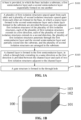
- An embodiment of the application provides a method for forming a semiconductor structure. As shown in FIG. 1A , the method includes the following operations.
- a base in which the base includes a substrate, a first semiconductor layer and a second semiconductor layer sequentially formed on one another.
- the substrate may be a silicon substrate, a silicon germanium substrate, or a Silicon On Insulator, SOI, substrate, and may also be a silicon nitride substrate or other suitable substrates.
- a material of the first semiconductor layer may be silicon (Si), germanium (Ge), or silicon germanium (SiGe), silicon carbide (SiC); and may also be Silicon On Insulator, SOI, or Germanium on Insulator, GOI; or may also be other materials, for example, III-V group compounds such as gallium arsenide.
- CMOS Complementary Metal Oxide Semiconductor
- the cost of a silicon germanium process is comparable to the cost of a silicon process.
- the cost of the silicon germanium process is lower than the cost of a gallium arsenide process.
- the second semiconductor layer may be a silicon layer, and may also include other semiconductor elements such as germanium (Ge); or includes semiconductor compounds such as silicon carbide (SiC), gallium arsenide (GaAs), gallium phosphide (GaP), indium phosphide (InP), indium arsenide (InAs), or indium antimonide (InSb); or includes other semiconductor alloys such as silicon germanium (SiGe), gallium arsenide phosphide (GaAsP), indium aluminum arsenide (AlInAs), gallium aluminum arsenide (AlGaAs), indium gallium arsenide (GaInAs), indium gallium phosphide (GaInP), and/or indium gallium arsenide phosphide (GaInAsP) or a combination thereof.
- germanium germanium
- SiC silicon carbide
- GaAs gallium arsenide
- GaP gallium phos
- the first semiconductor layer and the second semiconductor layer may be formed through epitaxy.
- An epitaxial growth method may adopt Molecular Beam Epitaxy, MBE, a combination of ultralow pressure chemical vapor deposition and ultrahigh vacuum technology (Ultrahigh Vacuum Chemical Vapor Deposition, UHV/CVD), Ultra Violet Chemical Vapor Deposition, UV/CVD, Atmospheric Pressure Chemical Vapor Deposition, APCVD, and Rapid Thermal Chemical Vapor Deposition, RT-CVD, or the like.
- UHV/CVD Ultrahigh Vacuum Chemical Vapor Deposition
- UV/CVD Ultra Violet Chemical Vapor Deposition
- APCVD Atmospheric Pressure Chemical Vapor Deposition
- RT-CVD Rapid Thermal Chemical Vapor Deposition
- This capability is not only important for the generation of the doped planes, but also allows the lattice-mismatched materials to be combined with each other in a coherent manner.
- silicon germanium alloy since the carriers in the quantum well composed of silicon (Si) and silicon germanium have a higher mobility, the mobility of electrons thereof is almost twice that of pure silicon. More importantly, when silicon and germanium are alloyed, the free-standing alloy has a diamond crystal lattice, and the lattice constant of the alloy is almost linearly dependent between silicon and germanium values, with a deviation of about 4.17% at room temperature.
- a growing layer attempts to modify its in-plane lattice constant, in order to form a coherent crystal plane with the substrate layer.
- a plurality of first isolation structures spaced apart from each other and a plurality of second isolation structures spaced apart from each other are formed in the base, in which a source layer formed in the second semiconductor layer and a drain layer formed in the substrate are provided between any two adjacent first isolation structures of the plurality of the first isolation structures, each of the plurality of first isolation structures extends in a first direction, each of the plurality of second isolation structures extends in a second direction, the plurality of first isolation structures penetrate through the first semiconductor layer and the second semiconductor layer and partially extend into the substrate, and the plurality of second isolation structures are arranged in the substrate.
- the two directions that intersect with each other are the first direction and the second direction.
- the first direction is defined as the X-axis direction
- the second direction is defined as the Y-axis direction.
- the drain layer and the source layer have opposite conductive types.
- a channel layer is formed in the first semiconductor layer, in which a through hole extending in a same direction as the first direction is provided between the channel layer and each of two first isolation structures adjacent to the channel layer.
- the channel layer is arranged between the drain layer and the source layer.
- a gate structure is formed in the through hole.
- the first isolation structure is configured to isolate the gate structures from each other.
- the gate structure may include a gate oxide layer and a conductive material on a surface of the gate oxide layer.
- the gate oxide layer may serve as a dielectric layer to realize electric isolation between the gate structure and the base.
- the gate oxide layer may be formed through high temperature oxidation, and the temperature for the high temperature oxidation process may be comprised between 900 °C and 1200 °C.
- a material of the gate oxide layer may be silicon oxide, silicon nitride, silicon oxynitride, Oxide/Nitride/Oxide, ONO, or a high-k material with a higher dielectric constant than that of the silicon oxide layer, so that it can effectively prevent boron from polysilicon from diffusing to solve the problem of boron penetration. Meanwhile, a small amount of nitrogen atoms distributed on the interface between the gate oxide layer and the base can also improve characteristics of the interface, thereby enhancing the reliability of the gate oxide layer, and reducing the leakage current.
- the high-k material may have a dielectric constant comprised between about 10 and 25, and may include, for example, hafnium oxide (HfO 2 ), aluminum oxide (Al 2 O 3 ), hafnium aluminum oxide (HfAlO 3 ), tantalum oxide (Ta 2 O 3 ), and/or titanium oxide (TiO 2 ).
- HfO 2 hafnium oxide
- Al 2 O 3 aluminum oxide
- HfAlO 3 hafnium aluminum oxide
- Ta 2 O 3 tantalum oxide
- TiO 2 titanium oxide
- the plurality of first isolation structures and the plurality of second isolation structures are formed in the base, the channel layer is formed in the first semiconductor layer, and the gate structure is formed in the through hole of the channel layer, so that gate self-alignment is realized, and a gate all round structure is formed, thereby improving the gate control capability and the switching speed.
- S101 to S104 are illustrated respectively with reference to FIG. 1B to FIG. 1E .
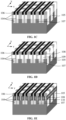
- the base 100 includes a substrate 101, a first semiconductor layer 102, and a second semiconductor layer 103 which are sequentially formed on one another.
- a plurality of first isolation structures 104 spaced apart from each other and a plurality of second isolation structures 105 spaced apart from each other are formed in the base (see the base 100 shown in FIG. 1B ).
- a source layer 106 formed in the second semiconductor layer (see the second semiconductor layer 103 shown in FIG. 1B ) and a drain layer 107 formed in the substrate (see the substrate 101 shown in FIG. 1B ) are provided between any two adjacent first isolation structures 104.
- Each first isolation structure 104 extends in the X-axis direction
- each second isolation structure 105 extends in the Y-axis direction.
- the plurality of first isolation structures 104 penetrate through the first semiconductor layer (see the first semiconductor layer 102 shown in FIG. 1B ) and the second semiconductor layer 103, and partially extend into the substrate 101.
- the plurality of second isolation structures 105 are arranged in the substrate 101.
- a channel layer 108 is formed in the first semiconductor layer (see the first semiconductor layer 102 shown in FIG. 1B ).
- a through hole 109 extending in a same direction as the first direction is provided between the channel layer 108 and each of two first isolation structures 104 adjacent to the channel layer.
- a gate structure 110 is formed in the through hole 109 (see the through hole 109 shown in FIG. 1D ).
- the semiconductor structure includes:
- the substrate is a silicon substrate
- the first semiconductor layer is a silicon germanium layer
- the second semiconductor layer is a silicon layer.
- the carriers in the silicon germanium layer have a higher mobility, and the electron mobility thereof is twice that of the pure silicon layer.
- the gate structure includes a gate oxide layer, and a conductive material on a surface of the gate oxide layer.
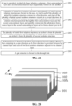
- An embodiment of the application further provides a method for forming a semiconductor structure. As shown in FIG. 2A , the method includes the following operations.
- a base in which the base includes a substrate, a first semiconductor layer and a second semiconductor layer sequentially formed on one another.
- a plurality of initial first isolation structures and a plurality of initial second isolation structures are formed in the base, in which each of the plurality of initial first isolation structures extends in a first direction, and each of the plurality of initial second isolation structures extends in a second direction, and in which the plurality of initial first isolation structures and the plurality of initial second isolation structures penetrate through the first semiconductor layer and the second semiconductor layer, and partially extend into the substrate to form a source layer in the second semiconductor layer and to form a drain layer in the substrate.
- the plurality of initial first isolation structures are etched to form the plurality of first isolation structures, and the plurality of initial second isolation structures are etched to form the plurality of second isolation structures.
- a channel layer is formed in the first semiconductor layer, in which a through hole extending in a same direction as the first direction is provided between the channel layer and each of two first isolation structures adjacent to the channel layer.
- a gate structure is formed in the through hole.
- the operation that the plurality of first isolation structures spaced apart from each other and the plurality of second isolation structures spaced apart from each other are formed in the base in the above embodiment may be implemented through S201 to S203.
- S202 may be implemented through S221 and S222.
- S221 is implemented with reference to FIG. 2B to FIG. 2C
- S222 is implemented with reference to FIG. 2D to FIG. 2E .
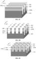
- a plurality of second isolation structure trenches 105a (in the Y-axis direction) is formed in the base (see the base 100 shown in FIG. 1B ).
- the plurality of second isolation structure trenches (see the second isolation structure trench 105a shown in FIG. 2B ) are filled with a first dielectric layer 105b to form the plurality of initial second isolation structures.
- a plurality of first isolation structure trenches 104a (in the X-axis direction) are formed in the base.
- the plurality of first isolation structure trenches are filled with a second dielectric layer 104b and a third dielectric layer 104c to form the plurality of initial first isolation structures 104d.
- the plurality of first isolation structure trenches (see the first isolation structure trench 104a shown in FIG. 2D ) and the plurality of second isolation structure trenches (see the second isolation structure trench 105a shown in FIG. 2B ) penetrate through the first semiconductor layer 102 and the second semiconductor layer 103, and partially extend into the substrate 101.
- the first isolation structure trench and the second isolation structure trench may be formed through a self-aligned shallow trench isolation technology, for example, may be formed through a Self-aligned Double Patterning, SADP, process, or may be formed through a Self-aligned Quadruple Patterning, SAQP, process.
- SADP Self-aligned Double Patterning
- SAQP Self-aligned Quadruple Patterning
- a Sacrifice Layer (generally a CVD material) can be deposited on the surface of the base, and then photolithography and etching are performed to transfer the pattern on the mask to the sacrifice layer.
- the pattern on the sacrifice layer is also called a "mandrel” or “core”.
- ALD Atomic Layer Deposition, ALD is used for depositing a thin film (called a "spacer material") of a relatively uniform thickness on a surface and a side of the "mandrel”. The deposited spacer material is then etched through a reactive ion etching process, and this operation is known as "etch back".
- the material deposited on both sides of the pattern remains to form so-called spacer.
- the "mandrel” is removed by using a high-selectivity etchant, and only the spacer is remained on the surface of the base.
- a cycle of the spacer pattern is half of that of a photolithography pattern, so that doubling of the spatial pattern density is realized.
- the spacer pattern is transferred to a hard mask of the base through plasma etching.
- the material of the first dielectric layer may be silicon oxide, for example, silicon dioxide, silicon oxynitride or silicon oxide doped with boron and phosphorus, or other suitable materials.
- the material of the second dielectric layer may be the same as or different from the material of the first dielectric layer.
- the first dielectric layer may be formed through thermal oxidation, Chemical Vapor Deposition, CVD, Atomic Layer Deposition, ALD, Plasma Enhanced Atomic Layer Deposition, PEALD, Low Pressure Chemical Vapor Deposition, LPCVD, or other suitable processes.
- the second dielectric layer may be formed through the same process as the first dielectric layer, or may be formed through a different process from the first dielectric layer.
- the material of the third dielectric layer may be nitrides, such as silicon nitride, aluminum nitride (AlN), gallium nitride (GaN) and indium nitride (InN), and may be formed through a process such as LPCVD, Atmospheric Pressure Chemical Vapor Deposition, APCVD, or atomic layer deposition.
- nitrides such as silicon nitride, aluminum nitride (AlN), gallium nitride (GaN) and indium nitride (InN)
- the material of the first dielectric layer includes silicon oxide, and the material of the second dielectric layer is the same as the material of the first dielectric layer.
- the operation that the plurality of first isolation structure trenches are filled with the second dielectric layer and the third dielectric layer to form the plurality of initial first isolation structures may be implemented through S2221 to S2223.
- the plurality of first isolation structure trenches are filled with the second dielectric layer.
- the plurality of first isolation structure trenches are filled with the third dielectric layer to form the plurality of initial first isolation structures.
- the second dielectric layer at the bottom portion of each of the plurality of first isolation structure trenches may be removed through a dry etching process or a wet etching process.
- the dry etching process may be a plasma etching process, a reactive ion etching process, or an ion milling process.
- the second dielectric layer on the surface of the second semiconductor layer may be removed through a Chemical Mechanical Polish, CMP, process.
- the operations S222a and S222b are further included between S2222 and S2223, with reference to FIG. 2F .
- the operations are as follows.
- metal cobalt is deposited at the bottom portion of each of the plurality of first isolation structure trenches (see the first isolation structure trench 104a shown in FIG. 2D ).
- annealing treatment is performed to form silicide in the substrate 101 to form a buried bit line 114, in which the drain layer 107 is arranged between the channel layer (see the channel layer 108 shown in FIG. 1E ) and the buried bit line 114, and the plurality of initial second isolation structures penetrate through the buried bit line 114.
- a substance deposited at the bottom portion of the first isolation structure trench is not limited to the metal cobalt, and may also be any one of titanium (Ti), tantalum (Ta), nickel (Ni), tungsten (W), platinum (Pt), and Palladium (Pd).
- the above metal can be deposited through CVD or ALD.
- the annealing treatment allows the metal and the substrate to react with each other to achieve silicidation.
- Rapid annealing may be performed through rapid thermal annealing at different temperatures according the types of the deposited metal and the substrate. For example, if the metal material is cobalt, the annealing temperature may range from 400 °C to 800 °C.
- the metal silicide formed after silicidation may serve as the buried bit line.
- the metal silicide is a substance with a lower resistance than that of polysilicon. With such a substance, the buried bit line has a low resistance.
- the buried bit line may be formed through a silicidation process.
- the buried bit line may be formed through a complete silicidation process.
- the complete silicidation process is a process for completely silicidating a silicon-containing substance to a desired depth.
- the buried bit line may be formed by using a near-noble metal such as titanium silicide (TiSi x ), tungsten silicide (WSi x ), cobalt silicide (CoSi x ), and nickel silicide (NiSi x ), or a metal silicide such as a refractory metal.
- the metal silicide may be obtained by forming a conductive material through a sputtering process, a CVD process or an ALD process, and then performing the silicidation process.
- the conductive material may include the near-noble metal or the refractory metal.
- the buried bit line is subjected to the complete silicidation, so that the resistance of the buried bit line may be reduced.
- S203 may be implemented through S231 to S233, and S231 to S232 are respectively shown in FIG. 2G to FIG. 2I .
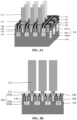
- the second dielectric layer 104b in the plurality of initial first isolation structures 104d in the second semiconductor 103 is etched, and the first dielectric layer 105b in the plurality of initial second isolation structures (see the description regarding to S221) in the second semiconductor layer 103 is etched, so that the structure shown in FIG. 2G can be formed.
- the plurality of etched initial first isolation structures (see the initial first isolation structure 104d shown in FIG. 2E ) in the second semiconductor layer 103 are filled with a fourth dielectric layer 104e, so that the structure shown in FIG. 2H can be formed.
- the second dielectric layer 104b in the plurality of initial first isolation structures (see the initial first isolation structure 104d shown in FIG. 2E ) in the first semiconductor layer 102 is etched, and the first dielectric layer 105b in the plurality of initial second isolation structures (see the description regarding to S221) in the first semiconductor layer 102 is etched, so as to form the plurality of first isolation structures 104 and the plurality of second isolation structures 105, so that the structure shown in FIG. 2I can be formed.
- each first isolation structure 104 includes the second dielectric layer 104b, the third dielectric layer 104c, and the fourth dielectric layer 104e.
- a material of the third dielectric layer includes silicon nitride, and a material of the fourth dielectric layer is the same as the material of the third dielectric layer.
- the method further includes S234, in which, with reference to FIG. 2I , a portion of the first semiconductor layer (see the first semiconductor layer 102 shown in FIG. 2H ) is etched to form the channel layer 108 as shown in FIG. 2J .
- the through hole 109 extending in the same direction as the first direction is provided between the channel layer 108 and each of the two first isolation structures 104 adjacent to the channel layer.
- the first semiconductor layer may be etched along the first direction (i.e., the X-axis direction) through an isotropic quasi-atomic layer etching technology to form the channel layer.
- the dimension of the channel layer may be controlled, so that the control of the channel by the grate structure can be improved, while improving the switching speed.
- S205 is performed.
- the structure shown in FIG. 2K is formed after the gate structure is formed in the through hole.
- the semiconductor structure includes:
- An embodiment of the application further provides a method for forming a semiconductor structure, which includes the following operations.
- a base 100 in which the base includes a substrate 101, a first semiconductor layer 102 and a second semiconductor layer 103 sequentially formed on one another.
- ion doping is performed on the second semiconductor layer 103 and a portion of the substrate 101, so as to form a drain doped area in the substrate 101, and to form a source doped area in the second semiconductor layer 103.
- the dopant used for ion doping may be an N-type dopant, such as phosphorus (P), arsenic (As), silicon (Si), germanium (Ge), carbon (C), oxygen (O), sulfur (S), selenium (Se), tellurium (Te), or antimony (Sb); and may also be a P-type dopant, such as boron (B), boron fluoride (BF 2 ), silicon, germanium, carbon, Zinc (Zn), cadmium (Cd), beryllium (Be), magnesium (Mg), or indium (In).
- N-type dopant such as phosphorus (P), arsenic (As), silicon (Si), germanium (Ge), carbon (C), oxygen (O), sulfur (S), selenium (Se), tellurium (Te), or antimony (Sb); and may also be a P-type dopant, such as boron (B), boron fluoride (BF 2 ), silicon,
- a plurality of first isolation structures 104 spaced apart from each other and a plurality of second isolation structures 105 spaced apart from each other are formed in the base (see the base 100 shown in FIG. 1B ), in which a source layer 106 formed in the second semiconductor layer 103 and a drain layer 107 formed in the substrate 101 are provided between any two adjacent first isolation structures 104 of the plurality of first isolation structures, each of the plurality of first isolation structures 104 extends in a first direction, each of the plurality of second isolation structures 105 extends in a second direction, the plurality of first isolation structures 104 penetrate through the first semiconductor layer 102 and the second semiconductor layer 103 and partially extend into the substrate 101, and the plurality of second isolation structures are arranged in the substrate 101.
- a channel layer 108 is formed in the first semiconductor layer 102, in which a through hole 109 extending in a same direction as the first direction is provided between the channel layer 108 and each of two first isolation structures 104 adjacent to the channel layer.
- a gate structure 110 is formed in the through hole (see the through hole 109 shown in FIG. 1D ).
- the second semiconductor layer 103 is filled with a fifth dielectric layer 111.
- a top surface of the fifth dielectric layer 111 is flush with a top surface of the second semiconductor layer 103.
- a material of the fifth dielectric layer may be nitrides, such as silicon nitride, aluminum nitride (AlN), gallium nitride (GaN), and indium nitride (InN), and the fifth dielectric layer can be formed through a process such as low pressure chemical vapor deposition, atmospheric pressure chemical vapor deposition, or atomic layer deposition.
- a contact node 112 and a capacitor 113 are sequentially formed on each source layer 106.
- the capacitor may be a pillar capacitor, but may not be limited to a cylindrical capacitor.
- the capacitor may also be a square capacitor or a pillar capacitor of other shapes.
- the contact node may have a pillar shape or a concave structure.
- S305 may be implemented through S3051 and S3052.
- a gate oxide layer is formed in the through hole through thermal oxidation.
- a surface of the gate oxide layer is filled with a conductive material to form the gate structure.
- the conductive material may be a metal, such as tungsten (W), or may be a metal nitride, such as titanium nitride.
- the capacitor may include an electrode plate and a dielectric layer.
- a material of the electrode plate may be titanium nitride (TiN) or aluminum foil, and a material of the dielectric layer may be a composite material of zirconia (ZrO) and aluminum oxide, a zirconia material, an aluminum oxide material or other materials with a higher dielectric constant than that of silicon dioxide.
- the first isolation structures and the second isolation structures are formed in the base, the channel layer is formed in the first semiconductor layer, and the gate structure is formed in the through hole of the channel layer, so that a gate all round structure is formed, thereby improving the gate control capability and the switching speed.
- FIG. 3A and FIG. 3B The semiconductor structure formed by the above method is shown in FIG. 3A and FIG. 3B .
- an embodiment of the application provides a semiconductor structure, which includes: a base (see the base 100 shown in FIG. 1B ), in which the base includes a substrate 101, a first semiconductor layer 102 and a second semiconductor layer 103 sequentially formed on one another;
- the structure further includes a buried bit line 114 arranged in the substrate (see the substrate 101 shown in FIG. 3A ) and penetrated by the plurality of second isolation structures 105.
- the drain layer 107 is arranged between the channel layer 108 and the buried bit line 114.
- a height of a portion of each of the plurality of first isolation structures 104 extending into the substrate is less than a height of a portion of each of the plurality of second isolation structures 105 arranged in the substrate.
- An embodiment of the application further provides a method for forming a semiconductor structure.
- the method includes the following operations.
- a base 100 in which the base 100 includes a substrate 101, a first semiconductor layer 102 and a second semiconductor layer 103 sequentially formed on one another.
- a plurality of second isolation structure trenches 105a are formed in the base (see the base 100 shown in FIG. 1B ); and with reference to FIG. 2C , the plurality of second isolation structure trenches (see the second isolation structure trench 105a shown in FIG. 2C ) are filled with a first dielectric layer 105b to form the plurality of initial second isolation structures.
- the plurality of second isolation structure trenches 105a penetrate through the first semiconductor layer 102 and the second semiconductor layer 103, and partially extend into the substrate 101.
- a plurality of first isolation structure trenches 104a are formed in the base, in which the plurality of first isolation structure trenches 104a penetrate through the first semiconductor layer 102 and the second semiconductor layer 103 and partially extend into the substrate 101, and the source layer 106 formed in the second semiconductor layer 103 and the drain layer 107 formed in the substrate 101 are provided between any two adjacent first isolation structure trenches 104a.
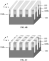
- the plurality of first isolation structure trenches 104a shown in FIG. 2D are filled with the second dielectric layer 104b, so that the structure shown in FIG. 4B can be formed.
- metal cobalt is deposited at the bottom portion of each of the plurality of first isolation structure trenches (see the first isolation structure trench 104a shown in FIG. 4A ); and with reference to FIG. 2F , annealing treatment is performed to form silicide in the substrate to form a buried bit line 114.
- the plurality of first isolation structure trenches are filled with the third dielectric layer 104c to form the plurality of initial first isolation structures 104d.
- the second dielectric layer 104b in the plurality of initial first isolation structures (see the initial first isolation structure 104d shown in FIG. 4D ) in the second semiconductor layer 103 is etched, and the first dielectric layer 105b in the plurality of initial second isolation structures (see the description regarding to S221) in the second semiconductor layer 103 is etched, so that the structure shown in FIG. 2G can be formed.
- the plurality of etched initial first isolation structures (see the initial first isolation structure 104d shown in FIG. 4D ) in the second semiconductor layer 103 are filled with a fourth dielectric layer 104e, so that the structure shown in FIG. 2H can be formed.
- the second dielectric layer 104b in the plurality of initial first isolation structures (see the initial first isolation structure 104d shown in FIG. 4D ) in the first semiconductor layer 102 is etched, and the first dielectric layer 105b in the plurality of initial second isolation structures (see the description regarding to S221) in the first semiconductor layer 102 is etched, so as to form the plurality of first isolation structures 104 and the plurality of second isolation structures 105, so that the structure shown in FIG. 2I can be formed.
- a portion of the first semiconductor layer (see the first semiconductor layer 102 shown in FIG. 2H ) is etched to form the channel layer 108 shown in FIG. 2J , in which a through hole 109 extending in a same direction as the first direction is provided between the channel layer 108 and each of two first isolation structures 104 adjacent to the channel layer, a width of the channel layer 108 in the second direction is less than each of a width of the source layer 106 and a width of the drain layer 107 in the second direction, and the drain layer 107 is arranged between the channel layer 108 and the buried bit line 114.
- a gate oxide layer 110a is formed in the through hole (see the through hole 109 shown in FIG. 2J ) through thermal oxidation.
- a surface of the gate oxide layer 110a is filled with a conductive material 110b to form the gate structure 110.
- the second semiconductor layer 103 is filled with a fifth dielectric layer 111, in which a top surface of the fifth dielectric layer 111 is flush with a top surface of the second semiconductor layer 103.
- a contact node 112 and a capacitor 113 are sequentially formed on each source layer 106.
- the disclosed device and method may be implemented in non-target manners.
- the described device embodiments are merely exemplary.
- the unit division is merely logical function division and may be other division in an actual implementation.
- a plurality of units or components may be combined or integrated into another system, or some features may be ignored or not performed.
- the displayed or discussed components may be coupled or directly coupled to each other.
- the units described above as separate components may or may not be physically separated.
- Components presented as units may or may not be physical units, that is, may be located in one place or may be distributed over multiple network units. Part or all of these units may be selected according to practical requirements to achieve the objectives of the solutions of the embodiment.
- the embodiments of the application provide a semiconductor structure and a method for forming a semiconductor structure.
- the method for forming the semiconductor structure includes the following operations.
- a base is provided, in which the base includes a substrate, a first semiconductor layer and a second semiconductor layer sequentially formed on one another.
- a plurality of first isolation structures spaced apart from each other and a plurality of second isolation structures spaced apart from each other are formed in the base, in which a source layer formed in the second semiconductor layer and a drain layer formed in the substrate are provided between any two adjacent first isolation structures of the plurality of first isolation structures, each of the plurality of first isolation structures extends in a first direction, each of the plurality of second isolation structures extends in a second direction, the plurality of first isolation structures penetrate through the first semiconductor layer and the second semiconductor layer and partially extend into the substrate, and the plurality of second isolation structures are arranged in the substrate.
- a channel layer is formed in the first semiconductor layer, in which a through hole extending in a same direction as the first direction is provided between the channel layer and each of two first isolation structures adjacent to the channel layer.
- a gate structure is formed in the through hole. In the embodiments of the application, gate self-alignment is realized and a gate-all-around structure is formed, thereby improving the gate control capability and the switching speed.
Landscapes
- Engineering & Computer Science (AREA)
- Manufacturing & Machinery (AREA)
- Insulated Gate Type Field-Effect Transistor (AREA)
- Semiconductor Memories (AREA)
Abstract
Description
- This application is based on and claims priority to
Chinese Patent Application No. 202111007272.0, filed on August 30, 2021 - The application relates to the technical field of semiconductors, and relates, but is not limited, to a semiconductor structure and a method for forming a semiconductor structure.
- Since a Gate All Around Field Effect Transistor, GAAFET, has better characteristics for controlling a gate, it can achieve better switching characteristics and more effective suppression of short-channel effects, and thus it is considered to be the best candidate as the replacement of the traditional field effect transistors. However, a process for preparing a GAAFET channel is complicated, and random fluctuation of the process is obvious due to the small dimension. Therefore, it is necessary to pay a special attention to the influence of the process fluctuation on the electrical performances of devices and circuits.
- The application provides a semiconductor structure and a method for forming a semiconductor structure.
- In a first aspect, an embodiment of the application provides a method for forming a semiconductor structure, which includes the following operations.
- A base is provided, in which the base includes a substrate, a first semiconductor layer and a second semiconductor layer sequentially formed on one another.
- A plurality of first isolation structures spaced apart from each other and a plurality of second isolation structures spaced apart from each other are formed in the base, in which a source layer formed in the second semiconductor layer and a drain layer formed in the substrate are provided between any two adjacent first isolation structures of the plurality of first isolation structures, each of the plurality of first isolation structures extends in a first direction, each of the plurality of second isolation structures extends in a second direction, the plurality of first isolation structures penetrate through the first semiconductor layer and the second semiconductor layer and partially extend into the substrate, and the plurality of second isolation structures are arranged in the substrate.
- A channel layer is formed in the first semiconductor layer, in which a through hole extending in a same direction as the first direction is provided between the channel layer and each of two first isolation structures adjacent to the channel layer.
- A gate structure is formed in the through hole.
- In one of the embodiments, before the plurality of first isolation structures spaced apart from each other and the plurality of second isolation structures spaced apart from each other are formed in the base, the method further includes the following operation.
- Ion doping is performed on the second semiconductor layer and a portion of the substrate, so as to form a drain doped area in the substrate, and to form a source doped area in the second semiconductor layer.
- In one of the embodiments, the operation that the plurality of first isolation structures spaced apart from each other and the plurality of second isolation structures spaced apart from each other are formed in the base includes the following operations.
- A plurality of initial first isolation structures and a plurality of initial second isolation structures are formed in the base, in which each of the plurality of initial first isolation structures extends in the first direction, and each of the plurality of initial second isolation structures extends in the second direction, and in which the plurality of initial first isolation structures and the plurality of initial second isolation structures penetrate through the first semiconductor layer and the second semiconductor layer, and partially extend into the substrate, so as to form the source layer in the second semiconductor layer and to form the drain layer in the substrate.
- The plurality of initial first isolation structures are etched to form the plurality of first isolation structures, and the plurality of initial second isolation structures are etched to form the plurality of second isolation structures.
- In one of the embodiments, the operation that the plurality of initial first isolation structures and the plurality of initial second isolation structures are formed in the base includes the following operations.
- A plurality of second isolation structure trenches are formed in the base, and the plurality of second isolation structure trenches are filled with a first dielectric layer, so as to form the plurality of initial second isolation structures.
- After the plurality of initial second isolation structures are formed in the base, a plurality of first isolation structure trenches are formed in the base, and the plurality of first isolation structure trenches are filled with a second dielectric layer and a third dielectric layer to form the plurality of initial first isolation structures, in which the plurality of first isolation structure trenches and the plurality of second isolation structure trenches penetrate through the first semiconductor layer and the second semiconductor layer, and partially extend into the substrate.
- In one of the embodiments, the operation that the plurality of first isolation structure trenches are filled with the second dielectric layer and the third dielectric layer to form the plurality of initial first isolation structures includes the following operations.
- The plurality of first isolation structure trenches are filled with the second dielectric layer.
- The second dielectric layer at a bottom portion of each of the plurality of first isolation structure trenches and on a surface of the second semiconductor layer is removed.
- The plurality of first isolation structure trenches are filled with the third dielectric layer to form the plurality of initial first isolation structures.
- In one of the embodiments, the operation that the plurality of initial first isolation structures are etched to form the plurality of first isolation structures, and the plurality of initial second isolation structures are etched to form the plurality of second isolation structures includes the following operations.
- The second dielectric layer in the plurality of initial first isolation structures in the second semiconductor layer is etched, and the first dielectric layer in the plurality of initial second isolation structures in the second semiconductor layer is etched.
- The plurality of etched initial first isolation structures in the second semiconductor layer are filled with a fourth dielectric layer.
- The second dielectric layer in the plurality of initial first isolation structures in the first semiconductor layer is etched, and the first dielectric layer in the plurality of initial second isolation structures in the first semiconductor layer is etched to form the plurality of first isolation structures and the plurality of second isolation structures.
- In one of the embodiments, after the second dielectric layer in the plurality of initial first isolation structures in the first semiconductor layer is etched and the first dielectric layer in the plurality of initial second isolation structures in the first semiconductor layer is etched, the method includes the following operation.
- A portion of the first semiconductor layer is etched to form the channel layer, in which the through hole extending in the same direction as the first direction is provided between the channel layer and each of the two first isolation structures adjacent to the channel layer, and a width of the channel layer in the second direction is less than each of a width of the source layer and a width of the drain layer in the second direction.
- In one of the embodiments, after the second dielectric layer at the bottom portion of each of the plurality of first isolation structure trenches and on the surface of the second semiconductor layer is removed, and before the plurality of first isolation structure trenches are filled with the third dielectric layer, the method further includes the following operations.
- Metal cobalt is deposited at the bottom portion of each of the plurality of first isolation structure trenches.
- An annealing treatment is performed to form silicide in the substrate, so as to form a buried bit line, in which the drain layer is arranged between the channel layer and the buried bit line, a height of a portion of each of the plurality of first isolation structures extending into the substrate is less than a height of a portion of each of the plurality of second isolation structures arranged in the substrate, and the plurality of second isolation structures penetrate through the buried bit line.
- In one of the embodiments, the operation that the gate structure is formed in the through hole includes the following operations.
- A gate oxide layer is formed in the through hole through thermal oxidation.
- A surface of the gate oxide layer is filled with a conductive material to form the gate structure.
- In one of the embodiments, the method further includes the following operations.
- The second semiconductor layer is filled with a fifth dielectric layer, in which a top surface of the fifth dielectric layer is flush with a top surface of the second semiconductor layer.
- A contact node and a capacitor are sequentially formed on the source layer.
- In one of the embodiments, a material of the first dielectric layer includes silicon oxide, and a material of the second dielectric layer is the same as the material of the first dielectric layer. A material of the third dielectric layer includes a silicon nitride, and a material of the fourth dielectric layer is the same as the material of the third dielectric layer.
- In one of the embodiments, a material of the gate oxide layer includes silicon oxide, and a material of the fifth dielectric layer includes silicon nitride.
- In a second aspect, an embodiment of the application further provides a semiconductor structure. The semiconductor structure includes:
- a base, in which the base includes a substrate, a first semiconductor layer and a second semiconductor layer sequentially formed on one another;
- a plurality of first isolation structures spaced apart from each other and a plurality of second isolation structures spaced apart from each other in the base, in which each the plurality of first isolation structures extends in a first direction, each of the plurality of second isolation structures extends in a second direction, the plurality of first isolation structures penetrate through the first semiconductor layer and the second semiconductor layer and partially extend into the substrate, and the plurality of second isolation structures are arranged in the substrate;
- a source layer arranged in the second semiconductor layer;
- a drain layer arranged in the substrate;
- a channel layer arranged in the first semiconductor layer; and
- a gate structure arranged between the channel layer and each of two first isolation structures adjacent to the channel layer and extending in a same direction as the first direction.
- In one of the embodiments, each of the plurality of first isolation structures includes: a second dielectric layer arranged in the substrate, a fourth dielectric layer arranged in the second semiconductor layer, and a third dielectric layer penetrating through the first semiconductor layer and the second semiconductor layer and partially extending into the substrate. A side wall of the third dielectric layer is in contact with each of the second dielectric layer and the fourth dielectric layer, and each of the plurality of second isolation structures includes a first dielectric layer arranged in the substrate.
- In one of the embodiments, the semiconductor structure further includes a buried bit line arranged in the substrate and penetrated by the plurality of second isolation structures. The drain layer is arranged between the channel layer and the buried bit line, and a height of a portion of each of the plurality of first isolation structures extending into the substrate is less than a height of a portion of each of the plurality of second isolation structures arranged in the substrate.
- In one of the embodiments, the substrate is a silicon substrate, the first semiconductor layer is a silicon germanium layer, and the second semiconductor layer is a silicon layer.
- In one of the embodiments, the gate structure includes a gate oxide layer, and a conductive material on a surface of the gate oxide layer.
- In one of the embodiments, the semiconductor structure further includes:
- a fifth dielectric layer arranged in the second semiconductor layer, in which a top surface of the fifth dielectric layer is flush with a top surface of the second semiconductor layer; and
- a contact node and a capacitor arranged on the source layer.
- In one of the embodiments, a material of the first dielectric layer includes silicon oxide, and a material of the second dielectric layer is the same as the material of the first dielectric layer. A material of the third dielectric layer includes silicon nitride, and a material of the fourth dielectric layer is the same as the material of the third dielectric layer.
- The embodiments of the application provide a semiconductor structure and a method for forming a semiconductor structure. The method for forming the semiconductor structure includes the following operations. A base is provided, in which the base includes a substrate, a first semiconductor layer and a second semiconductor layer sequentially formed on one another. A plurality of first isolation structures spaced apart from each other and a plurality of second isolation structures spaced apart from each other are formed in the base, in which a source layer formed in the second semiconductor layer and a drain layer formed in the substrate are provided between any two adjacent first isolation structures of the plurality of first isolation structures, each of the plurality of first isolation structures extends in a first direction, each of the plurality of second isolation structures extends in a second direction, the plurality of first isolation structures penetrate through the first semiconductor layer and the second semiconductor layer and partially extend into the substrate, and the plurality of second isolation structures are arranged in the substrate. A channel layer is formed in the first semiconductor layer, in which a through hole extending in a same direction as the first direction is provided between the channel layer and each of two first isolation structures adjacent to the channel layer. A gate structure is formed in the through hole. In the embodiments of the application, gate self-alignment is realized and a gate all around structure is formed, thereby improving the gate control capability and the switching speed.
- In the accompanying drawings (which are not necessarily drawn to scale), similar reference numerals may denote similar components in different diagrams. The similar reference numerals having different letter suffixes may denote different examples of the similar components. The accompanying drawings generally illustrate various embodiments discussed in the application by way of example and not by way of limitation.
-
FIG. 1A is a flowchart of a method for forming a semiconductor structure according to an embodiment of the application; -
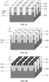
FIG. 1B to FIG. 1E are schematic diagrams of a forming process of a semiconductor structure according to an embodiment of the application; -
FIG. 2A is another flowchart of a method for forming a semiconductor structure according to an embodiment of the application; -
FIG. 2B to FIG. 2K are other schematic diagrams of a forming process of a semiconductor structure according to an embodiment of the application; -
FIG. 3A is a schematic diagram of a semiconductor structure according to an embodiment of the application; -
FIG. 3B is a front view of the structure shown inFIG. 3A ; -
FIG. 4A is another flowchart of a method for forming a semiconductor structure according to an embodiment of the application; and -
FIG. 4B to FIG. 4E are other schematic diagrams of a forming process of a semiconductor structure according to an embodiment of the application. - Exemplary embodiments of the application will be described in more detail below with reference to the accompanying drawings. Although the exemplary embodiments of the application are shown in the accompanying drawings, it should be understood that the application can be implemented in various forms and cannot be limited by specific embodiments illustrated herein. On the contrary, these embodiments are provided to more thoroughly understand the application and to completely convey the scope of the application to those skilled in the art.
- In the following description, numerous specific details are set forth in order to provide a more thorough understanding of the application. However, it will be apparent for those skilled in the art that the application can be implemented without one or more of these details. In other examples, in order to avoid confusion with the application, some technical features known in the art are not described. That is, all the features of the actual embodiments are not described here, and the well-known functions and structures are not described in detail.
- An embodiment of the application provides a method for forming a semiconductor structure. As shown in
FIG. 1A , the method includes the following operations. - In S101, a base is provided, in which the base includes a substrate, a first semiconductor layer and a second semiconductor layer sequentially formed on one another.
- The substrate may be a silicon substrate, a silicon germanium substrate, or a Silicon On Insulator, SOI, substrate, and may also be a silicon nitride substrate or other suitable substrates.
- A material of the first semiconductor layer may be silicon (Si), germanium (Ge), or silicon germanium (SiGe), silicon carbide (SiC); and may also be Silicon On Insulator, SOI, or Germanium on Insulator, GOI; or may also be other materials, for example, III-V group compounds such as gallium arsenide. In terms of a Complementary Metal Oxide Semiconductor, CMOS, process, the cost of a silicon germanium process is comparable to the cost of a silicon process. However, in terms of the heterojunction technology, the cost of the silicon germanium process is lower than the cost of a gallium arsenide process.
- The second semiconductor layer may be a silicon layer, and may also include other semiconductor elements such as germanium (Ge); or includes semiconductor compounds such as silicon carbide (SiC), gallium arsenide (GaAs), gallium phosphide (GaP), indium phosphide (InP), indium arsenide (InAs), or indium antimonide (InSb); or includes other semiconductor alloys such as silicon germanium (SiGe), gallium arsenide phosphide (GaAsP), indium aluminum arsenide (AlInAs), gallium aluminum arsenide (AlGaAs), indium gallium arsenide (GaInAs), indium gallium phosphide (GaInP), and/or indium gallium arsenide phosphide (GaInAsP) or a combination thereof.
- In some embodiments, the first semiconductor layer and the second semiconductor layer may be formed through epitaxy. An epitaxial growth method may adopt Molecular Beam Epitaxy, MBE, a combination of ultralow pressure chemical vapor deposition and ultrahigh vacuum technology (Ultrahigh Vacuum Chemical Vapor Deposition, UHV/CVD), Ultra Violet Chemical Vapor Deposition, UV/CVD, Atmospheric Pressure Chemical Vapor Deposition, APCVD, and Rapid Thermal Chemical Vapor Deposition, RT-CVD, or the like. These technologies have the advantage that they can grow an epitaxial layer at a low temperature (from 300 degrees Celsius, °C, to 700 °C). This capability is not only important for the generation of the doped planes, but also allows the lattice-mismatched materials to be combined with each other in a coherent manner. In the silicon germanium alloy, since the carriers in the quantum well composed of silicon (Si) and silicon germanium have a higher mobility, the mobility of electrons thereof is almost twice that of pure silicon. More importantly, when silicon and germanium are alloyed, the free-standing alloy has a diamond crystal lattice, and the lattice constant of the alloy is almost linearly dependent between silicon and germanium values, with a deviation of about 4.17% at room temperature. When such a silicon germanium layer is epitaxially grown on a substrate (such as a silicon substrate) with the same lattice constant, a growing layer attempts to modify its in-plane lattice constant, in order to form a coherent crystal plane with the substrate layer.
- In S102, a plurality of first isolation structures spaced apart from each other and a plurality of second isolation structures spaced apart from each other are formed in the base, in which a source layer formed in the second semiconductor layer and a drain layer formed in the substrate are provided between any two adjacent first isolation structures of the plurality of the first isolation structures, each of the plurality of first isolation structures extends in a first direction, each of the plurality of second isolation structures extends in a second direction, the plurality of first isolation structures penetrate through the first semiconductor layer and the second semiconductor layer and partially extend into the substrate, and the plurality of second isolation structures are arranged in the substrate.
- Herein, in a direction of a top surface and a bottom surface of the base (i.e., a plane on which the base is located), the two directions that intersect with each other (e.g., the two directions are perpendicular to each other) are the first direction and the second direction. For example, the first direction is defined as the X-axis direction, and the second direction is defined as the Y-axis direction. The drain layer and the source layer have opposite conductive types.
- In S103, a channel layer is formed in the first semiconductor layer, in which a through hole extending in a same direction as the first direction is provided between the channel layer and each of two first isolation structures adjacent to the channel layer.
- Herein, the channel layer is arranged between the drain layer and the source layer.
- In S104, a gate structure is formed in the through hole.
- Herein, the first isolation structure is configured to isolate the gate structures from each other. The gate structure may include a gate oxide layer and a conductive material on a surface of the gate oxide layer. The gate oxide layer may serve as a dielectric layer to realize electric isolation between the gate structure and the base. The gate oxide layer may be formed through high temperature oxidation, and the temperature for the high temperature oxidation process may be comprised between 900 °C and 1200 °C. A material of the gate oxide layer may be silicon oxide, silicon nitride, silicon oxynitride, Oxide/Nitride/Oxide, ONO, or a high-k material with a higher dielectric constant than that of the silicon oxide layer, so that it can effectively prevent boron from polysilicon from diffusing to solve the problem of boron penetration. Meanwhile, a small amount of nitrogen atoms distributed on the interface between the gate oxide layer and the base can also improve characteristics of the interface, thereby enhancing the reliability of the gate oxide layer, and reducing the leakage current. For example, the high-k material may have a dielectric constant comprised between about 10 and 25, and may include, for example, hafnium oxide (HfO2), aluminum oxide (Al2O3), hafnium aluminum oxide (HfAlO3), tantalum oxide (Ta2O3), and/or titanium oxide (TiO2).
- In the embodiment of the application, the plurality of first isolation structures and the plurality of second isolation structures are formed in the base, the channel layer is formed in the first semiconductor layer, and the gate structure is formed in the through hole of the channel layer, so that gate self-alignment is realized, and a gate all round structure is formed, thereby improving the gate control capability and the switching speed.
- S101 to S104 are illustrated respectively with reference to
FIG. 1B to FIG. 1E . - As shown in
FIG. 1B , thebase 100 includes asubstrate 101, afirst semiconductor layer 102, and asecond semiconductor layer 103 which are sequentially formed on one another. - With reference to
FIG. 1B andFIG. 1C , a plurality offirst isolation structures 104 spaced apart from each other and a plurality ofsecond isolation structures 105 spaced apart from each other are formed in the base (see the base 100 shown inFIG. 1B ). Asource layer 106 formed in the second semiconductor layer (see thesecond semiconductor layer 103 shown inFIG. 1B ) and adrain layer 107 formed in the substrate (see thesubstrate 101 shown inFIG. 1B ) are provided between any two adjacentfirst isolation structures 104. Eachfirst isolation structure 104 extends in the X-axis direction, and eachsecond isolation structure 105 extends in the Y-axis direction. The plurality offirst isolation structures 104 penetrate through the first semiconductor layer (see thefirst semiconductor layer 102 shown inFIG. 1B ) and thesecond semiconductor layer 103, and partially extend into thesubstrate 101. The plurality ofsecond isolation structures 105 are arranged in thesubstrate 101. - As shown in
FIG. 1D , achannel layer 108 is formed in the first semiconductor layer (see thefirst semiconductor layer 102 shown inFIG. 1B ). A throughhole 109 extending in a same direction as the first direction is provided between thechannel layer 108 and each of twofirst isolation structures 104 adjacent to the channel layer. - As shown in
FIG. 1E , agate structure 110 is formed in the through hole 109 (see the throughhole 109 shown inFIG. 1D ). - On the basis of a method for forming a semiconductor structure provided in
FIG. 1A , an embodiment of the application provides a semiconductor structure. As shown inFIG. 1E , the semiconductor structure includes: - a base (see the base 100 shown in
FIG. 1B ), in which the base includes a substrate (see thesubstrate 101 shown inFIG. 1B ), a first semiconductor layer (see thefirst semiconductor layer 102 shown inFIG. 1B ), and a second semiconductor layer (see thesecond semiconductor layer 103 shown inFIG. 1B ) which are sequentially formed on one another; - a plurality of
first isolation structures 104 spaced apart from each other and a plurality ofsecond isolation structures 105 spaced apart from each other in thebase 100, in which eachfirst isolation structure 104 extends in a first direction, eachsecond isolation structure 105 extends in a second direction, the plurality offirst isolation structures 104 penetrate through thefirst semiconductor layer 102 and thesecond semiconductor layer 103 and partially extend into thesubstrate 101, and the plurality ofsecond isolation structures 105 are arranged in thesubstrate 101; - a
source layer 106 arranged in thesecond semiconductor layer 103; - a
drain layer 107 arranged in thesubstrate 101; - a
channel layer 108 arranged in thefirst semiconductor layer 102; and - a
gate structure 110 arranged between thechannel layer 108 and each of twofirst isolation structures 104 adjacent to the channel layer and extending in a same direction as the first direction. - In some embodiments, the substrate is a silicon substrate, the first semiconductor layer is a silicon germanium layer, and the second semiconductor layer is a silicon layer. The carriers in the silicon germanium layer have a higher mobility, and the electron mobility thereof is twice that of the pure silicon layer.
- In some embodiments, the gate structure includes a gate oxide layer, and a conductive material on a surface of the gate oxide layer.
- An embodiment of the application further provides a method for forming a semiconductor structure. As shown in
FIG. 2A , the method includes the following operations. - In S201, a base is provided, in which the base includes a substrate, a first semiconductor layer and a second semiconductor layer sequentially formed on one another.
- In S202, a plurality of initial first isolation structures and a plurality of initial second isolation structures are formed in the base, in which each of the plurality of initial first isolation structures extends in a first direction, and each of the plurality of initial second isolation structures extends in a second direction, and in which the plurality of initial first isolation structures and the plurality of initial second isolation structures penetrate through the first semiconductor layer and the second semiconductor layer, and partially extend into the substrate to form a source layer in the second semiconductor layer and to form a drain layer in the substrate.
- In S203, the plurality of initial first isolation structures are etched to form the plurality of first isolation structures, and the plurality of initial second isolation structures are etched to form the plurality of second isolation structures.
- In S204, a channel layer is formed in the first semiconductor layer, in which a through hole extending in a same direction as the first direction is provided between the channel layer and each of two first isolation structures adjacent to the channel layer.
- In S205, a gate structure is formed in the through hole.
- The operation that the plurality of first isolation structures spaced apart from each other and the plurality of second isolation structures spaced apart from each other are formed in the base in the above embodiment may be implemented through S201 to S203.
- In some embodiments, S202 may be implemented through S221 and S222. S221 is implemented with reference to
FIG. 2B to FIG. 2C , and S222 is implemented with reference toFIG. 2D to FIG. 2E . - In S221, with reference to
FIG. 2B , a plurality of secondisolation structure trenches 105a (in the Y-axis direction) is formed in the base (see the base 100 shown inFIG. 1B ). With reference toFIG. 2C , the plurality of second isolation structure trenches (see the secondisolation structure trench 105a shown inFIG. 2B ) are filled with a firstdielectric layer 105b to form the plurality of initial second isolation structures. - In S222, with reference to
FIG. 2D , after the plurality of initialsecond isolation structures 105c are formed in the base (as shown inFIG. 2C ), a plurality of firstisolation structure trenches 104a (in the X-axis direction) are formed in the base. With reference toFIG. 2E , the plurality of first isolation structure trenches (see the firstisolation structure trench 104a shown inFIG. 2D ) are filled with asecond dielectric layer 104b and a thirddielectric layer 104c to form the plurality of initialfirst isolation structures 104d. The plurality of first isolation structure trenches (see the firstisolation structure trench 104a shown inFIG. 2D ) and the plurality of second isolation structure trenches (see the secondisolation structure trench 105a shown inFIG. 2B ) penetrate through thefirst semiconductor layer 102 and thesecond semiconductor layer 103, and partially extend into thesubstrate 101. - Herein, the first isolation structure trench and the second isolation structure trench may be formed through a self-aligned shallow trench isolation technology, for example, may be formed through a Self-aligned Double Patterning, SADP, process, or may be formed through a Self-aligned Quadruple Patterning, SAQP, process.
- During implementation, firstly, a Sacrifice Layer (generally a CVD material) can be deposited on the surface of the base, and then photolithography and etching are performed to transfer the pattern on the mask to the sacrifice layer. The pattern on the sacrifice layer is also called a "mandrel" or "core". Atomic Layer Deposition, ALD is used for depositing a thin film (called a "spacer material") of a relatively uniform thickness on a surface and a side of the "mandrel". The deposited spacer material is then etched through a reactive ion etching process, and this operation is known as "etch back". Due to the geometric effect of a sidewall of the "mandrel", the material deposited on both sides of the pattern remains to form so-called spacer. The "mandrel" is removed by using a high-selectivity etchant, and only the spacer is remained on the surface of the base. A cycle of the spacer pattern is half of that of a photolithography pattern, so that doubling of the spatial pattern density is realized. Finally, the spacer pattern is transferred to a hard mask of the base through plasma etching.
- Herein, the material of the first dielectric layer may be silicon oxide, for example, silicon dioxide, silicon oxynitride or silicon oxide doped with boron and phosphorus, or other suitable materials. The material of the second dielectric layer may be the same as or different from the material of the first dielectric layer. The first dielectric layer may be formed through thermal oxidation, Chemical Vapor Deposition, CVD, Atomic Layer Deposition, ALD, Plasma Enhanced Atomic Layer Deposition, PEALD, Low Pressure Chemical Vapor Deposition, LPCVD, or other suitable processes. The second dielectric layer may be formed through the same process as the first dielectric layer, or may be formed through a different process from the first dielectric layer.
- The material of the third dielectric layer may be nitrides, such as silicon nitride, aluminum nitride (AlN), gallium nitride (GaN) and indium nitride (InN), and may be formed through a process such as LPCVD, Atmospheric Pressure Chemical Vapor Deposition, APCVD, or atomic layer deposition.
- In some embodiments, the material of the first dielectric layer includes silicon oxide, and the material of the second dielectric layer is the same as the material of the first dielectric layer.
- In some embodiments, in S222, the operation that the plurality of first isolation structure trenches are filled with the second dielectric layer and the third dielectric layer to form the plurality of initial first isolation structures may be implemented through S2221 to S2223.
- In S2221, the plurality of first isolation structure trenches are filled with the second dielectric layer.
- In S2222, the second dielectric layer at a bottom portion of each of the plurality of first isolation structure trenches and on a surface of the second semiconductor layer is removed.
- In S2223, the plurality of first isolation structure trenches are filled with the third dielectric layer to form the plurality of initial first isolation structures.
- In a practical application, the second dielectric layer at the bottom portion of each of the plurality of first isolation structure trenches may be removed through a dry etching process or a wet etching process. The dry etching process may be a plasma etching process, a reactive ion etching process, or an ion milling process. The second dielectric layer on the surface of the second semiconductor layer may be removed through a Chemical Mechanical Polish, CMP, process.
- In some embodiments, the operations S222a and S222b are further included between S2222 and S2223, with reference to
FIG. 2F . The operations are as follows. - In S222a, metal cobalt is deposited at the bottom portion of each of the plurality of first isolation structure trenches (see the first
isolation structure trench 104a shown inFIG. 2D ). - In S222b, annealing treatment is performed to form silicide in the
substrate 101 to form a buriedbit line 114, in which thedrain layer 107 is arranged between the channel layer (see thechannel layer 108 shown inFIG. 1E ) and the buriedbit line 114, and the plurality of initial second isolation structures penetrate through the buriedbit line 114. - In a practical application, a substance deposited at the bottom portion of the first isolation structure trench is not limited to the metal cobalt, and may also be any one of titanium (Ti), tantalum (Ta), nickel (Ni), tungsten (W), platinum (Pt), and Palladium (Pd). The above metal can be deposited through CVD or ALD.
- In a practical application, the annealing treatment allows the metal and the substrate to react with each other to achieve silicidation. Rapid annealing may be performed through rapid thermal annealing at different temperatures according the types of the deposited metal and the substrate. For example, if the metal material is cobalt, the annealing temperature may range from 400 °C to 800 °C. The metal silicide formed after silicidation may serve as the buried bit line.
- The metal silicide is a substance with a lower resistance than that of polysilicon. With such a substance, the buried bit line has a low resistance. The buried bit line may be formed through a silicidation process. In addition, the buried bit line may be formed through a complete silicidation process. The complete silicidation process is a process for completely silicidating a silicon-containing substance to a desired depth. The buried bit line may be formed by using a near-noble metal such as titanium silicide (TiSix), tungsten silicide (WSix), cobalt silicide (CoSix), and nickel silicide (NiSix), or a metal silicide such as a refractory metal. The metal silicide may be obtained by forming a conductive material through a sputtering process, a CVD process or an ALD process, and then performing the silicidation process. The conductive material may include the near-noble metal or the refractory metal. The buried bit line is subjected to the complete silicidation, so that the resistance of the buried bit line may be reduced.
- In some embodiments, S203 may be implemented through S231 to S233, and S231 to S232 are respectively shown in
FIG. 2G to FIG. 2I . - In S231, with reference to
FIG. 2E , thesecond dielectric layer 104b in the plurality of initialfirst isolation structures 104d in thesecond semiconductor 103 is etched, and thefirst dielectric layer 105b in the plurality of initial second isolation structures (see the description regarding to S221) in thesecond semiconductor layer 103 is etched, so that the structure shown inFIG. 2G can be formed. - In S232, with reference to
FIG. 2G , the plurality of etched initial first isolation structures (see the initialfirst isolation structure 104d shown inFIG. 2E ) in thesecond semiconductor layer 103 are filled with afourth dielectric layer 104e, so that the structure shown inFIG. 2H can be formed. - In S233, with reference to
FIG. 2H , thesecond dielectric layer 104b in the plurality of initial first isolation structures (see the initialfirst isolation structure 104d shown inFIG. 2E ) in thefirst semiconductor layer 102 is etched, and thefirst dielectric layer 105b in the plurality of initial second isolation structures (see the description regarding to S221) in thefirst semiconductor layer 102 is etched, so as to form the plurality offirst isolation structures 104 and the plurality ofsecond isolation structures 105, so that the structure shown inFIG. 2I can be formed. - Herein, each
first isolation structure 104 includes thesecond dielectric layer 104b, the thirddielectric layer 104c, and thefourth dielectric layer 104e. - In some embodiments, a material of the third dielectric layer includes silicon nitride, and a material of the fourth dielectric layer is the same as the material of the third dielectric layer.
- In some embodiments, after S233, the method further includes S234, in which, with reference to
FIG. 2I , a portion of the first semiconductor layer (see thefirst semiconductor layer 102 shown inFIG. 2H ) is etched to form thechannel layer 108 as shown inFIG. 2J . The throughhole 109 extending in the same direction as the first direction is provided between thechannel layer 108 and each of the twofirst isolation structures 104 adjacent to the channel layer. - During implementation, the first semiconductor layer may be etched along the first direction (i.e., the X-axis direction) through an isotropic quasi-atomic layer etching technology to form the channel layer. The dimension of the channel layer may be controlled, so that the control of the channel by the grate structure can be improved, while improving the switching speed.
- S205 is performed. The structure shown in
FIG. 2K is formed after the gate structure is formed in the through hole. - On the basis of the structure in
FIG. 2K formed by the above method, an embodiment of the application provides a semiconductor structure. The semiconductor structure includes: - a base (see the base 100 shown in
FIG. 1B ), in which the base includes a substrate (see thesubstrate 101 shown inFIG. 1B ), a first semiconductor layer (see thefirst semiconductor layer 102 shown inFIG. 1B ), and a second semiconductor layer (see thesecond semiconductor layer 103 shown inFIG. 1B ) which are sequentially formed on one another; - a plurality of
first isolation structures 104 spaced apart from each other and a plurality ofsecond isolation structures 105 spaced apart from each other in the base, in which each of the plurality offirst isolation structures 104 extends in a first direction, each of the plurality ofsecond isolation structures 105 extends in a second direction, the plurality offirst isolation structures 104 penetrate through the first semiconductor layer and the second semiconductor layer and partially extend into the substrate, and the plurality ofsecond isolation structures 105 are arranged in the substrate; eachfirst isolation structure 104 includes: asecond dielectric layer 104b arranged in the substrate, afourth dielectric layer 104e arranged in the second semiconductor layer, and a thirddielectric layer 104c penetrating through the first semiconductor layer and the second semiconductor layer and partially extending into the substrate; a side wall of the thirddielectric layer 104c is in contact with each of thesecond dielectric layer 104b and thefourth dielectric layer 104e, and each of the plurality ofsecond isolation structures 105 includes a firstdielectric layer 105b arranged in the substrate; - a
source layer 106 arranged in the second semiconductor layer; - a
drain layer 107 arranged in the substrate; - a
channel layer 108 arranged in the first semiconductor layer; and - a
gate structure 110 arranged between thechannel layer 108 and each of twofirst isolation structures 104 adjacent to the channel layer and extending in a same direction as the first direction. - a buried
bit line 114 arranged in the substrate and penetrated by the plurality ofsecond isolation structures 105, in which thedrain layer 107 is arranged between thechannel layer 108 and the buriedbit line 114, and a height of a portion of each of the plurality offirst isolation structures 104 extending into the substrate is less than a height of a portion of each of the plurality ofsecond isolation structures 105 arranged in the substrate. - An embodiment of the application further provides a method for forming a semiconductor structure, which includes the following operations.
- In S301, as shown in
FIG. 1B , abase 100 is provided, in which the base includes asubstrate 101, afirst semiconductor layer 102 and asecond semiconductor layer 103 sequentially formed on one another. - In S302, ion doping is performed on the
second semiconductor layer 103 and a portion of thesubstrate 101, so as to form a drain doped area in thesubstrate 101, and to form a source doped area in thesecond semiconductor layer 103. - Herein, the dopant used for ion doping may be an N-type dopant, such as phosphorus (P), arsenic (As), silicon (Si), germanium (Ge), carbon (C), oxygen (O), sulfur (S), selenium (Se), tellurium (Te), or antimony (Sb); and may also be a P-type dopant, such as boron (B), boron fluoride (BF2), silicon, germanium, carbon, Zinc (Zn), cadmium (Cd), beryllium (Be), magnesium (Mg), or indium (In).
- In S303, as shown in
FIG. 1C , a plurality offirst isolation structures 104 spaced apart from each other and a plurality ofsecond isolation structures 105 spaced apart from each other are formed in the base (see the base 100 shown inFIG. 1B ), in which asource layer 106 formed in thesecond semiconductor layer 103 and adrain layer 107 formed in thesubstrate 101 are provided between any two adjacentfirst isolation structures 104 of the plurality of first isolation structures, each of the plurality offirst isolation structures 104 extends in a first direction, each of the plurality ofsecond isolation structures 105 extends in a second direction, the plurality offirst isolation structures 104 penetrate through thefirst semiconductor layer 102 and thesecond semiconductor layer 103 and partially extend into thesubstrate 101, and the plurality of second isolation structures are arranged in thesubstrate 101. - In S304, as shown in
FIG. 1D , achannel layer 108 is formed in thefirst semiconductor layer 102, in which a throughhole 109 extending in a same direction as the first direction is provided between thechannel layer 108 and each of twofirst isolation structures 104 adjacent to the channel layer. - In S305, as shown in
FIG. 1E , agate structure 110 is formed in the through hole (see the throughhole 109 shown inFIG. 1D ). - In S306, as shown in
FIG. 3A , thesecond semiconductor layer 103 is filled with a fifthdielectric layer 111. A top surface of thefifth dielectric layer 111 is flush with a top surface of thesecond semiconductor layer 103. - Herein, a material of the fifth dielectric layer may be nitrides, such as silicon nitride, aluminum nitride (AlN), gallium nitride (GaN), and indium nitride (InN), and the fifth dielectric layer can be formed through a process such as low pressure chemical vapor deposition, atmospheric pressure chemical vapor deposition, or atomic layer deposition.
- In S307, as shown in
FIG. 3A , acontact node 112 and acapacitor 113 are sequentially formed on eachsource layer 106. - Herein, the capacitor may be a pillar capacitor, but may not be limited to a cylindrical capacitor. The capacitor may also be a square capacitor or a pillar capacitor of other shapes. The contact node may have a pillar shape or a concave structure.
- In some embodiments, S305 may be implemented through S3051 and S3052.
- In S3051, a gate oxide layer is formed in the through hole through thermal oxidation.
- In S3052, a surface of the gate oxide layer is filled with a conductive material to form the gate structure.
- In a practical application, the conductive material may be a metal, such as tungsten (W), or may be a metal nitride, such as titanium nitride.
- In some embodiments, the capacitor may include an electrode plate and a dielectric layer. A material of the electrode plate may be titanium nitride (TiN) or aluminum foil, and a material of the dielectric layer may be a composite material of zirconia (ZrO) and aluminum oxide, a zirconia material, an aluminum oxide material or other materials with a higher dielectric constant than that of silicon dioxide.
- In the embodiment of the application, the first isolation structures and the second isolation structures are formed in the base, the channel layer is formed in the first semiconductor layer, and the gate structure is formed in the through hole of the channel layer, so that a gate all round structure is formed, thereby improving the gate control capability and the switching speed.
- The semiconductor structure formed by the above method is shown in
FIG. 3A and FIG. 3B . Based onFIG. 3A , an embodiment of the application provides a semiconductor structure, which includes: a base (see the base 100 shown inFIG. 1B ), in which the base includes asubstrate 101, afirst semiconductor layer 102 and asecond semiconductor layer 103 sequentially formed on one another; - a plurality of
first isolation structures 104 spaced apart from each other and a plurality ofsecond isolation structures 105 spaced apart from each other in the base, in which each of the plurality offirst isolation structures 104 extends in a first direction, each of the plurality ofsecond isolation structures 105 extends in a second direction, the plurality offirst isolation structures 104 penetrate through thefirst semiconductor layer 102 and thesecond semiconductor layer 103 and partially extend into thesubstrate 101, and the plurality ofsecond isolation structures 105 are arranged in the substrate; - a
source layer 106 arranged in thesecond semiconductor layer 103; - a
drain layer 107 arranged in thesubstrate 101; - a
channel layer 108 arranged in thefirst semiconductor layer 102; - a
gate structure 110 arranged between thechannel layer 108 and each of twofirst isolation structures 104 adjacent to the channel layer and extending in a same direction as the first direction. - a fifth
dielectric layer 111 arranged in thesecond semiconductor layer 103, in which a top surface of thefifth dielectric layer 111 is flush with a top surface of thesecond semiconductor layer 103; - a
contact node 112 and acapacitor 113 arranged on eachsource layer 106. - In some embodiments, as shown in
FIG. 3A , the structure further includes a buriedbit line 114 arranged in the substrate (see thesubstrate 101 shown inFIG. 3A ) and penetrated by the plurality ofsecond isolation structures 105. Thedrain layer 107 is arranged between thechannel layer 108 and the buriedbit line 114. A height of a portion of each of the plurality offirst isolation structures 104 extending into the substrate is less than a height of a portion of each of the plurality ofsecond isolation structures 105 arranged in the substrate. - An embodiment of the application further provides a method for forming a semiconductor structure. With reference to
FIG. 4A , the method includes the following operations. - In S401, as shown in
FIG. 1B , abase 100 is provided, in which thebase 100 includes asubstrate 101, afirst semiconductor layer 102 and asecond semiconductor layer 103 sequentially formed on one another. - In S402, with reference to
FIG. 2B , a plurality of secondisolation structure trenches 105a are formed in the base (see the base 100 shown inFIG. 1B ); and with reference toFIG. 2C , the plurality of second isolation structure trenches (see the secondisolation structure trench 105a shown inFIG. 2C ) are filled with a firstdielectric layer 105b to form the plurality of initial second isolation structures. - The plurality of second
isolation structure trenches 105a penetrate through thefirst semiconductor layer 102 and thesecond semiconductor layer 103, and partially extend into thesubstrate 101. - In S403, with reference to
FIG. 2D , after the plurality of initial second isolation structures are formed in the base, a plurality of firstisolation structure trenches 104a are formed in the base, in which the plurality of firstisolation structure trenches 104a penetrate through thefirst semiconductor layer 102 and thesecond semiconductor layer 103 and partially extend into thesubstrate 101, and thesource layer 106 formed in thesecond semiconductor layer 103 and thedrain layer 107 formed in thesubstrate 101 are provided between any two adjacent firstisolation structure trenches 104a. - In S404, with reference to
FIG. 2D andFIG. 4B , the plurality of firstisolation structure trenches 104a shown inFIG. 2D are filled with thesecond dielectric layer 104b, so that the structure shown inFIG. 4B can be formed. - In S405, with reference to
FIG. 4B , thesecond dielectric layer 104b at a bottom portion of each of the plurality of first isolation structure trenches (see the firstisolation structure trench 104a shown inFIG. 2D ) and on a surface of thesecond semiconductor layer 103 is removed, so that the structure shown inFIG. 4C can be formed. - In S406, metal cobalt is deposited at the bottom portion of each of the plurality of first isolation structure trenches (see the first
isolation structure trench 104a shown inFIG. 4A ); and with reference toFIG. 2F , annealing treatment is performed to form silicide in the substrate to form a buriedbit line 114. - In S407, with reference to
FIG. 4D , the plurality of first isolation structure trenches (see the firstisolation structure trench 104a shown inFIG. 2D ) are filled with the thirddielectric layer 104c to form the plurality of initialfirst isolation structures 104d. - In S408, with reference to
FIG. 2E , thesecond dielectric layer 104b in the plurality of initial first isolation structures (see the initialfirst isolation structure 104d shown inFIG. 4D ) in thesecond semiconductor layer 103 is etched, and thefirst dielectric layer 105b in the plurality of initial second isolation structures (see the description regarding to S221) in thesecond semiconductor layer 103 is etched, so that the structure shown inFIG. 2G can be formed. - In S409, with reference to
FIG. 2G , the plurality of etched initial first isolation structures (see the initialfirst isolation structure 104d shown inFIG. 4D ) in thesecond semiconductor layer 103 are filled with afourth dielectric layer 104e, so that the structure shown inFIG. 2H can be formed. - In S410, with reference to
FIG. 2H , thesecond dielectric layer 104b in the plurality of initial first isolation structures (see the initialfirst isolation structure 104d shown inFIG. 4D ) in thefirst semiconductor layer 102 is etched, and thefirst dielectric layer 105b in the plurality of initial second isolation structures (see the description regarding to S221) in thefirst semiconductor layer 102 is etched, so as to form the plurality offirst isolation structures 104 and the plurality ofsecond isolation structures 105, so that the structure shown inFIG. 2I can be formed. - In S411, with reference to
FIG. 2I , a portion of the first semiconductor layer (see thefirst semiconductor layer 102 shown inFIG. 2H ) is etched to form thechannel layer 108 shown inFIG. 2J , in which a throughhole 109 extending in a same direction as the first direction is provided between thechannel layer 108 and each of twofirst isolation structures 104 adjacent to the channel layer, a width of thechannel layer 108 in the second direction is less than each of a width of thesource layer 106 and a width of thedrain layer 107 in the second direction, and thedrain layer 107 is arranged between thechannel layer 108 and the buriedbit line 114. - In S412, with reference to
FIG. 2K , agate oxide layer 110a is formed in the through hole (see the throughhole 109 shown inFIG. 2J ) through thermal oxidation. - In S413, with reference to
FIG. 2K , a surface of thegate oxide layer 110a is filled with aconductive material 110b to form thegate structure 110. - In S414, with reference to
FIG. 4E , thesecond semiconductor layer 103 is filled with a fifthdielectric layer 111, in which a top surface of thefifth dielectric layer 111 is flush with a top surface of thesecond semiconductor layer 103. - In S415, with reference to
FIG. 4E , acontact node 112 and acapacitor 113 are sequentially formed on eachsource layer 106. - The above description of the semiconductor structure embodiment is similar to the description of the above method embodiment, and has beneficial effects similar to that of the method embodiment. The understanding for technical details not disclosed in the semiconductor structure embodiments of the application refer to the description of the method embodiments of the application.
- In the several embodiments provided in the application, it should be understood that the disclosed device and method may be implemented in non-target manners. The described device embodiments are merely exemplary. For example, the unit division is merely logical function division and may be other division in an actual implementation. For example, a plurality of units or components may be combined or integrated into another system, or some features may be ignored or not performed. In addition, the displayed or discussed components may be coupled or directly coupled to each other.
- The units described above as separate components may or may not be physically separated. Components presented as units may or may not be physical units, that is, may be located in one place or may be distributed over multiple network units. Part or all of these units may be selected according to practical requirements to achieve the objectives of the solutions of the embodiment.
- The features disclosed in the several method or structure embodiments provided in the application may be combined with each other arbitrarily without conflict, so as to obtain new method embodiments or structure embodiments.
- The above are only some embodiments of the embodiments of the application, but the protection scope of the embodiments of the application is not limited thereto. Any skilled in the art, within the technical scope disclosed by the embodiments of the application, may easily think of variations or replacements, which should be covered within the protection scope of the embodiments of the application. Therefore, the protection scope of the embodiments of the application should be subject to the protection scope of the claims.
- The embodiments of the application provide a semiconductor structure and a method for forming a semiconductor structure. The method for forming the semiconductor structure includes the following operations. A base is provided, in which the base includes a substrate, a first semiconductor layer and a second semiconductor layer sequentially formed on one another. A plurality of first isolation structures spaced apart from each other and a plurality of second isolation structures spaced apart from each other are formed in the base, in which a source layer formed in the second semiconductor layer and a drain layer formed in the substrate are provided between any two adjacent first isolation structures of the plurality of first isolation structures, each of the plurality of first isolation structures extends in a first direction, each of the plurality of second isolation structures extends in a second direction, the plurality of first isolation structures penetrate through the first semiconductor layer and the second semiconductor layer and partially extend into the substrate, and the plurality of second isolation structures are arranged in the substrate. A channel layer is formed in the first semiconductor layer, in which a through hole extending in a same direction as the first direction is provided between the channel layer and each of two first isolation structures adjacent to the channel layer. A gate structure is formed in the through hole. In the embodiments of the application, gate self-alignment is realized and a gate-all-around structure is formed, thereby improving the gate control capability and the switching speed.
Claims (19)
- A method for forming a semiconductor structure, comprising:providing a base, wherein the base comprises a substrate, a first semiconductor layer and a second semiconductor layer sequentially formed on one another;forming a plurality of first isolation structures spaced apart from each other and a plurality of second isolation structures spaced apart from each other in the base, wherein a source layer formed in the second semiconductor layer and a drain layer formed in the substrate are provided between any two adjacent first isolation structures of the plurality of first isolation structures, each of the plurality of first isolation structures extends in a first direction, each of the plurality of second isolation structures extends in a second direction, the plurality of first isolation structures penetrate through the first semiconductor layer and the second semiconductor layer and partially extend into the substrate, and the plurality of second isolation structures are arranged in the substrate;forming a channel layer in the first semiconductor layer, wherein a through hole extending in a same direction as the first direction is provided between the channel layer and each of two first isolation structures adjacent to the channel layer; andforming a gate structure in the through hole.
- The method according to claim 1, wherein the method, before forming the plurality of first isolation structures spaced apart from each other and the plurality of second isolation structures spaced apart from each other in the base, further comprises:
performing ion doping on the second semiconductor layer and a portion of the substrate to form a drain doped area in the substrate, and to form a source doped area in the second semiconductor layer. - The method according to claim 1, wherein forming the plurality of first isolation structures spaced apart from each other and the plurality of second isolation structures spaced apart from each other in the base comprises:forming a plurality of initial first isolation structures and a plurality of initial second isolation structures in the base, wherein each of the plurality of initial first isolation structures extends in the first direction, and each of the plurality of initial second isolation structures extends in the second direction, and wherein the plurality of initial first isolation structures and the plurality of initial second isolation structures penetrate through the first semiconductor layer and the second semiconductor layer, and partially extend into the substrate to form the source layer in the second semiconductor layer and to form the drain layer in the substrate; andetching the plurality of initial first isolation structures to form the plurality of first isolation structures, and etching the plurality of initial second isolation structures to form the plurality of second isolation structures.
- The method according to claim 3, wherein forming the plurality of initial first isolation structures and the plurality of initial second isolation structures in the base comprises:forming a plurality of second isolation structure trenches in the base, and filling the plurality of second isolation structure trenches with a first dielectric layer to form the plurality of initial second isolation structures; andafter forming the plurality of initial second isolation structures in the base, forming a plurality of first isolation structure trenches in the base, and filling the plurality of first isolation structure trenches with a second dielectric layer and a third dielectric layer to form the plurality of initial first isolation structures, wherein the plurality of first isolation structure trenches and the plurality of second isolation structure trenches penetrate through the first semiconductor layer and the second semiconductor layer, and partially extend into the substrate.
- The method according to claim 4, wherein filling the plurality of first isolation structure trenches with the second dielectric layer and the third dielectric layer to form the plurality of initial first isolation structures comprises:filling the plurality of first isolation structure trenches with the second dielectric layer;removing the second dielectric layer at a bottom portion of each of the plurality of first isolation structure trenches and on a surface of the second semiconductor layer; andfiling the plurality of first isolation structure trenches with the third dielectric layer to form the plurality of initial first isolation structures.
- The method according to claim 4, wherein etching the plurality of initial first isolation structures to form the plurality of first isolation structures and etching the plurality of initial second isolation structures to form the plurality of second isolation structures comprises:etching the second dielectric layer in the plurality of initial first isolation structures in the second semiconductor layer, and etching the first dielectric layer in the plurality of initial second isolation structures in the second semiconductor layer;filling the plurality of etched initial first isolation structures in the second semiconductor layer with a fourth dielectric layer; andetching the second dielectric layer in the plurality of initial first isolation structures in the first semiconductor layer, and etching the first dielectric layer in the plurality of initial second isolation structures in the first semiconductor layer to form the plurality of first isolation structures and the plurality of second isolation structures.
- The method according to claim 1, wherein the method, after etching the second dielectric layer in the plurality of initial first isolation structures in the first semiconductor layer and etching the first dielectric layer in the plurality of initial second isolation structures in the first semiconductor layer, comprises:
etching a portion of the first semiconductor layer to form the channel layer, wherein the through hole extending in the same direction as the first direction is provided between the channel layer and each of the two first isolation structures adjacent to the channel layer, and a width of the channel layer in the second direction is less than each of a width of the source layer and a width of the drain layer in the second direction. - The method according to claim 5, wherein the method, after removing the second dielectric layer at the bottom portion of each of the plurality of first isolation structure trenches and on the surface of the second semiconductor layer, and before filing the plurality of first isolation structure trenches with the third dielectric layer, further comprises:depositing metal cobalt at the bottom portion of each of the plurality of first isolation structure trenches; andperforming an annealing treatment to form silicide in the substrate to form a buried bit line, wherein the drain layer is arranged between the channel layer and the buried bit line, a height of a portion of each of the plurality of first isolation structures extending into the substrate is less than a height of a portion of each of the plurality of second isolation structures arranged in the substrate, and the plurality of second isolation structures penetrate through the buried bit line.
- The method according to any one of claims 1 to 8, wherein forming the gate structure in the through hole comprises:forming a gate oxide layer in the through hole through thermal oxidation; andfilling a surface of the gate oxide layer with a conductive material to form the gate structure.
- The method according to claim 9, further comprising:filling the second semiconductor layer with a fifth dielectric layer, wherein a top surface of the fifth dielectric layer is flush with a top surface of the second semiconductor layer; andsequentially forming a contact node and a capacitor on the source layer.
- The method according to claim 5 or 7, wherein a material of the first dielectric layer comprises silicon oxide, and a material of the second dielectric layer is the same as the material of the first dielectric layer, and wherein a material of the third dielectric layer comprises silicon nitride, and a material of the fourth dielectric layer is the same as the material of the third dielectric layer.
- The method according to claim 10, wherein a material of the gate oxide layer comprises silicon oxide, and a material of the fifth dielectric layer comprises silicon nitride.
- A semiconductor structure, comprising:a base, wherein the base comprises a substrate, a first semiconductor layer and a second semiconductor layer sequentially formed on one another;a plurality of first isolation structures spaced apart from each other and a plurality of second isolation structures spaced apart from each other in the base, wherein each of the plurality of first isolation structures extends in a first direction, each of the plurality of second isolation structures extends in a second direction, the plurality of first isolation structures penetrate through the first semiconductor layer and the second semiconductor layer and partially extend into the substrate, and the plurality of second isolation structures are arranged in the substrate;a source layer arranged in the second semiconductor layer;a drain layer arranged in the substrate;a channel layer arranged in the first semiconductor layer; anda gate structure arranged between the channel layer and each of two first isolation structures adjacent to the channel layer and extending in a same direction as the first direction.
- The structure according to claim 13, wherein each of the plurality of first isolation structures comprises: a second dielectric layer arranged in the substrate, a fourth dielectric layer arranged in the second semiconductor layer, and a third dielectric layer penetrating through the first semiconductor layer and the second semiconductor layer and partially extending into the substrate, and wherein a side wall of the third dielectric layer is in contact with each of the second dielectric layer and the fourth dielectric layer, and each of the plurality of second isolation structures comprises a first dielectric layer arranged in the substrate.
- The structure according to claim 14, further comprising: a buried bit line arranged in the substrate and penetrated by the plurality of second isolation structures, wherein the drain layer is arranged between the channel layer and the buried bit line, and a height of a portion of each of the plurality of first isolation structures extending into the substrate is less than a height of a portion of each of the plurality of second isolation structures arranged in the substrate.
- The structure according to claim 13, wherein the substrate is a silicon substrate, the first semiconductor layer is a silicon germanium layer, and the second semiconductor layer is a silicon layer.
- The structure according to claim 16, wherein the gate structure comprises a gate oxide layer, and a conductive material on a surface of the gate oxide layer.
- The structure according to any one of claims 13 to 17, further comprising:a fifth dielectric layer arranged in the second semiconductor layer, wherein a top surface of the fifth dielectric layer is flush with a top surface of the second semiconductor layer; anda contact node and a capacitor arranged on the source layer.
- The structure according to claim 14, wherein a material of the first dielectric layer comprises silicon oxide, and a material of the second dielectric layer is the same as the material of the first dielectric layer, and wherein a material of the third dielectric layer comprises silicon nitride, and a material of the fourth dielectric layer is the same as the material of the third dielectric layer.
Applications Claiming Priority (2)
| Application Number | Priority Date | Filing Date | Title |
|---|---|---|---|
| CN202111007272.0A CN115732325B (en) | 2021-08-30 | 2021-08-30 | Semiconductor structure and forming method thereof |
| PCT/CN2022/077721 WO2023029399A1 (en) | 2021-08-30 | 2022-02-24 | Semiconductor structure and method for forming same |
Publications (3)
| Publication Number | Publication Date |
|---|---|
| EP4167273A1 true EP4167273A1 (en) | 2023-04-19 |
| EP4167273A4 EP4167273A4 (en) | 2023-10-11 |
| EP4167273B1 EP4167273B1 (en) | 2025-10-08 |
Family
ID=85286733
Family Applications (1)
| Application Number | Title | Priority Date | Filing Date |
|---|---|---|---|
| EP22737361.0A Active EP4167273B1 (en) | 2021-08-30 | 2022-02-24 | Semiconductor structure and method for forming same |
Country Status (4)
| Country | Link |
|---|---|
| US (1) | US20230064521A1 (en) |
| EP (1) | EP4167273B1 (en) |
| JP (1) | JP7498794B2 (en) |
| KR (1) | KR102712391B1 (en) |
Families Citing this family (1)
| Publication number | Priority date | Publication date | Assignee | Title |
|---|---|---|---|---|
| US20260068124A1 (en) * | 2024-09-04 | 2026-03-05 | Nanya Technology Corporation | Vertical fin-gate transistor and memory device |
Family Cites Families (14)
| Publication number | Priority date | Publication date | Assignee | Title |
|---|---|---|---|---|
| KR100660881B1 (en) * | 2005-10-12 | 2006-12-26 | 삼성전자주식회사 | Semiconductor device with vertical channel transistor and manufacturing method thereof |
| US8604520B2 (en) * | 2009-10-04 | 2013-12-10 | Nanya Technology Corporation | Vertical transistor and array of vertical transistor |
| KR101820022B1 (en) * | 2010-11-11 | 2018-01-19 | 삼성전자주식회사 | Semiconductor devices having vertical channel transistors and methods for fabricating the same |
| JP2013026382A (en) * | 2011-07-20 | 2013-02-04 | Elpida Memory Inc | Manufacturing method of semiconductor device |
| KR101932230B1 (en) * | 2012-08-28 | 2018-12-26 | 에스케이하이닉스 주식회사 | Semiconductor device having buried bitline and method for fabricating the same |
| US9252217B2 (en) * | 2014-05-29 | 2016-02-02 | Taiwan Semiconductor Manufacturing Company Limited | Semiconductor arrangement and formation thereof |
| US9570612B2 (en) * | 2014-06-27 | 2017-02-14 | Taiwan Semiconductor Manufacturing Company Limited | Method and structure for straining carrier channel in vertical gate all-around device |
| FR3050867B1 (en) * | 2016-05-02 | 2018-05-25 | Commissariat A L'energie Atomique Et Aux Energies Alternatives | PROCESS FOR MANUFACTURING A VERTICAL CHANNEL NANOCOUCHES TRANSISTOR |
| US9786784B1 (en) * | 2016-05-27 | 2017-10-10 | Samsung Electronics Co., Ltd. | Vertical field effect transistor and method of fabricating the same |
| CN106298778A (en) * | 2016-09-30 | 2017-01-04 | 中国科学院微电子研究所 | Semiconductor device, manufacturing method thereof, and electronic equipment including the same |
| KR102222955B1 (en) * | 2017-06-26 | 2021-03-05 | 마이크론 테크놀로지, 인크 | Devices with body connection lines coupled with access devices |
| US10658246B2 (en) * | 2018-08-27 | 2020-05-19 | International Business Machines Corporation | Self-aligned vertical fin field effect transistor with replacement gate structure |
| CN111211170A (en) * | 2018-11-21 | 2020-05-29 | 长鑫存储技术有限公司 | Semiconductor device and method for manufacturing the same |
| CN109841675B (en) * | 2019-04-04 | 2022-05-17 | 中国科学院微电子研究所 | Vertical nanowire transistor and method of forming the same |
-
2022
- 2022-02-24 JP JP2022562816A patent/JP7498794B2/en active Active
- 2022-02-24 KR KR1020227039343A patent/KR102712391B1/en active Active
- 2022-02-24 EP EP22737361.0A patent/EP4167273B1/en active Active
- 2022-05-31 US US17/828,462 patent/US20230064521A1/en active Pending
Also Published As
| Publication number | Publication date |
|---|---|
| EP4167273B1 (en) | 2025-10-08 |
| JP2023542575A (en) | 2023-10-11 |
| US20230064521A1 (en) | 2023-03-02 |
| JP7498794B2 (en) | 2024-06-12 |
| EP4167273A4 (en) | 2023-10-11 |
| KR20230035226A (en) | 2023-03-13 |
| KR102712391B1 (en) | 2024-10-04 |
Similar Documents
| Publication | Publication Date | Title |
|---|---|---|
| US11024739B2 (en) | Fin field effect transistor including a single diffusion break with a multi-layer dummy gate | |
| US9368590B2 (en) | Silicon-on-insulator transistor with self-aligned borderless source/drain contacts | |
| US8643122B2 (en) | Silicide contacts having different shapes on regions of a semiconductor device | |
| US10319813B2 (en) | Nanosheet CMOS transistors | |
| US10164092B2 (en) | Tapered vertical FET having III-V channel | |
| US8946006B2 (en) | Replacement gate MOSFET with raised source and drain | |
| US11069800B2 (en) | Single electron transistor with gap tunnel barriers | |
| US11404561B2 (en) | Semiconductor device and manufacturing method thereof | |
| EP4167273B1 (en) | Semiconductor structure and method for forming same | |
| US10937871B2 (en) | III-V transistor device with self-aligned doped bottom barrier | |
| TWI827154B (en) | Semiconductor structure and method for forming semiconductor structure | |
| US11145758B2 (en) | Fully-depleted CMOS transistors with u-shaped channel | |
| WO2022160113A1 (en) | Semiconductor structure and method for forming same | |
| US20250204037A1 (en) | Complementary field effect transistor and related methods | |
| CN121941083A (en) | Laterally diffused metal oxide semiconductor device and method of manufacturing the same |
Legal Events
| Date | Code | Title | Description |
|---|---|---|---|
| STAA | Information on the status of an ep patent application or granted ep patent |
Free format text: STATUS: UNKNOWN |
|
| STAA | Information on the status of an ep patent application or granted ep patent |
Free format text: STATUS: THE INTERNATIONAL PUBLICATION HAS BEEN MADE |
|
| PUAI | Public reference made under article 153(3) epc to a published international application that has entered the european phase |
Free format text: ORIGINAL CODE: 0009012 |
|
| STAA | Information on the status of an ep patent application or granted ep patent |
Free format text: STATUS: REQUEST FOR EXAMINATION WAS MADE |
|
| 17P | Request for examination filed |
Effective date: 20220718 |
|
| AK | Designated contracting states |
Kind code of ref document: A1 Designated state(s): AL AT BE BG CH CY CZ DE DK EE ES FI FR GB GR HR HU IE IS IT LI LT LU LV MC MK MT NL NO PL PT RO RS SE SI SK SM TR |
|
| REG | Reference to a national code |
Ref country code: DE Ref legal event code: R079 Free format text: PREVIOUS MAIN CLASS: H01L0021336000 Ipc: H10B0012000000 Ref country code: DE Ref legal event code: R079 Ref document number: 602022022687 Country of ref document: DE Free format text: PREVIOUS MAIN CLASS: H01L0021336000 Ipc: H10B0012000000 |
|
| A4 | Supplementary search report drawn up and despatched |
Effective date: 20230908 |
|
| RIC1 | Information provided on ipc code assigned before grant |
Ipc: H01L 29/786 20060101ALI20230904BHEP Ipc: H01L 29/66 20060101ALI20230904BHEP Ipc: H10B 12/00 20230101AFI20230904BHEP |
|
| DAV | Request for validation of the european patent (deleted) | ||
| DAX | Request for extension of the european patent (deleted) | ||
| GRAP | Despatch of communication of intention to grant a patent |
Free format text: ORIGINAL CODE: EPIDOSNIGR1 |
|
| STAA | Information on the status of an ep patent application or granted ep patent |
Free format text: STATUS: GRANT OF PATENT IS INTENDED |
|
| RIC1 | Information provided on ipc code assigned before grant |
Ipc: H10B 12/00 20230101AFI20250702BHEP Ipc: H10D 30/01 20250101ALI20250702BHEP Ipc: H10D 30/67 20250101ALI20250702BHEP |
|
| INTG | Intention to grant announced |
Effective date: 20250714 |
|
| GRAS | Grant fee paid |
Free format text: ORIGINAL CODE: EPIDOSNIGR3 |
|
| GRAA | (expected) grant |
Free format text: ORIGINAL CODE: 0009210 |
|
| STAA | Information on the status of an ep patent application or granted ep patent |
Free format text: STATUS: THE PATENT HAS BEEN GRANTED |
|
| P01 | Opt-out of the competence of the unified patent court (upc) registered |
Free format text: CASE NUMBER: UPC_APP_3325_4167273/2025 Effective date: 20250814 |
|
| AK | Designated contracting states |
Kind code of ref document: B1 Designated state(s): AL AT BE BG CH CY CZ DE DK EE ES FI FR GB GR HR HU IE IS IT LI LT LU LV MC MK MT NL NO PL PT RO RS SE SI SK SM TR |
|
| REG | Reference to a national code |
Ref country code: GB Ref legal event code: FG4D Ref country code: CH Ref legal event code: F10 Free format text: ST27 STATUS EVENT CODE: U-0-0-F10-F00 (AS PROVIDED BY THE NATIONAL OFFICE) Effective date: 20251008 |
|
| REG | Reference to a national code |
Ref country code: DE Ref legal event code: R096 Ref document number: 602022022687 Country of ref document: DE |
|
| REG | Reference to a national code |
Ref country code: IE Ref legal event code: FG4D |
|
| REG | Reference to a national code |
Ref country code: NL Ref legal event code: MP Effective date: 20251008 |
|
| REG | Reference to a national code |
Ref country code: AT Ref legal event code: MK05 Ref document number: 1846028 Country of ref document: AT Kind code of ref document: T Effective date: 20251008 |
|
| PG25 | Lapsed in a contracting state [announced via postgrant information from national office to epo] |
Ref country code: NL Free format text: LAPSE BECAUSE OF FAILURE TO SUBMIT A TRANSLATION OF THE DESCRIPTION OR TO PAY THE FEE WITHIN THE PRESCRIBED TIME-LIMIT Effective date: 20251008 |
|
| PGFP | Annual fee paid to national office [announced via postgrant information from national office to epo] |
Ref country code: GB Payment date: 20260220 Year of fee payment: 5 |
|
| PG25 | Lapsed in a contracting state [announced via postgrant information from national office to epo] |
Ref country code: ES Free format text: LAPSE BECAUSE OF FAILURE TO SUBMIT A TRANSLATION OF THE DESCRIPTION OR TO PAY THE FEE WITHIN THE PRESCRIBED TIME-LIMIT Effective date: 20251008 |
|
| REG | Reference to a national code |
Ref country code: LT Ref legal event code: MG9D |
|
| PG25 | Lapsed in a contracting state [announced via postgrant information from national office to epo] |
Ref country code: NO Free format text: LAPSE BECAUSE OF FAILURE TO SUBMIT A TRANSLATION OF THE DESCRIPTION OR TO PAY THE FEE WITHIN THE PRESCRIBED TIME-LIMIT Effective date: 20260108 |
|
| PGFP | Annual fee paid to national office [announced via postgrant information from national office to epo] |
Ref country code: DE Payment date: 20260218 Year of fee payment: 5 |
|
| PG25 | Lapsed in a contracting state [announced via postgrant information from national office to epo] |
Ref country code: AT Free format text: LAPSE BECAUSE OF FAILURE TO SUBMIT A TRANSLATION OF THE DESCRIPTION OR TO PAY THE FEE WITHIN THE PRESCRIBED TIME-LIMIT Effective date: 20251008 Ref country code: FI Free format text: LAPSE BECAUSE OF FAILURE TO SUBMIT A TRANSLATION OF THE DESCRIPTION OR TO PAY THE FEE WITHIN THE PRESCRIBED TIME-LIMIT Effective date: 20251008 Ref country code: HR Free format text: LAPSE BECAUSE OF FAILURE TO SUBMIT A TRANSLATION OF THE DESCRIPTION OR TO PAY THE FEE WITHIN THE PRESCRIBED TIME-LIMIT Effective date: 20251008 |
|
| PG25 | Lapsed in a contracting state [announced via postgrant information from national office to epo] |
Ref country code: RS Free format text: LAPSE BECAUSE OF FAILURE TO SUBMIT A TRANSLATION OF THE DESCRIPTION OR TO PAY THE FEE WITHIN THE PRESCRIBED TIME-LIMIT Effective date: 20260108 |
|
| PG25 | Lapsed in a contracting state [announced via postgrant information from national office to epo] |
Ref country code: IS Free format text: LAPSE BECAUSE OF FAILURE TO SUBMIT A TRANSLATION OF THE DESCRIPTION OR TO PAY THE FEE WITHIN THE PRESCRIBED TIME-LIMIT Effective date: 20260208 |
|
| PGFP | Annual fee paid to national office [announced via postgrant information from national office to epo] |
Ref country code: FR Payment date: 20260219 Year of fee payment: 5 |
|
| PG25 | Lapsed in a contracting state [announced via postgrant information from national office to epo] |
Ref country code: PT Free format text: LAPSE BECAUSE OF FAILURE TO SUBMIT A TRANSLATION OF THE DESCRIPTION OR TO PAY THE FEE WITHIN THE PRESCRIBED TIME-LIMIT Effective date: 20260209 |
|
| PG25 | Lapsed in a contracting state [announced via postgrant information from national office to epo] |
Ref country code: PL Free format text: LAPSE BECAUSE OF FAILURE TO SUBMIT A TRANSLATION OF THE DESCRIPTION OR TO PAY THE FEE WITHIN THE PRESCRIBED TIME-LIMIT Effective date: 20251008 |
|
| PG25 | Lapsed in a contracting state [announced via postgrant information from national office to epo] |
Ref country code: LV Free format text: LAPSE BECAUSE OF FAILURE TO SUBMIT A TRANSLATION OF THE DESCRIPTION OR TO PAY THE FEE WITHIN THE PRESCRIBED TIME-LIMIT Effective date: 20251008 |
|
| PG25 | Lapsed in a contracting state [announced via postgrant information from national office to epo] |
Ref country code: BG Free format text: LAPSE BECAUSE OF FAILURE TO SUBMIT A TRANSLATION OF THE DESCRIPTION OR TO PAY THE FEE WITHIN THE PRESCRIBED TIME-LIMIT Effective date: 20251008 |