EP4167270A1 - Heteroepitaxial semiconductor device and method for fabricating a heteroepitaxial semiconductor device - Google Patents
Heteroepitaxial semiconductor device and method for fabricating a heteroepitaxial semiconductor device Download PDFInfo
- Publication number
- EP4167270A1 EP4167270A1 EP21202870.8A EP21202870A EP4167270A1 EP 4167270 A1 EP4167270 A1 EP 4167270A1 EP 21202870 A EP21202870 A EP 21202870A EP 4167270 A1 EP4167270 A1 EP 4167270A1
- Authority
- EP
- European Patent Office
- Prior art keywords
- heteroepitaxial
- seed layer
- layer
- dielectric material
- semiconductor device
- Prior art date
- Legal status (The legal status is an assumption and is not a legal conclusion. Google has not performed a legal analysis and makes no representation as to the accuracy of the status listed.)
- Pending
Links
Images


Classifications
-
- H—ELECTRICITY
- H10—SEMICONDUCTOR DEVICES; ELECTRIC SOLID-STATE DEVICES NOT OTHERWISE PROVIDED FOR
- H10F—INORGANIC SEMICONDUCTOR DEVICES SENSITIVE TO INFRARED RADIATION, LIGHT, ELECTROMAGNETIC RADIATION OF SHORTER WAVELENGTH OR CORPUSCULAR RADIATION
- H10F39/00—Integrated devices, or assemblies of multiple devices, comprising at least one element covered by group H10F30/00, e.g. radiation detectors comprising photodiode arrays
- H10F39/80—Constructional details of image sensors
- H10F39/807—Pixel isolation structures
-
- H—ELECTRICITY
- H10—SEMICONDUCTOR DEVICES; ELECTRIC SOLID-STATE DEVICES NOT OTHERWISE PROVIDED FOR
- H10P—GENERIC PROCESSES OR APPARATUS FOR THE MANUFACTURE OR TREATMENT OF DEVICES COVERED BY CLASS H10
- H10P14/00—Formation of materials, e.g. in the shape of layers or pillars
- H10P14/20—Formation of materials, e.g. in the shape of layers or pillars of semiconductor materials
- H10P14/27—Formation of materials, e.g. in the shape of layers or pillars of semiconductor materials using selective deposition, e.g. simultaneous growth of monocrystalline and non-monocrystalline semiconductor materials
- H10P14/271—Formation of materials, e.g. in the shape of layers or pillars of semiconductor materials using selective deposition, e.g. simultaneous growth of monocrystalline and non-monocrystalline semiconductor materials characterised by the preparation of substrate for selective deposition
-
- H—ELECTRICITY
- H10—SEMICONDUCTOR DEVICES; ELECTRIC SOLID-STATE DEVICES NOT OTHERWISE PROVIDED FOR
- H10F—INORGANIC SEMICONDUCTOR DEVICES SENSITIVE TO INFRARED RADIATION, LIGHT, ELECTROMAGNETIC RADIATION OF SHORTER WAVELENGTH OR CORPUSCULAR RADIATION
- H10F30/00—Individual radiation-sensitive semiconductor devices in which radiation controls the flow of current through the devices, e.g. photodetectors
- H10F30/20—Individual radiation-sensitive semiconductor devices in which radiation controls the flow of current through the devices, e.g. photodetectors the devices having potential barriers, e.g. phototransistors
- H10F30/21—Individual radiation-sensitive semiconductor devices in which radiation controls the flow of current through the devices, e.g. photodetectors the devices having potential barriers, e.g. phototransistors the devices being sensitive to infrared, visible or ultraviolet radiation
- H10F30/22—Individual radiation-sensitive semiconductor devices in which radiation controls the flow of current through the devices, e.g. photodetectors the devices having potential barriers, e.g. phototransistors the devices being sensitive to infrared, visible or ultraviolet radiation the devices having only one potential barrier, e.g. photodiodes
-
- H—ELECTRICITY
- H10—SEMICONDUCTOR DEVICES; ELECTRIC SOLID-STATE DEVICES NOT OTHERWISE PROVIDED FOR
- H10F—INORGANIC SEMICONDUCTOR DEVICES SENSITIVE TO INFRARED RADIATION, LIGHT, ELECTROMAGNETIC RADIATION OF SHORTER WAVELENGTH OR CORPUSCULAR RADIATION
- H10F39/00—Integrated devices, or assemblies of multiple devices, comprising at least one element covered by group H10F30/00, e.g. radiation detectors comprising photodiode arrays
- H10F39/011—Manufacture or treatment of image sensors covered by group H10F39/12
- H10F39/014—Manufacture or treatment of image sensors covered by group H10F39/12 of CMOS image sensors
-
- H—ELECTRICITY
- H10—SEMICONDUCTOR DEVICES; ELECTRIC SOLID-STATE DEVICES NOT OTHERWISE PROVIDED FOR
- H10F—INORGANIC SEMICONDUCTOR DEVICES SENSITIVE TO INFRARED RADIATION, LIGHT, ELECTROMAGNETIC RADIATION OF SHORTER WAVELENGTH OR CORPUSCULAR RADIATION
- H10F39/00—Integrated devices, or assemblies of multiple devices, comprising at least one element covered by group H10F30/00, e.g. radiation detectors comprising photodiode arrays
- H10F39/80—Constructional details of image sensors
-
- H—ELECTRICITY
- H10—SEMICONDUCTOR DEVICES; ELECTRIC SOLID-STATE DEVICES NOT OTHERWISE PROVIDED FOR
- H10F—INORGANIC SEMICONDUCTOR DEVICES SENSITIVE TO INFRARED RADIATION, LIGHT, ELECTROMAGNETIC RADIATION OF SHORTER WAVELENGTH OR CORPUSCULAR RADIATION
- H10F39/00—Integrated devices, or assemblies of multiple devices, comprising at least one element covered by group H10F30/00, e.g. radiation detectors comprising photodiode arrays
- H10F39/80—Constructional details of image sensors
- H10F39/811—Interconnections
-
- H—ELECTRICITY
- H10—SEMICONDUCTOR DEVICES; ELECTRIC SOLID-STATE DEVICES NOT OTHERWISE PROVIDED FOR
- H10F—INORGANIC SEMICONDUCTOR DEVICES SENSITIVE TO INFRARED RADIATION, LIGHT, ELECTROMAGNETIC RADIATION OF SHORTER WAVELENGTH OR CORPUSCULAR RADIATION
- H10F71/00—Manufacture or treatment of devices covered by this subclass
- H10F71/121—The active layers comprising only Group IV materials
-
- H—ELECTRICITY
- H10—SEMICONDUCTOR DEVICES; ELECTRIC SOLID-STATE DEVICES NOT OTHERWISE PROVIDED FOR
- H10P—GENERIC PROCESSES OR APPARATUS FOR THE MANUFACTURE OR TREATMENT OF DEVICES COVERED BY CLASS H10
- H10P14/00—Formation of materials, e.g. in the shape of layers or pillars
- H10P14/20—Formation of materials, e.g. in the shape of layers or pillars of semiconductor materials
- H10P14/32—Formation of materials, e.g. in the shape of layers or pillars of semiconductor materials characterised by intermediate layers between substrates and deposited layers
- H10P14/3202—Materials thereof
- H10P14/3204—Materials thereof being Group IVA semiconducting materials
- H10P14/3211—Silicon, silicon germanium or germanium
-
- H—ELECTRICITY
- H10—SEMICONDUCTOR DEVICES; ELECTRIC SOLID-STATE DEVICES NOT OTHERWISE PROVIDED FOR
- H10P—GENERIC PROCESSES OR APPARATUS FOR THE MANUFACTURE OR TREATMENT OF DEVICES COVERED BY CLASS H10
- H10P14/00—Formation of materials, e.g. in the shape of layers or pillars
- H10P14/20—Formation of materials, e.g. in the shape of layers or pillars of semiconductor materials
- H10P14/34—Deposited materials, e.g. layers
- H10P14/3402—Deposited materials, e.g. layers characterised by the chemical composition
- H10P14/3404—Deposited materials, e.g. layers characterised by the chemical composition being Group IVA materials
- H10P14/3411—Silicon, silicon germanium or germanium
-
- H—ELECTRICITY
- H10—SEMICONDUCTOR DEVICES; ELECTRIC SOLID-STATE DEVICES NOT OTHERWISE PROVIDED FOR
- H10P—GENERIC PROCESSES OR APPARATUS FOR THE MANUFACTURE OR TREATMENT OF DEVICES COVERED BY CLASS H10
- H10P14/00—Formation of materials, e.g. in the shape of layers or pillars
- H10P14/20—Formation of materials, e.g. in the shape of layers or pillars of semiconductor materials
- H10P14/29—Formation of materials, e.g. in the shape of layers or pillars of semiconductor materials characterised by the substrates
- H10P14/2901—Materials
- H10P14/2922—Materials being non-crystalline insulating materials, e.g. glass or polymers
-
- H—ELECTRICITY
- H10—SEMICONDUCTOR DEVICES; ELECTRIC SOLID-STATE DEVICES NOT OTHERWISE PROVIDED FOR
- H10P—GENERIC PROCESSES OR APPARATUS FOR THE MANUFACTURE OR TREATMENT OF DEVICES COVERED BY CLASS H10
- H10P14/00—Formation of materials, e.g. in the shape of layers or pillars
- H10P14/20—Formation of materials, e.g. in the shape of layers or pillars of semiconductor materials
- H10P14/32—Formation of materials, e.g. in the shape of layers or pillars of semiconductor materials characterised by intermediate layers between substrates and deposited layers
- H10P14/3202—Materials thereof
- H10P14/3238—Materials thereof being insulating materials
-
- H—ELECTRICITY
- H10—SEMICONDUCTOR DEVICES; ELECTRIC SOLID-STATE DEVICES NOT OTHERWISE PROVIDED FOR
- H10P—GENERIC PROCESSES OR APPARATUS FOR THE MANUFACTURE OR TREATMENT OF DEVICES COVERED BY CLASS H10
- H10P14/00—Formation of materials, e.g. in the shape of layers or pillars
- H10P14/20—Formation of materials, e.g. in the shape of layers or pillars of semiconductor materials
- H10P14/32—Formation of materials, e.g. in the shape of layers or pillars of semiconductor materials characterised by intermediate layers between substrates and deposited layers
- H10P14/3242—Structure
- H10P14/3244—Layer structure
- H10P14/3248—Layer structure consisting of two layers
Definitions
- This disclosure relates in general to a heteroepitaxial semiconductor device, for example to a heteroepitaxial semiconductor device which may be used in an image sensor, as well as to a method for fabricating the same.
- a heteroepitaxial semiconductor device comprises a seed layer and a structure epitaxially grown on the seed layer, wherein the seed layer and the structure are comprised of different semiconductor compounds.
- a Ge layer may be epitaxially grown on a Si seed layer.
- the two different semiconductor compounds may have similar lattice constants and/or thermal expansion coefficients. It may be desirable to fabricate heteroepitaxial layers of a particularly large size and/or with particularly few crystal defects. However, dislocations which may originate from the boundary between the seed layer and the heteroepitaxial layer may set an upper limit for the size and/or the flawlessness of the crystal structure of the heteroepitaxial layer. Improved heteroepitaxial semiconductor devices and improved methods for fabricating heteroepitaxial semiconductor devices may reduce or even eliminate these dislocations and may also provide further benefits.
- a heteroepitaxial semiconductor device comprising: a bulk semiconductor substrate, a seed layer comprising a first semiconductor material, the seed layer being arranged at a first side of the bulk semiconductor substrate and comprising a first side facing the bulk semiconductor substrate, an opposing second side and lateral sides connecting the first and second sides, a separation layer arranged between the bulk semiconductor substrate and the seed layer, a heteroepitaxial structure grown on the second side of the seed layer and comprising a second semiconductor material, different from the first semiconductor material, and a dielectric material layer arranged on the seed layer and at least partially encapsulating the heteroepitaxial structure, wherein the dielectric material layer also covers the lateral sides of the seed layer.
- Various aspects pertain to a method for fabricating a heteroepitaxial semiconductor device, the method comprising: providing a substrate, the substrate comprising a bulk semiconductor substrate, a separation layer arranged on the bulk semiconductor substrate and a seed layer of a first semiconductor material arranged on the separation layer, wherein the seed layer comprises a first side facing the bulk semiconductor substrate, an opposing second side and lateral sides connecting the first and second sides, depositing a dielectric material layer on the seed layer such that the dielectric material layer covers the second side and the lateral sides of the seed layer, generating a hole in the dielectric material layer such that the second side of the seed layer is exposed in the hole, and growing a heteroepitaxial structure of a second semiconductor material, different from the first semiconductor material, on the seed layer, starting in the hole.
- layers or layer stacks are applied to one another or materials are applied or deposited onto layers. It should be appreciated that any such terms as “applied” or “deposited” are meant to cover literally all kinds and techniques of applying layers onto each other.
- An efficient heteroepitaxial semiconductor device may for example reduce material consumption, ohmic losses, chemical waste etc. and may thus enable energy and/or resource savings. Improved heteroepitaxial semiconductor device, as specified in this description, may thus at least indirectly contribute to green technology solutions, i.e. climate-friendly solutions providing a mitigation of energy and/or resource use.
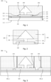
- Figure 1 shows a heteroepitaxial semiconductor device 100 which comprises a bulk semiconductor substrate 110, a seed layer 120, a separation layer 130, a heteroepitaxial structure 140 and a dielectric material layer 150.
- the seed layer 120 comprises or consists of a first semiconductor material.
- the seed layer 120 may be a crystalline seed layer.
- the seed layer 120 is arranged at a first side 111 of the bulk semiconductor substrate 110 such that a first side 121 of the seed layer 120 faces the bulk semiconductor substrate 110 and an opposing second side 122 faces away from the bulk semiconductor substrate 110.
- the seed layer 120 furthermore comprises lateral sides 123 connecting the first and second sides 121, 122.
- the seed layer 120 may have any suitable dimensions.
- the seed layer 120 may have a thickness measured between the first and second sides 121, 122 of 1 ⁇ m or less, or 500nm or less, or 100nm or less, or 50nm or less, or 20nm or less, or 10nm or less.
- the seed layer 120 may e.g. have a lateral extension measured between opposing lateral sides 123 of 100 ⁇ m or less, or 50 ⁇ m or less, or 10 ⁇ m or less, or 5 ⁇ m or less. As shown in Fig. 1 , the lateral extension of the seed layer 120 may be larger than a maximum lateral extension of the heteroepitaxial structure 140.
- the lateral extension of the seed layer 120 is smaller than the maximum lateral extension of the heteroepitaxial structure 140 (but still at least as large as the lateral extension of a trunk portion 141 of the heteroepitaxial structure 140). It is also possible that the seed layer 120 has a rectangular shape such that along its longer side it is larger than the heteroepitaxial structure 140 but along its shorter side it is smaller.
- the lateral sides 123 of the seed layer 120 may be recessed from lateral sides of the heteroepitaxial semiconductor device 100. Minimizing the lateral dimensions of the seed layer 120 in this manner may help with reducing stress and/or dislocations and defects in the heteroepitaxial structure 140. For this reason, a larger heteroepitaxial structure 140 and/or a heteroepitaxial structure 140 with less dislocations and crystal defects may be grown on the seed layer 120 compared to a seed layer with larger lateral dimensions.
- the bulk semiconductor substrate 110 may e.g. be a semiconductor wafer or a singulated semiconductor die.
- the bulk semiconductor substrate 110 may comprise or consist of the first semiconductor material.
- the bulk semiconductor substrate 110 may comprise a second side 112 opposite the first side 111 and it may comprise lateral sides 113 connecting the first and second sides 111, 112.
- the lateral sides 113 may for example be cut surfaces or there may be further heteroepitaxial semiconductor devices 100 arranged laterally next to the single device shown in the example of Fig. 1 .
- the bulk semiconductor substrate 110 may have any suitable dimensions.
- the bulk semiconductor substrate 110 may have a thickness measured between the first and second sides 111, 112 of 50 ⁇ m or more, 100 ⁇ m or more, 200 ⁇ m or more, 500 ⁇ m or more, or 1mm or more.
- the separation layer 130 is arranged between the bulk semiconductor substrate 110 and the seed layer 120.
- the separation layer 130 may be configured to electrically insulate the seed layer 120 from the bulk semiconductor substrate 110.
- the seed layer 120 may also be termed a "silicon on insulator" (SOI) layer.
- SOI silicon on insulator
- the separation layer 130 may for example be a dielectric material layer, e.g. an oxide layer ("buried oxide layer”).
- the buried oxide layer may e.g. be a silicon oxide layer.
- the separation layer 130 may comprise a cavity within the bulk semiconductor substrate, wherein the seed layer 120 is arranged above the cavity. In this case, the seed layer 120 may also be termed a "silicon on nothing" (SON) layer.
- SON silicon on nothing
- the separation layer 130 may have any suitable thickness, for example a thickness of 1 ⁇ m or less, or 500nm or less, or 100nm or less, or 50nm or less.
- the heteroepitaxial structure 140 is grown on the second side 122 of the seed layer 120 and it comprises or consists of a second semiconductor material, different from the first semiconductor material.
- the first and second semiconductor materials may be any suitable semiconductor materials.
- the first and second semiconductor materials may have similar lattice constants and/or similar thermal expansion coefficients.
- the first semiconductor material is Si and the second semiconductor material is Ge.
- the heteroepitaxial structure 140 may have any suitable shape and any suitable dimensions.
- the particular shape of the heteroepitaxial structure 140 is a product of self-organization during epitaxial growth.
- methods like aspect ratio trapping (ART) may be used to grow an essentially defect free heteroepitaxial structure 140 of a particular shape.
- the dielectric material layer 150 is arranged on the seed layer 120, in particular such that it also (completely) covers the lateral sides 123 of the seed layer 120.
- the dielectric material layer 150 may completely cover all lateral sides 123 of the seed layer 120.
- the dielectric material layer 150 at least partially encapsulates the heteroepitaxial structure 140.
- the dielectric material layer 150 may for example encapsulate all lateral sides of the heteroepitaxial structure 140.
- the dielectric material layer 150 is an oxide layer.
- the oxide layer may e.g. comprise an oxide of the first semiconductor material of the seed layer 120 or an oxide of the semiconductor material of the bulk semiconductor substrate 110.
- the oxide layer may for example comprise a silicon oxide.
- Figure 2 shows a detail view of the heteroepitaxial structure 140, the seed layer 120 and the dielectric material layer 150 of Fig. 1 , according to an example.
- the heteroepitaxial structure 140 comprises a trunk portion 141 and a top portion 142 arranged on top of the trunk portion 141. Both the trunk portion 141 and the top portion 142 may be part of a contiguous single piece heteroepitaxial structure 140 and may only be distinguished by their different shapes.
- the trunk portion 141 may be grown directly on the second side 122 of the seed layer 120.
- the dielectric material layer 150 may comprise a layer stack, for example comprising a lower dielectric material layer 151 and an upper dielectric material layer 152.
- the trunk portion 141 of the heteroepitaxial structure 140 may be arranged in an aperture in the lower dielectric material layer 151 and the top portion of the heteroepitaxial structure 140 may be arranged in the upper dielectric material layer 152.
- the dielectric material layer 150 may also comprise a (third) bottom dielectric material layer, wherein the laterals sides 123 of the seed layer 120 are covered by the bottom dielectric material layer and the lower dielectric material layer 151 is arranged on the bottom dielectric material layer and covers the second side 122 of the seed layer 120 and the trunk portion 141 of the heteroepitaxial structure 140.
- the individual layers which form the dielectric material layer 150 may all comprise or consist of the same material or material composition or individual layers may comprise or consist of different materials or material compositions.
- the lower dielectric material layer 151 with the aperture may be fabricated on the seed layer 120 prior to growing the heteroepitaxial structure 140, in particular in order to be used for aspect ratio trapping.
- the heteroepitaxial structure 140 may be grown in the aperture, wherein dislocations in the heteroepitaxial structure 140 are trapped in the aperture in the lower dielectric material layer 151 due to their propagation diagonal to the direction of growth.
- the heteroepitaxial structure 140, in particular the top portion 142 may therefore be essentially free of crystal dislocations.
- the trunk portion 141 may have a high aspect ratio.
- the trunk portion 141 may have an aspect ratio in the range of 1:1 to 10, for example about 1:2, or 1:4, or 1:6, or 1:8. It is however also possible that a lower aspect ratio is used, for example 2:1, 3:1, 10:1, 30:1, or even 100:1. Generally speaking, the aspect ratio may be anywhere in the range of 100:1 to 1:100.
- a cross section of the trunk portion 141 as shown in Fig. 2 may essentially have a rectangular shape. In a sectional view onto a plane parallel to the second side 122 of the seed layer, the trunk portion 141 may for example have a circular shape, a quadratic shape or a rectangular shape.
- aspects ratio trapping refers to techniques of stopping defects with non-crystalline sidewalls of sufficient height relative to the size of the crystalline growth area.
- the approach for fabricating e.g. the semiconductor device 100 disclosed herein may comprise reducing the dislocation density of a lattice mismatched heteroepitaxial grown material by lattice adaption between the seed layer 120 and the epitaxially grown material (i.e. the heteroepitaxial structure 140), in particular by allowing more lattice adaption in the seed layer 120.
- the trunk portion 141 may for example have a lateral extension (a width of the aperture in the lower dielectric material layer 151) of 1 ⁇ m or less, or 500nm or less, or 200nm or less, or 100nm or less, or 50nm or less.
- the top portion 142 may for example have a cone shape or pyramid shape as shown in Fig. 2 . However, the top portion 142 may for example also have a rectangular shape, an inverse cone shape, etc. According to an example, an upper surface of the top portion 142 is exposed from the dielectric material layer 150, e.g. by use of a chemical mechanical polishing (CMP) process. According to another example, the upper surface of the top portion 142 is covered by the dielectric material layer 150.
- CMP chemical mechanical polishing
- a maximum lateral extension of the top portion 142 may for example be 10 ⁇ m or less, or 5 ⁇ m or less, or 2 ⁇ m or less, or 1 ⁇ m or less.
- the top portion 142 may have a height (which may be equal to a thickness of the upper dielectric material layer 152) of for example 2 ⁇ m or less, or 1 ⁇ m or less, or 500nm or less, or 200nm or less.
- Fabricating the heteroepitaxial semiconductor device 100 may comprise arranging the lower dielectric material layer 151 on the seed layer 120, fabricating an aperture in the lower dielectric material layer 151, growing the trunk portion 141 in the aperture and the top portion 142 on top of the trunk portion 141 and on top of the lower dielectric material layer 151, and arranging the upper dielectric material layer 152 on top of the lower dielectric material layer 151 and on the top portion 142 of the heteroepitaxial structure 140.
- Figure 3 shows a further heteroepitaxial semiconductor device 300 which may be similar to or identical with the heteroepitaxial semiconductor device 100.
- the heteroepitaxial semiconductor device 300 may comprise all parts discussed with respect to Figs. 1 and 2 and it may additionally comprise further seed layers 120_1 and 120_2 arranged laterally next to the seed layer 120.
- the seed layer 120 may be separated from the further seed layers 120_1, 120_2 by gaps 310.
- the further seed layers 120_1 and 120_2 may have the same dimensions and/or the same material composition as the seed layer 120.
- the seed layer 120 and the further seed layers 120_1, 120_2 are fabricated in the same fabrication process.
- a single common seed layer may be fabricated on top of the separation layer 130 and afterwards the gaps 310 separating the seed layers 120, 120_1 and 120_2 from each other may be generated.
- the seed layers 120, 120_1 and 120_2 may be separate parts of a common seed layer on top of the separation layer 130.
- the gaps 310 may be configured to physically and electrically isolate the seed layers 120, 120_1, and 120_2 from each other.
- the gaps 310 may be filled by the dielectric material layer 150.
- the gaps 310 may have any suitable dimensions, e.g. a width measured between adjacent one of the seed layers 120, 120_1 and 120_2 of 100nm or more, 200nm or more, 500nm or more, 1 ⁇ m or more, or 2 ⁇ m or more.
- the heteroepitaxial semiconductor device 300 may further comprise one or more transistor or diode structures.
- the transistor or diode structures may be arranged at the seed layer 120.
- the transistor or diode structures may comprise poly gates 320 arranged on the seed layer 120.
- the heteroepitaxial semiconductor device 300 may further comprise contacts 330 configured to electrically contact the poly gates 320.
- the contacts 330 may be arranged in the dielectric material layer 150, laterally next to the heteroepitaxial structure 140.
- the heteroepitaxial semiconductor devices 100 and 300 may be part of any suitable electronic device, for example part of an image sensor.
- the heteroepitaxial semiconductor devices 100 and 300 may in particular be part of a time of flight image sensor, e.g. a photonic mixing device (PMD).
- PMD photonic mixing device
- the heteroepitaxial structure 140 may form a photosensitive part of a pixel of the image sensor.
- An electronic pixel read out part configured to read out the pixel may be arranged laterally next to the heteroepitaxial structure 140.
- the electronic pixel read out part may e.g. be arranged at the further seed layers 120_1, 120_2.
- Figures 4A and 4B show a further heteroepitaxial semiconductor device 400 which may be similar to or identical with the heteroepitaxial semiconductor device 100 or 300, except for the differences described in the following.
- Fig. 4A shows a sectional view and Fig. 4B shows a top view.
- the bulk semiconductor substrate 110 in particular the first side 111 of the bulk semiconductor substrate 110, comprises a depression 410 and the separation layer 130 and the seed layer 120 are arranged within the depression 410.
- the depression 410 may have any suitable dimensions.
- the depression 410 may have a depth d that is smaller than or as large as or larger than a combined thickness of the seed layer 120 and the separation layer 130.
- the depth d may for example be 100nm or more, or 200nm or more, or 500nm or more.
- the depression 410 may have a rectangular shape.
- a length 1 of the depression 410 may be larger than a maximum lateral extension of the heteroepitaxial structure 140.
- the length 1 may for example be 1 ⁇ m or more, or 2 ⁇ m or more, or 3 ⁇ m or more, or 5 ⁇ m or more.
- a width w of the depression 410 may for example be about no more than half of the length 1, or no more than one quarter of the length 1.
- the depression 410 has a quadratic shape, a circular shape, etc.
- a bottom of the depression 410 may be completely covered by the separation layer 130.
- the lateral sides 123 of the seed layer 120 may be recessed with respect to lateral sides of the depression 410 such that a gap 310 completely surrounds the seed layer 120 laterally.
- the heteroepitaxial semiconductor device 400 comprises diode structures 320_1 and transistor structures 320_2, wherein the diode structures 320_1 are arranged at the seed layer 120 and the transistor structures 320_2 are arranged at the first side 111 of the bulk semiconductor substrate 110, laterally next to the depression 410.
- the diode structures 320_1 may be part of a pixel and the transistor structures 320_2 may be part of a pixel read out structure.
- Figures 5A to 5F show the heteroepitaxial semiconductor device 300 in various stages of fabrication, according to an exemplary method for fabricating semiconductor devices. Comparable methods may be used for fabricating the heteroepitaxial semiconductor devices 100 and 400.
- the bulk semiconductor substrate 110 with the separation layer 130 and the seed layer 120 is provided.
- the lateral extension of the seed layer 120 is limited by the gap 310 which may completely surround the seed layer 120.
- the gap 310 may for example be provided by locally removing the seed layer 120 (e.g. by etching) or by fabricating the seed layer 120 on the separation layer 130 in a predefined pattern.
- Providing the separation layer 130 may comprise generating a buried oxide layer or a cavity in the bulk semiconductor substrate 110.
- a transistor structure e.g. of the CMOS type, may be fabricated at the seed layer 120. This may also comprise fabricating the poly gates 320 which may e.g. be configured to provide one or more gates, e.g. separation gates and modulation gates for a pixel of an image sensor, diode contacts, ground contacts, etc.
- the poly gates 320 may e.g. be configured to provide one or more gates, e.g. separation gates and modulation gates for a pixel of an image sensor, diode contacts, ground contacts, etc.
- the lower dielectric material layer 151 comprising an aperture 153 is applied on top of the seed layer 120.
- Providing the aperture 153 may comprise locally removing the dielectric material layer 151.
- the heteroepitaxial structure 140 is grown on the seed layer 120, beginning in the aperture 153.
- This may in particular comprise a selective epitaxial growth process.
- the epitaxial growth process may comprise alternating depositing and etching back steps. Dislocations in the crystalline structure of the heteroepitaxial structure 140 are trapped within the aperture.
- the comparatively small lateral extension of the seed layer 120 and/or its comparatively small thickness may help with reducing stress in the seed layer 120.
- the comparatively small area of contact between the seed layer 120 and the heteroepitaxial structure 140 (which is due to the narrowness of the aperture 153) may help with minimizing the stress that is induced into the heteroepitaxial structure 140. All these factors may reduce or eliminate dislocations in the heteroepitaxial structure 140.
- the upper dielectric material layer 152 is applied on top of the lower dielectric material layer 151 and the heteroepitaxial structure 140.
- an optional CMP process may be used to expose a flattened top surface 143 of the heteroepitaxial structure 140. Furthermore, the contacts 330 may be fabricated.
- Figure 6 is a flow chart of an exemplary method 600 for fabricating a heteroepitaxial semiconductor device.
- the method 600 may for example be used for fabricating the heteroepitaxial semiconductor devices 100, 300 and 400.
- the method 600 comprises at 601 an act of providing a substrate, the substrate comprising a bulk semiconductor substrate, a separation layer arranged on the bulk semiconductor substrate and a seed layer of a first semiconductor material arranged on the separation layer, wherein the seed layer comprises a first side facing the bulk semiconductor substrate, an opposing second side and lateral sides connecting the first and second sides, at 602 an act of depositing a dielectric material layer on the seed layer such that the dielectric material layer covers the second side and the lateral sides of the seed layer, at 603 an act of generating a hole in the dielectric material layer such that the second side of the seed layer is exposed in the hole, and at 604 an act of growing a heteroepitaxial structure of a second semiconductor material, different from the first semiconductor material, on the seed layer, starting in the hole.
- the method 600 comprises an optional act of fabricating semiconductor transistor circuitry on the substrate prior to growing the heteroepitaxial structure.
- heteroepitaxial semiconductor device and the method for fabricating a heteroepitaxial semiconductor device are further described using specific examples.
- Example 1 is a heteroepitaxial semiconductor device, comprising: a bulk semiconductor substrate, a seed layer comprising a first semiconductor material, the seed layer being arranged at a first side of the bulk semiconductor substrate and comprising a first side facing the bulk semiconductor substrate, an opposing second side and lateral sides connecting the first and second sides, a separation layer arranged between the bulk semiconductor substrate and the seed layer, a heteroepitaxial structure grown on the second side of the seed layer and comprising a second semiconductor material, different from the first semiconductor material, and a dielectric material layer arranged on the seed layer and at least partially encapsulating the heteroepitaxial structure, wherein the dielectric material layer also covers the lateral sides of the seed layer.
- Example 2 is the heteroepitaxial semiconductor device of example 1, wherein the heteroepitaxial structure comprises a trunk portion connected to the seed layer and a top portion arranged on top of the trunk portion, wherein a lateral extension of the trunk portion is smaller than a lateral extension of the top portion, the lateral extensions being measured parallel to the second side of the seed layer.
- Example 3 is the heteroepitaxial semiconductor device of example 2, wherein the dielectric material layer comprises a lower dielectric material layer and an upper dielectric material layer, wherein the trunk portion is arranged within the lower dielectric material layer and the top portion is arranged within the upper dielectric material layer.
- Example 4 is the heteroepitaxial semiconductor device of example 2 or 3, wherein the top portion has an essentially pyramidal shape.
- Example 5 is the heteroepitaxial semiconductor device of one of examples 2 to 4, wherein the trunk portion has an aspect ratio in the range of 100:1 to 1:100, in particular in the range of 1:1 to 1:10.
- Example 6 is the heteroepitaxial semiconductor device of one of the preceding examples, wherein the seed layer has lateral dimensions measured parallel to the second side of the seed layer of 10 ⁇ m or less, in particular 5 ⁇ m or less.
- Example 7 is the heteroepitaxial semiconductor device of one of the preceding examples, wherein the first semiconductor material is Si and the second semiconductor material is Ge.
- Example 8 is the heteroepitaxial semiconductor device of one of the preceding examples, wherein the separation layer comprises a buried dielectric material layer or a cavity within the bulk semiconductor substrate.
- Example 9 is the heteroepitaxial semiconductor device of one of the preceding examples, wherein the bulk semiconductor substrate comprises a depression and wherein the separation layer and the seed layer are arranged within the depression.
- Example 10 is an image sensor, comprising: a heteroepitaxial semiconductor device according to one of the preceding examples, wherein the heteroepitaxial structure forms a photosensitive part of a pixel of the image sensor.
- Example 11 is the image sensor of example 10, wherein the image sensor is a time of flight image sensor comprising a photonic mixer device.
- Example 12 is the image sensor of example 10 or 11, further comprising: an electronic pixel read out part arranged laterally next to the heteroepitaxial semiconductor device and configured to read out the pixel, wherein the read out part comprises a further seed layer arranged coplanar with the seed layer and laterally at a distance from the seed layer.
- Example 13 is a method for fabricating a heteroepitaxial semiconductor device, the method comprising: providing a substrate, the substrate comprising a bulk semiconductor substrate, a separation layer arranged on the bulk semiconductor substrate and a seed layer of a first semiconductor material arranged on the separation layer, wherein the seed layer comprises a first side facing the bulk semiconductor substrate, an opposing second side and lateral sides connecting the first and second sides, depositing a dielectric material layer on the seed layer such that the dielectric material layer covers the second side and the lateral sides of the seed layer, generating a hole in the dielectric material layer such that the second side of the seed layer is exposed in the hole, and growing a heteroepitaxial structure of a second semiconductor material, different from the first semiconductor material, on the seed layer, starting in the hole.
- Example 14 is the method of example 13, wherein the dielectric material layer comprises a lower dielectric material layer and an upper dielectric material layer, wherein the hole is arranged in the lower dielectric material layer, and wherein the upper dielectric material layer is deposited on the lower dielectric material layer after the heteroepitaxial structure has been grown.
- Example 15 is the method of example 13 or 14, further comprising: fabricating semiconductor transistor circuitry on the substrate prior to growing the heteroepitaxial structure.
- Example 16 is an apparatus with means for performing the method according to anyone of examples 13 to 15.
Landscapes
- Recrystallisation Techniques (AREA)
Abstract
Description
- This disclosure relates in general to a heteroepitaxial semiconductor device, for example to a heteroepitaxial semiconductor device which may be used in an image sensor, as well as to a method for fabricating the same.
- A heteroepitaxial semiconductor device comprises a seed layer and a structure epitaxially grown on the seed layer, wherein the seed layer and the structure are comprised of different semiconductor compounds. For example, a Ge layer may be epitaxially grown on a Si seed layer. The two different semiconductor compounds may have similar lattice constants and/or thermal expansion coefficients. It may be desirable to fabricate heteroepitaxial layers of a particularly large size and/or with particularly few crystal defects. However, dislocations which may originate from the boundary between the seed layer and the heteroepitaxial layer may set an upper limit for the size and/or the flawlessness of the crystal structure of the heteroepitaxial layer. Improved heteroepitaxial semiconductor devices and improved methods for fabricating heteroepitaxial semiconductor devices may reduce or even eliminate these dislocations and may also provide further benefits.
- The problem on which the invention is based is solved by the features of the independent claims. Further advantageous examples are described in the dependent claims.
- Various aspects pertain to a heteroepitaxial semiconductor device, comprising: a bulk semiconductor substrate, a seed layer comprising a first semiconductor material, the seed layer being arranged at a first side of the bulk semiconductor substrate and comprising a first side facing the bulk semiconductor substrate, an opposing second side and lateral sides connecting the first and second sides, a separation layer arranged between the bulk semiconductor substrate and the seed layer, a heteroepitaxial structure grown on the second side of the seed layer and comprising a second semiconductor material, different from the first semiconductor material, and a dielectric material layer arranged on the seed layer and at least partially encapsulating the heteroepitaxial structure, wherein the dielectric material layer also covers the lateral sides of the seed layer.
- Various aspects pertain to a method for fabricating a heteroepitaxial semiconductor device, the method comprising: providing a substrate, the substrate comprising a bulk semiconductor substrate, a separation layer arranged on the bulk semiconductor substrate and a seed layer of a first semiconductor material arranged on the separation layer, wherein the seed layer comprises a first side facing the bulk semiconductor substrate, an opposing second side and lateral sides connecting the first and second sides, depositing a dielectric material layer on the seed layer such that the dielectric material layer covers the second side and the lateral sides of the seed layer, generating a hole in the dielectric material layer such that the second side of the seed layer is exposed in the hole, and growing a heteroepitaxial structure of a second semiconductor material, different from the first semiconductor material, on the seed layer, starting in the hole.
- The accompanying drawings illustrate examples and together with the description serve to explain principles of the disclosure. Other examples and many of the intended advantages of the disclosure will be readily appreciated in view of the following detailed description. The elements of the drawings are not necessarily to scale relative to each other. Identical reference numerals designate corresponding similar parts.
-
Figure 1 is a sectional view of a heteroepitaxial semiconductor device, wherein a dielectric material layer encapsulates lateral sides of a seed layer. -
Figure 2 is a detail view of the heteroepitaxial structure and the seed layer of the device ofFig. 1 . -
Figure 3 is a sectional view of a further heteroepitaxial semiconductor device, wherein the seed layer is laterally delimited by a gap filled with dielectric material. -
Figures 4A and 4B are a sectional view and a top view of a further heteroepitaxial semiconductor device, wherein the seed layer is arranged within a depression in the bulk semiconductor substrate. -
Figures 5A to 5F show a heteroepitaxial semiconductor device in various stages of fabrication according to an exemplary method for fabricating heteroepitaxial semiconductor devices. -
Figure 6 is a flow chart of an exemplary method for fabricating heteroepitaxial semiconductor devices. - In the following detailed description, directional terminology, such as "top", "bottom", "left", "right", "upper", "lower" etc., is used with reference to the orientation of the Figure(s) being described. Because components of the disclosure can be positioned in a number of different orientations, the directional terminology is used for purposes of illustration only.
- In addition, while a particular feature or aspect of an example may be disclosed with respect to only one of several implementations, such feature or aspect may be combined with one or more other features or aspects of the other implementations as may be desired and advantageous for any given or particular application, unless specifically noted otherwise or unless technically restricted. Furthermore, to the extent that the terms "include", "have", "with" or other variants thereof are used in either the detailed description or the claims, such terms are intended to be inclusive in a manner similar to the term "comprise". Also, the term "exemplary" is merely meant as an example, rather than the best or optimal.
- In several examples layers or layer stacks are applied to one another or materials are applied or deposited onto layers. It should be appreciated that any such terms as "applied" or "deposited" are meant to cover literally all kinds and techniques of applying layers onto each other.
- An efficient heteroepitaxial semiconductor device may for example reduce material consumption, ohmic losses, chemical waste etc. and may thus enable energy and/or resource savings. Improved heteroepitaxial semiconductor device, as specified in this description, may thus at least indirectly contribute to green technology solutions, i.e. climate-friendly solutions providing a mitigation of energy and/or resource use.
-
Figure 1 shows aheteroepitaxial semiconductor device 100 which comprises abulk semiconductor substrate 110, aseed layer 120, aseparation layer 130, aheteroepitaxial structure 140 and adielectric material layer 150. - The
seed layer 120 comprises or consists of a first semiconductor material. Theseed layer 120 may be a crystalline seed layer. Theseed layer 120 is arranged at afirst side 111 of thebulk semiconductor substrate 110 such that afirst side 121 of theseed layer 120 faces thebulk semiconductor substrate 110 and an opposingsecond side 122 faces away from thebulk semiconductor substrate 110. Theseed layer 120 furthermore compriseslateral sides 123 connecting the first andsecond sides - The
seed layer 120 may have any suitable dimensions. For example, theseed layer 120 may have a thickness measured between the first andsecond sides seed layer 120 may e.g. have a lateral extension measured between opposinglateral sides 123 of 100µm or less, or 50µm or less, or 10µm or less, or 5µm or less. As shown inFig. 1 , the lateral extension of theseed layer 120 may be larger than a maximum lateral extension of theheteroepitaxial structure 140. However, it is also possible that the lateral extension of theseed layer 120 is smaller than the maximum lateral extension of the heteroepitaxial structure 140 (but still at least as large as the lateral extension of atrunk portion 141 of the heteroepitaxial structure 140). It is also possible that theseed layer 120 has a rectangular shape such that along its longer side it is larger than theheteroepitaxial structure 140 but along its shorter side it is smaller. - As shown in
Fig. 1 , thelateral sides 123 of theseed layer 120 may be recessed from lateral sides of theheteroepitaxial semiconductor device 100. Minimizing the lateral dimensions of theseed layer 120 in this manner may help with reducing stress and/or dislocations and defects in theheteroepitaxial structure 140. For this reason, a largerheteroepitaxial structure 140 and/or aheteroepitaxial structure 140 with less dislocations and crystal defects may be grown on theseed layer 120 compared to a seed layer with larger lateral dimensions. - The
bulk semiconductor substrate 110 may e.g. be a semiconductor wafer or a singulated semiconductor die. Thebulk semiconductor substrate 110 may comprise or consist of the first semiconductor material. Thebulk semiconductor substrate 110 may comprise asecond side 112 opposite thefirst side 111 and it may compriselateral sides 113 connecting the first andsecond sides lateral sides 113 may for example be cut surfaces or there may be furtherheteroepitaxial semiconductor devices 100 arranged laterally next to the single device shown in the example ofFig. 1 . - The
bulk semiconductor substrate 110 may have any suitable dimensions. For example, thebulk semiconductor substrate 110 may have a thickness measured between the first andsecond sides - The
separation layer 130 is arranged between thebulk semiconductor substrate 110 and theseed layer 120. Theseparation layer 130 may be configured to electrically insulate theseed layer 120 from thebulk semiconductor substrate 110. For this reason, theseed layer 120 may also be termed a "silicon on insulator" (SOI) layer. Theseparation layer 130 may for example be a dielectric material layer, e.g. an oxide layer ("buried oxide layer"). The buried oxide layer may e.g. be a silicon oxide layer. According to another example, theseparation layer 130 may comprise a cavity within the bulk semiconductor substrate, wherein theseed layer 120 is arranged above the cavity. In this case, theseed layer 120 may also be termed a "silicon on nothing" (SON) layer. - The
separation layer 130 may have any suitable thickness, for example a thickness of 1µm or less, or 500nm or less, or 100nm or less, or 50nm or less. - The
heteroepitaxial structure 140 is grown on thesecond side 122 of theseed layer 120 and it comprises or consists of a second semiconductor material, different from the first semiconductor material. The first and second semiconductor materials may be any suitable semiconductor materials. The first and second semiconductor materials may have similar lattice constants and/or similar thermal expansion coefficients. According to an example, the first semiconductor material is Si and the second semiconductor material is Ge. - The
heteroepitaxial structure 140 may have any suitable shape and any suitable dimensions. According to an example, the particular shape of theheteroepitaxial structure 140 is a product of self-organization during epitaxial growth. According to an example, methods like aspect ratio trapping (ART) may be used to grow an essentially defect freeheteroepitaxial structure 140 of a particular shape. - The
dielectric material layer 150 is arranged on theseed layer 120, in particular such that it also (completely) covers thelateral sides 123 of theseed layer 120. Thedielectric material layer 150 may completely cover alllateral sides 123 of theseed layer 120. Thedielectric material layer 150 at least partially encapsulates theheteroepitaxial structure 140. Thedielectric material layer 150 may for example encapsulate all lateral sides of theheteroepitaxial structure 140. - According to an example, the
dielectric material layer 150 is an oxide layer. The oxide layer may e.g. comprise an oxide of the first semiconductor material of theseed layer 120 or an oxide of the semiconductor material of thebulk semiconductor substrate 110. The oxide layer may for example comprise a silicon oxide. -
Figure 2 shows a detail view of theheteroepitaxial structure 140, theseed layer 120 and thedielectric material layer 150 ofFig. 1 , according to an example. - According to the example shown in
Fig. 2 , theheteroepitaxial structure 140 comprises atrunk portion 141 and atop portion 142 arranged on top of thetrunk portion 141. Both thetrunk portion 141 and thetop portion 142 may be part of a contiguous single pieceheteroepitaxial structure 140 and may only be distinguished by their different shapes. Thetrunk portion 141 may be grown directly on thesecond side 122 of theseed layer 120. - As shown in
Fig. 2 , thedielectric material layer 150 may comprise a layer stack, for example comprising a lowerdielectric material layer 151 and an upperdielectric material layer 152. Thetrunk portion 141 of theheteroepitaxial structure 140 may be arranged in an aperture in the lowerdielectric material layer 151 and the top portion of theheteroepitaxial structure 140 may be arranged in the upperdielectric material layer 152. According to an example, thedielectric material layer 150 may also comprise a (third) bottom dielectric material layer, wherein the laterals sides 123 of theseed layer 120 are covered by the bottom dielectric material layer and the lowerdielectric material layer 151 is arranged on the bottom dielectric material layer and covers thesecond side 122 of theseed layer 120 and thetrunk portion 141 of theheteroepitaxial structure 140. The individual layers which form thedielectric material layer 150 may all comprise or consist of the same material or material composition or individual layers may comprise or consist of different materials or material compositions. - The lower
dielectric material layer 151 with the aperture may be fabricated on theseed layer 120 prior to growing theheteroepitaxial structure 140, in particular in order to be used for aspect ratio trapping. Theheteroepitaxial structure 140 may be grown in the aperture, wherein dislocations in theheteroepitaxial structure 140 are trapped in the aperture in the lowerdielectric material layer 151 due to their propagation diagonal to the direction of growth. Theheteroepitaxial structure 140, in particular thetop portion 142, may therefore be essentially free of crystal dislocations. - In order to trap said dislocations, the trunk portion 141 (or rather the aperture in the lower dielectric material layer 151) may have a high aspect ratio. For example, the
trunk portion 141 may have an aspect ratio in the range of 1:1 to 10, for example about 1:2, or 1:4, or 1:6, or 1:8. It is however also possible that a lower aspect ratio is used, for example 2:1, 3:1, 10:1, 30:1, or even 100:1. Generally speaking, the aspect ratio may be anywhere in the range of 100:1 to 1:100. Furthermore, a cross section of thetrunk portion 141 as shown inFig. 2 may essentially have a rectangular shape. In a sectional view onto a plane parallel to thesecond side 122 of the seed layer, thetrunk portion 141 may for example have a circular shape, a quadratic shape or a rectangular shape. - Aspect ratio trapping, as it may, according to an example, be used for fabricating the
semiconductor 100, refers to techniques of stopping defects with non-crystalline sidewalls of sufficient height relative to the size of the crystalline growth area. In place of aspect ratio trapping or in addition to it, the approach for fabricating e.g. thesemiconductor device 100 disclosed herein may comprise reducing the dislocation density of a lattice mismatched heteroepitaxial grown material by lattice adaption between theseed layer 120 and the epitaxially grown material (i.e. the heteroepitaxial structure 140), in particular by allowing more lattice adaption in theseed layer 120. - The
trunk portion 141 may for example have a lateral extension (a width of the aperture in the lower dielectric material layer 151) of 1µm or less, or 500nm or less, or 200nm or less, or 100nm or less, or 50nm or less. - The
top portion 142 may for example have a cone shape or pyramid shape as shown inFig. 2 . However, thetop portion 142 may for example also have a rectangular shape, an inverse cone shape, etc. According to an example, an upper surface of thetop portion 142 is exposed from thedielectric material layer 150, e.g. by use of a chemical mechanical polishing (CMP) process. According to another example, the upper surface of thetop portion 142 is covered by thedielectric material layer 150. - A maximum lateral extension of the
top portion 142 may for example be 10µm or less, or 5µm or less, or 2µm or less, or 1µm or less. Thetop portion 142 may have a height (which may be equal to a thickness of the upper dielectric material layer 152) of for example 2µm or less, or 1µm or less, or 500nm or less, or 200nm or less. - Fabricating the
heteroepitaxial semiconductor device 100 may comprise arranging the lowerdielectric material layer 151 on theseed layer 120, fabricating an aperture in the lowerdielectric material layer 151, growing thetrunk portion 141 in the aperture and thetop portion 142 on top of thetrunk portion 141 and on top of the lowerdielectric material layer 151, and arranging the upperdielectric material layer 152 on top of the lowerdielectric material layer 151 and on thetop portion 142 of theheteroepitaxial structure 140. -
Figure 3 shows a furtherheteroepitaxial semiconductor device 300 which may be similar to or identical with theheteroepitaxial semiconductor device 100. - The
heteroepitaxial semiconductor device 300 may comprise all parts discussed with respect toFigs. 1 and 2 and it may additionally comprise further seed layers 120_1 and 120_2 arranged laterally next to theseed layer 120. Theseed layer 120 may be separated from the further seed layers 120_1, 120_2 bygaps 310. - The further seed layers 120_1 and 120_2 may have the same dimensions and/or the same material composition as the
seed layer 120. According to an example, theseed layer 120 and the further seed layers 120_1, 120_2 are fabricated in the same fabrication process. For example, a single common seed layer may be fabricated on top of theseparation layer 130 and afterwards thegaps 310 separating the seed layers 120, 120_1 and 120_2 from each other may be generated. In other words, the seed layers 120, 120_1 and 120_2 may be separate parts of a common seed layer on top of theseparation layer 130. - The
gaps 310 may be configured to physically and electrically isolate the seed layers 120, 120_1, and 120_2 from each other. Thegaps 310 may be filled by thedielectric material layer 150. Thegaps 310 may have any suitable dimensions, e.g. a width measured between adjacent one of the seed layers 120, 120_1 and 120_2 of 100nm or more, 200nm or more, 500nm or more, 1µm or more, or 2µm or more. - The
heteroepitaxial semiconductor device 300 may further comprise one or more transistor or diode structures. The transistor or diode structures may be arranged at theseed layer 120. The transistor or diode structures may comprisepoly gates 320 arranged on theseed layer 120. Theheteroepitaxial semiconductor device 300 may further comprisecontacts 330 configured to electrically contact thepoly gates 320. Thecontacts 330 may be arranged in thedielectric material layer 150, laterally next to theheteroepitaxial structure 140. - The
heteroepitaxial semiconductor devices heteroepitaxial semiconductor devices - In the case that the
heteroepitaxial semiconductor device heteroepitaxial structure 140 may form a photosensitive part of a pixel of the image sensor. An electronic pixel read out part configured to read out the pixel may be arranged laterally next to theheteroepitaxial structure 140. The electronic pixel read out part may e.g. be arranged at the further seed layers 120_1, 120_2. -
Figures 4A and 4B show a furtherheteroepitaxial semiconductor device 400 which may be similar to or identical with theheteroepitaxial semiconductor device Fig. 4A shows a sectional view andFig. 4B shows a top view. - In the
heteroepitaxial semiconductor device 400 thebulk semiconductor substrate 110, in particular thefirst side 111 of thebulk semiconductor substrate 110, comprises adepression 410 and theseparation layer 130 and theseed layer 120 are arranged within thedepression 410. - The
depression 410 may have any suitable dimensions. For example, thedepression 410 may have a depth d that is smaller than or as large as or larger than a combined thickness of theseed layer 120 and theseparation layer 130. The depth d may for example be 100nm or more, or 200nm or more, or 500nm or more. According to an example, thedepression 410 may have a rectangular shape. A length 1 of thedepression 410 may be larger than a maximum lateral extension of theheteroepitaxial structure 140. The length 1 may for example be 1µm or more, or 2µm or more, or 3µm or more, or 5µm or more. A width w of thedepression 410 may for example be about no more than half of the length 1, or no more than one quarter of the length 1. According to another example, thedepression 410 has a quadratic shape, a circular shape, etc. - A bottom of the
depression 410 may be completely covered by theseparation layer 130. The lateral sides 123 of theseed layer 120 may be recessed with respect to lateral sides of thedepression 410 such that agap 310 completely surrounds theseed layer 120 laterally. - According to an example, the
heteroepitaxial semiconductor device 400 comprises diode structures 320_1 and transistor structures 320_2, wherein the diode structures 320_1 are arranged at theseed layer 120 and the transistor structures 320_2 are arranged at thefirst side 111 of thebulk semiconductor substrate 110, laterally next to thedepression 410. In the case that theheteroepitaxial semiconductor device 400 is part of an image sensor, the diode structures 320_1 may be part of a pixel and the transistor structures 320_2 may be part of a pixel read out structure. -
Figures 5A to 5F show theheteroepitaxial semiconductor device 300 in various stages of fabrication, according to an exemplary method for fabricating semiconductor devices. Comparable methods may be used for fabricating theheteroepitaxial semiconductor devices - As shown in
Figure 5A , thebulk semiconductor substrate 110 with theseparation layer 130 and theseed layer 120 is provided. The lateral extension of theseed layer 120 is limited by thegap 310 which may completely surround theseed layer 120. Thegap 310 may for example be provided by locally removing the seed layer 120 (e.g. by etching) or by fabricating theseed layer 120 on theseparation layer 130 in a predefined pattern. Providing theseparation layer 130 may comprise generating a buried oxide layer or a cavity in thebulk semiconductor substrate 110. - As shown in
Figure 5B , a transistor structure, e.g. of the CMOS type, may be fabricated at theseed layer 120. This may also comprise fabricating thepoly gates 320 which may e.g. be configured to provide one or more gates, e.g. separation gates and modulation gates for a pixel of an image sensor, diode contacts, ground contacts, etc. - As shown in
Figure 5C , the lowerdielectric material layer 151 comprising anaperture 153 is applied on top of theseed layer 120. Providing theaperture 153 may comprise locally removing thedielectric material layer 151. - As shown in
Figure 5D , theheteroepitaxial structure 140 is grown on theseed layer 120, beginning in theaperture 153. This may in particular comprise a selective epitaxial growth process. According to an example, the epitaxial growth process may comprise alternating depositing and etching back steps. Dislocations in the crystalline structure of theheteroepitaxial structure 140 are trapped within the aperture. Furthermore, the comparatively small lateral extension of theseed layer 120 and/or its comparatively small thickness may help with reducing stress in theseed layer 120. Thirdly, the comparatively small area of contact between theseed layer 120 and the heteroepitaxial structure 140 (which is due to the narrowness of the aperture 153) may help with minimizing the stress that is induced into theheteroepitaxial structure 140. All these factors may reduce or eliminate dislocations in theheteroepitaxial structure 140. - As shown in
Figure 5E , the upperdielectric material layer 152 is applied on top of the lowerdielectric material layer 151 and theheteroepitaxial structure 140. - As shown in
Figure 5F , an optional CMP process may be used to expose a flattenedtop surface 143 of theheteroepitaxial structure 140. Furthermore, thecontacts 330 may be fabricated. -
Figure 6 is a flow chart of anexemplary method 600 for fabricating a heteroepitaxial semiconductor device. Themethod 600 may for example be used for fabricating theheteroepitaxial semiconductor devices - The
method 600 comprises at 601 an act of providing a substrate, the substrate comprising a bulk semiconductor substrate, a separation layer arranged on the bulk semiconductor substrate and a seed layer of a first semiconductor material arranged on the separation layer, wherein the seed layer comprises a first side facing the bulk semiconductor substrate, an opposing second side and lateral sides connecting the first and second sides, at 602 an act of depositing a dielectric material layer on the seed layer such that the dielectric material layer covers the second side and the lateral sides of the seed layer, at 603 an act of generating a hole in the dielectric material layer such that the second side of the seed layer is exposed in the hole, and at 604 an act of growing a heteroepitaxial structure of a second semiconductor material, different from the first semiconductor material, on the seed layer, starting in the hole. - According to an example, the
method 600 comprises an optional act of fabricating semiconductor transistor circuitry on the substrate prior to growing the heteroepitaxial structure. - In the following, the heteroepitaxial semiconductor device and the method for fabricating a heteroepitaxial semiconductor device are further described using specific examples.
- Example 1 is a heteroepitaxial semiconductor device, comprising: a bulk semiconductor substrate, a seed layer comprising a first semiconductor material, the seed layer being arranged at a first side of the bulk semiconductor substrate and comprising a first side facing the bulk semiconductor substrate, an opposing second side and lateral sides connecting the first and second sides, a separation layer arranged between the bulk semiconductor substrate and the seed layer, a heteroepitaxial structure grown on the second side of the seed layer and comprising a second semiconductor material, different from the first semiconductor material, and a dielectric material layer arranged on the seed layer and at least partially encapsulating the heteroepitaxial structure, wherein the dielectric material layer also covers the lateral sides of the seed layer.
- Example 2 is the heteroepitaxial semiconductor device of example 1, wherein the heteroepitaxial structure comprises a trunk portion connected to the seed layer and a top portion arranged on top of the trunk portion, wherein a lateral extension of the trunk portion is smaller than a lateral extension of the top portion, the lateral extensions being measured parallel to the second side of the seed layer.
- Example 3 is the heteroepitaxial semiconductor device of example 2, wherein the dielectric material layer comprises a lower dielectric material layer and an upper dielectric material layer, wherein the trunk portion is arranged within the lower dielectric material layer and the top portion is arranged within the upper dielectric material layer.
- Example 4 is the heteroepitaxial semiconductor device of example 2 or 3, wherein the top portion has an essentially pyramidal shape.
- Example 5 is the heteroepitaxial semiconductor device of one of examples 2 to 4, wherein the trunk portion has an aspect ratio in the range of 100:1 to 1:100, in particular in the range of 1:1 to 1:10.
- Example 6 is the heteroepitaxial semiconductor device of one of the preceding examples, wherein the seed layer has lateral dimensions measured parallel to the second side of the seed layer of 10µm or less, in particular 5µm or less.
- Example 7 is the heteroepitaxial semiconductor device of one of the preceding examples, wherein the first semiconductor material is Si and the second semiconductor material is Ge.
- Example 8 is the heteroepitaxial semiconductor device of one of the preceding examples, wherein the separation layer comprises a buried dielectric material layer or a cavity within the bulk semiconductor substrate.
- Example 9 is the heteroepitaxial semiconductor device of one of the preceding examples, wherein the bulk semiconductor substrate comprises a depression and wherein the separation layer and the seed layer are arranged within the depression.
- Example 10 is an image sensor, comprising: a heteroepitaxial semiconductor device according to one of the preceding examples, wherein the heteroepitaxial structure forms a photosensitive part of a pixel of the image sensor.
- Example 11 is the image sensor of example 10, wherein the image sensor is a time of flight image sensor comprising a photonic mixer device.
- Example 12 is the image sensor of example 10 or 11, further comprising: an electronic pixel read out part arranged laterally next to the heteroepitaxial semiconductor device and configured to read out the pixel, wherein the read out part comprises a further seed layer arranged coplanar with the seed layer and laterally at a distance from the seed layer.
- Example 13 is a method for fabricating a heteroepitaxial semiconductor device, the method comprising: providing a substrate, the substrate comprising a bulk semiconductor substrate, a separation layer arranged on the bulk semiconductor substrate and a seed layer of a first semiconductor material arranged on the separation layer, wherein the seed layer comprises a first side facing the bulk semiconductor substrate, an opposing second side and lateral sides connecting the first and second sides, depositing a dielectric material layer on the seed layer such that the dielectric material layer covers the second side and the lateral sides of the seed layer, generating a hole in the dielectric material layer such that the second side of the seed layer is exposed in the hole, and growing a heteroepitaxial structure of a second semiconductor material, different from the first semiconductor material, on the seed layer, starting in the hole.
- Example 14 is the method of example 13, wherein the dielectric material layer comprises a lower dielectric material layer and an upper dielectric material layer, wherein the hole is arranged in the lower dielectric material layer, and wherein the upper dielectric material layer is deposited on the lower dielectric material layer after the heteroepitaxial structure has been grown.
- Example 15 is the method of example 13 or 14, further comprising: fabricating semiconductor transistor circuitry on the substrate prior to growing the heteroepitaxial structure.
- Example 16 is an apparatus with means for performing the method according to anyone of examples 13 to 15.
- While the disclosure has been illustrated and described with respect to one or more implementations, alterations and/or modifications may be made to the illustrated examples without departing from the spirit and scope of the appended claims. In particular regard to the various functions performed by the above described components or structures (assemblies, devices, circuits, systems, etc.), the terms (including a reference to a "means") used to describe such components are intended to correspond, unless otherwise indicated, to any component or structure which performs the specified function of the described component (e.g., that is functionally equivalent), even though not structurally equivalent to the disclosed structure which performs the function in the herein illustrated exemplary implementations of the disclosure.
Claims (15)
- A heteroepitaxial semiconductor device, comprising:a bulk semiconductor substrate,a seed layer comprising a first semiconductor material, the seed layer being arranged at a first side of the bulk semiconductor substrate and comprising a first side facing the bulk semiconductor substrate, an opposing second side and lateral sides connecting the first and second sides,a separation layer arranged between the bulk semiconductor substrate and the seed layer,a heteroepitaxial structure grown on the second side of the seed layer and comprising a second semiconductor material, different from the first semiconductor material, anda dielectric material layer arranged on the seed layer and at least partially encapsulating the heteroepitaxial structure,wherein the dielectric material layer also covers the lateral sides of the seed layer.
- The heteroepitaxial semiconductor device of claim 1, wherein the heteroepitaxial structure comprises a trunk portion connected to the seed layer and a top portion arranged on top of the trunk portion,
wherein a lateral extension of the trunk portion is smaller than a lateral extension of the top portion, the lateral extensions being measured parallel to the second side of the seed layer. - The heteroepitaxial semiconductor device of claim 2, wherein the dielectric material layer comprises a lower dielectric material layer and an upper dielectric material layer,
wherein the trunk portion is arranged within the lower dielectric material layer and the top portion is arranged within the upper dielectric material layer. - The heteroepitaxial semiconductor device of claim 2 or 3, wherein the top portion has an essentially pyramidal shape.
- The heteroepitaxial semiconductor device of one of claims 2 to 4, wherein the trunk portion has an aspect ratio in the range of 100:1 to 1:100, in particular in the range of 1:1 to 1:10.
- The heteroepitaxial semiconductor device of one of the preceding claims, wherein the seed layer has lateral dimensions measured parallel to the second side of the seed layer of 10µm or less, in particular 5µm or less.
- The heteroepitaxial semiconductor device of one of the preceding claims, wherein the first semiconductor material is Si and the second semiconductor material is Ge.
- The heteroepitaxial semiconductor device of one of the preceding claims, wherein the separation layer comprises a buried dielectric material layer or a cavity within the bulk semiconductor substrate.
- The heteroepitaxial semiconductor device of one of the preceding claims, wherein the bulk semiconductor substrate comprises a depression and wherein the separation layer and the seed layer are arranged within the depression.
- An image sensor, comprising:a heteroepitaxial semiconductor device according to one of the preceding claims,wherein the heteroepitaxial structure forms a photosensitive part of a pixel of the image sensor.
- The image sensor of claim 10, wherein the image sensor is a time of flight image sensor comprising a photonic mixer device.
- The image sensor of claim 10 or 11, further comprising:an electronic pixel read out part arranged laterally next to the heteroepitaxial semiconductor device and configured to read out the pixel,wherein the read out part comprises a further seed layer arranged coplanar with the seed layer and laterally at a distance from the seed layer.
- A method for fabricating a heteroepitaxial semiconductor device, the method comprising:providing a substrate, the substrate comprising a bulk semiconductor substrate, a separation layer arranged on the bulk semiconductor substrate and a seed layer of a first semiconductor material arranged on the separation layer, wherein the seed layer comprises a first side facing the bulk semiconductor substrate, an opposing second side and lateral sides connecting the first and second sides,depositing a dielectric material layer on the seed layer such that the dielectric material layer covers the second side and the lateral sides of the seed layer,generating a hole in the dielectric material layer such that the second side of the seed layer is exposed in the hole, andgrowing a heteroepitaxial structure of a second semiconductor material, different from the first semiconductor material, on the seed layer, starting in the hole.
- The method of claim 13, wherein the dielectric material layer comprises a lower dielectric material layer and an upper dielectric material layer, wherein the hole is arranged in the lower dielectric material layer, and
wherein the upper dielectric material layer is deposited on the lower dielectric material layer after the heteroepitaxial structure has been grown. - The method of claim 13 or 14, further comprising:fabricating semiconductor transistor circuitry on the substrate prior to growing the heteroepitaxial structure.
Priority Applications (3)
| Application Number | Priority Date | Filing Date | Title |
|---|---|---|---|
| EP21202870.8A EP4167270A1 (en) | 2021-10-15 | 2021-10-15 | Heteroepitaxial semiconductor device and method for fabricating a heteroepitaxial semiconductor device |
| US18/046,289 US12563854B2 (en) | 2021-10-15 | 2022-10-13 | Heteroepitaxial semiconductor device and method for fabricating a heteroepitaxial semiconductor device |
| CN202211260522.6A CN115985933A (en) | 2021-10-15 | 2022-10-14 | Heteroepitaxial semiconductor device and method of manufacturing heteroepitaxial semiconductor device |
Applications Claiming Priority (1)
| Application Number | Priority Date | Filing Date | Title |
|---|---|---|---|
| EP21202870.8A EP4167270A1 (en) | 2021-10-15 | 2021-10-15 | Heteroepitaxial semiconductor device and method for fabricating a heteroepitaxial semiconductor device |
Publications (1)
| Publication Number | Publication Date |
|---|---|
| EP4167270A1 true EP4167270A1 (en) | 2023-04-19 |
Family
ID=78516472
Family Applications (1)
| Application Number | Title | Priority Date | Filing Date |
|---|---|---|---|
| EP21202870.8A Pending EP4167270A1 (en) | 2021-10-15 | 2021-10-15 | Heteroepitaxial semiconductor device and method for fabricating a heteroepitaxial semiconductor device |
Country Status (3)
| Country | Link |
|---|---|
| US (1) | US12563854B2 (en) |
| EP (1) | EP4167270A1 (en) |
| CN (1) | CN115985933A (en) |
Citations (3)
| Publication number | Priority date | Publication date | Assignee | Title |
|---|---|---|---|---|
| US20050184354A1 (en) * | 2004-02-24 | 2005-08-25 | International Business Machines Corporation | Structure for and method of fabricating a high-speed CMOS-compatible Ge-on-insulator photodetector |
| US20110266595A1 (en) * | 2008-10-02 | 2011-11-03 | Sumitomo Chemical Company, Limited | Semiconductor substrate, electronic device and method for manufacturing semiconductor substrate |
| US20190319055A1 (en) * | 2016-11-11 | 2019-10-17 | Sony Semiconductor Solutions Corporation | Light-receiving device, method of manufacturing light-receiving device, and electronic apparatus |
Family Cites Families (1)
| Publication number | Priority date | Publication date | Assignee | Title |
|---|---|---|---|---|
| US20170301817A1 (en) * | 2016-04-13 | 2017-10-19 | Brian Pearson | Germanium devices on amorphous substrates |
-
2021
- 2021-10-15 EP EP21202870.8A patent/EP4167270A1/en active Pending
-
2022
- 2022-10-13 US US18/046,289 patent/US12563854B2/en active Active
- 2022-10-14 CN CN202211260522.6A patent/CN115985933A/en active Pending
Patent Citations (3)
| Publication number | Priority date | Publication date | Assignee | Title |
|---|---|---|---|---|
| US20050184354A1 (en) * | 2004-02-24 | 2005-08-25 | International Business Machines Corporation | Structure for and method of fabricating a high-speed CMOS-compatible Ge-on-insulator photodetector |
| US20110266595A1 (en) * | 2008-10-02 | 2011-11-03 | Sumitomo Chemical Company, Limited | Semiconductor substrate, electronic device and method for manufacturing semiconductor substrate |
| US20190319055A1 (en) * | 2016-11-11 | 2019-10-17 | Sony Semiconductor Solutions Corporation | Light-receiving device, method of manufacturing light-receiving device, and electronic apparatus |
Non-Patent Citations (1)
| Title |
|---|
| BENEDIKOVIC DANIEL ET AL: "Silicon-germanium receivers for short-wave-infrared optoelectronics and communications : High-speed silicon-germanium receivers (invited review)", NANOPHOTONICS, vol. 10, no. 3, 3 January 2021 (2021-01-03), DE, pages 1059 - 1079, XP055897114, ISSN: 2192-8606, DOI: 10.1515/nanoph-2020-0547 * |
Also Published As
| Publication number | Publication date |
|---|---|
| US20230123410A1 (en) | 2023-04-20 |
| CN115985933A (en) | 2023-04-18 |
| US12563854B2 (en) | 2026-02-24 |
Similar Documents
| Publication | Publication Date | Title |
|---|---|---|
| US10879065B2 (en) | III-V compound semiconductors in isolation regions and method forming same | |
| EP3586355B1 (en) | Rf device integrated on an engineered substrate | |
| US7968913B2 (en) | CMOS compatable fabrication of power GaN transistors on a <100> silicon substrate | |
| JP6207170B2 (en) | Mask structure and method for defect-free heteroepitaxial | |
| EP3300100B1 (en) | Semiconductor wafer and method for fabricating a semiconductor wafer | |
| TW201904018A (en) | Reduction of wafer bow during growth of epitaxial films | |
| US9275861B2 (en) | Methods of forming group III-V semiconductor materials on group IV substrates and the resulting substrate structures | |
| KR101867999B1 (en) | Method of forming III-V group material layer, semiconductor device comprising III-V group material layer and method of manufacturing the same | |
| US12563854B2 (en) | Heteroepitaxial semiconductor device and method for fabricating a heteroepitaxial semiconductor device | |
| CN111816701B (en) | Semiconductor device and method for manufacturing the same | |
| KR101587430B1 (en) | manufacturing method of semiconductor epi-layer on Si(001) substrate | |
| US8168000B2 (en) | III-nitride semiconductor device fabrication | |
| US9356096B2 (en) | Method providing an epitaxial growth having a reduction in defects and resulting structure | |
| EP4167269A1 (en) | Heteroepitaxial semiconductor device and method for fabricating a heteroepitaxial semiconductor device | |
| KR102485734B1 (en) | Structures comprising monocrystalline semiconductor islands and methods of manufacturing such structures | |
| CN112670284B (en) | Co-integration of III-V devices with group IV devices | |
| KR101556090B1 (en) | manufacturing method of multi semiconductor epi-layer on Si(001) substrate | |
| US10014173B2 (en) | Single semiconductor crystal structure having an improved structure for crystalline lattice mismatch, semiconductor device and method of manufacturing same | |
| JP2007335801A (en) | Semiconductor device and manufacturing method thereof | |
| US20250329535A1 (en) | Method including an ion beam implant and stressed film for separating a substrate film region from a bulk substrate region | |
| CN102790006B (en) | Semiconductor structure and fabrication method thereof | |
| WO2015094219A1 (en) | Planar heterogeneous device | |
| US20250239450A1 (en) | Structures including a semiconductor layer formed by lateral epitaxial growth | |
| WO2025226300A1 (en) | Method including an ion beam implant and stressed film for separating a substrate film region from a bulk substrate region | |
| CN101385138A (en) | Method of fabricating a semiconductor-on-insulator device with front side substrate contact |
Legal Events
| Date | Code | Title | Description |
|---|---|---|---|
| PUAI | Public reference made under article 153(3) epc to a published international application that has entered the european phase |
Free format text: ORIGINAL CODE: 0009012 |
|
| STAA | Information on the status of an ep patent application or granted ep patent |
Free format text: STATUS: THE APPLICATION HAS BEEN PUBLISHED |
|
| AK | Designated contracting states |
Kind code of ref document: A1 Designated state(s): AL AT BE BG CH CY CZ DE DK EE ES FI FR GB GR HR HU IE IS IT LI LT LU LV MC MK MT NL NO PL PT RO RS SE SI SK SM TR |
|
| STAA | Information on the status of an ep patent application or granted ep patent |
Free format text: STATUS: REQUEST FOR EXAMINATION WAS MADE |
|
| 17P | Request for examination filed |
Effective date: 20231017 |
|
| RBV | Designated contracting states (corrected) |
Designated state(s): AL AT BE BG CH CY CZ DE DK EE ES FI FR GB GR HR HU IE IS IT LI LT LU LV MC MK MT NL NO PL PT RO RS SE SI SK SM TR |