EP4164129A1 - Gate driver - Google Patents
Gate driver Download PDFInfo
- Publication number
- EP4164129A1 EP4164129A1 EP22195506.5A EP22195506A EP4164129A1 EP 4164129 A1 EP4164129 A1 EP 4164129A1 EP 22195506 A EP22195506 A EP 22195506A EP 4164129 A1 EP4164129 A1 EP 4164129A1
- Authority
- EP
- European Patent Office
- Prior art keywords
- signal
- fault
- gate driver
- multifunction
- desat
- Prior art date
- Legal status (The legal status is an assumption and is not a legal conclusion. Google has not performed a legal analysis and makes no representation as to the accuracy of the status listed.)
- Granted
Links
Images


Classifications
-
- H—ELECTRICITY
- H03—ELECTRONIC CIRCUITRY
- H03K—PULSE TECHNIQUE
- H03K17/00—Electronic switching or gating, i.e. not by contact-making and –breaking
- H03K17/18—Modifications for indicating state of switch
-
- H—ELECTRICITY
- H03—ELECTRONIC CIRCUITRY
- H03K—PULSE TECHNIQUE
- H03K17/00—Electronic switching or gating, i.e. not by contact-making and –breaking
- H03K17/08—Modifications for protecting switching circuit against overcurrent or overvoltage
- H03K17/081—Modifications for protecting switching circuit against overcurrent or overvoltage without feedback from the output circuit to the control circuit
- H03K17/0812—Modifications for protecting switching circuit against overcurrent or overvoltage without feedback from the output circuit to the control circuit by measures taken in the control circuit
- H03K17/08122—Modifications for protecting switching circuit against overcurrent or overvoltage without feedback from the output circuit to the control circuit by measures taken in the control circuit in field-effect transistor switches
-
- H—ELECTRICITY
- H02—GENERATION; CONVERSION OR DISTRIBUTION OF ELECTRIC POWER
- H02H—EMERGENCY PROTECTIVE CIRCUIT ARRANGEMENTS
- H02H3/00—Emergency protective circuit arrangements for automatic disconnection directly responsive to an undesired change from normal electric working condition with or without subsequent reconnection ; integrated protection
- H02H3/02—Details
- H02H3/06—Details with automatic reconnection
-
- H—ELECTRICITY
- H02—GENERATION; CONVERSION OR DISTRIBUTION OF ELECTRIC POWER
- H02H—EMERGENCY PROTECTIVE CIRCUIT ARRANGEMENTS
- H02H3/00—Emergency protective circuit arrangements for automatic disconnection directly responsive to an undesired change from normal electric working condition with or without subsequent reconnection ; integrated protection
- H02H3/08—Emergency protective circuit arrangements for automatic disconnection directly responsive to an undesired change from normal electric working condition with or without subsequent reconnection ; integrated protection responsive to excess current
-
- H—ELECTRICITY
- H03—ELECTRONIC CIRCUITRY
- H03K—PULSE TECHNIQUE
- H03K17/00—Electronic switching or gating, i.e. not by contact-making and –breaking
- H03K17/08—Modifications for protecting switching circuit against overcurrent or overvoltage
- H03K17/081—Modifications for protecting switching circuit against overcurrent or overvoltage without feedback from the output circuit to the control circuit
- H03K17/0812—Modifications for protecting switching circuit against overcurrent or overvoltage without feedback from the output circuit to the control circuit by measures taken in the control circuit
- H03K17/08128—Modifications for protecting switching circuit against overcurrent or overvoltage without feedback from the output circuit to the control circuit by measures taken in the control circuit in composite switches
-
- H—ELECTRICITY
- H03—ELECTRONIC CIRCUITRY
- H03K—PULSE TECHNIQUE
- H03K17/00—Electronic switching or gating, i.e. not by contact-making and –breaking
- H03K17/08—Modifications for protecting switching circuit against overcurrent or overvoltage
- H03K17/082—Modifications for protecting switching circuit against overcurrent or overvoltage by feedback from the output to the control circuit
- H03K17/0822—Modifications for protecting switching circuit against overcurrent or overvoltage by feedback from the output to the control circuit in field-effect transistor switches
-
- H—ELECTRICITY
- H03—ELECTRONIC CIRCUITRY
- H03K—PULSE TECHNIQUE
- H03K17/00—Electronic switching or gating, i.e. not by contact-making and –breaking
- H03K17/08—Modifications for protecting switching circuit against overcurrent or overvoltage
- H03K17/082—Modifications for protecting switching circuit against overcurrent or overvoltage by feedback from the output to the control circuit
- H03K17/0828—Modifications for protecting switching circuit against overcurrent or overvoltage by feedback from the output to the control circuit in composite switches
-
- G—PHYSICS
- G01—MEASURING; TESTING
- G01R—MEASURING ELECTRIC VARIABLES; MEASURING MAGNETIC VARIABLES
- G01R31/00—Arrangements for testing electric properties; Arrangements for locating electric faults; Arrangements for electrical testing characterised by what is being tested not provided for elsewhere
- G01R31/327—Testing of circuit interrupters, switches or circuit-breakers
- G01R31/3277—Testing of circuit interrupters, switches or circuit-breakers of low voltage devices, e.g. domestic or industrial devices, such as motor protections, relays, rotation switches
Definitions
- the present disclosure relates to power integrated circuits and more specifically to a gate driver configured to switch and monitor a high-power switching device.
- a gate driver is an integrated circuit configured to convert a low power switching signal, such as from a microcontroller, into a high current signal suitable for driving a high-power switching device, such as a power metal oxide semiconductor field effect transistor (MOSFET) or an insulated gate bipolar transistor (IGBT).
- MOSFET power metal oxide semiconductor field effect transistor
- IGBT insulated gate bipolar transistor
- the gate driver can be an interface between a low-power domain and a high-power domain and may include electrical isolation to separate the power domains. It is often necessary to monitor the condition of the high-power switching device for safety and reliability. For example, an overcurrent condition can cause damage to the switching device and/or to its coupled devices (e.g., capacitors). Further, the over current condition could result in a safety concern to a user because of the high-power levels of an over current.
- the gate driver may be further configured to sense conditions of the high-power switching device and report these conditions to the microcontroller. As a result, the gate driver may be configured to communicate with the microcontrol
- the present disclosure generally describes a high-power switching system that includes a switching device, a gate driver, and a controller.
- the controller is configured to transmit an input signal to an input pin (IN) of the gate driver to control operation of the switching device.
- the controller is further configured to receive a fault signal at a fault pin (FLTb) of the gate driver to monitor a fault in the switching device.
- the controller is further configured to transmit a multifunction signal to a multifunction pin (MFP) of the gate driver to control operation of the gate driver.
- the gate driver is configured by the multifunction signal to disable an output of the gate driver, activate a fault test to test a fault detector circuit of the gate driver and clear a fault detected by the fault detector circuit of the gate driver.
- the present disclosure generally describes a gate driver that includes a driver circuit, a fault detector circuit, a fault communication circuit, and a multifunction pin (MFP).
- the driver circuit is configured to receive an input signal at an input pin (IN) of the gate driver and to transmit an output signal to a switching device coupled at a gate terminal to an output pin (OUT) of the gate driver.
- the fault detector circuit is configured to receive a desaturation signal at a desaturation pin (DESAT) of the gate driver (or to receive a current sense signal at a current-sense (CS) pin of the gate driver) in order to detect a fault in the switching device.
- DESAT desaturation pin
- CS current-sense
- the fault communication circuit is coupled to the fault detector circuit and is configured to (i) set a fault signal when a fault is detected and (ii) transmit the fault signal to a fault pin (FLTb) of the gate driver.
- the multifunction pin (MFP) of the gate driver is configured to receive a multifunction signal, which can configure the gate driver to (i) enable/disable the driver circuit, (ii) activate a test of the fault detector circuit, and (iii) reset the fault communication circuit.
- the driver circuit is configured to transmit a LOW output signal when the multifunction signal is LOW.
- the driver circuit is (i) configured to transmit a LOW output signal when the multifunction signals is LOW and (ii) configured to transmit an output signal that is a replica of the input signal when the multifunction signal is HIGH.
- the fault communication circuit includes a latch that is set to a fault level by the fault detector circuit in response to a fault.
- the fault communication circuit includes a latch that is set to a fault level by the fault detector circuit in response to a fault and the latch is reset to a normal level by a multifunction signal that is held LOW for a period that is at least as long as a threshold period.
- the fault detector circuit includes a shift register that is coupled to the multifunction pin.
- the shift register is configured to output a DSCHK signal to activate the test of the fault detector circuit after receiving a number of consecutive pulses in the multifunction signal.
- the fault detector circuit includes a capacitor that is coupled externally to the gate driver at the DESAT pin; a discharge transistor configured to discharge the capacitor to ground when turned ON; and a current source configured to charge the capacitor when the discharge transistor is turned OFF.
- the voltage on the capacitor is the desaturation signal at the DESAT pin.
- the fault detector circuit includes a capacitor that is coupled externally to the gate driver at the DESAT pin; a discharge transistor configured to discharge the capacitor to ground when turned ON; and a current source configured to charge the capacitor when the discharge transistor is turned OFF.
- the voltage on the capacitor is the desaturation signal at the DESAT pin, and the discharge transistor is turned OFF to activate the test of the fault detector circuit.
- the test of the fault detector circuits includes charging the capacitor to increase the voltage at the DESAT pin, comparing the voltage at the DESAT pin to a threshold, and detecting a fault when the voltage exceeds the threshold.
- the present disclosure generally describes a method for testing a fault detector circuit of a gate driver.
- the method includes (i) receiving a multifunction signal at a multifunction pin of the gate driver, (ii) detecting pulses in the multifunction signal, and (iii) determining that the pulses satisfy a first criterion.
- the method includes configuring the gate driver to charge an external capacitor, which increases a DESAT signal received at a DESAT pin of the gate driver.
- the method further includes determining that the DESAT signal satisfies a second criterion and holding a fault signal on a fault pin of the gate driver.
- the method further includes (i) detecting a level change in the multifunction signal, (ii) determining that the level change satisfies a third criterion and (iii) resetting the fault signal on the fault pin.
- the present disclosure describes a gate driver that includes circuitry and protocols necessary for communicating with a microcontroller (i.e., controller) regarding functions other than switching (i.e., auxiliary functions).
- auxiliary functions can include functions related to sensing and responding to a fault condition and may include (i) disabling an output of the driver (e.g., in response to a sensed fault condition), (ii) resetting a state of a fault detector (e.g., after a fault condition has ended), and (iii) testing a fault detector (e.g., to ensure it is operable).
- the disclosed circuits and methods may advantageously simplify the complexity of the communication with the microcontroller by combining these functions at a single input/output pin of the gate driver.
- the disclosed gate driver includes a multi-function pin.
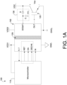
- FIG. 1A is a schematic block diagram of a high-power switching system including a gate driver according to a first possible implementation of the present disclosure.
- the system 100 includes a controller (e.g., microcontroller 110) that controls a switching device 120 via a gate driver 150.
- the gate driver 150 is coupled at an output to a controlling terminal (e.g., gate terminal) of the switching device 120.
- the switching device can be any high-power switching device, including (but not limited to) a power MOSFET or an IGBT.
- the gate driver 150 is configured to provide an output signal (OUT) to change the switch condition (i.e., ON, OFF) of the switching device 120 according to an input signal (IN) from the microcontroller 110.
- the input signal may be a pulse width modulation (PWM) signal that can turn the switching device ON and OFF according to the modulation, such as in a switching power converter.
- the switching device may have a high-side (HS) or a low-side (LS) switch included in a synchronous buck (or boost) converter.
- the gate driver may control a plurality of switching devices, such as in a multiphase (i.e., multichannel) switching power supply. In these implementations it may be necessary to enable/disable the output of the gate driver. For example, in a light load condition a phase including the switching device 120 may be disabled to conserve power. Accordingly, the gate driver may receive an enable signal (EN) from the microcontroller 110 to enable (or disable) its output.
- EN enable signal
- the input signal (IN) to the gate driver 150 may be in a low power domain that spans from a low-power, lower-rail voltage (e.g., low-power ground (GND1) to a low-power, upper-rail voltage (i.e., VDD1), while the output signal (OUT) from the gate driver 150 may be in a high-power domain that spans from a high-power lower rail voltage (e.g., high power ground (GND2) to a high-power, upper-rail voltage (i.e., VDD2).
- a low-power, lower-rail voltage e.g., low-power ground (GND1) to a low-power, upper-rail voltage (i.e., VDD1
- VDD2 high-power, upper-rail voltage
- the gate driver may include electrical isolation 125 between a high-power side and a low-power side.
- the electrical isolation may be implemented with a transformer or capacitor.
- the present disclosure can be applied to gate drivers with, or without, the electrical isolation 125.
- the gate driver 150 may be configured to perform functions that are auxiliary to its primary function of switching.
- the gate driver may be configured with a fault protection function.
- a fault can be an over current condition created by a low impedance (e.g., short circuit) in the switching device.
- the over current condition may be created by a load coupled to the switching device.
- a high current drawn by the load e.g., when the load is shorted
- Fault (i.e., over current) protection can be implemented in a variety of ways.
- FIG 1A illustrates a possible implementation of a gate driver configured to determine over current by a desaturation of the switching device.
- FIG. 2A illustrates a possible implementation of a gate driver configured to determine over current based on a current sensed in a sense resistor coupled to the switching device.
- FIG. 1A illustrates overcurrent protection implemented by sensing desaturation of the switching device 120.
- Sensing desaturation can include measuring a collector-emitter voltage (V CE ) of the switching device (e.g., IGBT) using a detection circuit 130.
- the detection circuit 130 can include a diode (D) so that the measurement of V CE occurs when the switching device 120 is in the ON condition.
- the detection circuit 130 can further include a capacitor (C) that is charged to V CE while the switching device is in the ON condition. A time constant of the capacitor charging may help to filter changes to V CE during normal switching.
- the switching device operates as an ON/OFF switch to conduct/block current to a load when it is in saturation mode.
- the saturation mode may depend on a collector-emitter voltage of the switching device.
- a collector-emitter voltage (V CE ) can be a few volts (e.g., 1 ⁇ V CE ⁇ 4) when the IGBT is in saturation mode.
- V CE collector-emitter voltage
- the current conducted by the IGBT increase thereby increasing the collector-emitter voltage (V CE ) pushing the IGBT out of saturation mode.
- a high collector-emitter voltage (V CE ) may indicate that the IGBT has become desaturated and is conducting a high current.
- the voltage on the capacitor (C) of the detection circuit 130 can be referred to as the desaturation signal (i.e., DESAT).
- DESAT desaturation signal
- the desaturation signal (DESAT) can be compared to a threshold (e.g., 7 ⁇ V DESAT_THR ⁇ 9) and when the threshold is exceeded then the controller may change the state of a fault signal (i.e., FLT) transmitted to the microcontroller 110.
- the microcontroller 110 may change the state of the enable signal (EN) transmitted to the gate driver 150. Switching operation is not resumed until a reset signal (i.e., RST) is received at the gate driver 150.
- the reset signal (RST) may reset the fault signal (FLT) state back to no-fault.
- the reset signal (RST) may further re-engage the detection circuit to monitor the desaturation signal.
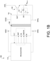
- FIG 1B is a schematic block diagram of a high-power switching system including a gate driver according to a second possible implementation of the present disclosure in which current sensing is used for overcurrent protection.
- a sense resistor (R SHUNT ) is coupled in series (e.g., between an emitter terminal and a ground) with a switching device 120 to sense the current flowing through the switching device as a current sense (CS) signal (i.e., voltage).
- CS current sense
- a filter 131 e.g., low-pass filter
- the microcontroller may transmit a desaturation-check signal (DSCHK) to the gate driver 150.
- the desaturation-check signal can mimic a fault condition in the circuitry of the gate driver so that the gate driver transmits a fault signal (FLT) indicating a fault.
- FLT fault signal
- the microcontroller may transmit a DSCHK signal and monitor the FLT signal to see if the fault monitoring circuitry is working properly.
- the microcontroller may transmit a current-sense-check signal (CSCHK) to the gate driver 151.
- CSCHK current-sense-check signal
- the CS-check signal can mimic a fault condition in the circuitry of the gate driver so that the gate driver transmits a fault signal (FLT) indicating a fault. Accordingly, the microcontroller may transmit a CSCHK signal and monitor the FLT signal to see if the fault monitoring circuitry is working properly.
- FLT fault signal
- the high-power switching systems shown in FIG. 1A and FIG. 1B illustrate the auxiliary signals (FLT, RST, EN, (DSHK or CSCHK)) communicated between the microcontroller 110 and the gate driver 150.
- These signals may be binary signals that are either in a HIGH state (e.g., approximately VDD1) or a LOW state (e.g., approximately GND1) to indicate a condition of the signal.
- a condition may exist for a HIGH signal and may not exist for a LOW signal or vice versa.
- inverse signals may be defined as well.
- a fault-bar signal FLTb
- RSTb reset-bar signal
- the microcontroller 110 may be configured to interpret signals or their inverse counterparts.
- the gate drivers of FIGS 1A , 1B may include a pin (i.e., channel) to communicate each auxiliary signal, but it may be advantageous from a size, cost, and complexity standpoint to minimize the number of pins (i.e., channels) necessary for communicating the auxiliary signals. Accordingly, the present disclosure describes a gate driver configured to effectively combine the reset (RST), enable (EN), and fault check signals (i.e., DSCHK, CSCHK) into a single multifunction signal (MFP). By combining the signals, only one pin (i.e., multi-function pin) is used (e.g., is necessary) for receiving these signals from the microcontroller, thereby reducing the cost and complexity of the gate driver.
- RST reset
- EN enable
- fault check signals i.e., DSCHK, CSCHK
- the present disclosure describes a multifunction signal that is switched between a HIGH level and a LOW level (i.e., modulated) in order to (i) enable/disable the gate driver, (ii) reset a fault condition in the gate driver, and (iii) activate a fault test (i.e., DESAT test, CS test).
- a gate driver that includes circuitry (e.g., logic) configured to interpret the auxiliary signals from the multifunction signal (MFP).
- the gate driver may include circuitry (e.g., logic) to generate a reset signal (RST) from the multifunction signal (MFP).
- the gate driver may include circuitry to generate a desaturation check signal (DSCHK) or current-sense check signal (CSCHK) from the multifunction signal (MFP).
- FIG. 2A is a schematic block diagram of a gate driver according to a first possible implementation of the present disclosure.
- the gate driver includes gate driver circuit 211 coupled to an input pin 210 and configured to receive an input signal (IN).
- the IN signal can be a digital signal with HIGH/LOW levels corresponding to desired ON/OFF switch states.
- the IN signal may be input to a first comparator 212 with hysteresis to remove switching noise.
- the output of the first comparator 212 may be coupled to logic (e.g., AND gate 214).
- the AND gate 214 is further configured to receive a multifunction signal (MFP) from the output of a second comparator 213 with hysteresis.
- the second comparator 213 is configured to receive the multifunction signal from an MFP pin 215 of the gate driver 200.
- MFP multifunction signal
- the AND gate 214 is configured to output a HIGH signal when the IN signal and the MFP signal are HIGH and to output a LOW signal otherwise.
- the MFP signal may function as an enable signal because the input signal (IN) can pass the AND gate 214 when the MFP signal is HIGH and not pass the AND gate 214 when the MFP signal is LOW.
- the output of the AND gate 214 is coupled to an amplifier 216 that is configured to convert the low-power input signal (IN) to a high-power output signal (OUT).
- the output of the amplifier 216 is coupled to an output pin 218 of the gate driver 200, which can be coupled to a controlling terminal of a high-power switching device.
- the gate driver 200 is configured to monitor a desaturation signal (DESAT) at a desaturation pin 220.
- the DESAT signal can be a voltage of an externally coupled capacitor (C), which can indicate if the switching device is in a saturation mode.
- the gate is configured to measure the DESAT signal while the switching device is ON.
- the gate driver includes a DESAT discharge transistor (i.e., discharge transistor 222) that is coupled between the DESAT pin and a ground (e.g., GND2).
- a controlling terminal (e.g., gate terminal) of the discharge transistor 222 is coupled to logic (e.g., NOR gate) that is configured to ground the DESAT pin 220 when the switching device is OFF (i.e., the input signal is LOW).
- the logic may be implemented as a NOR gate 224 that receives the IN signal while the gate driver is enabled and further receives a desaturation check signal (DSCHK).
- the DSCHK signal can be LOW in normal conditions and can be HIGH during a test of the desaturation circuitry.
- the gate driver is (i) disabled or (ii) performing a desaturation test, the state of the discharge transistor corresponds to the input signal. For example, while the IN signal is HIGH (i.e., the switching device is ON), the discharge transistor 222 is OFF, and while the IN signal is LOW (i.e., the switching device is OFF), the discharge transistor 222 is ON.
- the discharge transistor 222 may be coupled to the input of a fault detector circuit (i.e., fault detector 230) and its ON/OFF state may enable/disable operation of the fault detector 230.
- the fault detector 230 When enabled (i.e., discharge transistor 222 is OFF), the fault detector 230 may be configured to receive the DESAT signal and to output a fault signal (FAULT) when the DESAT signal satisfies a criterion.
- the fault detector 230 may compare the DESAT signal (i.e., Vc) to a threshold (V DESAT-THR ) and make the FAULT signal HIGH when the DESAT signal exceeds the threshold, otherwise the FAULT signal is LOW.
- the fault detector 230 may include a comparator 231 with the DESAT signal (Vc) at a non-inverting terminal and a threshold voltage (V DESAT-THR ) at an inverting terminal of the comparator 231.
- the threshold voltage may be generated by a voltage source 232 coupled to the inverting terminal of the comparator 231.
- the fault detector 230 may further include a current source (I DESAT ) that is coupled between an upper rail voltage (e.g., VDD) and the DESAT pin 220.
- the current source (I DESAT ) is configured to charge the capacitor (C), which is coupled externally to the DESAT pin 220 during a DESAT test.
- the capacitor (C) can also be coupled to a collector terminal of an IGBT (not shown) so that the current source will help charge the capacitor (C) to the collector-emitter voltage (V CE ) of the IGBT when it is ON.
- V CE collector-emitter voltage
- the output of the fault detector 230 can be a fault signal (FAULT) that is HIGH when a fault (e.g., high current condition) is detected and is LOW when no fault (e.g., normal current condition) is detected.
- the fault signal (FAULT) is coupled to a fault communication circuit 245 that includes a latch (e.g., SR latch).
- the latch 240 can be configured to hold the FAULT signal HIGH until it is reset by a reset signal (RST).
- RST reset signal
- the output of the latch 240 can be coupled to a fault-bar pin via an output transistor 251.
- the FAULT signal may be latched HIGH by the latch 240 to switch an output transistor 251 ON to couple a fault-bar pin 250 to a ground (e.g., GND).
- a fault-bar signal FLTb is an inverted version of the fault signal (FAULT) that is held LOW by a latch 240 until it is cleared by a reset signal.
- the disclosed gate driver can also be configured in a test mode to perform a DESAT test.
- a DESAT test the DESAT signal is forced to satisfy the fault criterion.
- the FLTb signal can be monitored. If the FLTb signal responds properly to the fault, then the DESAT functionality is verified (i.e., the DESAT test passes).
- a proper response to the fault can be the FLTb signal transitioning to a LOW level, where it is held by the latch. If the FLTb signal does not respond properly to the fault (e.g., the FLTb signal does not transition to a latched LOW state), then the DESAT functionality is not verified (i.e., the DESAT test fails).
- the gate driver 200 includes activation logic 500 (e.g., DSCHK activation logic) that can interpret the MFP signal in the context of other signals, such as the input signal (IN) and the fault signal (FAULT), to configure the gate driver according to multiple functions.
- activation logic 500 e.g., DSCHK activation logic
- the multiple functions can include (i) disabling the output signal, (ii) starting a DESAT test (e.g., to generate a fault condition), and resetting the fault condition (e.g., to resume normal operation).
- the multiple functions may correspond to multiple states (i.e., conditions) of the gate driver.
- the gate driver may be said to be in a disabled condition (i.e., disabled state).
- the gate driver may be said to be in a test condition (i.e., test state).
- a fault is detected, the gate driver may be said to be in a fault condition (i.e., fault state).
- the gate driver may be in a normal condition (i.e., normal state) when it is not in a disabled state, a test state, and a fault state.
- FIG. 2B is a schematic block diagram of a gate driver according to a second possible implementation of the present disclosure.
- the gate driver includes a fault communication circuit 245 and a gate driver circuit 211 as in FIG. 2A , but includes a fault detector circuit (i.e., fault detector 270) based on a sensed current signal (CS) rather than a DESAT signal.
- a fault detector circuit i.e., fault detector 270
- CS sensed current signal
- DESAT DESAT signal
- the output of the fault detector 270 can be a fault signal (FAULT) that is high when a fault (e.g., high current condition is detected and LOW when no fault (e.g., normal current condition) is detected.
- FAULT fault signal
- a current sense pin 221 is coupled by a first switch 274 to a positive input of a comparator 231, while an upper supply voltage (VDD) is decoupled by a second switch 273 from the positive input of the comparator 231.
- the comparator 231 is configured to compare the voltage (i.e., the CS signal) to a current-sense threshold (V CS-THR ) coupled to a negative terminal of the comparator. When the CS signal exceeds the current-sense threshold (V CS-THR ), the fault detector 270 is configured to trigger the fault state in the gate driver.
- the gate driver further includes activation logic 500 (i.e., CSCHK activation logic) that is configured to interpret MFP signals in the context of other signals, such as the input signal (IN) and the fault signal (FAULT), to configure the gate driver according to multiple functions.
- activation logic 500 i.e., CSCHK activation logic
- the multiple functions can include (i) disabling the output signal, (ii) starting a CS test (e.g., to generate a fault condition), and resetting the fault condition (e.g., to resume normal operation).
- the activation logic 500 is further configured to deactivate the CS test (i.e., reset the fault condition) after the test has concluded by coupling the CS pin to the positive input of the comparator 231 via the first switch 274 and decoupling the upper rail voltage (VDD) from the positive input of the comparator 231 via the second switch 273.
- An inverter 275 can be included so that the switches may be controlled in complementary fashion.
- FIG. 3 are graphs of signals illustrating functions controlled by a multifunction signal (MFP) according to a possible implementation of the present disclosure.
- MFP multifunction signal
- the signals are aligned in time and alternate between HIGH levels and LOW levels to indicate conditions and alter operation of the gate driver.
- the graphs include a DSCHK signal, but it should be understood that a CSCHK signal could behave similarly.
- the gate driver is in normal operation (i.e., in a normal state).
- the MFP signal is HIGH to enable the output so that the OUT signal follows (i.e., matches) the IN signal.
- the FLTb signal is HIGH indicating that no fault (i.e., high current) is detected and the DSCHK signal is LOW indicating that a DESAT test is not underway.
- the output of the gate driver is disabled (i.e., the gate driver is in a disabled state).
- the MFP signal is LOW to disable the output.
- the OUT signal is LOW despite HIGH levels of IN signal.
- the output was disabled for a reason other than a fault or a DESAT test because during the second period, the FLTb signal is HIGH indicating that no fault condition and the DSCHK signal is LOW indicating that a DESAT test is not underway.
- the normal operation i.e., the normal state
- the MFP signal is HIGH to enable the output so that the OUT signal again follows (i.e., matches) the IN signal.
- the FLTb signal is HIGH indicating that no fault (i.e., high current) is detected and the DSCHK signal is LOW indicating that a DESAT test is not underway.
- the FLTb signal transitions LOW indicating that a fault is detected.
- the LOW FLTb signal disables the output.
- the gate driver is disabled, and the gate driver is in fault operation (i.e., in a fault state).
- the output is disabled by the FLTb signal being LOW despite the MFP signal being HIGH.
- the HIGH output signal (OUT) may be turned off slowly when being disabled to prevent voltage spikes (e.g., due to back EMF).
- the output may be disabled according to a soft turn off 337 (i.e., STO).
- the amplifier 216 of the gate driver 200 shown in FIGS. 2A-2B can be configured to reduce the OUT signal according to a soft turn off (i.e., soft shutdown) profile.
- the MFP signal is transitioned LOW so that both the FLTb and the MFP signal are LOW. If this condition is held for more than a minimum reset period (T RST_MIN ) then the FLTb signal is reset to a HIGH level indicating no fault condition. Additionally, the MFP signal can be reset to a HIGH level to enable the output so that a normal condition is restored during a fifth period 350.
- T RST_MIN a minimum reset period
- the input signal (IN) may be turned off and the MFP signal may be pulsed (i.e., toggled) for a number of consecutive pulses to begin a DESAT test.
- the gate driver is in a DESAT test operation (i.e., DESAT test state) a DSCHK signal is transition HIGH to disable the discharge transistor 222 so that the external capacitor (C) can be charged for the test.
- FIG. 4 illustrates a state diagram that summarizes the states and the transitions between states, such as described with the signals of FIG. 3 .
- the gate driver can operate in a normal state 410 (i.e., normal mode) in which the output signal follows the input signal.
- the normal state 410 may be the most common operating state of the gate driver. Operation in states other than the normal state may be temporary and may ultimately result in a return to the normal state.
- the gate driver can also operate in a disabled state 420 (i.e., disabled mode) in which the output is held LOW.
- the gate driver may transition from the normal state 410 to the disabled state 420 and from the disabled state 420 to the normal state 410 according to a level of the MFP signal.
- the gate driver can operate in a disabled state even when there is no fault detected.
- the gate driver can also operate in a fault state 430 (i.e., fault mode) in which the output is held LOW.
- the gate driver may transition from the normal state 410 to the fault state 430 according to a level of the FTLb signal. In the fault mode, the FLTb signal is latched at a LOW level.
- the gate driver may transition from the fault state 430 to the normal state 410 when the MFP signal is held LOW for a period greater than or equal to a threshold (T RST-MIN ).
- the gate driver can also operate in a DESAT test state 440 (i.e., DESAT test mode, DSCHK mode) in which the DSCHK signal is held HIGH.
- the gate driver may transition from the normal state 410 to the DESAT test state 440 after the MFP signal is pulsed (e.g., HIGH/LOW/HIGH) for a number of times (e.g., 15 times).
- the voltage at the DESAT pin can be charged until it exceeds a threshold (V DESAT-THR ), thereby changing the FLTb level.
- the gate driver may transition from the DESAT test state 440 to the fault state 430 according to the FLTb level.
- the gate driver may transition from the fault state 430 to the normal state 410 when the MFP signal is held LOW for a period greater than or equal to a threshold (T RST-MIN ).
- the gate driver 200 further includes activation logic 500 to generate the DSCHK signal or CSCHK signal (i.e., DSCHK/CSCHK singal).
- FIG. 5 is a schematic block diagram of an activation logic circuit according to a possible implementation of the present disclosure.
- the activation logic 500 is configured to control a level of a desaturation check signal (DSCHK) or a current sense check signal (CSCHK).
- DSCHK desaturation check signal
- CSCHK current sense check signal
- the activation logic is configured to make the DSCHK/CSCHK signal HIGH when the MFP signal is pulsed (i.e., toggled) for a number of cycles.
- a HIGH DSCHK/CSCHK signal can configure the gate driver in a DESAT test state to charge the external capacitor (C) or a CS test state to couple the upper rail voltage to the input of the comparator.
- the activation logic 500 includes a shift register 510.
- the input of the shift register 510 can be coupled to a HIGH signal (i.e., VDD) and the output of the shift register is the DSCHK/CSCHK signal.
- the shift register includes a plurality of flip-flops (e.g., D-type flip-flops) coupled in series.
- the MFP signal may be coupled to a clock input of each of the flip flops so as the MFP signal is pulsed, the HIGH signal shifts to the output of the shift register. For example, if four flip flops are implemented then the MFP signal can be pulsed four times for the HIGH signal (VDD) to reach the output.
- the activation logic may include a low pass filter 520 coupled between the MFP signal and the shift register 510. The low pass filter 520 may remove spurious signals from the MFP signal that could cause shift errors in the shift register 510.
- the DSCHK/CSCHK signal may be deactivated (i.e., made LOW) by clearing the shift register 510.
- the shift registered may be cleared in several conditions.
- the activation logic includes a logic gate (e.g., NOR gate 533) configured to clear the flip-flops of the shift register.
- the NOR gate 533 is configured to receive a reset signal (RST), the input signal (IN), and the fault signal (FAULT).
- the NOR gate is configured to clear the shift register 510 if the RST signal is LOW, the IN signal is HIGH, or the FAULT signal is HIGH.
- the DSHK signal may be deactivated (i.e., the DESAT test ended) by holding the MFP signal LOW for a period that is greater than a threshold (e.g., T RST-MIN ).
- the gate driver 200 includes a low pass filter 260 that is configured to receive the MFP signal and output the RST signal. A delay associated with the low pass filter 260 may help to create the threshold (T RST-MIN ) that is satisfied for the RST to change states and clear the shift register 510.
- FIG. 6 illustrates terminating a DSCHK mode (i.e., DESAT test state) by holding the MFP signal low for a period (T RST-MIN ). While shown for the DSCHK mode, it may be understood that a CSCHK mode could operate similarly.
- the DSCHK signal is transitioned HIGH as a result of the MFP signal pulsing for a number of pulses determined by the shift register (e.g., 15 pulses).
- the gate driver enters the DSCHK mode, and the external capacitor is charged, thereby raising the DESAT signal.
- the DESAT signal is allowed to rise above a threshold (e.g., V DESAT-THR )
- a threshold e.g., V DESAT-THR
- the MFP signal is held low for a period (T RST-MIN ) before a fault occurs.
- the shift register is cleared so that the DSCHK signal is transitioned LOW and the gate driver returns to the NORMAL state.
- the charge on the capacitor i.e., DESAT signal
- the discharge transistor 222 is low, as is the case shown here.
- FIG. 7 illustrates a DSCHK mode (i.e., DESAT test state) that is prevented when the IN signal is HIGH. While shown for the DSCHK mode, it may be understood that a CSCHK mode could operate similarly.
- the MFP signal is toggled to begin a DESAT test (i.e., make DSCHK HIGH).
- the IN signal is transition HIGH. This clears the shift register and as a result DSCHK is held LOW.
- the HIGH IN signal prevents the gate driver from entering the DESAT test state and remains in NORMAL mode.
- the OUT signal follows the IN signal but is disabled when the MFP signal is pulsed LOW.
- the gate driver When the OUT signal is held HIGH by the IN signal the DESAT signal charges and eventually at a third time 730, a fault condition is reached, making the FAULT signal HIGH.
- the gate driver enters the FAULT state.
- the output is shut down (e.g., according to a soft turn off (STO) profile 735.
- the FAULT signal may trigger the amplifier 216 to perform a soft shutdown (SSD) of its output (see FIG. 2 ).
- the gate driver remains in the fault state (i.e., FLTb is LOW) until it is returned to a NORMAL state at a fourth time 740 by holding the MFP signal LOW for a period.
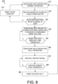
- FIG. 8 is a method for controlling a gate driver to test its Wash detector circuit.
- the method 800 includes configuring 810 the gate driver for normal operation (i.e., OUT signal at OUT pin follows IN signal at IN pin).
- the method 800 further includes receiving 820 a series of pulses at a multifunction pin of the gate driver.
- the gate driver can receive the pulses until a first criterion 830 is satisfied.
- the first criterion may be receiving a number of consecutive pulses while the IN signal is LOW. If the first criterion is not satisfied, then the gate driver may be configured to reset 815 a pulse counter (e.g., shift register) and return to normal operation 810.
- a pulse counter e.g., shift register
- the method 800 further includes configuring 840 the gate driver to charge an external capacitor, which generates an increasing DESAT voltage.
- the DESAT voltage can continue to increase until it satisfies a second criterion 850.
- the second criterion 850 may be the DESAT voltage exceeding a threshold.
- the method 800 further includes configuring 860 the gate driver for fault operation (i.e., FAULT state).
- the gate driver may be configured to discharge the external capacitor and transmit a fault signal (FLTb) to a fault pin of the gate driver.
- the fault operation can continue until an MFP signal is received 870 that satisfies a third criterion 880.
- the third criterion 880 can be that the MFP signal at the multifunction pin is held LOW for a period longer than a threshold time.
- the method 800 includes clearing 890 the fault and returning the gate driver to normal operation 810 (i.e., NORMAL state).
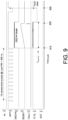
- FIG. 9 illustrates signals of the gate driver during a test of its fault sensing capabilities, such as described for the method illustrated in FIG. 8 . While shown for the DSCHK mode, it may be understood that a CSCHK mode could operate similarly.
- a series of 15 consecutive pulses in the MFP signal is received at the gate driver while the IN signal is LOW, thus satisfying the first criterion of the method described above.
- the gate driver is configured to charge an external capacitor, which increases a DESAT signal.
- the DESAT signal exceeds a threshold, thus satisfying the second criterion of the method described above.
- the gate driver is configured to generate a fault (FAULT) which clears the DESAT signal and latches a fault signal (FLTb) at a fault pin of the gate driver LOW.
- FULT fault
- FLTb fault signal
- the MFP signal is held LOW for a period, thus satisfying the third criterion of the method described above.
- the gate driver is configured to reset the fault signal (FLTb), which ends the test.
- Some implementations may be implemented using various semiconductor processing and/or packaging techniques. Some implementations may be implemented using various types of semiconductor processing techniques associated with semiconductor substrates including, but not limited to, for example, Silicon (Si), Gallium Arsenide (GaAs), Gallium Nitride (GaN), Silicon Carbide (SiC) and/or so forth.
- semiconductor substrates including, but not limited to, for example, Silicon (Si), Gallium Arsenide (GaAs), Gallium Nitride (GaN), Silicon Carbide (SiC) and/or so forth.
- a singular form may, unless definitely indicating a particular case in terms of the context, include a plural form.
- Spatially relative terms e.g., over, above, upper, under, beneath, below, lower, and so forth
- the relative terms above and below can, respectively, include vertically above and vertically below.
- the term adjacent can include laterally adjacent to or horizontally adjacent to.
Landscapes
- Power Conversion In General (AREA)
Abstract
Description
- This application claims priority to
U.S. Application No. 17/653,730 filed on March 7, 2022 U.S. Provisional Application No. 63/262,264, filed on October 8,2021 - The present disclosure relates to power integrated circuits and more specifically to a gate driver configured to switch and monitor a high-power switching device.
- A gate driver is an integrated circuit configured to convert a low power switching signal, such as from a microcontroller, into a high current signal suitable for driving a high-power switching device, such as a power metal oxide semiconductor field effect transistor (MOSFET) or an insulated gate bipolar transistor (IGBT). In other words, the gate driver can be an interface between a low-power domain and a high-power domain and may include electrical isolation to separate the power domains. It is often necessary to monitor the condition of the high-power switching device for safety and reliability. For example, an overcurrent condition can cause damage to the switching device and/or to its coupled devices (e.g., capacitors). Further, the over current condition could result in a safety concern to a user because of the high-power levels of an over current. Accordingly, the gate driver may be further configured to sense conditions of the high-power switching device and report these conditions to the microcontroller. As a result, the gate driver may be configured to communicate with the microcontroller.
- In another aspect, the present disclosure generally describes a high-power switching system that includes a switching device, a gate driver, and a controller. The controller is configured to transmit an input signal to an input pin (IN) of the gate driver to control operation of the switching device. The controller is further configured to receive a fault signal at a fault pin (FLTb) of the gate driver to monitor a fault in the switching device. The controller is further configured to transmit a multifunction signal to a multifunction pin (MFP) of the gate driver to control operation of the gate driver. The gate driver is configured by the multifunction signal to disable an output of the gate driver, activate a fault test to test a fault detector circuit of the gate driver and clear a fault detected by the fault detector circuit of the gate driver.
- In at least one aspect, the present disclosure generally describes a gate driver that includes a driver circuit, a fault detector circuit, a fault communication circuit, and a multifunction pin (MFP). The driver circuit is configured to receive an input signal at an input pin (IN) of the gate driver and to transmit an output signal to a switching device coupled at a gate terminal to an output pin (OUT) of the gate driver. The fault detector circuit is configured to receive a desaturation signal at a desaturation pin (DESAT) of the gate driver (or to receive a current sense signal at a current-sense (CS) pin of the gate driver) in order to detect a fault in the switching device. The fault communication circuit is coupled to the fault detector circuit and is configured to (i) set a fault signal when a fault is detected and (ii) transmit the fault signal to a fault pin (FLTb) of the gate driver. The multifunction pin (MFP) of the gate driver is configured to receive a multifunction signal, which can configure the gate driver to (i) enable/disable the driver circuit, (ii) activate a test of the fault detector circuit, and (iii) reset the fault communication circuit.
- In a possible implementation of the gate driver, the driver circuit is configured to transmit a LOW output signal when the multifunction signal is LOW.
- In another possible implementation of the gate driver, the driver circuit is (i) configured to transmit a LOW output signal when the multifunction signals is LOW and (ii) configured to transmit an output signal that is a replica of the input signal when the multifunction signal is HIGH.
- In another possible implementation of the gate driver, the fault communication circuit includes a latch that is set to a fault level by the fault detector circuit in response to a fault.
- In another possible implementation of the gate driver, the fault communication circuit includes a latch that is set to a fault level by the fault detector circuit in response to a fault and the latch is reset to a normal level by a multifunction signal that is held LOW for a period that is at least as long as a threshold period.
- In another possible implementation of the gate driver, the fault detector circuit includes a shift register that is coupled to the multifunction pin. The shift register is configured to output a DSCHK signal to activate the test of the fault detector circuit after receiving a number of consecutive pulses in the multifunction signal.
- In another possible implementation of the gate driver, the fault detector circuit includes a capacitor that is coupled externally to the gate driver at the DESAT pin; a discharge transistor configured to discharge the capacitor to ground when turned ON; and a current source configured to charge the capacitor when the discharge transistor is turned OFF. The voltage on the capacitor is the desaturation signal at the DESAT pin.
- In another possible implementation of the gate driver, the fault detector circuit includes a capacitor that is coupled externally to the gate driver at the DESAT pin; a discharge transistor configured to discharge the capacitor to ground when turned ON; and a current source configured to charge the capacitor when the discharge transistor is turned OFF. The voltage on the capacitor is the desaturation signal at the DESAT pin, and the discharge transistor is turned OFF to activate the test of the fault detector circuit. The test of the fault detector circuits includes charging the capacitor to increase the voltage at the DESAT pin, comparing the voltage at the DESAT pin to a threshold, and detecting a fault when the voltage exceeds the threshold.
- In another aspect, the present disclosure generally describes a method for testing a fault detector circuit of a gate driver. The method includes (i) receiving a multifunction signal at a multifunction pin of the gate driver, (ii) detecting pulses in the multifunction signal, and (iii) determining that the pulses satisfy a first criterion. Upon satisfying the first criterion the method includes configuring the gate driver to charge an external capacitor, which increases a DESAT signal received at a DESAT pin of the gate driver. Then the method further includes determining that the DESAT signal satisfies a second criterion and holding a fault signal on a fault pin of the gate driver. The method further includes (i) detecting a level change in the multifunction signal, (ii) determining that the level change satisfies a third criterion and (iii) resetting the fault signal on the fault pin.
- The foregoing illustrative summary, as well as other exemplary objectives and/or advantages of the disclosure, and the manner in which the same are accomplished, are further explained within the following detailed description and its accompanying drawings.
-
-
FIG. 1A is a schematic block diagram of a high-power switching system including a gate driver according to a first possible implementation of the present disclosure. -
FIG 1B is a schematic block diagram of a high-power switching system including a gate driver according to a second possible implementation of the present disclosure. -
FIG. 2A is a schematic block diagram of a gate driver according to a first possible implementation of the present disclosure. -
FIG. 2B is a schematic block diagram of a gate driver according to a second possible implementation of the present disclosure. -
FIG. 3 are graphs of signals illustrating functions controlled by a multifunction signal according to a possible implementation of the present disclosure. -
FIG. 4 illustrates a state diagram that summarizes the states of the gate driver and the transitions between states. -
FIG. 5 is a schematic block diagram of a desaturation check (DSCHK) activation logic according to a possible implementation of the present disclosure. -
FIG. 6 are graphs of signals illustrating terminating a DESAT test according to a possible implementation of the present disclosure. -
FIG. 7 are graphs of signals illustrating preventing a DESAT test and responding to a fault according to a possible implementation of the present disclosure. -
FIG. 8 is a method for controlling a gate driver to perform a test of its fault sensing capabilities according to a possible implementation of the present disclosure. -
FIG. 9 are graphs of signals illustrating a gate driver performing a test of its fault sensing capabilities according to a possible implementation of the present disclosure. - The components in the drawings are not necessarily to scale relative to each other. Like reference numerals designate corresponding parts throughout the several views.
- The present disclosure describes a gate driver that includes circuitry and protocols necessary for communicating with a microcontroller (i.e., controller) regarding functions other than switching (i.e., auxiliary functions). These auxiliary functions can include functions related to sensing and responding to a fault condition and may include (i) disabling an output of the driver (e.g., in response to a sensed fault condition), (ii) resetting a state of a fault detector (e.g., after a fault condition has ended), and (iii) testing a fault detector (e.g., to ensure it is operable). The disclosed circuits and methods may advantageously simplify the complexity of the communication with the microcontroller by combining these functions at a single input/output pin of the gate driver. In other words, the disclosed gate driver includes a multi-function pin.
-
FIG. 1A is a schematic block diagram of a high-power switching system including a gate driver according to a first possible implementation of the present disclosure. Thesystem 100 includes a controller (e.g., microcontroller 110) that controls aswitching device 120 via agate driver 150. Thegate driver 150 is coupled at an output to a controlling terminal (e.g., gate terminal) of theswitching device 120. The switching device can be any high-power switching device, including (but not limited to) a power MOSFET or an IGBT. Thegate driver 150 is configured to provide an output signal (OUT) to change the switch condition (i.e., ON, OFF) of theswitching device 120 according to an input signal (IN) from themicrocontroller 110. For example, the input signal may be a pulse width modulation (PWM) signal that can turn the switching device ON and OFF according to the modulation, such as in a switching power converter. For example, the switching device may have a high-side (HS) or a low-side (LS) switch included in a synchronous buck (or boost) converter. Further, the gate driver may control a plurality of switching devices, such as in a multiphase (i.e., multichannel) switching power supply. In these implementations it may be necessary to enable/disable the output of the gate driver. For example, in a light load condition a phase including theswitching device 120 may be disabled to conserve power. Accordingly, the gate driver may receive an enable signal (EN) from themicrocontroller 110 to enable (or disable) its output. - The input signal (IN) to the
gate driver 150 may be in a low power domain that spans from a low-power, lower-rail voltage (e.g., low-power ground (GND1) to a low-power, upper-rail voltage (i.e., VDD1), while the output signal (OUT) from thegate driver 150 may be in a high-power domain that spans from a high-power lower rail voltage (e.g., high power ground (GND2) to a high-power, upper-rail voltage (i.e., VDD2). - In some implementations, crosstalk from the high-power domain to the low-power domains can impair function or cause damage to the low power circuitry. According, for these implementations the gate driver may include
electrical isolation 125 between a high-power side and a low-power side. The electrical isolation may be implemented with a transformer or capacitor. The present disclosure can be applied to gate drivers with, or without, theelectrical isolation 125. - As mentioned, the
gate driver 150 may be configured to perform functions that are auxiliary to its primary function of switching. For example, the gate driver may be configured with a fault protection function. A fault can be an over current condition created by a low impedance (e.g., short circuit) in the switching device. Alternatively, the over current condition may be created by a load coupled to the switching device. For example, a high current drawn by the load (e.g., when the load is shorted) may create the over current condition. Fault (i.e., over current) protection can be implemented in a variety of ways.FIG 1A illustrates a possible implementation of a gate driver configured to determine over current by a desaturation of the switching device.FIG. 2A illustrates a possible implementation of a gate driver configured to determine over current based on a current sensed in a sense resistor coupled to the switching device. -
FIG. 1A illustrates overcurrent protection implemented by sensing desaturation of theswitching device 120. Sensing desaturation can include measuring a collector-emitter voltage (VCE) of the switching device (e.g., IGBT) using adetection circuit 130. Thedetection circuit 130 can include a diode (D) so that the measurement of VCE occurs when theswitching device 120 is in the ON condition. Thedetection circuit 130 can further include a capacitor (C) that is charged to VCE while the switching device is in the ON condition. A time constant of the capacitor charging may help to filter changes to VCE during normal switching. - The switching device operates as an ON/OFF switch to conduct/block current to a load when it is in saturation mode. The saturation mode may depend on a collector-emitter voltage of the switching device. For example, a collector-emitter voltage (VCE) can be a few volts (e.g., 1≤ VCE ≤ 4) when the IGBT is in saturation mode. When the load is short-circuited, the current conducted by the IGBT increase thereby increasing the collector-emitter voltage (VCE) pushing the IGBT out of saturation mode. In other words, a high collector-emitter voltage (VCE) may indicate that the IGBT has become desaturated and is conducting a high current. The voltage on the capacitor (C) of the
detection circuit 130 can be referred to as the desaturation signal (i.e., DESAT). The desaturation signal (DESAT) can be compared to a threshold (e.g., 7 ≤ VDESAT_THR ≤ 9) and when the threshold is exceeded then the controller may change the state of a fault signal (i.e., FLT) transmitted to themicrocontroller 110. In response, themicrocontroller 110 may change the state of the enable signal (EN) transmitted to thegate driver 150. Switching operation is not resumed until a reset signal (i.e., RST) is received at thegate driver 150. The reset signal (RST) may reset the fault signal (FLT) state back to no-fault. The reset signal (RST) may further re-engage the detection circuit to monitor the desaturation signal. -
FIG 1B is a schematic block diagram of a high-power switching system including a gate driver according to a second possible implementation of the present disclosure in which current sensing is used for overcurrent protection. In this implementation, a sense resistor (RSHUNT) is coupled in series (e.g., between an emitter terminal and a ground) with aswitching device 120 to sense the current flowing through the switching device as a current sense (CS) signal (i.e., voltage). In a possible implementation a filter 131 (e.g., low-pass filter) is coupled between the sense resistor (RSHUNT) and thegate driver 151. - Some applications (e.g., automotive) require checking the capability of the gate driver's over current protection (i.e., fault monitoring) periodically. For the implementation shown in
FIG. 1A , the microcontroller may transmit a desaturation-check signal (DSCHK) to thegate driver 150. The desaturation-check signal can mimic a fault condition in the circuitry of the gate driver so that the gate driver transmits a fault signal (FLT) indicating a fault. Accordingly, the microcontroller may transmit a DSCHK signal and monitor the FLT signal to see if the fault monitoring circuitry is working properly. For the implementation shown in FIG. IB, the microcontroller may transmit a current-sense-check signal (CSCHK) to thegate driver 151. The CS-check signal can mimic a fault condition in the circuitry of the gate driver so that the gate driver transmits a fault signal (FLT) indicating a fault. Accordingly, the microcontroller may transmit a CSCHK signal and monitor the FLT signal to see if the fault monitoring circuitry is working properly. - The high-power switching systems shown in
FIG. 1A andFIG. 1B illustrate the auxiliary signals (FLT, RST, EN, (DSHK or CSCHK)) communicated between themicrocontroller 110 and thegate driver 150. These signals may be binary signals that are either in a HIGH state (e.g., approximately VDD1) or a LOW state (e.g., approximately GND1) to indicate a condition of the signal. A condition may exist for a HIGH signal and may not exist for a LOW signal or vice versa. Accordingly, inverse signals may be defined as well. For example, a fault-bar signal (FLTb) may be the logical inverse of the FLT signal, and a reset-bar signal (RSTb) may be the logical inverse of the RST signal. Themicrocontroller 110 may be configured to interpret signals or their inverse counterparts. - The gate drivers of
FIGS 1A ,1B may include a pin (i.e., channel) to communicate each auxiliary signal, but it may be advantageous from a size, cost, and complexity standpoint to minimize the number of pins (i.e., channels) necessary for communicating the auxiliary signals. Accordingly, the present disclosure describes a gate driver configured to effectively combine the reset (RST), enable (EN), and fault check signals (i.e., DSCHK, CSCHK) into a single multifunction signal (MFP). By combining the signals, only one pin (i.e., multi-function pin) is used (e.g., is necessary) for receiving these signals from the microcontroller, thereby reducing the cost and complexity of the gate driver. - The present disclosure describes a multifunction signal that is switched between a HIGH level and a LOW level (i.e., modulated) in order to (i) enable/disable the gate driver, (ii) reset a fault condition in the gate driver, and (iii) activate a fault test (i.e., DESAT test, CS test). Accordingly, the present disclosure further describes a gate driver that includes circuitry (e.g., logic) configured to interpret the auxiliary signals from the multifunction signal (MFP). For example, the gate driver may include circuitry (e.g., logic) to generate a reset signal (RST) from the multifunction signal (MFP). Further, the gate driver may include circuitry to generate a desaturation check signal (DSCHK) or current-sense check signal (CSCHK) from the multifunction signal (MFP).
-
FIG. 2A is a schematic block diagram of a gate driver according to a first possible implementation of the present disclosure. The gate driver includesgate driver circuit 211 coupled to aninput pin 210 and configured to receive an input signal (IN). The IN signal can be a digital signal with HIGH/LOW levels corresponding to desired ON/OFF switch states. The IN signal may be input to afirst comparator 212 with hysteresis to remove switching noise. The output of thefirst comparator 212 may be coupled to logic (e.g., AND gate 214). The ANDgate 214 is further configured to receive a multifunction signal (MFP) from the output of asecond comparator 213 with hysteresis. Thesecond comparator 213 is configured to receive the multifunction signal from anMFP pin 215 of thegate driver 200. - The AND
gate 214 is configured to output a HIGH signal when the IN signal and the MFP signal are HIGH and to output a LOW signal otherwise. In other words, the MFP signal may function as an enable signal because the input signal (IN) can pass the ANDgate 214 when the MFP signal is HIGH and not pass the ANDgate 214 when the MFP signal is LOW. The output of the ANDgate 214 is coupled to anamplifier 216 that is configured to convert the low-power input signal (IN) to a high-power output signal (OUT). The output of theamplifier 216 is coupled to anoutput pin 218 of thegate driver 200, which can be coupled to a controlling terminal of a high-power switching device. - The
gate driver 200 is configured to monitor a desaturation signal (DESAT) at adesaturation pin 220. As discussed, the DESAT signal can be a voltage of an externally coupled capacitor (C), which can indicate if the switching device is in a saturation mode. The gate is configured to measure the DESAT signal while the switching device is ON. Accordingly, the gate driver includes a DESAT discharge transistor (i.e., discharge transistor 222) that is coupled between the DESAT pin and a ground (e.g., GND2). A controlling terminal (e.g., gate terminal) of thedischarge transistor 222 is coupled to logic (e.g., NOR gate) that is configured to ground theDESAT pin 220 when the switching device is OFF (i.e., the input signal is LOW). As shown, the logic may be implemented as a NORgate 224 that receives the IN signal while the gate driver is enabled and further receives a desaturation check signal (DSCHK). The DSCHK signal can be LOW in normal conditions and can be HIGH during a test of the desaturation circuitry. In other words, unless the gate driver is (i) disabled or (ii) performing a desaturation test, the state of the discharge transistor corresponds to the input signal. For example, while the IN signal is HIGH (i.e., the switching device is ON), thedischarge transistor 222 is OFF, and while the IN signal is LOW (i.e., the switching device is OFF), thedischarge transistor 222 is ON. - The
discharge transistor 222 may be coupled to the input of a fault detector circuit (i.e., fault detector 230) and its ON/OFF state may enable/disable operation of thefault detector 230. When enabled (i.e.,discharge transistor 222 is OFF), thefault detector 230 may be configured to receive the DESAT signal and to output a fault signal (FAULT) when the DESAT signal satisfies a criterion. For example, thefault detector 230 may compare the DESAT signal (i.e., Vc) to a threshold (VDESAT-THR) and make the FAULT signal HIGH when the DESAT signal exceeds the threshold, otherwise the FAULT signal is LOW. Accordingly, thefault detector 230 may include acomparator 231 with the DESAT signal (Vc) at a non-inverting terminal and a threshold voltage (VDESAT-THR) at an inverting terminal of thecomparator 231. The threshold voltage may be generated by avoltage source 232 coupled to the inverting terminal of thecomparator 231. - The
fault detector 230 may further include a current source (IDESAT) that is coupled between an upper rail voltage (e.g., VDD) and theDESAT pin 220. The current source (IDESAT) is configured to charge the capacitor (C), which is coupled externally to theDESAT pin 220 during a DESAT test. The capacitor (C) can also be coupled to a collector terminal of an IGBT (not shown) so that the current source will help charge the capacitor (C) to the collector-emitter voltage (VCE) of the IGBT when it is ON. When the DESAT test is over and the IGBT is OFF, charge on the capacitor (C) (i.e., voltage (Vc)) may be drained (i.e., decreased) by thedischarge transistor 222. - The output of the
fault detector 230 can be a fault signal (FAULT) that is HIGH when a fault (e.g., high current condition) is detected and is LOW when no fault (e.g., normal current condition) is detected. The fault signal (FAULT) is coupled to afault communication circuit 245 that includes a latch (e.g., SR latch). Thelatch 240 can be configured to hold the FAULT signal HIGH until it is reset by a reset signal (RST). The output of thelatch 240 can be coupled to a fault-bar pin via anoutput transistor 251. - When a fault is detected, the FAULT signal may be latched HIGH by the
latch 240 to switch anoutput transistor 251 ON to couple a fault-bar pin 250 to a ground (e.g., GND). When thelatch 240 is reset to LOW, theoutput transistor 251 is switched OFF and the fault-bar pin 250 is pulled up to an upper rail voltage (e.g., VDD1) by a pull-upresistor 252. Accordingly, a fault-bar signal (FLTb) is an inverted version of the fault signal (FAULT) that is held LOW by alatch 240 until it is cleared by a reset signal. - While the gate driver is configured to provide continuous DESAT protection, the disclosed gate driver can also be configured in a test mode to perform a DESAT test. In a DESAT test, the DESAT signal is forced to satisfy the fault criterion. At the same time the FLTb signal can be monitored. If the FLTb signal responds properly to the fault, then the DESAT functionality is verified (i.e., the DESAT test passes). For example, a proper response to the fault, can be the FLTb signal transitioning to a LOW level, where it is held by the latch. If the FLTb signal does not respond properly to the fault (e.g., the FLTb signal does not transition to a latched LOW state), then the DESAT functionality is not verified (i.e., the DESAT test fails).
- The
gate driver 200 includes activation logic 500 (e.g., DSCHK activation logic) that can interpret the MFP signal in the context of other signals, such as the input signal (IN) and the fault signal (FAULT), to configure the gate driver according to multiple functions. The multiple functions can include (i) disabling the output signal, (ii) starting a DESAT test (e.g., to generate a fault condition), and resetting the fault condition (e.g., to resume normal operation). - The multiple functions may correspond to multiple states (i.e., conditions) of the gate driver. For example, while the output is disabled, the gate driver may be said to be in a disabled condition (i.e., disabled state). While a DESAT test is being performed, the gate driver may be said to be in a test condition (i.e., test state). While a fault is detected, the gate driver may be said to be in a fault condition (i.e., fault state). The gate driver may be in a normal condition (i.e., normal state) when it is not in a disabled state, a test state, and a fault state.
-
FIG. 2B is a schematic block diagram of a gate driver according to a second possible implementation of the present disclosure. The gate driver includes afault communication circuit 245 and agate driver circuit 211 as inFIG. 2A , but includes a fault detector circuit (i.e., fault detector 270) based on a sensed current signal (CS) rather than a DESAT signal. As before the output of thefault detector 270 can be a fault signal (FAULT) that is high when a fault (e.g., high current condition is detected and LOW when no fault (e.g., normal current condition) is detected. In a normal mode, acurrent sense pin 221 is coupled by afirst switch 274 to a positive input of acomparator 231, while an upper supply voltage (VDD) is decoupled by asecond switch 273 from the positive input of thecomparator 231. Thecomparator 231 is configured to compare the voltage (i.e., the CS signal) to a current-sense threshold (VCS-THR) coupled to a negative terminal of the comparator. When the CS signal exceeds the current-sense threshold (VCS-THR), thefault detector 270 is configured to trigger the fault state in the gate driver. - The gate driver further includes activation logic 500 (i.e., CSCHK activation logic) that is configured to interpret MFP signals in the context of other signals, such as the input signal (IN) and the fault signal (FAULT), to configure the gate driver according to multiple functions. The multiple functions can include (i) disabling the output signal, (ii) starting a CS test (e.g., to generate a fault condition), and resetting the fault condition (e.g., to resume normal operation).
- In a CS test the fault logic may configure the
first switch 274 to decouple theCS pin 221 from the positive input of thecomparator 231 and thesecond switch 273 to couple the upper rail voltage (VDD) to the positive input of thecomparator 231 in order to trigger a fault condition (i.e., FAULT = HIGH). Theactivation logic 500 is further configured to deactivate the CS test (i.e., reset the fault condition) after the test has concluded by coupling the CS pin to the positive input of thecomparator 231 via thefirst switch 274 and decoupling the upper rail voltage (VDD) from the positive input of thecomparator 231 via thesecond switch 273. Aninverter 275 can be included so that the switches may be controlled in complementary fashion. -
FIG. 3 are graphs of signals illustrating functions controlled by a multifunction signal (MFP) according to a possible implementation of the present disclosure. In thegraphs 300, the signals are aligned in time and alternate between HIGH levels and LOW levels to indicate conditions and alter operation of the gate driver. The graphs include a DSCHK signal, but it should be understood that a CSCHK signal could behave similarly. - During a
first period 310, the gate driver is in normal operation (i.e., in a normal state). Here, the MFP signal is HIGH to enable the output so that the OUT signal follows (i.e., matches) the IN signal. Further, in normal operation, the FLTb signal is HIGH indicating that no fault (i.e., high current) is detected and the DSCHK signal is LOW indicating that a DESAT test is not underway. - During a
second period 320, the output of the gate driver is disabled (i.e., the gate driver is in a disabled state). Here, the MFP signal is LOW to disable the output. When the output is disabled, the OUT signal is LOW despite HIGH levels of IN signal. Here the output was disabled for a reason other than a fault or a DESAT test because during the second period, the FLTb signal is HIGH indicating that no fault condition and the DSCHK signal is LOW indicating that a DESAT test is not underway. - During a
third period 330, the normal operation (i.e., the normal state) of the gate driver is restored because the MFP signal is HIGH to enable the output so that the OUT signal again follows (i.e., matches) the IN signal. Further, in normal operation, the FLTb signal is HIGH indicating that no fault (i.e., high current) is detected and the DSCHK signal is LOW indicating that a DESAT test is not underway. - At a
first time 335, the FLTb signal transitions LOW indicating that a fault is detected. The LOW FLTb signal disables the output. Accordingly, during afourth period 340, the gate driver is disabled, and the gate driver is in fault operation (i.e., in a fault state). Here, the output is disabled by the FLTb signal being LOW despite the MFP signal being HIGH. Also note, that the HIGH output signal (OUT) may be turned off slowly when being disabled to prevent voltage spikes (e.g., due to back EMF). In other words, the output may be disabled according to a soft turn off 337 (i.e., STO). Theamplifier 216 of thegate driver 200 shown inFIGS. 2A-2B can be configured to reduce the OUT signal according to a soft turn off (i.e., soft shutdown) profile. - At a
second time 345, the MFP signal is transitioned LOW so that both the FLTb and the MFP signal are LOW. If this condition is held for more than a minimum reset period (TRST_MIN) then the FLTb signal is reset to a HIGH level indicating no fault condition. Additionally, the MFP signal can be reset to a HIGH level to enable the output so that a normal condition is restored during afifth period 350. - During the
fifth period 350 the input signal (IN) may be turned off and the MFP signal may be pulsed (i.e., toggled) for a number of consecutive pulses to begin a DESAT test. During asixth period 360 the gate driver is in a DESAT test operation (i.e., DESAT test state) a DSCHK signal is transition HIGH to disable thedischarge transistor 222 so that the external capacitor (C) can be charged for the test. -
FIG. 4 illustrates a state diagram that summarizes the states and the transitions between states, such as described with the signals ofFIG. 3 . The gate driver can operate in a normal state 410 (i.e., normal mode) in which the output signal follows the input signal. Thenormal state 410 may be the most common operating state of the gate driver. Operation in states other than the normal state may be temporary and may ultimately result in a return to the normal state. - The gate driver can also operate in a disabled state 420 (i.e., disabled mode) in which the output is held LOW. The gate driver may transition from the
normal state 410 to thedisabled state 420 and from thedisabled state 420 to thenormal state 410 according to a level of the MFP signal. The gate driver can operate in a disabled state even when there is no fault detected. - The gate driver can also operate in a fault state 430 (i.e., fault mode) in which the output is held LOW. The gate driver may transition from the
normal state 410 to thefault state 430 according to a level of the FTLb signal. In the fault mode, the FLTb signal is latched at a LOW level. The gate driver may transition from thefault state 430 to thenormal state 410 when the MFP signal is held LOW for a period greater than or equal to a threshold (TRST-MIN). - The gate driver can also operate in a DESAT test state 440 (i.e., DESAT test mode, DSCHK mode) in which the DSCHK signal is held HIGH. The gate driver may transition from the
normal state 410 to theDESAT test state 440 after the MFP signal is pulsed (e.g., HIGH/LOW/HIGH) for a number of times (e.g., 15 times). In theDESAT test state 440, the voltage at the DESAT pin can be charged until it exceeds a threshold (VDESAT-THR), thereby changing the FLTb level. The gate driver may transition from theDESAT test state 440 to thefault state 430 according to the FLTb level. As before, the gate driver may transition from thefault state 430 to thenormal state 410 when the MFP signal is held LOW for a period greater than or equal to a threshold (TRST-MIN). - As shown in
FIGS. 2A and2B , thegate driver 200 further includesactivation logic 500 to generate the DSCHK signal or CSCHK signal (i.e., DSCHK/CSCHK singal).FIG. 5 is a schematic block diagram of an activation logic circuit according to a possible implementation of the present disclosure. Theactivation logic 500 is configured to control a level of a desaturation check signal (DSCHK) or a current sense check signal (CSCHK). In particular the activation logic is configured to make the DSCHK/CSCHK signal HIGH when the MFP signal is pulsed (i.e., toggled) for a number of cycles. A HIGH DSCHK/CSCHK signal can configure the gate driver in a DESAT test state to charge the external capacitor (C) or a CS test state to couple the upper rail voltage to the input of the comparator. - The
activation logic 500 includes ashift register 510. The input of theshift register 510 can be coupled to a HIGH signal (i.e., VDD) and the output of the shift register is the DSCHK/CSCHK signal. The shift register includes a plurality of flip-flops (e.g., D-type flip-flops) coupled in series. The MFP signal may be coupled to a clock input of each of the flip flops so as the MFP signal is pulsed, the HIGH signal shifts to the output of the shift register. For example, if four flip flops are implemented then the MFP signal can be pulsed four times for the HIGH signal (VDD) to reach the output. The activation logic may include alow pass filter 520 coupled between the MFP signal and theshift register 510. Thelow pass filter 520 may remove spurious signals from the MFP signal that could cause shift errors in theshift register 510. - The DSCHK/CSCHK signal may be deactivated (i.e., made LOW) by clearing the
shift register 510. The shift registered may be cleared in several conditions. Accordingly, the activation logic includes a logic gate (e.g., NOR gate 533) configured to clear the flip-flops of the shift register. - The NOR
gate 533 is configured to receive a reset signal (RST), the input signal (IN), and the fault signal (FAULT). The NOR gate is configured to clear theshift register 510 if the RST signal is LOW, the IN signal is HIGH, or the FAULT signal is HIGH. - As mentioned previously, the DSHK signal may be deactivated (i.e., the DESAT test ended) by holding the MFP signal LOW for a period that is greater than a threshold (e.g., TRST-MIN). The
gate driver 200 includes alow pass filter 260 that is configured to receive the MFP signal and output the RST signal. A delay associated with thelow pass filter 260 may help to create the threshold (TRST-MIN) that is satisfied for the RST to change states and clear theshift register 510. -
FIG. 6 illustrates terminating a DSCHK mode (i.e., DESAT test state) by holding the MFP signal low for a period (TRST-MIN). While shown for the DSCHK mode, it may be understood that a CSCHK mode could operate similarly. At afirst time 610, the DSCHK signal is transitioned HIGH as a result of the MFP signal pulsing for a number of pulses determined by the shift register (e.g., 15 pulses). The gate driver enters the DSCHK mode, and the external capacitor is charged, thereby raising the DESAT signal. If the DESAT signal is allowed to rise above a threshold (e.g., VDESAT-THR), then the FAULT signal will transition HIGH moving the gated driver out of the DSCHK mode and into the FAULT mode. Here, however, the MFP signal is held low for a period (TRST-MIN) before a fault occurs. Accordingly at asecond time 620, the shift register is cleared so that the DSCHK signal is transitioned LOW and the gate driver returns to the NORMAL state. In the NORMAL state, the charge on the capacitor (i.e., DESAT signal) is drained by thedischarge transistor 222 when the IN signal is low, as is the case shown here. -
FIG. 7 illustrates a DSCHK mode (i.e., DESAT test state) that is prevented when the IN signal is HIGH. While shown for the DSCHK mode, it may be understood that a CSCHK mode could operate similarly. At afirst time 710, the MFP signal is toggled to begin a DESAT test (i.e., make DSCHK HIGH). At a second 720, however, the IN signal is transition HIGH. This clears the shift register and as a result DSCHK is held LOW. In other words, the HIGH IN signal prevents the gate driver from entering the DESAT test state and remains in NORMAL mode. In normal mode the OUT signal follows the IN signal but is disabled when the MFP signal is pulsed LOW. When the OUT signal is held HIGH by the IN signal the DESAT signal charges and eventually at athird time 730, a fault condition is reached, making the FAULT signal HIGH. In other words, at thethird time 730 the gate driver enters the FAULT state. Here, the output is shut down (e.g., according to a soft turn off (STO)profile 735. For example, the FAULT signal may trigger theamplifier 216 to perform a soft shutdown (SSD) of its output (seeFIG. 2 ). The gate driver remains in the fault state (i.e., FLTb is LOW) until it is returned to a NORMAL state at afourth time 740 by holding the MFP signal LOW for a period. -
FIG. 8 is a method for controlling a gate driver to test its faut detector circuit. Themethod 800 includes configuring 810 the gate driver for normal operation (i.e., OUT signal at OUT pin follows IN signal at IN pin). Themethod 800 further includes receiving 820 a series of pulses at a multifunction pin of the gate driver. The gate driver can receive the pulses until afirst criterion 830 is satisfied. The first criterion may be receiving a number of consecutive pulses while the IN signal is LOW. If the first criterion is not satisfied, then the gate driver may be configured to reset 815 a pulse counter (e.g., shift register) and return tonormal operation 810. When the first criterion is satisfied, however, themethod 800 further includes configuring 840 the gate driver to charge an external capacitor, which generates an increasing DESAT voltage. The DESAT voltage can continue to increase until it satisfies asecond criterion 850. Thesecond criterion 850 may be the DESAT voltage exceeding a threshold. When the second criterion is satisfied, themethod 800 further includes configuring 860 the gate driver for fault operation (i.e., FAULT state). In fault operation, the gate driver may be configured to discharge the external capacitor and transmit a fault signal (FLTb) to a fault pin of the gate driver. The fault operation can continue until an MFP signal is received 870 that satisfies athird criterion 880. Thethird criterion 880 can be that the MFP signal at the multifunction pin is held LOW for a period longer than a threshold time. When thethird criterion 880 is satisfied, themethod 800 includes clearing 890 the fault and returning the gate driver to normal operation 810 (i.e., NORMAL state). -
FIG. 9 illustrates signals of the gate driver during a test of its fault sensing capabilities, such as described for the method illustrated inFIG. 8 . While shown for the DSCHK mode, it may be understood that a CSCHK mode could operate similarly. At afirst time 910, a series of 15 consecutive pulses in the MFP signal is received at the gate driver while the IN signal is LOW, thus satisfying the first criterion of the method described above. Accordingly, the gate driver is configured to charge an external capacitor, which increases a DESAT signal. At asecond time 920, the DESAT signal exceeds a threshold, thus satisfying the second criterion of the method described above. Accordingly, the gate driver is configured to generate a fault (FAULT) which clears the DESAT signal and latches a fault signal (FLTb) at a fault pin of the gate driver LOW. At athird time 930, the MFP signal is held LOW for a period, thus satisfying the third criterion of the method described above. Accordingly, the gate driver is configured to reset the fault signal (FLTb), which ends the test. - Some implementations may be implemented using various semiconductor processing and/or packaging techniques. Some implementations may be implemented using various types of semiconductor processing techniques associated with semiconductor substrates including, but not limited to, for example, Silicon (Si), Gallium Arsenide (GaAs), Gallium Nitride (GaN), Silicon Carbide (SiC) and/or so forth.
- While certain features of the described implementations have been illustrated as described herein, many modifications, substitutions, changes and equivalents will now occur to those skilled in the art. It is, therefore, to be understood that the appended claims are intended to cover all such modifications and changes as fall within the scope of the implementations. It should be understood that they have been presented by way of example only, not limitation, and various changes in form and details may be made. Any portion of the apparatus and/or methods described herein may be combined in any combination, except mutually exclusive combinations. The implementations described herein can include various combinations and/or subcombinations of the functions, components and/or features of the different implementations described.
- It will be understood that, in the foregoing description, when an element is referred to as being on, connected to, electrically connected to, coupled to, or electrically coupled to another element, it may be directly on, connected or coupled to the other element, or one or more intervening elements may be present. In contrast, when an element is referred to as being directly on, directly connected to or directly coupled to another element, there are no intervening elements present. Although the terms directly on, directly connected to, or directly coupled to may not be used throughout the detailed description, elements that are shown as being directly on, directly connected or directly coupled can be referred to as such. The claims of the application, if any, may be amended to recite exemplary relationships described in the specification or shown in the figures.
- As used in this specification, a singular form may, unless definitely indicating a particular case in terms of the context, include a plural form. Spatially relative terms (e.g., over, above, upper, under, beneath, below, lower, and so forth) are intended to encompass different orientations of the device in use or operation in addition to the orientation depicted in the figures. In some implementations, the relative terms above and below can, respectively, include vertically above and vertically below. In some implementations, the term adjacent can include laterally adjacent to or horizontally adjacent to.
Claims (15)
- A high-power switching system comprising:a switching device;a gate driver; anda controller configured to:transmit an input signal to an input of the gate driver to control operation of the switching device,receive a fault signal from the gate driver to monitor a fault in the switching device, and transmit a multifunction signal to the gate driver to control operation of the gate driver; wherein the gate driver is configured by the multifunction signal to:disable an output of the gate driver;activate a fault test to test a fault detector circuit of the gate driver; andclear a fault detected by the fault detector circuit of the gate driver.
- The high-power switching system according to claim 1, wherein the fault is a short circuit in the switching device or an over-current in the switching device.
- The high-power switching system according to claim 1, wherein the fault test is a DESAT test of a CS test.
- The high-power switching system according to claim 1, wherein the switching device is an IGBT.
- The high-power switching system according to claim 1, wherein the switching device is a power MOSFET.
- The high-power switching system according to claim 1, wherein the fault test causes the gate driver to generate the fault signal at a level corresponding to the fault, the level corresponding to the fault held until cleared by the multifunction signal.
- The high-power switching system according to claim 4, wherein the multifunction signal is held LOW for a period greater than a threshold to clear the fault signal.
- The high-power switching system according to claim 1, wherein the multifunction signal is made LOW to disable the output of the gate driver.
- The high-power switching system according to claim 1, wherein the multifunction signal is pulsed for a number of consecutive posies to activate the fault test.
- The high-power switching system according to claim 1, wherein the gate driver includes isolation to separate a low-power side from a high-power side.
- A gate driver comprising:a driver circuit configured to receive an input signal at an input pin of the gate driver and to transmit an output signal to a switching device coupled at a gate terminal to an output pin of the gate driver;a fault detector circuit configured to receive a desaturation signal at a desaturation (DESAT) pin of the gate driver to detect a fault in the switching device;a fault communication circuit coupled to the fault detector circuit and configured to set a fault signal when a fault is detected and transmit the fault signal to a fault pin of the gate driver; anda multifunction pin configured to receive a multifunction signal, the gate driver configured by the multifunction signal to:enable or disable the driver circuit;activate a test of the fault detector circuit; andreset the fault communication circuit.
- A method for testing a fault detector circuit of a gate driver, the method including:receiving a multifunction signal at a multifunction pin of the gate driver;detecting pulses in the multifunction signal;determining the pulses satisfy a first criterion;configuring the gate driver to charge an external capacitor, which increases a DESAT signal received at a DESAT pin of the gate driver;determining that the DESAT signal satisfies a second criterion;holding a fault signal on a fault pin of the gate driver;detecting a level change in the multifunction signal;determining that the level change satisfies a third criterion; andresetting the fault signal on the fault pin.
- The method for testing a fault detector circuit of a gate driver according to claim 12, wherein:detecting the pulses in the multifunction signal includes receiving the pulses at a clock input of a shift register; anddetermining the pulses satisfies a criterion includes changing an output of the shift register when a number of pulses has been received, the output of the shift register configuring the gate driver to charge the external capacitor.
- The method for testing a fault detector circuit of a gate driver according to claim 12, wherein:the DESAT signal is a voltage on the external capacitor being charged; anddetermining that the DESAT signal satisfies a second criterion includes detecting, using an amplifier, that the voltage on the external capacitor is greater than, or equal to, a threshold voltage.
- The method for testing a fault detector circuit of a gate driver according to claim 12, wherein:
determining that the level change satisfies a third criterion includes applying the level change to a low pass filter, which is configured to output a reset signal (RST) to reset the fault signal when the level change is held for at least threshold period.
Applications Claiming Priority (2)
| Application Number | Priority Date | Filing Date | Title |
|---|---|---|---|
| US202163262264P | 2021-10-08 | 2021-10-08 | |
| US17/653,730 US12095451B2 (en) | 2021-10-08 | 2022-03-07 | Gate driver |
Publications (2)
| Publication Number | Publication Date |
|---|---|
| EP4164129A1 true EP4164129A1 (en) | 2023-04-12 |
| EP4164129B1 EP4164129B1 (en) | 2024-12-18 |
Family
ID=83319216
Family Applications (1)
| Application Number | Title | Priority Date | Filing Date |
|---|---|---|---|
| EP22195506.5A Active EP4164129B1 (en) | 2021-10-08 | 2022-09-14 | Gate driver |
Country Status (3)
| Country | Link |
|---|---|
| US (1) | US12095451B2 (en) |
| EP (1) | EP4164129B1 (en) |
| CN (1) | CN115955229A (en) |
Cited By (1)
| Publication number | Priority date | Publication date | Assignee | Title |
|---|---|---|---|---|
| US20220029618A1 (en) * | 2018-05-02 | 2022-01-27 | Texas Instruments Incorporated | Temperature-sensitive transistor gate driver |
Citations (3)
| Publication number | Priority date | Publication date | Assignee | Title |
|---|---|---|---|---|
| US20160025800A1 (en) * | 2014-07-25 | 2016-01-28 | Thierry Sicard | Systems and methods for test circuitry for insulated-gate bipolar transistors |
| EP2985911A1 (en) * | 2013-04-12 | 2016-02-17 | Toyota Jidosha Kabushiki Kaisha | Electronic apparatus |
| US20160282407A1 (en) * | 2015-03-23 | 2016-09-29 | Infineon Technologies Ag | Verification of gate driver protection logic |
Family Cites Families (4)
| Publication number | Priority date | Publication date | Assignee | Title |
|---|---|---|---|---|
| US6859087B2 (en) * | 2002-10-31 | 2005-02-22 | International Rectifier Corporation | Half-bridge high voltage gate driver providing protection of a transistor |
| GB2469127A (en) * | 2009-04-04 | 2010-10-06 | Dyson Technology Ltd | Overcurrent control system for an electric machine |
| KR102307925B1 (en) | 2014-06-25 | 2021-09-30 | 온세미컨덕터코리아 주식회사 | BI-DIRCTION TRANSMITTER/RECEIVER comprising temperature sensor AND DRIVING CIRCUIT COMPRISING THE SAME |
| US11165422B2 (en) * | 2020-04-01 | 2021-11-02 | Delta Electronics, Inc. | Gate driver circuit with reduced power semiconductor conduction loss |
-
2022
- 2022-03-07 US US17/653,730 patent/US12095451B2/en active Active
- 2022-09-14 EP EP22195506.5A patent/EP4164129B1/en active Active
- 2022-09-16 CN CN202211126647.XA patent/CN115955229A/en active Pending
Patent Citations (3)
| Publication number | Priority date | Publication date | Assignee | Title |
|---|---|---|---|---|
| EP2985911A1 (en) * | 2013-04-12 | 2016-02-17 | Toyota Jidosha Kabushiki Kaisha | Electronic apparatus |
| US20160025800A1 (en) * | 2014-07-25 | 2016-01-28 | Thierry Sicard | Systems and methods for test circuitry for insulated-gate bipolar transistors |
| US20160282407A1 (en) * | 2015-03-23 | 2016-09-29 | Infineon Technologies Ag | Verification of gate driver protection logic |
Cited By (2)
| Publication number | Priority date | Publication date | Assignee | Title |
|---|---|---|---|---|
| US20220029618A1 (en) * | 2018-05-02 | 2022-01-27 | Texas Instruments Incorporated | Temperature-sensitive transistor gate driver |
| US11838011B2 (en) * | 2018-05-02 | 2023-12-05 | Texas Instruments Incorporated | Temperature-sensitive transistor gate driver |
Also Published As
| Publication number | Publication date |
|---|---|
| EP4164129B1 (en) | 2024-12-18 |
| US12095451B2 (en) | 2024-09-17 |
| CN115955229A (en) | 2023-04-11 |
| US20230111154A1 (en) | 2023-04-13 |
Similar Documents
| Publication | Publication Date | Title |
|---|---|---|
| CN112838746B (en) | Gate driver with integrated Miller clamp | |
| US12316256B2 (en) | Flexible fault detection | |
| US9077240B2 (en) | Semiconductor device including short-circuit protection | |
| KR102800664B1 (en) | Low power cycle to cycle bit transfer in gate drivers | |
| US6859087B2 (en) | Half-bridge high voltage gate driver providing protection of a transistor | |
| WO2009048619A1 (en) | Ground fault detection circuit for use in high voltage motor drive applications | |
| US7642817B2 (en) | Driver circuit for a semiconductor power switching element | |
| US9436193B2 (en) | Electric system comprising a load driving apparatus by auto-recovery mode, and method of operating the apparatus | |
| EP3958467B1 (en) | Switch module, driver circuit and methods | |
| CN115603721A (en) | Gate Driver with Temperature Monitoring Feature | |
| EP4209791B1 (en) | In situ threshold voltage determination of a semiconductor device | |
| JP2021176253A (en) | Gate drive and compound gate drive | |
| US20160276819A1 (en) | Power switch device | |
| EP4164129B1 (en) | Gate driver | |
| CN115494364A (en) | Fault protection testing in high power switching systems | |
| US12614902B2 (en) | Intelligent semiconductor switch | |
| CN104795786B (en) | It distinguishes overload condition and open-circuited load inputs turn-off criterion | |
| US20240019501A1 (en) | Method and apparatus for fast short circuit detection of a short circuit at a gate-controlled power switch | |
| US12212314B2 (en) | Common mode evaluation | |
| US6252436B1 (en) | Method and arrangement for determining state information of power semiconductor | |
| US20260058647A1 (en) | Transistor module, driver for transistor module, corresponding system and method | |
| Hurez et al. | Galvanically Isolated IGBT Gate Driver with Advanced Protections and A Fault Detection and Reporting Method | |
| KR20060121098A (en) | A circuit device having an error transmitting device and for driving a power semiconductor switch, and a method thereof | |
| HK40053505A (en) | Gate driver with integrated miller clamp | |
| US12326465B2 (en) | Detector circuit |
Legal Events
| Date | Code | Title | Description |
|---|---|---|---|
| PUAI | Public reference made under article 153(3) epc to a published international application that has entered the european phase |
Free format text: ORIGINAL CODE: 0009012 |
|
| STAA | Information on the status of an ep patent application or granted ep patent |
Free format text: STATUS: THE APPLICATION HAS BEEN PUBLISHED |
|
| AK | Designated contracting states |
Kind code of ref document: A1 Designated state(s): AL AT BE BG CH CY CZ DE DK EE ES FI FR GB GR HR HU IE IS IT LI LT LU LV MC MK MT NL NO PL PT RO RS SE SI SK SM TR |
|
| P01 | Opt-out of the competence of the unified patent court (upc) registered |
Effective date: 20230519 |
|
| STAA | Information on the status of an ep patent application or granted ep patent |
Free format text: STATUS: REQUEST FOR EXAMINATION WAS MADE |
|
| 17P | Request for examination filed |
Effective date: 20231012 |
|
| RBV | Designated contracting states (corrected) |
Designated state(s): AL AT BE BG CH CY CZ DE DK EE ES FI FR GB GR HR HU IE IS IT LI LT LU LV MC MK MT NL NO PL PT RO RS SE SI SK SM TR |
|
| GRAP | Despatch of communication of intention to grant a patent |
Free format text: ORIGINAL CODE: EPIDOSNIGR1 |
|
| STAA | Information on the status of an ep patent application or granted ep patent |
Free format text: STATUS: GRANT OF PATENT IS INTENDED |
|
| RIC1 | Information provided on ipc code assigned before grant |
Ipc: G01R 31/327 20060101ALI20240708BHEP Ipc: H03K 17/082 20060101ALI20240708BHEP Ipc: H03K 17/18 20060101AFI20240708BHEP |
|
| INTG | Intention to grant announced |
Effective date: 20240808 |
|
| GRAS | Grant fee paid |
Free format text: ORIGINAL CODE: EPIDOSNIGR3 |
|
| GRAA | (expected) grant |
Free format text: ORIGINAL CODE: 0009210 |
|
| STAA | Information on the status of an ep patent application or granted ep patent |
Free format text: STATUS: THE PATENT HAS BEEN GRANTED |
|
| AK | Designated contracting states |
Kind code of ref document: B1 Designated state(s): AL AT BE BG CH CY CZ DE DK EE ES FI FR GB GR HR HU IE IS IT LI LT LU LV MC MK MT NL NO PL PT RO RS SE SI SK SM TR |
|
| REG | Reference to a national code |
Ref country code: CH Ref legal event code: EP |
|
| REG | Reference to a national code |
Ref country code: DE Ref legal event code: R096 Ref document number: 602022008795 Country of ref document: DE |
|
| REG | Reference to a national code |
Ref country code: IE Ref legal event code: FG4D |
|
| REG | Reference to a national code |
Ref country code: LT Ref legal event code: MG9D |
|
| PG25 | Lapsed in a contracting state [announced via postgrant information from national office to epo] |
Ref country code: HR Free format text: LAPSE BECAUSE OF FAILURE TO SUBMIT A TRANSLATION OF THE DESCRIPTION OR TO PAY THE FEE WITHIN THE PRESCRIBED TIME-LIMIT Effective date: 20241218 |
|
| PG25 | Lapsed in a contracting state [announced via postgrant information from national office to epo] |
Ref country code: FI Free format text: LAPSE BECAUSE OF FAILURE TO SUBMIT A TRANSLATION OF THE DESCRIPTION OR TO PAY THE FEE WITHIN THE PRESCRIBED TIME-LIMIT Effective date: 20241218 |
|
| PG25 | Lapsed in a contracting state [announced via postgrant information from national office to epo] |
Ref country code: BG Free format text: LAPSE BECAUSE OF FAILURE TO SUBMIT A TRANSLATION OF THE DESCRIPTION OR TO PAY THE FEE WITHIN THE PRESCRIBED TIME-LIMIT Effective date: 20241218 |
|
| PG25 | Lapsed in a contracting state [announced via postgrant information from national office to epo] |
Ref country code: NO Free format text: LAPSE BECAUSE OF FAILURE TO SUBMIT A TRANSLATION OF THE DESCRIPTION OR TO PAY THE FEE WITHIN THE PRESCRIBED TIME-LIMIT Effective date: 20250318 |
|
| REG | Reference to a national code |
Ref country code: NL Ref legal event code: MP Effective date: 20241218 |
|
| PG25 | Lapsed in a contracting state [announced via postgrant information from national office to epo] |
Ref country code: LV Free format text: LAPSE BECAUSE OF FAILURE TO SUBMIT A TRANSLATION OF THE DESCRIPTION OR TO PAY THE FEE WITHIN THE PRESCRIBED TIME-LIMIT Effective date: 20241218 Ref country code: GR Free format text: LAPSE BECAUSE OF FAILURE TO SUBMIT A TRANSLATION OF THE DESCRIPTION OR TO PAY THE FEE WITHIN THE PRESCRIBED TIME-LIMIT Effective date: 20250319 |
|
| PG25 | Lapsed in a contracting state [announced via postgrant information from national office to epo] |
Ref country code: RS Free format text: LAPSE BECAUSE OF FAILURE TO SUBMIT A TRANSLATION OF THE DESCRIPTION OR TO PAY THE FEE WITHIN THE PRESCRIBED TIME-LIMIT Effective date: 20250318 |
|
| PG25 | Lapsed in a contracting state [announced via postgrant information from national office to epo] |
Ref country code: NL Free format text: LAPSE BECAUSE OF FAILURE TO SUBMIT A TRANSLATION OF THE DESCRIPTION OR TO PAY THE FEE WITHIN THE PRESCRIBED TIME-LIMIT Effective date: 20241218 |
|
| REG | Reference to a national code |
Ref country code: AT Ref legal event code: MK05 Ref document number: 1753071 Country of ref document: AT Kind code of ref document: T Effective date: 20241218 |
|
| PG25 | Lapsed in a contracting state [announced via postgrant information from national office to epo] |
Ref country code: SM Free format text: LAPSE BECAUSE OF FAILURE TO SUBMIT A TRANSLATION OF THE DESCRIPTION OR TO PAY THE FEE WITHIN THE PRESCRIBED TIME-LIMIT Effective date: 20241218 |
|
| PG25 | Lapsed in a contracting state [announced via postgrant information from national office to epo] |
Ref country code: PL Free format text: LAPSE BECAUSE OF FAILURE TO SUBMIT A TRANSLATION OF THE DESCRIPTION OR TO PAY THE FEE WITHIN THE PRESCRIBED TIME-LIMIT Effective date: 20241218 |
|
| PG25 | Lapsed in a contracting state [announced via postgrant information from national office to epo] |
Ref country code: ES Free format text: LAPSE BECAUSE OF FAILURE TO SUBMIT A TRANSLATION OF THE DESCRIPTION OR TO PAY THE FEE WITHIN THE PRESCRIBED TIME-LIMIT Effective date: 20241218 |
|
| PG25 | Lapsed in a contracting state [announced via postgrant information from national office to epo] |
Ref country code: IS Free format text: LAPSE BECAUSE OF FAILURE TO SUBMIT A TRANSLATION OF THE DESCRIPTION OR TO PAY THE FEE WITHIN THE PRESCRIBED TIME-LIMIT Effective date: 20250418 |
|
| PG25 | Lapsed in a contracting state [announced via postgrant information from national office to epo] |
Ref country code: PT Free format text: LAPSE BECAUSE OF FAILURE TO SUBMIT A TRANSLATION OF THE DESCRIPTION OR TO PAY THE FEE WITHIN THE PRESCRIBED TIME-LIMIT Effective date: 20250421 |
|
| PG25 | Lapsed in a contracting state [announced via postgrant information from national office to epo] |
Ref country code: EE Free format text: LAPSE BECAUSE OF FAILURE TO SUBMIT A TRANSLATION OF THE DESCRIPTION OR TO PAY THE FEE WITHIN THE PRESCRIBED TIME-LIMIT Effective date: 20241218 |
|
| PG25 | Lapsed in a contracting state [announced via postgrant information from national office to epo] |
Ref country code: RO Free format text: LAPSE BECAUSE OF FAILURE TO SUBMIT A TRANSLATION OF THE DESCRIPTION OR TO PAY THE FEE WITHIN THE PRESCRIBED TIME-LIMIT Effective date: 20241218 Ref country code: AT Free format text: LAPSE BECAUSE OF FAILURE TO SUBMIT A TRANSLATION OF THE DESCRIPTION OR TO PAY THE FEE WITHIN THE PRESCRIBED TIME-LIMIT Effective date: 20241218 |
|
| PG25 | Lapsed in a contracting state [announced via postgrant information from national office to epo] |
Ref country code: SK Free format text: LAPSE BECAUSE OF FAILURE TO SUBMIT A TRANSLATION OF THE DESCRIPTION OR TO PAY THE FEE WITHIN THE PRESCRIBED TIME-LIMIT Effective date: 20241218 |
|
| PG25 | Lapsed in a contracting state [announced via postgrant information from national office to epo] |
Ref country code: CZ Free format text: LAPSE BECAUSE OF FAILURE TO SUBMIT A TRANSLATION OF THE DESCRIPTION OR TO PAY THE FEE WITHIN THE PRESCRIBED TIME-LIMIT Effective date: 20241218 |
|
| PG25 | Lapsed in a contracting state [announced via postgrant information from national office to epo] |
Ref country code: SE Free format text: LAPSE BECAUSE OF FAILURE TO SUBMIT A TRANSLATION OF THE DESCRIPTION OR TO PAY THE FEE WITHIN THE PRESCRIBED TIME-LIMIT Effective date: 20241218 |
|
| REG | Reference to a national code |
Ref country code: DE Ref legal event code: R097 Ref document number: 602022008795 Country of ref document: DE |
|
| PG25 | Lapsed in a contracting state [announced via postgrant information from national office to epo] |
Ref country code: DK Free format text: LAPSE BECAUSE OF FAILURE TO SUBMIT A TRANSLATION OF THE DESCRIPTION OR TO PAY THE FEE WITHIN THE PRESCRIBED TIME-LIMIT Effective date: 20241218 |
|
| PGFP | Annual fee paid to national office [announced via postgrant information from national office to epo] |
Ref country code: DE Payment date: 20250820 Year of fee payment: 4 |
|
| PLBE | No opposition filed within time limit |
Free format text: ORIGINAL CODE: 0009261 |
|
| STAA | Information on the status of an ep patent application or granted ep patent |
Free format text: STATUS: NO OPPOSITION FILED WITHIN TIME LIMIT |
|
| REG | Reference to a national code |
Ref country code: CH Ref legal event code: L10 Free format text: ST27 STATUS EVENT CODE: U-0-0-L10-L00 (AS PROVIDED BY THE NATIONAL OFFICE) Effective date: 20251029 |
|
| 26N | No opposition filed |
Effective date: 20250919 |
|
| PGFP | Annual fee paid to national office [announced via postgrant information from national office to epo] |
Ref country code: IT Payment date: 20250930 Year of fee payment: 4 |
|
| REG | Reference to a national code |
Ref country code: CH Ref legal event code: H13 Free format text: ST27 STATUS EVENT CODE: U-0-0-H10-H13 (AS PROVIDED BY THE NATIONAL OFFICE) Effective date: 20260504 |