EP4164108A1 - Ac-to-ac power supplies using multi-frequency power conversion building blocks - Google Patents
Ac-to-ac power supplies using multi-frequency power conversion building blocks Download PDFInfo
- Publication number
- EP4164108A1 EP4164108A1 EP22200409.5A EP22200409A EP4164108A1 EP 4164108 A1 EP4164108 A1 EP 4164108A1 EP 22200409 A EP22200409 A EP 22200409A EP 4164108 A1 EP4164108 A1 EP 4164108A1
- Authority
- EP
- European Patent Office
- Prior art keywords
- voltage
- input
- output
- frequency
- pair
- Prior art date
- Legal status (The legal status is an assumption and is not a legal conclusion. Google has not performed a legal analysis and makes no representation as to the accuracy of the status listed.)
- Withdrawn
Links
Images


Classifications
-
- H—ELECTRICITY
- H02—GENERATION; CONVERSION OR DISTRIBUTION OF ELECTRIC POWER
- H02M—APPARATUS FOR CONVERSION BETWEEN AC AND AC, BETWEEN AC AND DC, OR BETWEEN DC AND DC, AND FOR USE WITH MAINS OR SIMILAR POWER SUPPLY SYSTEMS; CONVERSION OF DC OR AC INPUT POWER INTO SURGE OUTPUT POWER; CONTROL OR REGULATION THEREOF
- H02M5/00—Conversion of AC power input into AC power output, e.g. for change of voltage, for change of frequency, for change of number of phases
- H02M5/40—Conversion of AC power input into AC power output, e.g. for change of voltage, for change of frequency, for change of number of phases with intermediate conversion into DC
- H02M5/42—Conversion of AC power input into AC power output, e.g. for change of voltage, for change of frequency, for change of number of phases with intermediate conversion into DC by static converters
- H02M5/44—Conversion of AC power input into AC power output, e.g. for change of voltage, for change of frequency, for change of number of phases with intermediate conversion into DC by static converters using discharge tubes or semiconductor devices to convert the intermediate DC into AC
- H02M5/453—Conversion of AC power input into AC power output, e.g. for change of voltage, for change of frequency, for change of number of phases with intermediate conversion into DC by static converters using discharge tubes or semiconductor devices to convert the intermediate DC into AC using devices of a triode or transistor type requiring continuous application of a control signal
- H02M5/458—Conversion of AC power input into AC power output, e.g. for change of voltage, for change of frequency, for change of number of phases with intermediate conversion into DC by static converters using discharge tubes or semiconductor devices to convert the intermediate DC into AC using devices of a triode or transistor type requiring continuous application of a control signal using semiconductor devices only
- H02M5/4585—Conversion of AC power input into AC power output, e.g. for change of voltage, for change of frequency, for change of number of phases with intermediate conversion into DC by static converters using discharge tubes or semiconductor devices to convert the intermediate DC into AC using devices of a triode or transistor type requiring continuous application of a control signal using semiconductor devices only having a rectifier with controlled elements
-
- B—PERFORMING OPERATIONS; TRANSPORTING
- B60—VEHICLES IN GENERAL
- B60R—VEHICLES, VEHICLE FITTINGS, OR VEHICLE PARTS, NOT OTHERWISE PROVIDED FOR
- B60R16/00—Electric or fluid circuits specially adapted for vehicles and not otherwise provided for; Arrangement of elements of electric or fluid circuits specially adapted for vehicles and not otherwise provided for
- B60R16/02—Electric or fluid circuits specially adapted for vehicles and not otherwise provided for; Arrangement of elements of electric or fluid circuits specially adapted for vehicles and not otherwise provided for electric constitutive elements
- B60R16/03—Electric or fluid circuits specially adapted for vehicles and not otherwise provided for; Arrangement of elements of electric or fluid circuits specially adapted for vehicles and not otherwise provided for electric constitutive elements for supply of electrical power to vehicle subsystems or for
-
- H—ELECTRICITY
- H02—GENERATION; CONVERSION OR DISTRIBUTION OF ELECTRIC POWER
- H02M—APPARATUS FOR CONVERSION BETWEEN AC AND AC, BETWEEN AC AND DC, OR BETWEEN DC AND DC, AND FOR USE WITH MAINS OR SIMILAR POWER SUPPLY SYSTEMS; CONVERSION OF DC OR AC INPUT POWER INTO SURGE OUTPUT POWER; CONTROL OR REGULATION THEREOF
- H02M1/00—Details of apparatus for conversion
- H02M1/0003—Details of control, feedback or regulation circuits
-
- H—ELECTRICITY
- H02—GENERATION; CONVERSION OR DISTRIBUTION OF ELECTRIC POWER
- H02M—APPARATUS FOR CONVERSION BETWEEN AC AND AC, BETWEEN AC AND DC, OR BETWEEN DC AND DC, AND FOR USE WITH MAINS OR SIMILAR POWER SUPPLY SYSTEMS; CONVERSION OF DC OR AC INPUT POWER INTO SURGE OUTPUT POWER; CONTROL OR REGULATION THEREOF
- H02M1/00—Details of apparatus for conversion
- H02M1/0064—Magnetic structures combining different functions, e.g. storage, filtering or transformation
-
- H—ELECTRICITY
- H02—GENERATION; CONVERSION OR DISTRIBUTION OF ELECTRIC POWER
- H02M—APPARATUS FOR CONVERSION BETWEEN AC AND AC, BETWEEN AC AND DC, OR BETWEEN DC AND DC, AND FOR USE WITH MAINS OR SIMILAR POWER SUPPLY SYSTEMS; CONVERSION OF DC OR AC INPUT POWER INTO SURGE OUTPUT POWER; CONTROL OR REGULATION THEREOF
- H02M7/00—Conversion of AC power input into DC power output; Conversion of DC power input into AC power output
- H02M7/003—Constructional details, e.g. physical layout, assembly, wiring or busbar connections
-
- H—ELECTRICITY
- H02—GENERATION; CONVERSION OR DISTRIBUTION OF ELECTRIC POWER
- H02M—APPARATUS FOR CONVERSION BETWEEN AC AND AC, BETWEEN AC AND DC, OR BETWEEN DC AND DC, AND FOR USE WITH MAINS OR SIMILAR POWER SUPPLY SYSTEMS; CONVERSION OF DC OR AC INPUT POWER INTO SURGE OUTPUT POWER; CONTROL OR REGULATION THEREOF
- H02M7/00—Conversion of AC power input into DC power output; Conversion of DC power input into AC power output
- H02M7/02—Conversion of AC power input into DC power output without possibility of reversal
- H02M7/04—Conversion of AC power input into DC power output without possibility of reversal by static converters
- H02M7/12—Conversion of AC power input into DC power output without possibility of reversal by static converters using discharge tubes with control electrode or semiconductor devices with control electrode
- H02M7/21—Conversion of AC power input into DC power output without possibility of reversal by static converters using discharge tubes with control electrode or semiconductor devices with control electrode using devices of a triode or transistor type requiring continuous application of a control signal
- H02M7/217—Conversion of AC power input into DC power output without possibility of reversal by static converters using discharge tubes with control electrode or semiconductor devices with control electrode using devices of a triode or transistor type requiring continuous application of a control signal using semiconductor devices only
- H02M7/23—Conversion of AC power input into DC power output without possibility of reversal by static converters using discharge tubes with control electrode or semiconductor devices with control electrode using devices of a triode or transistor type requiring continuous application of a control signal using semiconductor devices only arranged for operation in parallel
-
- H—ELECTRICITY
- H02—GENERATION; CONVERSION OR DISTRIBUTION OF ELECTRIC POWER
- H02M—APPARATUS FOR CONVERSION BETWEEN AC AND AC, BETWEEN AC AND DC, OR BETWEEN DC AND DC, AND FOR USE WITH MAINS OR SIMILAR POWER SUPPLY SYSTEMS; CONVERSION OF DC OR AC INPUT POWER INTO SURGE OUTPUT POWER; CONTROL OR REGULATION THEREOF
- H02M7/00—Conversion of AC power input into DC power output; Conversion of DC power input into AC power output
- H02M7/42—Conversion of DC power input into AC power output without possibility of reversal
- H02M7/44—Conversion of DC power input into AC power output without possibility of reversal by static converters
- H02M7/48—Conversion of DC power input into AC power output without possibility of reversal by static converters using discharge tubes with control electrode or semiconductor devices with control electrode
- H02M7/493—Conversion of DC power input into AC power output without possibility of reversal by static converters using discharge tubes with control electrode or semiconductor devices with control electrode the static converters being arranged for operation in parallel
-
- H—ELECTRICITY
- H02—GENERATION; CONVERSION OR DISTRIBUTION OF ELECTRIC POWER
- H02M—APPARATUS FOR CONVERSION BETWEEN AC AND AC, BETWEEN AC AND DC, OR BETWEEN DC AND DC, AND FOR USE WITH MAINS OR SIMILAR POWER SUPPLY SYSTEMS; CONVERSION OF DC OR AC INPUT POWER INTO SURGE OUTPUT POWER; CONTROL OR REGULATION THEREOF
- H02M7/00—Conversion of AC power input into DC power output; Conversion of DC power input into AC power output
- H02M7/42—Conversion of DC power input into AC power output without possibility of reversal
- H02M7/44—Conversion of DC power input into AC power output without possibility of reversal by static converters
- H02M7/48—Conversion of DC power input into AC power output without possibility of reversal by static converters using discharge tubes with control electrode or semiconductor devices with control electrode
- H02M7/53—Conversion of DC power input into AC power output without possibility of reversal by static converters using discharge tubes with control electrode or semiconductor devices with control electrode using devices of a triode or transistor type requiring continuous application of a control signal
- H02M7/537—Conversion of DC power input into AC power output without possibility of reversal by static converters using discharge tubes with control electrode or semiconductor devices with control electrode using devices of a triode or transistor type requiring continuous application of a control signal using semiconductor devices only, e.g. single switched pulse inverters
-
- H—ELECTRICITY
- H02—GENERATION; CONVERSION OR DISTRIBUTION OF ELECTRIC POWER
- H02M—APPARATUS FOR CONVERSION BETWEEN AC AND AC, BETWEEN AC AND DC, OR BETWEEN DC AND DC, AND FOR USE WITH MAINS OR SIMILAR POWER SUPPLY SYSTEMS; CONVERSION OF DC OR AC INPUT POWER INTO SURGE OUTPUT POWER; CONTROL OR REGULATION THEREOF
- H02M7/00—Conversion of AC power input into DC power output; Conversion of DC power input into AC power output
- H02M7/42—Conversion of DC power input into AC power output without possibility of reversal
- H02M7/44—Conversion of DC power input into AC power output without possibility of reversal by static converters
- H02M7/48—Conversion of DC power input into AC power output without possibility of reversal by static converters using discharge tubes with control electrode or semiconductor devices with control electrode
- H02M7/53—Conversion of DC power input into AC power output without possibility of reversal by static converters using discharge tubes with control electrode or semiconductor devices with control electrode using devices of a triode or transistor type requiring continuous application of a control signal
- H02M7/537—Conversion of DC power input into AC power output without possibility of reversal by static converters using discharge tubes with control electrode or semiconductor devices with control electrode using devices of a triode or transistor type requiring continuous application of a control signal using semiconductor devices only, e.g. single switched pulse inverters
- H02M7/5387—Conversion of DC power input into AC power output without possibility of reversal by static converters using discharge tubes with control electrode or semiconductor devices with control electrode using devices of a triode or transistor type requiring continuous application of a control signal using semiconductor devices only, e.g. single switched pulse inverters in a bridge configuration
-
- B—PERFORMING OPERATIONS; TRANSPORTING
- B64—AIRCRAFT; AVIATION; COSMONAUTICS
- B64D—EQUIPMENT FOR FITTING IN OR TO AIRCRAFT; FLIGHT SUITS; PARACHUTES; ARRANGEMENT OR MOUNTING OF POWER PLANTS OR PROPULSION TRANSMISSIONS IN AIRCRAFT
- B64D2221/00—Electric power distribution systems onboard aircraft
-
- Y—GENERAL TAGGING OF NEW TECHNOLOGICAL DEVELOPMENTS; GENERAL TAGGING OF CROSS-SECTIONAL TECHNOLOGIES SPANNING OVER SEVERAL SECTIONS OF THE IPC; TECHNICAL SUBJECTS COVERED BY FORMER USPC CROSS-REFERENCE ART COLLECTIONS [XRACs] AND DIGESTS
- Y02—TECHNOLOGIES OR APPLICATIONS FOR MITIGATION OR ADAPTATION AGAINST CLIMATE CHANGE
- Y02B—CLIMATE CHANGE MITIGATION TECHNOLOGIES RELATED TO BUILDINGS, e.g. HOUSING, HOUSE APPLIANCES OR RELATED END-USER APPLICATIONS
- Y02B70/00—Technologies for an efficient end-user side electric power management and consumption
- Y02B70/10—Technologies improving the efficiency by using switched-mode power supplies [SMPS], i.e. efficient power electronics conversion e.g. power factor correction or reduction of losses in power supplies or efficient standby modes
Definitions
- AC-to-AC power supplies include multiple power conversion stages that are difficult to customize for target applications, and are thus larger, heavier, difficult to scale, and expensive to manufacture.
- the apparatus comprises an input AC source configured to generate an input AC voltage at a first frequency; at least one low frequency (LF) input AC voltage terminal connected to the input AC source; at least one high frequency (HF) input AC voltage terminal connected to the input AC source; at least two output DC voltage terminals; at least one primary LF conversion stage configured to receive the input AC voltage at the first frequency and generate a DC voltage, comprising: a first pair of metal-oxide-semiconductor field effect transistors (MOSFETs) connected to the at least one LF input AC voltage terminal and the at least two output DC voltage terminals; at least one primary HF conversion stage configured to receive the input AC voltage at the first frequency and generate the DC voltage, comprising: a first pair of high electron mobility transistors (HEMTs) connected to the at least one HF input AC voltage terminal and the at least two output DC voltage terminals; a capacitor configured to store energy of the DC voltage; at least one low frequency (LF) input AC voltage terminal connected to the input AC source; at least one high frequency (HF) input AC voltage terminal
- inventive concepts are not limited in their application to the details of construction and the arrangement of the components or steps or methodologies set forth in the following description or illustrated in the drawings.
- inventive concepts disclosed herein may be practiced without these specific details.
- well-known features may not be described in detail to avoid unnecessarily complicating the present disclosure.
- inventive concepts disclosed herein are capable of other embodiments or of being practiced or carried out in various ways. Also, it is to be understood that the phraseology and terminology employed herein is for the purpose of description and should not be regarded as limiting.
- a letter following a reference numeral is intended to reference an embodiment of the feature or element that may be similar, but not necessarily identical, to a previously described element or feature bearing the same reference numeral (e.g., 1, 1a, 1b).
- Such shorthand notations are used for purposes of convenience only, and should not be construed to limit the inventive concepts disclosed herein in any way unless expressly stated to the contrary.
- "or" refers to an inclusive or and not to an exclusive or. For example, a condition A or B is satisfied by any one of the following: A is true (or present) and B is false (or not present), A is false (or not present) and B is true (or present), and both A and B are true (or present).
- any reference to “one embodiment” or “some embodiments” means that a particular element, feature, structure, or characteristic described in connection with the embodiment is included in at least one embodiment of the inventive concepts disclosed herein.
- the appearances of the phrase “in some embodiments” in various places in the specification are not necessarily all referring to the same embodiment, and embodiments of the inventive concepts disclosed may include one or more of the features expressly described or inherently present herein, or any combination or sub-combination of two or more such features, along with any other features which may not necessarily be expressly described or inherently present in the present disclosure.
- Electrical power supplies used in aerospace applications are characterized by a wide range of stringent requirements, stemming from various implementation constraints of the end product.
- an electrical power supply may contribute to the overall weight of an aircraft, and is therefore ideally designed to be as light as possible.
- Each customer of such power supplies may have different requirements (e.g., depending on the type of aircraft).
- Conventional AC-to-AC power supplies (e.g., that convert AC current at a first frequency to an AC current at a second frequency) include multiple power conversion stages that are difficult to customize for target applications, and are thus larger, heavier, difficult to scale, and expensive to manufacture.
- the equipment manufacturer When implementing the conventional solution, the equipment manufacturer must either produce an individual, optimal design for each customer, thus increasing the development cost for each product, or produce an over-designed product that may not be competitive in terms of volume or weight compared to competing devices.
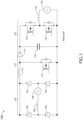
- FIG. 1 is a circuit diagram of a conventional apparatus 100 for AC to AC frequency conversion.
- the apparatus includes a rectifier 102 that converts an input alternating current (generated by source 108) to a direct current (DC).
- the rectifier 102 includes an inductor 106 and a plurality of diodes 104.
- a boost converter 110 steps up the DC voltage.
- the boost converter 110 includes an inductor 112, a diode 114, a transistor 116, and a capacitor 118.
- an inverter 120 converts the DC back to an output AC (represented by output AC load 126).
- the inverter 120 includes two transistors 122 and an inductor 125.
- the conventional apparatus 100 includes multiple different power conversion stages (the rectifier 102, the boost converter 110, and the inverter 120). Since each conversion stage is fixed in design, the conventional apparatus 100 is difficult to customize for weight, volume and cost requirements of various applications (for example, different aircraft having different sizes). Thus, a customizable solution that solves the above problems is desirable.
- Embodiments of the present disclosure are directed to an apparatus for modular AC to AC frequency conversion.
- the present apparatus includes high frequency (HF) conversion stages and low frequency (LF) conversion stages that are modular.
- the conversion stages e.g., modules or building blocks
- the conversion stages are attachable and detachable to the circuit, such that units can be added and removed based on the power and frequency requirements of a particular application (which can vary between each customer, e.g., different aircraft having different sizes, different amounts of aircraft seats, etc.).
- FIG. 2 is a circuit diagram of an HF conversion stage 200, in accordance with one or more embodiments of the present disclosure.
- the current is then rectified by two parallel switches S 1 and S 2 to generate a DC output voltage V out .
- the inductor L b is configured to remove ripple in the DC current due to incomplete suppression of the alternating waveform after rectification.
- the switches S 1 and S 2 may be controlled by pulse-width-modulation (PWM) using a PWM signal and a PWM controller.
- PWM controls (e.g., reduces) the average power delivered by the current by partitioning the signal into discrete parts.
- the average value of voltage and current fed to the load is controlled by turning the switches S 1 and S 2 between supply (V in ) and load (V out ) on and off at a fast rate.
- the PWM switching frequency has to be high enough not to affect the load V out such that the resultant waveform perceived by the load is smooth (continuous).
- the PWM-controlled switching frequency of the switches S 1 and S 2 may be of from 10 KHz to 1000 KHz, and may be adjusted depending on the target voltage and target converted frequency of a particular application.
- the switches S 1 and S 2 comprise high electron mobility transistors (HEMTs), also known as heterostructure field effect transistors (HFETs) or modulation-doped field effect transistors (MODFETs).
- HEMTs are field-effect transistors that include a junction between two materials with different band gaps (i.e., a heterojunction) as the channel instead of a doped region (as is generally the case for a MOSFET).
- the switches S 1 and S 2 may comprise gallium nitride (GaN) based HEMTs (e.g., for lower voltage applications).
- the switches S 1 and S 2 may comprise silicon carbide (SiC) based HEMTs (e.g., for higher voltage applications).
- FIG. 3 is a circuit diagram of an LF conversion stage 300, in accordance with one or more embodiments of the present disclosure.
- the current is then rectified by two parallel switches S 3 and S 4 to generate a DC output voltage V out
- the inductor L b is configured to remove ripple in the DC current due to incomplete suppression of the alternating waveform after rectification.
- the switches S 3 and S 4 may have a switching frequency of from 10 Hz to 1 KHz (i.e., orders of magnitude lower than the switching rate of the PWM-controlled switches S 1 and S 2 of the HF conversion stage 200).
- the LF conversion stage 300 when arranged in parallel with one or more HF conversion stages 200, may be configured to return current from the HF conversion stages 200.
- the switches S 3 and S 4 may comprise silicon (Si) based metal-oxide-semiconductor field effect transistors (MOSFETs). Although the switches S 3 and S 4 may also be GaN based or SiC based (e.g., for high performance), using Si based switches S 3 and S 4 for the LF conversion stage 300 may reduce cost significantly when paired with switches S 1 and S 2 for the HF conversion stage 200 that are GaN based or SiC based (since GaN and SiC are relatively expensive compared to Si).
- Si silicon
- MOSFETs metal-oxide-semiconductor field effect transistors
- the switches S 3 and S 4 may comprise power MOSFETs.
- a power MOSFET may have a vertical diffused MOS (VDMOS) structure (also called double-diffused MOS or DMOS).
- VDMOS vertical diffused MOS
- the source electrode is placed over the drain, resulting in a current mainly vertical when the transistor is in the on-state.
- the voltage rating of the transistor is a function of the doping and thickness of the N epitaxial layer, while the current rating is a function of the channel width. This vertical structure makes it possible for the transistor to sustain both high blocking voltage and high current within a compact piece of silicon.
- the power MOSFET When the power MOSFET is in the on-state, the power MOSFET exhibits a resistive behavior between the drain and source terminals.
- the power MOSFET is equivalent to a PIN diode.
- the switches S 3 and S 4 may comprise super junction MOSFETs.
- a super junction MOSFET the N layer and P layers are arranged as vertical trenches in the drift layer, so that when voltage is applied, the depletion layers expand horizontally, and soon merge to form a depletion layer equal to the depth of the trenches.
- the depletion layer only expands to half the pitch of the trenches, so a depletion layer is formed with a thickness equal to the depth of the trenches.
- the expansion of the depletion layer is small, allowing for an approximately 5 times increase in the drift layer impurity concentration.
- FIG. 4 is a circuit diagram of a modular AC to AC frequency conversion apparatus 400, in accordance with one or more embodiments of the present disclosure.
- One or more primary HF conversion stages 200a and one or more primary LF conversion stages 300a are configured to convert an input AC voltage V in to an intermediate DC voltage V dc .
- One or more secondary HF conversion stages 200a and one or more secondary LF conversion stages 300a are configured to convert the intermediate DC voltage V dc to an output AC voltage V out
- An input AC source (e.g., generator) may be configured to generate an input AC voltage V in at a first frequency.
- the input AC source may be, for example, an aircraft power supply.
- the first frequency may be, for example, of from 300 Hz to 750 Hz. This first frequency may be significantly higher than the operating frequency of household and portable electronics that may be used by passengers (for example, 50 Hz or 60 Hz), and thus, may be converted to the appropriate frequency (e.g, to power an electrical outlet or USB port at an aircraft seat) using the apparatus 400.
- the one or more primary HF conversion stages 200a may be substantially identical to the HF conversion stage 200 described with respect to FIG. 2 .
- Each HF conversion stage 200a may comprise a first pair of HEMTs S 1 and S 2 (controlled by PWM as described with respect to FIG. 2 ).
- At least one HF input AC voltage terminal 402 may be respectively connected to the input AC source.
- At least one inductor L b,1 may be respectively connected to the one or more primary HF conversion stages 200a (using the terminal 402) and the input AC source.
- the one or more primary LF conversion stages 300a may be substantially identical to the LF conversion stage 300 described with respect to FIG. 3 .
- Each LF conversion stage 300a may comprise a first pair of MOSFETs S 3 and S 4 .
- At least one LF input AC voltage terminal 404 may be respectively connected to the input AC source.
- At least one inductor L b,2 may be respectively connected to the one or more primary LF conversion stages 300a (using the terminal 404) and the input AC source.
- At least two output DC voltage terminals 406 may be configured to receive the intermediate DC voltage V dc generated by the conversion stages 200a and 300a.
- the switch S 1 may be connected in parallel with the switch S 3 to one of the terminals 406, and the switch S 2 may be connected in parallel with the switch S 4 to the other of the terminals 406.
- a capacitor C dc may be configured to store energy of the intermediate DC voltage V dc .
- At least two input DC voltage terminals 408 may be configured to receive the intermediate DC voltage V db from the output DC voltage terminals 406.
- Each of the terminals 408 may be connected to a respective one of the terminals 406, and the capacitor C dc may bridge the connections between the terminals 406 and 408.
- the terminals 408 may be configured to transmit the intermediate DC voltage V dc to the one or more secondary HF conversion stages 200b and the one or more secondary LF conversion stages 300b.
- the one or more secondary HF conversion stages 200b may be substantially identical to the HF conversion stage 200 described with respect to FIG. 2 , and may be configured to convert the intermediate DC voltage V dc to an output AC voltage V out .
- Each HF conversion stage 200a may comprise a second pair of HEMTs S 3 and S 6 (controlled by PWM as described with respect to FIG. 2 ).
- At least one HF output AC voltage terminal 410 may be respectively connected to an output AC load.
- At least one inductor L o,1 may be respectively connected to the one or more secondary HF conversion stages 200b (using the terminal 410) and the output AC load.
- the one or more secondary LF conversion stages 300b may be substantially identical to the HF conversion stage 300 described with respect to FIG. 3 , and may be configured to convert the intermediate DC voltage V dc to an output AC voltage V out .
- Each LF conversion stage 300b may comprise a second pair of MOSFETs S 7 and S 8 .
- At least one LF output AC voltage terminal 412 may be respectively connected to an output AC load.
- At least one inductor L o,2 may be respectively connected to the one or more secondary HF conversion stages 300b (using the terminal 412) and the output AC load.
- the switch S 5 is connected in parallel with the switch S 7 to one of the terminals 408, and the switch S 6 is connected in parallel with the switch S 8 to the other of the terminals 408.
- the AC voltage V out may have a target power and a target frequency (e.g., 50 or 60 Hz).
- the output AC load is a plurality of aircraft seat power supplies, and each secondary HF conversion stage 200 may correspond to an aircraft seat (or a row or section of aircraft seats).
- the present disclosure is not limited thereto, and the output AC load may include, for example, an aircraft oven, an aircraft microwave, etc.
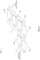
- FIG. 5 is a simplified diagram of a modular AC to AC frequency conversion apparatus 500, in accordance with one or more embodiments of the present disclosure.
- the apparatus 500 may be substantially identical to the apparatus 400 described with respect to FIG. 4 , however, the apparatus 500 may include additional secondary HF conversion stages 200c and 200d (connected in parallel with the secondary HF conversion stage 200b and the secondary LF conversion stage 300b).
- the conversion stages 200 and 300 may be modular (attachable and detachable to the circuit, such that conversion stages 200 and 300 can be added to the apparatus 500 or removed from the apparatus 500 based on the power and frequency requirements).
- Each conversion stage may be designed to use a filter inductor with the same rating, regardless of how many conversion stages are installed to meet a particular power level requirement.
- the present apparatus achieves a higher efficiency and a higher power density over the conventional solution.
- the modular capability of the present apparatus enables frequency conversion for varying power supply applications without having to constantly design new converter components, thus reducing costs while improving performance in weight, size, loss, and temperature control.
Landscapes
- Engineering & Computer Science (AREA)
- Power Engineering (AREA)
- Mechanical Engineering (AREA)
- Rectifiers (AREA)
Abstract
Description
- Electrical power supplies in aerospace applications are characterized by a wide range of stringent requirements. Examples of such power supplies include alternating current (AC) to AC power supplies that convert power from a higher frequency, such as 300 Hz, to a lower frequency, such as 60 Hz. Conventional AC-to-AC power supplies include multiple power conversion stages that are difficult to customize for target applications, and are thus larger, heavier, difficult to scale, and expensive to manufacture.
- An apparatus for modular AC to AC frequency conversion is disclosed in accordance with one or more illustrative embodiments of the present disclosure. The apparatus comprises an input AC source configured to generate an input AC voltage at a first frequency; at least one low frequency (LF) input AC voltage terminal connected to the input AC source; at least one high frequency (HF) input AC voltage terminal connected to the input AC source; at least two output DC voltage terminals; at least one primary LF conversion stage configured to receive the input AC voltage at the first frequency and generate a DC voltage, comprising: a first pair of metal-oxide-semiconductor field effect transistors (MOSFETs) connected to the at least one LF input AC voltage terminal and the at least two output DC voltage terminals; at least one primary HF conversion stage configured to receive the input AC voltage at the first frequency and generate the DC voltage, comprising: a first pair of high electron mobility transistors (HEMTs) connected to the at least one HF input AC voltage terminal and the at least two output DC voltage terminals; a capacitor configured to store energy of the DC voltage; at least two input DC voltage terminals, wherein each of the input DC voltage terminals are connected to a respective one of the output DC voltage terminals; at least one LF output AC voltage terminal; at least one HF output AC voltage terminal; at least one secondary LF conversion stage configured to receive the DC voltage and generate an output AC voltage at a second frequency, comprising: a second pair of MOSFETs connected to the at least two input DC voltage terminals and the at least one LF output AC voltage terminal; at least one secondary HF conversion stage configured to receive the DC voltage and generate the output AC voltage at the second frequency, comprising: a second pair of HEMTs connected to the at least two input DC voltage terminals and the at least one HF output AC voltage terminal; and an output AC load configured to receive the output AC voltage at the second frequency.
- It is to be understood that both the foregoing general description and the following detailed description are exemplary and explanatory only and are not necessarily restrictive of the invention as claimed. The accompanying drawings, which are incorporated in and constitute a part of the specification, illustrate embodiments of the invention and together with the general description, serve to explain the principles of the invention.
- The numerous advantages of the disclosure may be better understood by those skilled in the art by reference to the accompanying figures in which:
-
FIG. 1 is a circuit diagram of a conventional apparatus for AC to AC frequency conversion. -
FIG. 2 is a circuit diagram of a high frequency conversion stage, in accordance with one or more embodiments of the present disclosure. -
FIG. 3 is a circuit diagram of a low frequency conversion stage, in accordance with one or more embodiments of the present disclosure. -
FIG. 4 is a circuit diagram of a modular AC to AC frequency conversion apparatus, in accordance with one or more embodiments of the present disclosure. -
FIG. 5 is a simplified diagram of a modular AC to AC frequency conversion apparatus including additional HF conversion stages, in accordance with one or more embodiments of the present disclosure. - Before explaining at least one embodiment of the inventive concepts disclosed herein in detail, it is to be understood that the inventive concepts are not limited in their application to the details of construction and the arrangement of the components or steps or methodologies set forth in the following description or illustrated in the drawings. In the following detailed description of embodiments of the present disclosure, numerous specific details are set forth in order to provide a more thorough understanding of the inventive concepts. However, it will be apparent to one of ordinary skill in the art having the benefit of the present disclosure that the inventive concepts disclosed herein may be practiced without these specific details. In other instances, well-known features may not be described in detail to avoid unnecessarily complicating the present disclosure. The inventive concepts disclosed herein are capable of other embodiments or of being practiced or carried out in various ways. Also, it is to be understood that the phraseology and terminology employed herein is for the purpose of description and should not be regarded as limiting.
- As used herein a letter following a reference numeral is intended to reference an embodiment of the feature or element that may be similar, but not necessarily identical, to a previously described element or feature bearing the same reference numeral (e.g., 1, 1a, 1b). Such shorthand notations are used for purposes of convenience only, and should not be construed to limit the inventive concepts disclosed herein in any way unless expressly stated to the contrary. Further, unless expressly stated to the contrary, "or" refers to an inclusive or and not to an exclusive or. For example, a condition A or B is satisfied by any one of the following: A is true (or present) and B is false (or not present), A is false (or not present) and B is true (or present), and both A and B are true (or present). In addition, use of the "a" or "an" are employed to describe elements and components of embodiments of the present inventive concepts. This is done merely for convenience and to give a general sense of the inventive concepts, and "a" and "an" are intended to include one or at least one and the singular also includes the plural unless it is obvious that it is meant otherwise.
- Finally, as used herein any reference to "one embodiment" or "some embodiments" means that a particular element, feature, structure, or characteristic described in connection with the embodiment is included in at least one embodiment of the inventive concepts disclosed herein. The appearances of the phrase "in some embodiments" in various places in the specification are not necessarily all referring to the same embodiment, and embodiments of the inventive concepts disclosed may include one or more of the features expressly described or inherently present herein, or any combination or sub-combination of two or more such features, along with any other features which may not necessarily be expressly described or inherently present in the present disclosure.
- Electrical power supplies used in aerospace applications (e.g., aircraft seat power supplies) are characterized by a wide range of stringent requirements, stemming from various implementation constraints of the end product. For example, an electrical power supply may contribute to the overall weight of an aircraft, and is therefore ideally designed to be as light as possible. Each customer of such power supplies may have different requirements (e.g., depending on the type of aircraft).
- Conventional AC-to-AC power supplies (e.g., that convert AC current at a first frequency to an AC current at a second frequency) include multiple power conversion stages that are difficult to customize for target applications, and are thus larger, heavier, difficult to scale, and expensive to manufacture. When implementing the conventional solution, the equipment manufacturer must either produce an individual, optimal design for each customer, thus increasing the development cost for each product, or produce an over-designed product that may not be competitive in terms of volume or weight compared to competing devices.
-
FIG. 1 is a circuit diagram of aconventional apparatus 100 for AC to AC frequency conversion. The apparatus includes arectifier 102 that converts an input alternating current (generated by source 108) to a direct current (DC). Therectifier 102 includes aninductor 106 and a plurality ofdiodes 104. Aboost converter 110 steps up the DC voltage. Theboost converter 110 includes aninductor 112, adiode 114, atransistor 116, and acapacitor 118. Finally, aninverter 120 converts the DC back to an output AC (represented by output AC load 126). Theinverter 120 includes twotransistors 122 and an inductor 125. - The
conventional apparatus 100 includes multiple different power conversion stages (therectifier 102, theboost converter 110, and the inverter 120). Since each conversion stage is fixed in design, theconventional apparatus 100 is difficult to customize for weight, volume and cost requirements of various applications (for example, different aircraft having different sizes). Thus, a customizable solution that solves the above problems is desirable. - Embodiments of the present disclosure are directed to an apparatus for modular AC to AC frequency conversion. The present apparatus includes high frequency (HF) conversion stages and low frequency (LF) conversion stages that are modular. In this way, the conversion stages (e.g., modules or building blocks) are attachable and detachable to the circuit, such that units can be added and removed based on the power and frequency requirements of a particular application (which can vary between each customer, e.g., different aircraft having different sizes, different amounts of aircraft seats, etc.).
-
FIG. 2 is a circuit diagram of anHF conversion stage 200, in accordance with one or more embodiments of the present disclosure. After the input voltage Vin passes a inductor Lb, the current is then rectified by two parallel switches S1 and S2 to generate a DC output voltage Vout. The inductor Lb is configured to remove ripple in the DC current due to incomplete suppression of the alternating waveform after rectification. - The switches S1 and S2 may be controlled by pulse-width-modulation (PWM) using a PWM signal and a PWM controller. PWM controls (e.g., reduces) the average power delivered by the current by partitioning the signal into discrete parts. The average value of voltage and current fed to the load is controlled by turning the switches S1 and S2 between supply (Vin) and load (Vout) on and off at a fast rate. The longer the switches S1 and S2 on compared to the off periods, the higher the total power supplied to the load Vout. The PWM switching frequency has to be high enough not to affect the load Vout such that the resultant waveform perceived by the load is smooth (continuous). In some embodiments, the PWM-controlled switching frequency of the switches S1 and S2 may be of from 10 KHz to 1000 KHz, and may be adjusted depending on the target voltage and target converted frequency of a particular application.
- In some embodiments, the switches S1 and S2 comprise high electron mobility transistors (HEMTs), also known as heterostructure field effect transistors (HFETs) or modulation-doped field effect transistors (MODFETs). HEMTs are field-effect transistors that include a junction between two materials with different band gaps (i.e., a heterojunction) as the channel instead of a doped region (as is generally the case for a MOSFET). In some embodiments, the switches S1 and S2 may comprise gallium nitride (GaN) based HEMTs (e.g., for lower voltage applications). In some embodiments, the switches S1 and S2 may comprise silicon carbide (SiC) based HEMTs (e.g., for higher voltage applications).
-
FIG. 3 is a circuit diagram of anLF conversion stage 300, in accordance with one or more embodiments of the present disclosure. After the input voltage Vin passes a inductor Lb, the current is then rectified by two parallel switches S3 and S4 to generate a DC output voltage Vout The inductor Lb is configured to remove ripple in the DC current due to incomplete suppression of the alternating waveform after rectification. The switches S3 and S4 may have a switching frequency of from 10 Hz to 1 KHz (i.e., orders of magnitude lower than the switching rate of the PWM-controlled switches S1 and S2 of the HF conversion stage 200). TheLF conversion stage 300, when arranged in parallel with one or more HF conversion stages 200, may be configured to return current from the HF conversion stages 200. - In some embodiments, the switches S3 and S4 may comprise silicon (Si) based metal-oxide-semiconductor field effect transistors (MOSFETs). Although the switches S3 and S4 may also be GaN based or SiC based (e.g., for high performance), using Si based switches S3 and S4 for the
LF conversion stage 300 may reduce cost significantly when paired with switches S1 and S2 for theHF conversion stage 200 that are GaN based or SiC based (since GaN and SiC are relatively expensive compared to Si). - In some embodiments, the switches S3 and S4 may comprise power MOSFETs. A power MOSFET may have a vertical diffused MOS (VDMOS) structure (also called double-diffused MOS or DMOS). In a VDMOS, the source electrode is placed over the drain, resulting in a current mainly vertical when the transistor is in the on-state. With a vertical structure, the voltage rating of the transistor is a function of the doping and thickness of the N epitaxial layer, while the current rating is a function of the channel width. This vertical structure makes it possible for the transistor to sustain both high blocking voltage and high current within a compact piece of silicon. When the power MOSFET is in the on-state, the power MOSFET exhibits a resistive behavior between the drain and source terminals. When the power MOSFET is in the off-state, the power MOSFET is equivalent to a PIN diode.
- In some embodiments, the switches S3 and S4 may comprise super junction MOSFETs. In a super junction MOSFET, the N layer and P layers are arranged as vertical trenches in the drift layer, so that when voltage is applied, the depletion layers expand horizontally, and soon merge to form a depletion layer equal to the depth of the trenches. The depletion layer only expands to half the pitch of the trenches, so a depletion layer is formed with a thickness equal to the depth of the trenches. The expansion of the depletion layer is small, allowing for an approximately 5 times increase in the drift layer impurity concentration.
-
FIG. 4 is a circuit diagram of a modular AC to ACfrequency conversion apparatus 400, in accordance with one or more embodiments of the present disclosure. One or more primary HF conversion stages 200a and one or more primaryLF conversion stages 300a are configured to convert an input AC voltage Vin to an intermediate DC voltage Vdc. One or more secondary HF conversion stages 200a and one or more secondaryLF conversion stages 300a are configured to convert the intermediate DC voltage Vdc to an output AC voltage Vout - An input AC source (e.g., generator) may be configured to generate an input AC voltage Vin at a first frequency. The input AC source may be, for example, an aircraft power supply. The first frequency may be, for example, of from 300 Hz to 750 Hz. This first frequency may be significantly higher than the operating frequency of household and portable electronics that may be used by passengers (for example, 50 Hz or 60 Hz), and thus, may be converted to the appropriate frequency (e.g, to power an electrical outlet or USB port at an aircraft seat) using the
apparatus 400. - The one or more primary
HF conversion stages 200a may be substantially identical to theHF conversion stage 200 described with respect toFIG. 2 . EachHF conversion stage 200a may comprise a first pair of HEMTs S1 and S2 (controlled by PWM as described with respect toFIG. 2 ). At least one HF inputAC voltage terminal 402 may be respectively connected to the input AC source. At least one inductor Lb,1 may be respectively connected to the one or more primary HF conversion stages 200a (using the terminal 402) and the input AC source. - The one or more primary
LF conversion stages 300a may be substantially identical to theLF conversion stage 300 described with respect toFIG. 3 . EachLF conversion stage 300a may comprise a first pair of MOSFETs S3 and S4. At least one LF inputAC voltage terminal 404 may be respectively connected to the input AC source. At least one inductor Lb,2 may be respectively connected to the one or more primary LF conversion stages 300a (using the terminal 404) and the input AC source. - At least two output
DC voltage terminals 406 may be configured to receive the intermediate DC voltage Vdc generated by the conversion stages 200a and 300a. In some embodiments, the switch S1 may be connected in parallel with the switch S3 to one of theterminals 406, and the switch S2 may be connected in parallel with the switch S4 to the other of theterminals 406. - In some embodiments, a capacitor Cdc may be configured to store energy of the intermediate DC voltage Vdc. At least two input
DC voltage terminals 408 may be configured to receive the intermediate DC voltage Vdb from the outputDC voltage terminals 406. Each of theterminals 408 may be connected to a respective one of theterminals 406, and the capacitor Cdc may bridge the connections between theterminals terminals 408 may be configured to transmit the intermediate DC voltage Vdc to the one or more secondary HF conversion stages 200b and the one or more secondary LF conversion stages 300b. - The one or more secondary HF conversion stages 200b may be substantially identical to the
HF conversion stage 200 described with respect toFIG. 2 , and may be configured to convert the intermediate DC voltage Vdc to an output AC voltage Vout. EachHF conversion stage 200a may comprise a second pair of HEMTs S3 and S6 (controlled by PWM as described with respect toFIG. 2 ). At least one HF outputAC voltage terminal 410 may be respectively connected to an output AC load. At least one inductor Lo,1 may be respectively connected to the one or more secondary HF conversion stages 200b (using the terminal 410) and the output AC load. - The one or more secondary LF conversion stages 300b may be substantially identical to the
HF conversion stage 300 described with respect toFIG. 3 , and may be configured to convert the intermediate DC voltage Vdc to an output AC voltage Vout. EachLF conversion stage 300b may comprise a second pair of MOSFETs S7 and S8. At least one LF outputAC voltage terminal 412 may be respectively connected to an output AC load. At least one inductor Lo,2 may be respectively connected to the one or more secondary HF conversion stages 300b (using the terminal 412) and the output AC load. - In some embodiments, the switch S5 is connected in parallel with the switch S7 to one of the
terminals 408, and the switch S6 is connected in parallel with the switch S8 to the other of theterminals 408. After exiting the secondary conversion stages 200b and 300b, the AC voltage Vout may have a target power and a target frequency (e.g., 50 or 60 Hz). In some embodiments, the output AC load is a plurality of aircraft seat power supplies, and each secondaryHF conversion stage 200 may correspond to an aircraft seat (or a row or section of aircraft seats). However, the present disclosure is not limited thereto, and the output AC load may include, for example, an aircraft oven, an aircraft microwave, etc. -
FIG. 5 is a simplified diagram of a modular AC to ACfrequency conversion apparatus 500, in accordance with one or more embodiments of the present disclosure. Theapparatus 500 may be substantially identical to theapparatus 400 described with respect toFIG. 4 , however, theapparatus 500 may include additional secondary HF conversion stages 200c and 200d (connected in parallel with the secondaryHF conversion stage 200b and the secondaryLF conversion stage 300b). In this way, the conversion stages 200 and 300 may be modular (attachable and detachable to the circuit, such that conversion stages 200 and 300 can be added to theapparatus 500 or removed from theapparatus 500 based on the power and frequency requirements). Each conversion stage may be designed to use a filter inductor with the same rating, regardless of how many conversion stages are installed to meet a particular power level requirement. - The present apparatus achieves a higher efficiency and a higher power density over the conventional solution. The modular capability of the present apparatus enables frequency conversion for varying power supply applications without having to constantly design new converter components, thus reducing costs while improving performance in weight, size, loss, and temperature control.
- It is believed that the present disclosure and many of its attendant advantages will be understood by the foregoing description, and it will be apparent that various changes may be made in the form, construction, and arrangement of the components without departing from the scope of the invention as defined by the appended claims.
Claims (15)
- An apparatus for modular alternating current, AC, to AC frequency conversion, comprising:an input AC source (108) configured to generate an input AC voltage at a first frequency;at least one low frequency, LF, input AC voltage terminal (404) connected to the input AC source;at least one high frequency, HF, input AC voltage terminal connected to the input AC source;at least two output DC voltage terminals (406);at least one primary LF conversion stage (300) configured to receive the input AC voltage at the first frequency and generate a DC voltage, comprising:
a first pair of metal-oxide-semiconductor field effect transistors, MOSFETs, connected to the at least one LF input AC voltage terminal and the at least two output DC voltage terminals;at least one primary HF conversion stage (200) configured to receive the input AC voltage at the first frequency and generate the DC voltage, comprising:
a first pair of high electron mobility transistors, HEMTs, connected to the at least one HF input AC voltage terminal and the at least two output DC voltage terminals;a capacitor configured to store energy of the DC voltage;at least two input DC voltage terminals, wherein each of the input DC voltage terminals are connected to a respective one of the output DC voltage terminals;at least one LF output AC voltage terminal (412);at least one HF output AC voltage terminal (410);at least one secondary LF conversion stage configured to receive the DC voltage and generate an output AC voltage at a second frequency, comprising:
a second pair of MOSFETs connected to the at least two input DC voltage terminals and the at least one LF output AC voltage terminal;at least one secondary HF conversion stage configured to receive the DC voltage and generate the output AC voltage at the second frequency, comprising:
a second pair of HEMTs connected to the at least two input DC voltage terminals and the at least one HF output AC voltage terminal; andan output AC load configured to receive the output AC voltage at the second frequency. - The apparatus of claim 1, comprising at least one inductor connected to the at least one primary LF conversion stage and the input AC source, and at least one inductor connected to the at least one primary HF conversion stage and the input AC source.
- The apparatus of claim 1 or 2, comprising at least one inductor connected to the at least one secondary LF conversion stage and the output AC load, and at least one inductor connected to the at least one secondary HF conversion stage and the output AC load.
- The apparatus of any preceding claim, wherein the at least one primary LF conversion stage comprises a plurality of primary LF conversion stages.
- The apparatus of any preceding claim, wherein the at least one primary HF conversion stage comprises a plurality of primary HF conversion stages.
- The apparatus of any preceding claim, wherein the at least one secondary LF conversion stage comprises a plurality of secondary LF conversion stages.
- The apparatus of any preceding claim, wherein the at least one secondary HF conversion stage comprises a plurality of secondary HF conversion stages.
- The apparatus of any preceding claim, wherein the first pair of MOSFETs and the second pair of MOSFETS comprise silicon, Si, based power MOSFETs.
- The apparatus of any preceding claim, wherein the first pair of MOSFETs and the second pair of MOSFETS comprise silicon, Si, based super junction MOSFETs.
- The apparatus of any preceding claim, wherein the first pair of HEMTs and the second pair of HEMTS comprise silicon carbide, SiC, based HEMTs.
- The apparatus of any preceding claim, wherein the first pair of HEMTs and the second pair of HEMTS comprise gallium nitride, GaN, based HEMTs.
- The apparatus of any preceding claim, wherein the first frequency is of from 300 to 750 Hz, and the second frequency is of from 50-60 Hz.
- The apparatus of any preceding claim, wherein the input AC source is an aircraft power supply, and the output AC load is a plurality of aircraft seat power supplies.
- The apparatus of any preceding claim, wherein the first pair of MOSFETs and the second pair of MOSFETS have a switching frequency of from 10 Hz to 1 KHz.
- The apparatus of any preceding claim, wherein the first pair of HEMTs and the second pair of HEMTS have a pulse width modulated, PWM, switching frequency of from 10 KHz to 1000 KHz.
Applications Claiming Priority (1)
| Application Number | Priority Date | Filing Date | Title |
|---|---|---|---|
| US17/496,481 US11532993B1 (en) | 2021-10-07 | 2021-10-07 | AC-to-AC power supplies using multi-frequency power conversion building blocks |
Publications (1)
| Publication Number | Publication Date |
|---|---|
| EP4164108A1 true EP4164108A1 (en) | 2023-04-12 |
Family
ID=83689399
Family Applications (1)
| Application Number | Title | Priority Date | Filing Date |
|---|---|---|---|
| EP22200409.5A Withdrawn EP4164108A1 (en) | 2021-10-07 | 2022-10-07 | Ac-to-ac power supplies using multi-frequency power conversion building blocks |
Country Status (2)
| Country | Link |
|---|---|
| US (1) | US11532993B1 (en) |
| EP (1) | EP4164108A1 (en) |
Families Citing this family (1)
| Publication number | Priority date | Publication date | Assignee | Title |
|---|---|---|---|---|
| US20250253094A1 (en) | 2024-02-02 | 2025-08-07 | Rockwell Collins, Inc. | Radiation hardened active power transformer |
Citations (2)
| Publication number | Priority date | Publication date | Assignee | Title |
|---|---|---|---|---|
| CN110445410A (en) * | 2019-08-13 | 2019-11-12 | 成都飞机工业(集团)有限责任公司 | A kind of more closed loops of aircraft are for electric regulating system and power supply adjusting method |
| US20200259438A1 (en) * | 2017-08-17 | 2020-08-13 | Jing-Jin Electric Technologies Co., Ltd. | Multi-inverter electronic motor controller |
Family Cites Families (15)
| Publication number | Priority date | Publication date | Assignee | Title |
|---|---|---|---|---|
| US3566243A (en) | 1968-09-30 | 1971-02-23 | Pillar Corp | High frequency power supply |
| IT1111993B (en) | 1979-03-06 | 1986-01-13 | Venturini Marco | DIRECT AC / AC FREQUENCY CONVERTER |
| JPS61240856A (en) | 1985-04-17 | 1986-10-27 | Tdk Corp | Ac/ac converter |
| FR2700081B1 (en) | 1992-12-30 | 1995-01-27 | Unite Hermetique Sa | Structure of a static frequency converter. |
| KR100342457B1 (en) | 1994-02-10 | 2002-11-02 | 코닌클리케 필립스 일렉트로닉스 엔.브이. | High frequency ac/ac converter with power factor correction |
| WO2000057543A1 (en) | 1999-03-23 | 2000-09-28 | Advanced Energy Industries, Inc. | High frequency switch-mode dc powered computer system |
| US6466464B1 (en) | 1999-05-14 | 2002-10-15 | Intel Corporation | Method and apparatus for high frequency alternating current power distribution |
| US9800167B2 (en) * | 2014-02-07 | 2017-10-24 | Abb Schweiz Ag | Multi-phase AC/AC step-down converter for distribution systems |
| CN108054925A (en) | 2015-06-23 | 2018-05-18 | 张琴 | Supply unit and method of work based on phase-shifting carrier wave technology reactive filter |
| EP3223419B1 (en) | 2016-03-22 | 2019-05-01 | GE Energy Power Conversion Technology Ltd | Direct ac-ac converter assembly and conversion system using same |
| AU2017202202A1 (en) * | 2016-09-09 | 2018-03-29 | Edge Electrons Limited | Series ac voltage regulator |
| SE544016C2 (en) | 2016-09-28 | 2021-11-02 | Abb Power Grids Switzerland Ag | Power unbalance compensation in ac/ac mmc |
| US9919610B1 (en) | 2017-01-12 | 2018-03-20 | The Florida International University Board Of Trustees | Wireless power electronics and controls |
| CN110611460B (en) | 2019-09-10 | 2020-11-06 | 东南大学 | High-power motor drive system based on modular multilevel inverter |
| CN115053440A (en) | 2019-12-24 | 2022-09-13 | 苏迪普.K.马祖姆德 | Solid state power conversion system |
-
2021
- 2021-10-07 US US17/496,481 patent/US11532993B1/en active Active
-
2022
- 2022-10-07 EP EP22200409.5A patent/EP4164108A1/en not_active Withdrawn
Patent Citations (2)
| Publication number | Priority date | Publication date | Assignee | Title |
|---|---|---|---|---|
| US20200259438A1 (en) * | 2017-08-17 | 2020-08-13 | Jing-Jin Electric Technologies Co., Ltd. | Multi-inverter electronic motor controller |
| CN110445410A (en) * | 2019-08-13 | 2019-11-12 | 成都飞机工业(集团)有限责任公司 | A kind of more closed loops of aircraft are for electric regulating system and power supply adjusting method |
Non-Patent Citations (2)
| Title |
|---|
| BUTICCHI GIAMPAOLO ET AL: "On-Board Microgrids for the More Electric Aircraft-Technology Review", IEEE TRANSACTIONS ON INDUSTRIAL ELECTRONICS, IEEE SERVICE CENTER, PISCATAWAY, NJ, USA, vol. 66, no. 7, July 2019 (2019-07-01), pages 5588 - 5599, XP011712607, ISSN: 0278-0046, [retrieved on 20190301], DOI: 10.1109/TIE.2018.2881951 * |
| DAVID REUSCH ET AL: "Gallium Nitride based 3D integrated non-isolated point of load module", APPLIED POWER ELECTRONICS CONFERENCE AND EXPOSITION (APEC), 2012 TWENTY-SEVENTH ANNUAL IEEE, IEEE, 5 February 2012 (2012-02-05), pages 38 - 45, XP032127647, ISBN: 978-1-4577-1215-9, DOI: 10.1109/APEC.2012.6165796 * |
Also Published As
| Publication number | Publication date |
|---|---|
| US11532993B1 (en) | 2022-12-20 |
Similar Documents
| Publication | Publication Date | Title |
|---|---|---|
| US9548668B2 (en) | Hybrid power converter and method | |
| US11967895B2 (en) | High efficiency power converting apparatus | |
| US10554141B2 (en) | Parallel hybrid converter apparatus and method | |
| US11075576B2 (en) | Apparatus and method for efficient shutdown of adiabatic charge pumps | |
| US11563337B2 (en) | High efficiency wireless charging system and method | |
| US9461554B2 (en) | Hybrid converter using a resonant stage and a non-isolated stage | |
| US9595877B2 (en) | Secondary side hybrid converter apparatus and method | |
| US9787200B2 (en) | Resonant converters with synchronous rectifier feedback | |
| US9812977B2 (en) | Resonant converters with an improved voltage regulation range | |
| US6861828B2 (en) | Apparatus and circuit for power supply, and apparatus for controlling large current load | |
| US9350260B2 (en) | Startup method and system for resonant converters | |
| US9520798B2 (en) | Multi-level DC-DC converter with galvanic isolation and adaptive conversion ratio | |
| EP2840695A1 (en) | Power conversion device, motor drive control apparatus provided with power conversion device, air blower and compressor provided with motor drive control apparatus, and air conditioner provided with air blower or compressor | |
| US11223237B2 (en) | High efficiency power converting apparatus and control method | |
| CN102959843A (en) | DC-DC power conversion apparatus | |
| KR20160029725A (en) | Bidirectional dc-to-dc converter | |
| US7298123B2 (en) | Apparatus and circuit for power supply, and apparatus for controlling large current load | |
| CN112615530B (en) | Controller circuit and method for generating pulse width modulation (PWM) signals | |
| EP2937982A2 (en) | Switch configuration for a matrix convertor | |
| CN110383662A (en) | Power conversion device | |
| US11532993B1 (en) | AC-to-AC power supplies using multi-frequency power conversion building blocks | |
| Rodriguez et al. | Optimizing the efficiency of a dc-dc boost converter over 98% by using commercial SiC transistors with switching frequencies from 100 kHz to 1MHz | |
| Toba et al. | Auxiliary resonant commutated pole inverter using two internal voltage-points of DC source | |
| Briere | The power electronics market and the status of GaN based power devices | |
| US12261547B2 (en) | Method of operating a power converter, control circuit, and power converter with switch input circuit |
Legal Events
| Date | Code | Title | Description |
|---|---|---|---|
| PUAI | Public reference made under article 153(3) epc to a published international application that has entered the european phase |
Free format text: ORIGINAL CODE: 0009012 |
|
| STAA | Information on the status of an ep patent application or granted ep patent |
Free format text: STATUS: THE APPLICATION HAS BEEN PUBLISHED |
|
| AK | Designated contracting states |
Kind code of ref document: A1 Designated state(s): AL AT BE BG CH CY CZ DE DK EE ES FI FR GB GR HR HU IE IS IT LI LT LU LV MC ME MK MT NL NO PL PT RO RS SE SI SK SM TR |
|
| STAA | Information on the status of an ep patent application or granted ep patent |
Free format text: STATUS: REQUEST FOR EXAMINATION WAS MADE |
|
| P01 | Opt-out of the competence of the unified patent court (upc) registered |
Effective date: 20230928 |
|
| 17P | Request for examination filed |
Effective date: 20231012 |
|
| RBV | Designated contracting states (corrected) |
Designated state(s): AL AT BE BG CH CY CZ DE DK EE ES FI FR GB GR HR HU IE IS IT LI LT LU LV MC ME MK MT NL NO PL PT RO RS SE SI SK SM TR |
|
| STAA | Information on the status of an ep patent application or granted ep patent |
Free format text: STATUS: EXAMINATION IS IN PROGRESS |
|
| 17Q | First examination report despatched |
Effective date: 20250425 |
|
| STAA | Information on the status of an ep patent application or granted ep patent |
Free format text: STATUS: THE APPLICATION IS DEEMED TO BE WITHDRAWN |
|
| 18D | Application deemed to be withdrawn |
Effective date: 20250826 |