EP4163987A1 - Magnetic field detection device and magnetic field detection device array - Google Patents
Magnetic field detection device and magnetic field detection device array Download PDFInfo
- Publication number
- EP4163987A1 EP4163987A1 EP21818582.5A EP21818582A EP4163987A1 EP 4163987 A1 EP4163987 A1 EP 4163987A1 EP 21818582 A EP21818582 A EP 21818582A EP 4163987 A1 EP4163987 A1 EP 4163987A1
- Authority
- EP
- European Patent Office
- Prior art keywords
- magnetic field
- field detection
- detection devices
- side surfaces
- engagement portion
- Prior art date
- Legal status (The legal status is an assumption and is not a legal conclusion. Google has not performed a legal analysis and makes no representation as to the accuracy of the status listed.)
- Pending
Links
- 238000001514 detection method Methods 0.000 title claims abstract description 125
- 230000007613 environmental effect Effects 0.000 claims description 17
- 230000000694 effects Effects 0.000 description 15
- 230000005389 magnetism Effects 0.000 description 13
- 238000004804 winding Methods 0.000 description 10
- 238000010586 diagram Methods 0.000 description 6
- 230000004048 modification Effects 0.000 description 6
- 238000012986 modification Methods 0.000 description 6
- 238000005259 measurement Methods 0.000 description 5
- 239000000758 substrate Substances 0.000 description 3
- 230000015572 biosynthetic process Effects 0.000 description 2
- 238000006073 displacement reaction Methods 0.000 description 2
- 239000000463 material Substances 0.000 description 2
- 239000011159 matrix material Substances 0.000 description 2
- 230000010355 oscillation Effects 0.000 description 2
- 230000002093 peripheral effect Effects 0.000 description 2
- 230000005415 magnetization Effects 0.000 description 1
- 230000000149 penetrating effect Effects 0.000 description 1
- 230000035699 permeability Effects 0.000 description 1
- 239000011347 resin Substances 0.000 description 1
- 229920005989 resin Polymers 0.000 description 1
- 230000035945 sensitivity Effects 0.000 description 1
- 229910000859 α-Fe Inorganic materials 0.000 description 1
Images







Classifications
-
- G—PHYSICS
- G01—MEASURING; TESTING
- G01R—MEASURING ELECTRIC VARIABLES; MEASURING MAGNETIC VARIABLES
- G01R33/00—Arrangements or instruments for measuring magnetic variables
- G01R33/0017—Means for compensating offset magnetic fields or the magnetic flux to be measured; Means for generating calibration magnetic fields
-
- G—PHYSICS
- G01—MEASURING; TESTING
- G01R—MEASURING ELECTRIC VARIABLES; MEASURING MAGNETIC VARIABLES
- G01R33/00—Arrangements or instruments for measuring magnetic variables
- G01R33/02—Measuring direction or magnitude of magnetic fields or magnetic flux
- G01R33/025—Compensating stray fields
-
- G—PHYSICS
- G01—MEASURING; TESTING
- G01R—MEASURING ELECTRIC VARIABLES; MEASURING MAGNETIC VARIABLES
- G01R33/00—Arrangements or instruments for measuring magnetic variables
- G01R33/0047—Housings or packaging of magnetic sensors ; Holders
-
- G—PHYSICS
- G01—MEASURING; TESTING
- G01R—MEASURING ELECTRIC VARIABLES; MEASURING MAGNETIC VARIABLES
- G01R33/00—Arrangements or instruments for measuring magnetic variables
- G01R33/0094—Sensor arrays
-
- G—PHYSICS
- G01—MEASURING; TESTING
- G01R—MEASURING ELECTRIC VARIABLES; MEASURING MAGNETIC VARIABLES
- G01R33/00—Arrangements or instruments for measuring magnetic variables
- G01R33/02—Measuring direction or magnitude of magnetic fields or magnetic flux
- G01R33/06—Measuring direction or magnitude of magnetic fields or magnetic flux using galvano-magnetic devices
- G01R33/09—Magnetoresistive devices
-
- G—PHYSICS
- G01—MEASURING; TESTING
- G01R—MEASURING ELECTRIC VARIABLES; MEASURING MAGNETIC VARIABLES
- G01R33/00—Arrangements or instruments for measuring magnetic variables
- G01R33/0005—Geometrical arrangement of magnetic sensor elements; Apparatus combining different magnetic sensor types
-
- H—ELECTRICITY
- H10—SEMICONDUCTOR DEVICES; ELECTRIC SOLID-STATE DEVICES NOT OTHERWISE PROVIDED FOR
- H10N—ELECTRIC SOLID-STATE DEVICES NOT OTHERWISE PROVIDED FOR
- H10N50/00—Galvanomagnetic devices
- H10N50/10—Magnetoresistive devices
Definitions
- the present invention relates to a magnetic field detection device and, more particularly, to a magnetic field detection devices capable of being arranged in an array.
- Patent Document 1 discloses in FIG. 12 a magnetic field detection device array that can measure in-plane magnetic field distribution by arranging a plurality of magnetic field detection devices in an array.
- a magnetic field detection device includes: a bobbin; a cancel coil wound around the bobbin; a cover member fixed to the bobbin and covering the cancel coil in a direction perpendicular to the axial direction of the cancel coil; and a first magnetic sensor fixed to the bobbin or cover member.
- the cover member has first and second side surfaces extending in the axial direction of the cancel coil and positioned on mutually opposite sides. The first and second side surfaces have first and second engagement portions, respectively.
- the first engagement portion has a shape engageable with the shape of the second engagement portion.
- the cover member covering the cancel coil in a direction perpendicular to the axial direction has the first and second engagement positions, so that it is possible to arrange a desired number of the magnetic field detection devices in a first direction perpendicular to the first and second side surfaces.
- the cover member may have third and fourth side surfaces extending in the axial direction of the cancel coil and positioned on mutually opposite sides, the third and fourth side surfaces may have third and fourth engagement portions, respectively, and the third engagement portion may have a shape engageable with the shape of the fourth engagement portion.
- the cover member may have fifth and sixth side surfaces extending in the axial direction of the cancel coil and positioned on mutually opposite sides, the fifth and sixth side surfaces may have fifth and sixth engagement portions, respectively, the fifth engagement portion may have a shape engageable with the shape of the sixth engagement portion, and the first and second side surfaces, the third and fourth side surface, and the fifth and sixth side surfaces may form an angle of 60° with one another.
- the magnetic field detection device may further include a second magnetic sensor fixed to the bobbin or cover member and a feedback circuit that makes a cancel current flow in the cancel coil according to an output signal of the second magnetic sensor to cancel an environmental magnetic field in a cancel space, and the first magnetic sensor may be disposed in the cancel space.
- a uniform environmental magnetic field component such as terrestrial magnetism.
- the cancel coil is used in common for the first and second magnetic sensors, so that it is possible to reduce the number of components to be used and to simplify the circuit configuration.
- sensor heads of the first and second magnetic sensors may be different in position in the axial direction of the cancel coil. This makes it possible to prevent a signal magnetic field component from being cancelled by the cancel coil.
- a winding core part of the bobbin may have a first cavity opened at one side thereof in the axial direction and a second cavity opened at the other side thereof in the axial direction, and the first and second magnetic sensors may be installed in the first and second cavities, respectively. This makes it possible to sufficiently separate the first and second magnetic sensors from each other.
- the sensor head of the first magnetic sensor may protrude from the bobbin or cover member toward one side in the axial direction
- the sensor head of the second magnetic sensor may protrude from the bobbin or cover member toward the other side in the axial direction.
- the present invention it is possible to facilitate a change in the number and layout of the magnetic field detection devices to be arranged in an array.
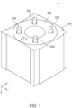
- FIG. 1 is a schematic perspective view illustrating the outer appearance of a magnetic field detection device 1 according to a first embodiment of the present invention.
- the magnetic field detection device 1 is constituted of a cover member 100 and a main body part 200 housed in the cover member 100.
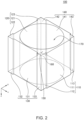
- the cover member 100 has four side surfaces 110, 120, 130, and 140, an upper surface 150, and a lower surface 160, and a housing part 170 is formed so as to penetrate the cover member 100 in the z-direction from the upper surface 150 to the lower surface 160.
- the main body part 200 is housed in the housing part 170 formed in the cover member 100.
- the side surfaces 110 and 120 of the cover member 100 constitute the yz plane and positioned on mutually opposite sides.
- the side surfaces 130 and 140 of the cover member 100 constitute the xz plane and positioned on mutually opposite sides.
- the upper and lower surfaces 150 and 160 of the cover member 100 constitute the xy plane and positioned on mutually opposite sides.
- the side surfaces 110, 120 and the side surfaces 130, 140 are perpendicular to each other.
- the width of each of the side surfaces 110 and 120 in the y-direction is the same as the width of each of the side surfaces 130 and 140 in the x-direction. That is, the outer shape of the cover member 100 is substantially square as viewed in the z-direction.
- the side surface 110 has a first part 111, a second part 112, and a third part 113.
- the first part 111 is sandwiched between the second and third parts 112 and 113 in the y-direction and protrudes in the x-direction from the second and third parts 112 and 113.
- a step formed by the first and second parts 111 and 112 and a step formed by the first and third parts 111 and 113 both extend in the z-direction and constitute an engagement portion of the side surface 110.
- the side surface 120 has a first part 121, a second part 122, and a third part 123.
- the first part 121 is sandwiched between the second and third parts 122 and 123 in the y-direction and is recessed in the x-direction from the second and third parts 122 and 123.
- a step formed by the first and second parts 121 and 122 and a step formed by the first and third parts 121 and 123 both extend in the z-direction and constitute an engagement portion of the side surface 120.
- the engagement portion of the side surface 120 has a shape engageable with the engagement portion of the side surface 110. That is, the width of the first part 121 of the side surface 120 in the y-direction is designed to be substantially equal to or slightly larger than the width of the first part 111 of the side surface 110 in the y-direction.
- the side surface 130 has a first part 131, a second part 132, and a third part 133.
- the first part 131 is sandwiched between the second and third parts 132 and 133 in the x-direction and is recessed in the y-direction from the second and third parts 132 and 133.
- a step formed by the first and second parts 131 and 132 and a step formed by the first and third parts 131 and 133 both extend in the z-direction and constitute an engagement portion of the side surface 130.
- the side surface 140 has a first part 141, a second part 142, and a third part 143.
- the first part 141 is sandwiched between the second and third parts 142 and 143 in the x-direction and protrudes in the y-direction from the second and third parts 142 and 143.
- a step formed by the first and second parts 141 and 142 and a step formed by the first and third parts 141 and 143 both extend in the z-direction and constitute an engagement portion of the side surface 140.
- the engagement portion of the side surface 140 has a shape engageable with the engagement portion of the side surface 130. That is, the width of the first part 141 of the side surface 140 in the x-direction is designed to be substantially equal to or slightly smaller than the width of the first part 131 of the side surface 130 in the x-direction.
- FIGS. 3 and 4 are views illustrating the outer appearance of the main body part 200.
- FIG. 3 is a schematic perspective view as viewed from a measurement surface side
- FIG. 4 is a schematic perspective view as viewed from a back surface side.
- the main body part 200 includes a bobbin 10 made of a resin material, a cancel coil C2 wound around the bobbin 10, and a plurality of magnetic sensors S1 and S21 to S24 fixed to the bobbin 10.
- the bobbin 10 is housed in the housing part 170 of the cover member 100 and fixed therein.
- the cancel coil C2 is covered and protected with the cover member 100 in a direction (radial direction) perpendicular to the axial direction thereof.
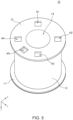
- the bobbin 10 includes a winding core part 13 and flange parts 11 and 12 provided at both ends of the winding core part 13 in the z-direction.
- the outer peripheral surface of the winding core part 13 has a circular shape as viewed in the z-direction.
- the cancel coil C2 is wound around the winding core part 13 of the bobbin 10, and thus the axial direction of the cancel coil C2 is the z-direction.
- the winding core part 13 is formed into a tubular shape and has a hollow part 14 extending in the z-direction.
- the outer peripheral surface of the winding core part 13 may not necessarily have a circular shape and may be a quadrangular shape, an octagonal shape, or an elliptic shape.
- cavities A0 to A4 are formed in the winding core part 13 of the bobbin 10.
- the cavities A0 to A4 are through holes penetrating the winding core part 13 in the z-direction.
- One end of each of the cavities A0 to A4 in the z-direction is opened at the surface of the flange part 11, and the other end thereof in the z-direction is opened at the surface of the flange part 12.
- the radial direction positions of the respective cavities A0 to A4 are the same.
- the magnetic sensor S1 is installed in the cavity A0, and the magnetic sensors S21 to S24 are installed in the cavities A1 to A4, respectively.
- a sensor head of the magnetic sensor S1 protrudes in the z-direction from the flange part 11, and sensor heads of the respective magnetic sensors S21 to S24 protrude in the z-direction from the flange part 12.
- the magnetic sensors S1 and S21 to S24 are connected to a circuit board 15 fixed to the flange part 11 of the bobbin 10.
- the magnetic sensors S1 and S21 to S24 are each disposed at a position overlapping the inner diameter area of the cancel coil C2 as viewed in the z-direction. Further, the position of the sensor head of the magnetic sensor S1 in the z-direction and the positions of the sensor heads of the respective magnetic sensors S21 to S24 in the z-direction differ from each other. The positions of the sensor heads of the respective magnetic sensors S21 to S24 in the z-direction are the same. Further, the radial direction positions of the sensor heads centering around the coil axis are the same among the magnetic sensors S1 and S21 to S24.
- the magnetic sensor S1 is a sensor for detecting an environmental magnetic field component such as terrestrial magnetism, while the magnetic sensors S21 to S24 are sensors for detecting a signal magnetic field component emitted from an object to be measured.
- the sensitivity axis directions of the magnetic sensors S1 and S21 to S24 are all along the z-direction. Although the major part of each of the magnetic sensors S1 and S21 to S24 are positioned in the inner diameter area of the cancel coil C2, the sensor heads of the respective magnetic sensors S21 to S24 protrude from the flange part 12, as described above. Due to this structure, the sensor heads of the magnetic sensors S21 to S24 come closer to an object to be measured.
- the magnetic sensor S1 when the sensor heads of the magnetic sensors S21 to S24 are embedded in the bobbin 10, the distance between an object to be measured and the magnetic sensors S21 to S24 becomes large.
- the sensor head of the magnetic sensor S1 need not protrude from the flange part 11; however, to enhance the symmetry with the magnetic sensors S21 to S24, the magnetic sensor S1 preferably protrudes from the flange part 11 by the amount equal to the protruding amount of the magnetic sensors S21 to S24 from the flange part 12.
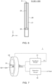
- FIG. 6 is a schematic view illustrating an example of the internal structure of the magnetic sensors S1 and S21 to S24.
- the magnetic sensors S1 and S21 to S24 have the same structure and each include a sensor housing body 20, a substrate 21 housed in the sensor housing body 20, a sensor chip 22, and a magnetism collector 23.
- the sensor chip 22 and magnetism collector 23 are mounted on the substrate 21.
- the magnetism collector 23 has a rod-like shape extending in the z-direction and is made of a high permeability material such as ferrite.
- One end of the magnetism collector 23 in the z-direction constitutes a sensor head H, and the sensor chip 22 is disposed at the other end of the magnetism collector 23 in the z-direction.
- FIG. 7 is a block diagram illustrating the circuit configuration of the main body part 200.
- the main body part 200 includes a feedback circuit 31 connected to the magnetic sensor S1 and a detection circuit 32 connected to the magnetic sensors S21 to S24.
- the feedback circuit 31 is a circuit generating a feedback current F1 for canceling the signal magnetic field component, and the feedback current F1 generated by the feedback circuit 31 is supplied to the cancel coil C2.
- the magnetic sensor S1, feedback circuit 31, and cancel coil C2 constitute a feedback loop for canceling the environmental magnetic field component.
- the detection circuit 32 generates, according to output signals from the magnetic sensors S21 to S24, a detection signal Vout indicating the signal magnetic field component emitted from an object to be measured.
- FIG. 8 is a schematic plan view of the sensor chip 22, and FIG. 9 is a schematic cross-sectional view taken along the line A-A in FIG. 8 .
- the sensor chip 22 has, on its element formation surface, four magnetoresistance effect elements M1 to M4 and a cancel coil C1.
- the cancel coil C1 is covered with an insulating film 24, and the magnetoresistance effect elements M1 to M4 are formed on the insulating film 24.
- the magnetoresistance effect elements M1 to M4 are covered with an insulating film 25.
- the magnetism collector 23 is disposed between the magnetoresistance effect elements M1, M2 and the magnetoresistance effect elements M3, M4 as viewed in the z-direction.
- a magnetic field in the z-direction collected by the magnetism collector 23 is distributed in the positive x-direction and the negative x-direction on the element formation surface of the sensor chip 22.
- magnetic field components in mutually opposite directions are applied to the magnetoresistance effect elements M1, M2 and magnetoresistance effect elements M3, M4.
- the fixed magnetization directions of the magnetoresistance effect elements M1 to M4 are made uniform in the positive x-direction or negative x-direction.
- the cancel coil C1 is disposed so as to overlap the magnetoresistance effect elements M1 to M4.
- cancel magnetic fields in mutually opposite directions are applied to the magnetoresistance effect elements M1, M2 and magnetoresistance effect elements M3, M4.
- FIG. 10 is a circuit diagram of the feedback loop constituted by the magnetic sensor S1, feedback circuit 31, and cancel coil C2.
- the magnetoresistance effect elements M1 to M4 included in the magnetic sensor S1 are bridge-connected, and a differential signal generated thereby is supplied to a differential amplifier 31a included in the feedback circuit 31.
- the differential amplifier 31a generates the feedback current F1 based on the supplied differential signal.
- the feedback current F1 flows in the series-connected cancel coils C1 and C2. This causes the cancel coils C1 and C2 to generate a cancel magnetic field so as to make a differential signal component which is an output signal of the magnetic sensor S1 zero.
- a resistor R1 is connected in parallel to the cancel coil C2.
- the resistance value of the resistor R1 is larger than the equivalent series resistance (ESR) of the cancel coil C2 and is preferably set to 10 times or more, and more preferably, 100 times or more the ESR of the cancel coil C2.
- ESR equivalent series resistance
- FIG. 11 is a circuit diagram of a circuit constituted by the magnetic sensors S21 to S24 and detection circuit 32.
- the magnetoresistance effect elements M1 to M4 included in each of the magnetic sensors S21 to S24 are bridge-connected, and a differential signal generated thereby is supplied to a differential amplifier 32a included in the detection circuit 32.
- the differential amplifier 32a generates a feedback current F2 based on the differentia signal.
- the feedback current F2 flows in the cancel coil C1. This causes the cancel coil C1 to generate a cancel magnetic field so as to make a differential signal component as output signals of the magnetic sensors S21 to S24 zero.
- the detection circuit 32 has a resistor R2 that current-voltage converts the feedback current F2 and a voltage measurement circuit 33 that measures a voltage across the resistor R2.
- a detection signal Vout proportional to the amount of the flowing current is generated.
- FIG. 12 is a schematic view for explaining the positions of the magnetic sensors S1 and S21 to S24 in the radial direction.
- the magnetic sensor S1 is disposed at a position offset from the center of the inner diameter area of the cancel coil C2.
- the cancel coil C2 generates a cancel magnetic field so as to make the environmental magnetic field component to be applied to the magnetic sensor S1 zero.
- the environmental magnetic field component becomes zero not only at the position where the magnetic sensor S1 is disposed but also in a cancel space 40 distributed concentrically with the cancel coil C2. This is because that the intensity distribution of the cancel magnetic field spreads concentrically, so that when the environmental magnetic field component is uniform, it is completely cancelled in the area lying in the same radial position as the magnetic sensor S1.
- the cancel space 40 is present on the flange part 11 side where the sensor head of the magnetic sensor S1 is positioned and symmetrically on the flange part 12 side where the sensor heads of the magnetic sensors S21 to S24 are positioned.
- the magnetic sensors S21 to S24 are disposed in the cancel space 40 on the flange part 12 side.
- the environmental magnetic field component to be applied to the magnetic sensors S21 to S24 also becomes zero, with the result that only the signal magnetic field component emitted from an object to be measured is applied to the magnetic sensors S21 to S24.
- the cancel coil C2 is assigned in common to the five magnetic sensors S1 and S21 to S24, so that it is possible to reduce the number of components and to simplify the circuit configuration.
- the cavities A0 to A4 are disposed at the same radial position, so that the environmental magnetic field component to be applied to the magnetic sensors S21 to S24 becomes zero.
- the sensor head of the magnetic sensor S1 for detecting the environmental magnetic field component is provided on the flange part 11 side, and the sensor heads of the respective magnetic sensors S21 to S24 for detecting the signal magnetic field component are provided on the flange part 12 side, so that the signal magnetic field component emitted from an object to be measured is hardly applied to the magnetic sensor S1. This prevents a part or all of the signal magnetic field components from being cancelled.
- the signal magnetic field component emitted from the object to be measured can be detected in real time. Further, since the cancel coil C2 and magnetic sensors S1 and S21 to S24 are fixed to the same bobbin 10, displacement between the cancel coil C2 and the magnetic sensors S1 and S21 to S24 hardly occurs.
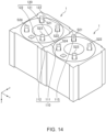
- FIG. 14 is a schematic perspective view illustrating a magnetic field detection device array obtained by combining two magnetic field detection devices 1.
- the side surface 110 of one magnetic field detection device 1 and the side surface 120 of the other magnetic field detection device 1 are made to face each other, and the engagement portions thereof are engaged. That is, the first to third parts 111 to 113 of the side surface 110 are respectively in close contact with the first to third parts 121 to 123 of the side surface 120, whereby the y-direction position of the two magnetic field detection devices 1 is fixed.
- the side surface 130 of one magnetic field detection device 1 and the side surface 140 of the other magnetic field detection device 1 are made to face each other, and the engagement portions thereof are engaged, whereby the x-direction position of the two magnetic field detection devices 1 is fixed.
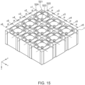
- FIG. 15 is a schematic perspective view illustrating a magnetic field detection device array obtained by combining nine magnetic field detection devices 1.
- nine magnetic field detection devices 1 are connected in a 3 x 3 array.
- the engagement portions formed respectively in the side surfaces 110 and 120 of the two magnetic field detection devices 1 adjacent to each other in the x-direction are engaged with each other
- the engagement portions formed respectively in the side surfaces 130 and 140 of the two magnetic field detection devices 1 adjacent to each other in the y-direction are engaged with each other.
- the magnetic sensors S21 to S24 for detecting the signal magnetic field component can be arranged in a matrix in the xy plane.
- the magnetic sensor S21, S22, S23 or S24 is disposed at each of the intersections between virtual lines x1 to x6 extending in the x-direction and virtual lines y1 to y6 extending in the y-direction.
- the magnetic sensor S1 for detecting the environmental magnetic field component need not be provided in all the magnetic field detection devices 1, but it may be provided only in one of the magnetic field detection devices 1 and, in this case, the feedback current F1 may be supplied to the cancel coil C2 of each of the plurality of magnetic field detection devices 1. This can reduce the number of magnetic sensors to be used.
- the plurality of magnetic field detection devices 1 can be desirably combined.
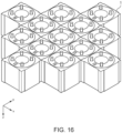
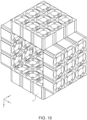
- combination modes illustrated in FIGS. 16 to 19 are possible.
- FIG. 16 is an example in which the number of the magnetic field detection devices 1 differs depending on the position in the x-direction and the position in the y-direction.
- FIG. 17 is an example in which the position of the magnetic field detection device 1 in the z-direction differs depending on the position in the x-direction and the position in the y-direction.
- FIG. 18 is an example in which 12 magnetic field detection devices 1 are arranged in a ring shape
- FIG. 19 is an example in which three rings each including 12 magnetic field detection devices 1 are combined.
- the side surfaces 110, 120, 130, and 140 of the cover member 100 housing the main body part 200 each have the engagement portion, so that it is possible to arrange a desired number of the magnetic field detection devices 1 in the respective x- and y- directions without displacement. This makes it possible to easily change the number and layout of the magnetic field detection devices 1.
- FIG. 20 is a schematic perspective view illustrating a magnetic field detection device array obtained by combining four magnetic field detection devices 2 according to a second embodiment of the present invention.
- the magnetic field detection device 2 according to the second embodiment differs from the magnetic field detection device 1 according to the first embodiment in that the width of the side surfaces 130 and 140 in the x-direction is larger than the width of the side surfaces 110 and 120 in the y-direction. That is, in the present embodiment, the cover member 100 has a substantially rectangular outer shape as viewed in the z-direction. As exemplified by the magnetic field detection device 2 according to the second embodiment, the outer shape of the cover member 100 as viewed in the z-direction is not limited to a square in the present invention.
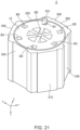
- FIG. 21 is a schematic perspective view illustrating the outer shape of a magnetic field detection device 3 according to a third embodiment of the present invention.
- the magnetic field detection device 3 differs from the magnetic field detection device 1 according to the first embodiment in that a cover member 300 has a hexagonal outer shape as viewed in the z-direction.
- the cover member 300 has six side surfaces 310, 320, 330, 340, 350, and 360.
- the side surfaces 310 and 320 are perpendicular to the direction a
- the side surfaces 330 and 340 are perpendicular to the direction b
- the side surfaces 350 and 360 are perpendicular to the direction c.
- the directions a, b, and c form an angle of 60° or 120° with one another.
- the side surface 310 (320), side surface 330 (340), and side surface 350 (360) form 60° or 120° with one another.
- the engagement portion formed in the side surface 310 and the engagement portion formed in the side surface 320 positioned on the side opposite the side surface 310 have shapes engageable with each other
- the engagement portion formed in the side surface 330 and the engagement portion formed in the side surface 340 positioned on the side opposite the side surface 330 have shapes engageable with each other
- the engagement portion formed in the side surface 350 and the engagement portion formed in the side surface 360 positioned on the side opposite the side surface 350 have shapes engageable with each other.
- a cavity B0 is formed at the center portion of the bobbin 10
- six cavities B1 to B6 are concentrically formed around the cavity B0.
- the magnetic sensor S21 for detecting the signal magnetic field component is inserted into the cavity B1.
- the magnetic sensors S22 to S24 for detecting the signal magnetic field component or the magnetic sensor S1 for detecting the environmental magnetic field component may be inserted into the remaining cavities B2 to B6.
- the magnetic sensor S1 When the magnetic sensor S1 is inserted into the cavity B0, it is necessary to adjust the gain of the feedback loop so as to completely cancel the environmental magnetic field component not at the position where the magnetic sensor S1 itself is provided but at the position where the magnetic sensor S21 is provided.
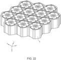
- FIG. 22 is a schematic perspective view illustrating a magnetic field detection device array obtained by combining 14 magnetic field detection devices 3.
- the engagement portions formed in the side surfaces 310 and 320 of the magnetic field detection device 3 adjacent in the direction a are engaged with each other
- the engagement portions formed in the side surfaces 330 and 340 of the magnetic field detection device 3 adjacent in the direction b are engaged with each other
- the engagement portions formed in the side surfaces 350 and 360 of the magnetic field detection device 3 adjacent in the direction c are engaged with each other.
- a plurality of the magnetic field detection devices 3 can be arranged in a honeycomb pattern.
- the magnetic sensors are fixed to the bobbin in the above embodiments, they may be fixed to the cover member having cavities.
- the engagement portion is constituted by steps extending in the z-direction
- the shape of the engagement portion is not limited to this.
- the widths of the first part 111 of the side surface 110 and first part 121 of the side surface 120 in the y-direction may each be made to differ depending on the z-direction position so as to fix the two magnetic field detection devices to be engaged in not only the y-direction but also the z-direction.
- the side surface 110 of one magnetic field detection device and the side surface 120 of the other magnetic field detection device may be engaged with screws.
- the number of the magnetic sensors for detecting the environmental magnetic field component is not particularly limited to a specific number.
Landscapes
- Physics & Mathematics (AREA)
- Condensed Matter Physics & Semiconductors (AREA)
- General Physics & Mathematics (AREA)
- Measuring Magnetic Variables (AREA)
- Hall/Mr Elements (AREA)
Abstract
Description
- The present invention relates to a magnetic field detection device and, more particularly, to a magnetic field detection devices capable of being arranged in an array.
-
Patent Document 1 discloses inFIG. 12 a magnetic field detection device array that can measure in-plane magnetic field distribution by arranging a plurality of magnetic field detection devices in an array. - [Patent Document 1]
JP 2017-133993A - However, in the magnetic field detection device array disclosed in
FIG. 12 ofPatent Document 1, it is not easy to change the number and layout of the magnetic field detection devices. - It is therefore an object of the present invention to facilitate a change in the number and layout of the magnetic field detection devices to be arranged in an array.
- A magnetic field detection device according to the present invention includes: a bobbin; a cancel coil wound around the bobbin; a cover member fixed to the bobbin and covering the cancel coil in a direction perpendicular to the axial direction of the cancel coil; and a first magnetic sensor fixed to the bobbin or cover member. The cover member has first and second side surfaces extending in the axial direction of the cancel coil and positioned on mutually opposite sides. The first and second side surfaces have first and second engagement portions, respectively. The first engagement portion has a shape engageable with the shape of the second engagement portion.
- According to the present invention, the cover member covering the cancel coil in a direction perpendicular to the axial direction has the first and second engagement positions, so that it is possible to arrange a desired number of the magnetic field detection devices in a first direction perpendicular to the first and second side surfaces.
- In the present invention, the cover member may have third and fourth side surfaces extending in the axial direction of the cancel coil and positioned on mutually opposite sides, the third and fourth side surfaces may have third and fourth engagement portions, respectively, and the third engagement portion may have a shape engageable with the shape of the fourth engagement portion. This makes it possible to arrange a desired number of the magnetic field detection devices in a second direction perpendicular to the third and fourth side surfaces. In this case, the first and second side surfaces may be perpendicular to the third and fourth side surfaces. With this configuration, by engaging the first and second engagement portions of two magnetic field detection devices adjacent to each other in the first direction and engaging the third and fourth engagement portions of two magnetic field detection devices adjacent to each other in the second direction, it is possible to constitute a magnetic field detection device array in which a plurality of the magnetic field detection devices are arranged in a matrix.
- In the present invention, the cover member may have fifth and sixth side surfaces extending in the axial direction of the cancel coil and positioned on mutually opposite sides, the fifth and sixth side surfaces may have fifth and sixth engagement portions, respectively, the fifth engagement portion may have a shape engageable with the shape of the sixth engagement portion, and the first and second side surfaces, the third and fourth side surface, and the fifth and sixth side surfaces may form an angle of 60° with one another. With this configuration, by engaging the first and second engagement portions of two magnetic field detection devices adjacent to each other in the first direction, engaging the third and fourth engagement portions of two magnetic field detection devices adjacent to each other in the second direction, and engaging the fifth and sixth engagement portions of two magnetic field detection devices adjacent to each other in a third direction, it is possible to constitute a magnetic field detection device array in which a plurality of the magnetic field detection devices are arranged in a honeycomb pattern.
- The magnetic field detection device according to the present invention may further include a second magnetic sensor fixed to the bobbin or cover member and a feedback circuit that makes a cancel current flow in the cancel coil according to an output signal of the second magnetic sensor to cancel an environmental magnetic field in a cancel space, and the first magnetic sensor may be disposed in the cancel space. This makes it possible to cancel a uniform environmental magnetic field component such as terrestrial magnetism. In addition, the cancel coil is used in common for the first and second magnetic sensors, so that it is possible to reduce the number of components to be used and to simplify the circuit configuration.
- In the present invention, sensor heads of the first and second magnetic sensors may be different in position in the axial direction of the cancel coil. This makes it possible to prevent a signal magnetic field component from being cancelled by the cancel coil. In this case, a winding core part of the bobbin may have a first cavity opened at one side thereof in the axial direction and a second cavity opened at the other side thereof in the axial direction, and the first and second magnetic sensors may be installed in the first and second cavities, respectively. This makes it possible to sufficiently separate the first and second magnetic sensors from each other. Further, in this case, the sensor head of the first magnetic sensor may protrude from the bobbin or cover member toward one side in the axial direction, and the sensor head of the second magnetic sensor may protrude from the bobbin or cover member toward the other side in the axial direction. This makes it possible to bring an object to be measured close to the first magnetic sensor.
- According to the present invention, it is possible to facilitate a change in the number and layout of the magnetic field detection devices to be arranged in an array.
-
-
FIG. 1 is a schematic perspective view illustrating the outer appearance of a magneticfield detection device 1 according to a first embodiment of the present invention. -
FIG. 2 is a schematic perspective view illustrating the outer appearance of acover member 100. -
FIG. 3 is a schematic perspective view illustrating amain body part 200 as viewed from a measurement surface side. -
FIG. 4 is a schematic perspective view illustrating themain body part 200 as viewed from a back surface side. -
FIG. 5 is a schematic perspective view illustrating the outer appearance of abobbin 10. -
FIG. 6 is a schematic view illustrating an example of the internal structure of the magnetic sensors S1 and S21 to S24. -
FIG. 7 is a block diagram illustrating the circuit configuration of themain body part 200. -
FIG. 8 is a schematic plan view of thesensor chip 22. -
FIG. 9 is a schematic cross-sectional view taken along the line A-A inFIG. 8 . -
FIG. 10 is a circuit diagram of the feedback loop constituted by the magnetic sensor S1,feedback circuit 31, and cancel coil C2. -
FIG. 11 is a circuit diagram of a circuit constituted by the magnetic sensors S21 to S24 anddetection circuit 32. -
FIG. 12 is a schematic view for explaining the positions of the magnetic sensors S1 and S21 to S24 in the radial direction. -
FIG. 13 is a schematic view for explaining the position of acancel space 40. -
FIG. 14 is a schematic perspective view illustrating a magnetic field detection device array obtained by combining two magneticfield detection devices 1. -
FIG. 15 is a schematic perspective view illustrating a magnetic field detection device array obtained by combining nine magneticfield detection devices 1. -
FIG. 16 is a schematic perspective view illustrating a magnetic field detection device array according to a first modification. -
FIG. 17 is a schematic perspective view illustrating a magnetic field detection device array according to a second modification. -
FIG. 18 is a schematic perspective view illustrating a magnetic field detection device array according to a third modification. -
FIG. 19 is a schematic perspective view illustrating a magnetic field detection device array according to a fourth modification. -
FIG. 20 is a schematic perspective view illustrating a magnetic field detection device array obtained by combining four magneticfield detection devices 2 according to a second embodiment of the present invention. -
FIG. 21 is a schematic perspective view illustrating the outer shape of a magneticfield detection device 3 according to a third embodiment of the present invention. -
FIG. 22 is a schematic perspective view illustrating a magnetic field detection device array obtained by combining 14 magneticfield detection devices 3. - Hereinafter, preferred embodiments of the present invention will be described in detail with reference to the accompanying drawings.
-
FIG. 1 is a schematic perspective view illustrating the outer appearance of a magneticfield detection device 1 according to a first embodiment of the present invention. - As illustrated in
FIG. 1 , the magneticfield detection device 1 according to the first embodiment is constituted of acover member 100 and amain body part 200 housed in thecover member 100. As illustrated inFIG. 2 , thecover member 100 has fourside surfaces upper surface 150, and alower surface 160, and ahousing part 170 is formed so as to penetrate thecover member 100 in the z-direction from theupper surface 150 to thelower surface 160. Themain body part 200 is housed in thehousing part 170 formed in thecover member 100. Theside surfaces cover member 100 constitute the yz plane and positioned on mutually opposite sides. Theside surfaces cover member 100 constitute the xz plane and positioned on mutually opposite sides. The upper andlower surfaces cover member 100 constitute the xy plane and positioned on mutually opposite sides. Theside surfaces side surfaces cover member 100 is substantially square as viewed in the z-direction. - The
side surface 110 has afirst part 111, asecond part 112, and athird part 113. Thefirst part 111 is sandwiched between the second andthird parts third parts second parts third parts side surface 110. - The
side surface 120 has afirst part 121, asecond part 122, and athird part 123. Thefirst part 121 is sandwiched between the second andthird parts third parts second parts third parts side surface 120. The engagement portion of theside surface 120 has a shape engageable with the engagement portion of theside surface 110. That is, the width of thefirst part 121 of theside surface 120 in the y-direction is designed to be substantially equal to or slightly larger than the width of thefirst part 111 of theside surface 110 in the y-direction. - The
side surface 130 has afirst part 131, asecond part 132, and athird part 133. Thefirst part 131 is sandwiched between the second andthird parts third parts second parts third parts side surface 130. - The
side surface 140 has afirst part 141, asecond part 142, and athird part 143. Thefirst part 141 is sandwiched between the second andthird parts third parts second parts third parts side surface 140. The engagement portion of theside surface 140 has a shape engageable with the engagement portion of theside surface 130. That is, the width of thefirst part 141 of theside surface 140 in the x-direction is designed to be substantially equal to or slightly smaller than the width of thefirst part 131 of theside surface 130 in the x-direction. -
FIGS. 3 and4 are views illustrating the outer appearance of themain body part 200.FIG. 3 is a schematic perspective view as viewed from a measurement surface side, andFIG. 4 is a schematic perspective view as viewed from a back surface side. - As illustrated in
FIGS. 3 and4 , themain body part 200 includes abobbin 10 made of a resin material, a cancel coil C2 wound around thebobbin 10, and a plurality of magnetic sensors S1 and S21 to S24 fixed to thebobbin 10. Thebobbin 10 is housed in thehousing part 170 of thecover member 100 and fixed therein. As a result, the cancel coil C2 is covered and protected with thecover member 100 in a direction (radial direction) perpendicular to the axial direction thereof. As illustrated inFIG. 5 , thebobbin 10 includes a windingcore part 13 andflange parts core part 13 in the z-direction. The outer peripheral surface of the windingcore part 13 has a circular shape as viewed in the z-direction. The cancel coil C2 is wound around the windingcore part 13 of thebobbin 10, and thus the axial direction of the cancel coil C2 is the z-direction. The windingcore part 13 is formed into a tubular shape and has ahollow part 14 extending in the z-direction. The outer peripheral surface of the windingcore part 13 may not necessarily have a circular shape and may be a quadrangular shape, an octagonal shape, or an elliptic shape. - In the present embodiment, five cavities A0 to A4 are formed in the winding
core part 13 of thebobbin 10. The cavities A0 to A4 are through holes penetrating the windingcore part 13 in the z-direction. One end of each of the cavities A0 to A4 in the z-direction is opened at the surface of theflange part 11, and the other end thereof in the z-direction is opened at the surface of theflange part 12. The radial direction positions of the respective cavities A0 to A4 are the same. In the present embodiment, the magnetic sensor S1 is installed in the cavity A0, and the magnetic sensors S21 to S24 are installed in the cavities A1 to A4, respectively. A sensor head of the magnetic sensor S1 protrudes in the z-direction from theflange part 11, and sensor heads of the respective magnetic sensors S21 to S24 protrude in the z-direction from theflange part 12. The magnetic sensors S1 and S21 to S24 are connected to acircuit board 15 fixed to theflange part 11 of thebobbin 10. - With the above configuration, the magnetic sensors S1 and S21 to S24 are each disposed at a position overlapping the inner diameter area of the cancel coil C2 as viewed in the z-direction. Further, the position of the sensor head of the magnetic sensor S1 in the z-direction and the positions of the sensor heads of the respective magnetic sensors S21 to S24 in the z-direction differ from each other. The positions of the sensor heads of the respective magnetic sensors S21 to S24 in the z-direction are the same. Further, the radial direction positions of the sensor heads centering around the coil axis are the same among the magnetic sensors S1 and S21 to S24.
- The magnetic sensor S1 is a sensor for detecting an environmental magnetic field component such as terrestrial magnetism, while the magnetic sensors S21 to S24 are sensors for detecting a signal magnetic field component emitted from an object to be measured. The sensitivity axis directions of the magnetic sensors S1 and S21 to S24 are all along the z-direction. Although the major part of each of the magnetic sensors S1 and S21 to S24 are positioned in the inner diameter area of the cancel coil C2, the sensor heads of the respective magnetic sensors S21 to S24 protrude from the
flange part 12, as described above. Due to this structure, the sensor heads of the magnetic sensors S21 to S24 come closer to an object to be measured. That is, when the sensor heads of the magnetic sensors S21 to S24 are embedded in thebobbin 10, the distance between an object to be measured and the magnetic sensors S21 to S24 becomes large. On the other hand, the sensor head of the magnetic sensor S1 need not protrude from theflange part 11; however, to enhance the symmetry with the magnetic sensors S21 to S24, the magnetic sensor S1 preferably protrudes from theflange part 11 by the amount equal to the protruding amount of the magnetic sensors S21 to S24 from theflange part 12. -
FIG. 6 is a schematic view illustrating an example of the internal structure of the magnetic sensors S1 and S21 to S24. - In the example illustrated in
FIG. 6 , the magnetic sensors S1 and S21 to S24 have the same structure and each include asensor housing body 20, asubstrate 21 housed in thesensor housing body 20, asensor chip 22, and amagnetism collector 23. Thesensor chip 22 andmagnetism collector 23 are mounted on thesubstrate 21. Themagnetism collector 23 has a rod-like shape extending in the z-direction and is made of a high permeability material such as ferrite. One end of themagnetism collector 23 in the z-direction constitutes a sensor head H, and thesensor chip 22 is disposed at the other end of themagnetism collector 23 in the z-direction. With this configuration, the signal magnetic field component in the z-direction emitted from an object to be measured positioned in the vicinity of the sensor head H is collected by themagnetism collector 23 so as to be applied to thesensor chip 22. -
FIG. 7 is a block diagram illustrating the circuit configuration of themain body part 200. - As illustrated in
FIG. 7 , themain body part 200 includes afeedback circuit 31 connected to the magnetic sensor S1 and adetection circuit 32 connected to the magnetic sensors S21 to S24. Thefeedback circuit 31 is a circuit generating a feedback current F1 for canceling the signal magnetic field component, and the feedback current F1 generated by thefeedback circuit 31 is supplied to the cancel coil C2. As a result, the magnetic sensor S1,feedback circuit 31, and cancel coil C2 constitute a feedback loop for canceling the environmental magnetic field component. On the other hand, thedetection circuit 32 generates, according to output signals from the magnetic sensors S21 to S24, a detection signal Vout indicating the signal magnetic field component emitted from an object to be measured. -
FIG. 8 is a schematic plan view of thesensor chip 22, andFIG. 9 is a schematic cross-sectional view taken along the line A-A inFIG. 8 . - As illustrated in
FIGS. 8 and 9 , thesensor chip 22 has, on its element formation surface, four magnetoresistance effect elements M1 to M4 and a cancel coil C1. The cancel coil C1 is covered with an insulatingfilm 24, and the magnetoresistance effect elements M1 to M4 are formed on the insulatingfilm 24. The magnetoresistance effect elements M1 to M4 are covered with an insulatingfilm 25. Themagnetism collector 23 is disposed between the magnetoresistance effect elements M1, M2 and the magnetoresistance effect elements M3, M4 as viewed in the z-direction. With this configuration, a magnetic field in the z-direction collected by themagnetism collector 23 is distributed in the positive x-direction and the negative x-direction on the element formation surface of thesensor chip 22. As a result, magnetic field components in mutually opposite directions are applied to the magnetoresistance effect elements M1, M2 and magnetoresistance effect elements M3, M4. The fixed magnetization directions of the magnetoresistance effect elements M1 to M4 are made uniform in the positive x-direction or negative x-direction. - The cancel coil C1 is disposed so as to overlap the magnetoresistance effect elements M1 to M4. When a cancel current is made to flow in the cancel coil C1, cancel magnetic fields in mutually opposite directions are applied to the magnetoresistance effect elements M1, M2 and magnetoresistance effect elements M3, M4.
-
FIG. 10 is a circuit diagram of the feedback loop constituted by the magnetic sensor S1,feedback circuit 31, and cancel coil C2. - As illustrated in
FIG. 10 , the magnetoresistance effect elements M1 to M4 included in the magnetic sensor S1 are bridge-connected, and a differential signal generated thereby is supplied to adifferential amplifier 31a included in thefeedback circuit 31. Thedifferential amplifier 31a generates the feedback current F1 based on the supplied differential signal. The feedback current F1 flows in the series-connected cancel coils C1 and C2. This causes the cancel coils C1 and C2 to generate a cancel magnetic field so as to make a differential signal component which is an output signal of the magnetic sensor S1 zero. - In the present embodiment, a resistor R1 is connected in parallel to the cancel coil C2. The resistance value of the resistor R1 is larger than the equivalent series resistance (ESR) of the cancel coil C2 and is preferably set to 10 times or more, and more preferably, 100 times or more the ESR of the cancel coil C2. Thus, of the feedback current F1, a lower frequency component due to terrestrial magnetism flows in the cancel coil C2, while a high frequency component that is a cause of oscillation is detoured to the resistor R1. This makes it possible to properly cancel the environmental magnetic field component such as terrestrial magnetism while preventing oscillation of the feedback loop.
-
FIG. 11 is a circuit diagram of a circuit constituted by the magnetic sensors S21 to S24 anddetection circuit 32. - As illustrated in
FIG. 9 , the magnetoresistance effect elements M1 to M4 included in each of the magnetic sensors S21 to S24 are bridge-connected, and a differential signal generated thereby is supplied to adifferential amplifier 32a included in thedetection circuit 32. Thedifferential amplifier 32a generates a feedback current F2 based on the differentia signal. The feedback current F2 flows in the cancel coil C1. This causes the cancel coil C1 to generate a cancel magnetic field so as to make a differential signal component as output signals of the magnetic sensors S21 to S24 zero. - Further, the
detection circuit 32 has a resistor R2 that current-voltage converts the feedback current F2 and avoltage measurement circuit 33 that measures a voltage across the resistor R2. Thus, when the feedback current F2 flows, a detection signal Vout proportional to the amount of the flowing current is generated. -
FIG. 12 is a schematic view for explaining the positions of the magnetic sensors S1 and S21 to S24 in the radial direction. - As illustrated in
FIG. 12 , as viewed in the axial direction (z-direction) of the cancel coil C2, the magnetic sensor S1 is disposed at a position offset from the center of the inner diameter area of the cancel coil C2. As described above, the cancel coil C2 generates a cancel magnetic field so as to make the environmental magnetic field component to be applied to the magnetic sensor S1 zero. However, the environmental magnetic field component becomes zero not only at the position where the magnetic sensor S1 is disposed but also in a cancelspace 40 distributed concentrically with the cancel coil C2. This is because that the intensity distribution of the cancel magnetic field spreads concentrically, so that when the environmental magnetic field component is uniform, it is completely cancelled in the area lying in the same radial position as the magnetic sensor S1. - As illustrated in
FIG. 13 , the cancelspace 40 is present on theflange part 11 side where the sensor head of the magnetic sensor S1 is positioned and symmetrically on theflange part 12 side where the sensor heads of the magnetic sensors S21 to S24 are positioned. In the present embodiment, the magnetic sensors S21 to S24 are disposed in the cancelspace 40 on theflange part 12 side. Thus, the environmental magnetic field component to be applied to the magnetic sensors S21 to S24 also becomes zero, with the result that only the signal magnetic field component emitted from an object to be measured is applied to the magnetic sensors S21 to S24. This makes it possible to detect even a weak magnetic field without using a shield room. In addition, the cancel coil C2 is assigned in common to the five magnetic sensors S1 and S21 to S24, so that it is possible to reduce the number of components and to simplify the circuit configuration. - In the present embodiment, the cavities A0 to A4 are disposed at the same radial position, so that the environmental magnetic field component to be applied to the magnetic sensors S21 to S24 becomes zero. In addition, in the present embodiment, the sensor head of the magnetic sensor S1 for detecting the environmental magnetic field component is provided on the
flange part 11 side, and the sensor heads of the respective magnetic sensors S21 to S24 for detecting the signal magnetic field component are provided on theflange part 12 side, so that the signal magnetic field component emitted from an object to be measured is hardly applied to the magnetic sensor S1. This prevents a part or all of the signal magnetic field components from being cancelled. Thus, when measurement is performed with an object to be measured that generates a weak magnetic field brought close to the sensor heads of the magnetic sensors S21 to S24, the signal magnetic field component emitted from the object to be measured can be detected in real time. Further, since the cancel coil C2 and magnetic sensors S1 and S21 to S24 are fixed to thesame bobbin 10, displacement between the cancel coil C2 and the magnetic sensors S1 and S21 to S24 hardly occurs. -
FIG. 14 is a schematic perspective view illustrating a magnetic field detection device array obtained by combining two magneticfield detection devices 1. - As illustrated in
FIG. 14 , when the two magneticfield detection devices 1 are connected in the x-direction, theside surface 110 of one magneticfield detection device 1 and theside surface 120 of the other magneticfield detection device 1 are made to face each other, and the engagement portions thereof are engaged. That is, the first tothird parts 111 to 113 of theside surface 110 are respectively in close contact with the first tothird parts 121 to 123 of theside surface 120, whereby the y-direction position of the two magneticfield detection devices 1 is fixed. Although not illustrated, when the two magneticfield detection devices 1 are connected in the y-direction, theside surface 130 of one magneticfield detection device 1 and theside surface 140 of the other magneticfield detection device 1 are made to face each other, and the engagement portions thereof are engaged, whereby the x-direction position of the two magneticfield detection devices 1 is fixed. -
FIG. 15 is a schematic perspective view illustrating a magnetic field detection device array obtained by combining nine magneticfield detection devices 1. - In the example illustrated in
FIG. 15 , nine magneticfield detection devices 1 are connected in a 3 x 3 array. In this case, the engagement portions formed respectively in the side surfaces 110 and 120 of the two magneticfield detection devices 1 adjacent to each other in the x-direction are engaged with each other, and the engagement portions formed respectively in the side surfaces 130 and 140 of the two magneticfield detection devices 1 adjacent to each other in the y-direction are engaged with each other. - When a plurality of the magnetic
field detection devices 1 are arranged in an array in the above manner, the magnetic sensors S21 to S24 for detecting the signal magnetic field component can be arranged in a matrix in the xy plane. In the example illustrated inFIG. 15 , the magnetic sensor S21, S22, S23 or S24 is disposed at each of the intersections between virtual lines x1 to x6 extending in the x-direction and virtual lines y1 to y6 extending in the y-direction. By designing a pitch P between the virtual lines x1 to x6 and a pitch P between the virtual lines y1 to y6 equal to each other, the spatial distribution of the signal magnetic field component can be measured over a wide range. - When a plurality of the magnetic
field detection devices 1 are arranged in an array, the magnetic sensor S1 for detecting the environmental magnetic field component need not be provided in all the magneticfield detection devices 1, but it may be provided only in one of the magneticfield detection devices 1 and, in this case, the feedback current F1 may be supplied to the cancel coil C2 of each of the plurality of magneticfield detection devices 1. This can reduce the number of magnetic sensors to be used. - The plurality of magnetic
field detection devices 1 can be desirably combined. For example, combination modes illustrated inFIGS. 16 to 19 are possible.FIG. 16 is an example in which the number of the magneticfield detection devices 1 differs depending on the position in the x-direction and the position in the y-direction.FIG. 17 is an example in which the position of the magneticfield detection device 1 in the z-direction differs depending on the position in the x-direction and the position in the y-direction.FIG. 18 is an example in which 12 magneticfield detection devices 1 are arranged in a ring shape, andFIG. 19 is an example in which three rings each including 12 magneticfield detection devices 1 are combined. - As described above, in the magnetic
field detection device 1 according to the present embodiment, the side surfaces 110, 120, 130, and 140 of thecover member 100 housing themain body part 200 each have the engagement portion, so that it is possible to arrange a desired number of the magneticfield detection devices 1 in the respective x- and y- directions without displacement. This makes it possible to easily change the number and layout of the magneticfield detection devices 1. -
FIG. 20 is a schematic perspective view illustrating a magnetic field detection device array obtained by combining four magneticfield detection devices 2 according to a second embodiment of the present invention. - As illustrated in
FIG. 20 , the magneticfield detection device 2 according to the second embodiment differs from the magneticfield detection device 1 according to the first embodiment in that the width of the side surfaces 130 and 140 in the x-direction is larger than the width of the side surfaces 110 and 120 in the y-direction. That is, in the present embodiment, thecover member 100 has a substantially rectangular outer shape as viewed in the z-direction. As exemplified by the magneticfield detection device 2 according to the second embodiment, the outer shape of thecover member 100 as viewed in the z-direction is not limited to a square in the present invention. -
FIG. 21 is a schematic perspective view illustrating the outer shape of a magneticfield detection device 3 according to a third embodiment of the present invention. - As illustrated in
FIG. 21 , the magneticfield detection device 3 according to the third embodiment differs from the magneticfield detection device 1 according to the first embodiment in that acover member 300 has a hexagonal outer shape as viewed in the z-direction. In the present embodiment, thecover member 300 has sixside surfaces - Further, the engagement portion formed in the
side surface 310 and the engagement portion formed in theside surface 320 positioned on the side opposite theside surface 310 have shapes engageable with each other, the engagement portion formed in theside surface 330 and the engagement portion formed in theside surface 340 positioned on the side opposite theside surface 330 have shapes engageable with each other, and the engagement portion formed in theside surface 350 and the engagement portion formed in theside surface 360 positioned on the side opposite theside surface 350 have shapes engageable with each other. In the example illustrated inFIG. 21 , a cavity B0 is formed at the center portion of thebobbin 10, and six cavities B1 to B6 are concentrically formed around the cavity B0. The magnetic sensor S21 for detecting the signal magnetic field component is inserted into the cavity B1. The magnetic sensors S22 to S24 for detecting the signal magnetic field component or the magnetic sensor S1 for detecting the environmental magnetic field component may be inserted into the remaining cavities B2 to B6. When the magnetic sensor S1 is inserted into the cavity B0, it is necessary to adjust the gain of the feedback loop so as to completely cancel the environmental magnetic field component not at the position where the magnetic sensor S1 itself is provided but at the position where the magnetic sensor S21 is provided. -
FIG. 22 is a schematic perspective view illustrating a magnetic field detection device array obtained by combining 14 magneticfield detection devices 3. In the example illustrated inFIG. 22 , the engagement portions formed in the side surfaces 310 and 320 of the magneticfield detection device 3 adjacent in the direction a are engaged with each other, the engagement portions formed in the side surfaces 330 and 340 of the magneticfield detection device 3 adjacent in the direction b are engaged with each other, and the engagement portions formed in the side surfaces 350 and 360 of the magneticfield detection device 3 adjacent in the direction c are engaged with each other. As illustrated inFIG. 22 , according to the third embodiment, a plurality of the magneticfield detection devices 3 can be arranged in a honeycomb pattern. - While the preferred embodiment of the present invention has been described, the present invention is not limited to the above embodiment, and various modifications may be made within the scope of the present invention, and all such modifications are included in the present invention.
- For example, although the magnetic sensors are fixed to the bobbin in the above embodiments, they may be fixed to the cover member having cavities.
- Further, although the engagement portion is constituted by steps extending in the z-direction, the shape of the engagement portion is not limited to this. For example, the widths of the
first part 111 of theside surface 110 andfirst part 121 of theside surface 120 in the y-direction may each be made to differ depending on the z-direction position so as to fix the two magnetic field detection devices to be engaged in not only the y-direction but also the z-direction. Further, theside surface 110 of one magnetic field detection device and theside surface 120 of the other magnetic field detection device may be engaged with screws. - Further, although four magnetic sensors for detecting the environmental magnetic field component are provided in the magnetic
field detection device 1 according to the first embodiment, the number of the magnetic sensors for detecting the environmental magnetic field component is not particularly limited to a specific number. -
- 1-3
- magnetic field detection device
- 10
- bobbin
- 11, 12
- flange part
- 13
- winding core part
- 14
- hollow part
- 15
- circuit board
- 20
- sensor housing body
- 21
- substrate
- 22
- sensor chip
- 23
- magnetism collector
- 24, 25
- insulating film
- 31
- feedback circuit
- 31a
- differential amplifier
- 32
- detection circuit
- 32a
- differential amplifier
- 33
- voltage measurement circuit
- 40
- cancel space
- 100
- cover member
- 110, 120, 130, 140
- side surface
- 111, 121, 131, 141
- first part
- 112, 122, 132, 142
- second part
- 113, 123, 133, 143
- third part
- 120
- side surface
- 121
- first part
- 122
- second part
- 150
- upper surface
- 160
- lower surface
- 170
- housing part
- 200
- main body part
- 300
- cover member
- 310, 320, 330, 340, 350, 360
- side surface
- A0-A4, B0-B6
- cavity
- C1, C2
- cancel coil
- F1, F2
- feedback current
- H
- sensor head
- L0-L4
- wiring
- M1-M4
- magnetoresistance effect element
- R1, R2
- resistor
- S1, S21-S24
- magnetic sensor
Claims (10)
- A magnetic field detection device comprising:a bobbin;a cancel coil wound around the bobbin;a cover member fixed to the bobbin and covering the cancel coil in a direction perpendicular to the axial direction of the cancel coil; anda first magnetic sensor fixed to the bobbin or cover member,wherein the cover member has first and second side surfaces extending in the axial direction of the cancel coil and positioned on mutually opposite sides,wherein the first and second side surfaces have first and second engagement portions, respectively, andwherein the first engagement portion has a shape engageable with a shape of the second engagement portion.
- The magnetic field detection device as claimed in claim 1,wherein the cover member has third and fourth side surfaces extending in the axial direction of the cancel coil and positioned on mutually opposite sides,wherein the third and fourth side surfaces have third and fourth engagement portions, respectively, andwherein the third engagement portion has a shape engageable with a shape of the fourth engagement portion.
- The magnetic field detection device as claimed in claim 2, wherein the first and second side surfaces are perpendicular to the third and fourth side surfaces.
- The magnetic field detection device as claimed in claim 2,wherein the cover member has fifth and sixth side surfaces extending in the axial direction of the cancel coil and positioned on mutually opposite sides,wherein the fifth and sixth side surfaces have fifth and sixth engagement portions, respectively,wherein the fifth engagement portion has a shape engageable with a shape of the sixth engagement portion, andthe first and second side surfaces, the third and fourth side surface, and the fifth and sixth side surfaces form an angle of 60° with one another.
- The magnetic field detection device as claimed in any one of claims 1 to 4, further comprising:a second magnetic sensor fixed to the bobbin or cover member; anda feedback circuit that makes a cancel current flow in the cancel coil according to an output signal of the second magnetic sensor to cancel an environmental magnetic field in a cancel space,wherein the first magnetic sensor is disposed in the cancel space.
- The magnetic field detection device as claimed in claim 5, wherein sensor heads of the first and second magnetic sensors are different in position in the axial direction of the cancel coil.
- The magnetic field detection device as claimed in claim 6,wherein the bobbin or cover member has a first cavity opened at one side thereof in the axial direction and a second cavity opened at other side thereof in the axial direction,wherein the first magnetic sensor is installed in the first cavity, andwherein the second magnetic sensor is installed in the second cavity.
- The magnetic field detection device as claimed in claim 7,wherein a sensor head of the first magnetic sensor protrudes from the bobbin or cover member toward one side in the axial direction, andwherein a sensor head of the second magnetic sensor protrudes from the bobbin or cover member toward other side in the axial direction.
- A magnetic field detection device array comprising a plurality of the magnetic field detection devices as claimed in claim 3,wherein the first engagement portion of one of the plurality of the magnetic field detection devices is engaged with the second engagement portion of another of the plurality of the magnetic field detection devices adjacent to the one of the plurality of the magnetic field detection devices in a first direction perpendicular to the first and second side surfaces, andwherein the third engagement portion of one of the plurality of the magnetic field detection devices is engaged with the fourth engagement portion of another of the plurality of the magnetic field detection devices adjacent to the one of the plurality of the magnetic field detection devices in a second direction perpendicular to the third and fourth side surfaces.
- A magnetic field detection device array comprising a plurality of the magnetic field detection devices as claimed in claim 4,wherein the first engagement portion of one of the plurality of the magnetic field detection devices is engaged with the second engagement portion of another of the plurality of the magnetic field detection devices adjacent to the one of the plurality of the magnetic field detection devices in a first direction perpendicular to the first and second side surfaces,wherein the third engagement portion of one of the plurality of the magnetic field detection devices is engaged with the fourth engagement portion of another of the plurality of the magnetic field detection devices adjacent to the one of the plurality of the magnetic field detection devices in a second direction perpendicular to the third and fourth side surfaces, andwherein the fifth engagement portion of one of the plurality of the magnetic field detection devices is engaged with the sixth engagement portion of another of the plurality of the magnetic field detection devices adjacent to the one of the plurality of the magnetic field detection devices in a third direction perpendicular to the fifth and sixth side surfaces.
Applications Claiming Priority (2)
| Application Number | Priority Date | Filing Date | Title |
|---|---|---|---|
| JP2020096653A JP7521936B2 (en) | 2020-06-03 | 2020-06-03 | Magnetic field detection device and magnetic field detection device array |
| PCT/JP2021/020251 WO2021246289A1 (en) | 2020-06-03 | 2021-05-27 | Magnetic field detection device and magnetic field detection device array |
Publications (2)
| Publication Number | Publication Date |
|---|---|
| EP4163987A1 true EP4163987A1 (en) | 2023-04-12 |
| EP4163987A4 EP4163987A4 (en) | 2024-07-10 |
Family
ID=78831061
Family Applications (1)
| Application Number | Title | Priority Date | Filing Date |
|---|---|---|---|
| EP21818582.5A Pending EP4163987A4 (en) | 2020-06-03 | 2021-05-27 | MAGNETIC FIELD DETECTOR AND ARRAY OF MAGNETIC FIELD DETECTORS |
Country Status (5)
| Country | Link |
|---|---|
| US (1) | US12188997B2 (en) |
| EP (1) | EP4163987A4 (en) |
| JP (1) | JP7521936B2 (en) |
| CN (1) | CN115698740A (en) |
| WO (1) | WO2021246289A1 (en) |
Families Citing this family (2)
| Publication number | Priority date | Publication date | Assignee | Title |
|---|---|---|---|---|
| WO2024135415A1 (en) * | 2022-12-19 | 2024-06-27 | 日置電機株式会社 | Zero flux type current sensor, and measuring device |
| KR102863905B1 (en) * | 2023-10-24 | 2025-09-23 | 경희대학교 산학협력단 | Search coil magnetic field sensor comprising electronic devices |
Family Cites Families (24)
| Publication number | Priority date | Publication date | Assignee | Title |
|---|---|---|---|---|
| US3445928A (en) * | 1966-03-25 | 1969-05-27 | Bunker Ramo | Magnetometer method of manufacture |
| CA2008009C (en) * | 1989-01-20 | 1994-05-03 | Hajime Hayashi | Apparatus for measuring magnetic field |
| US5537037A (en) * | 1993-03-16 | 1996-07-16 | Hitachi, Ltd. | Apparatus with cancel coil assembly for cancelling a field parallel to an axial direction to the plural coils and to a squid pick up coil |
| US20070188168A1 (en) * | 1999-08-26 | 2007-08-16 | Stanley James G | Magnetic sensor |
| JP4193382B2 (en) * | 2001-07-19 | 2008-12-10 | 株式会社日立製作所 | Magnetic field measuring device |
| US7135978B2 (en) * | 2001-09-14 | 2006-11-14 | Calypso Medical Technologies, Inc. | Miniature resonating marker assembly |
| JP4263544B2 (en) * | 2003-06-23 | 2009-05-13 | 株式会社日立ハイテクノロジーズ | Magnetic field measuring device |
| GB2425610A (en) * | 2005-04-29 | 2006-11-01 | Univ London | Magnetic properties sensing system |
| KR101398344B1 (en) | 2010-03-31 | 2014-05-23 | 도요타지도샤가부시키가이샤 | Method for screening used secondary battery, rebuilt battery pack, vehicle and battery operated device incorporating same, and method for manufacturing rebuilt battery pack |
| CN103069282B (en) * | 2010-08-23 | 2015-06-03 | 阿尔卑斯绿色器件株式会社 | Magnetic Balance Current Sensor |
| JP2013124873A (en) * | 2011-12-13 | 2013-06-24 | Seiko Epson Corp | Magnetic field measuring system and cell array |
| JP5996867B2 (en) * | 2011-12-20 | 2016-09-21 | 日本電産サンキョー株式会社 | Magnetic sensor device |
| US9451734B2 (en) | 2012-09-18 | 2016-09-20 | Seiko Epson Corporation | Magnetic shielding device and magnetic shielding method |
| EP2894489B1 (en) * | 2014-01-13 | 2019-03-13 | TDK-Micronas GmbH | Sensor device |
| JP2015210251A (en) | 2014-04-30 | 2015-11-24 | 日本電産サンキョー株式会社 | Current sensor |
| DE102015009603B4 (en) * | 2015-07-24 | 2019-05-09 | Te Connectivity Germany Gmbh | DEVICE FOR MEASURING AN ELECTRIC CURRENT THROUGH A CIRCUIT |
| US11073576B2 (en) * | 2015-11-04 | 2021-07-27 | Tdk Corporation | Magnetic field detection device and magnetic field detection method |
| JP6666732B2 (en) | 2016-01-29 | 2020-03-18 | 株式会社アドバンテスト | Magnetic noise canceling device and magnetic field measuring device |
| US11317843B2 (en) | 2016-08-02 | 2022-05-03 | National University Corporation Tokyo Medical And Dental University | Biomagnetism measuring device |
| EP3309559A1 (en) * | 2016-10-11 | 2018-04-18 | LEM Intellectual Property SA | Electrical current transducer |
| JP6520896B2 (en) | 2016-11-16 | 2019-05-29 | Tdk株式会社 | Inductance element for magnetic sensor and magnetic sensor comprising the same |
| JP6969142B2 (en) * | 2017-04-12 | 2021-11-24 | Tdk株式会社 | Magnetic sensor |
| JP2019211405A (en) * | 2018-06-07 | 2019-12-12 | Tdk株式会社 | Magnetic sensor connection body |
| JP7115224B2 (en) * | 2018-11-02 | 2022-08-09 | Tdk株式会社 | magnetic sensor |
-
2020
- 2020-06-03 JP JP2020096653A patent/JP7521936B2/en active Active
-
2021
- 2021-05-27 CN CN202180039882.0A patent/CN115698740A/en active Pending
- 2021-05-27 EP EP21818582.5A patent/EP4163987A4/en active Pending
- 2021-05-27 US US17/928,852 patent/US12188997B2/en active Active
- 2021-05-27 WO PCT/JP2021/020251 patent/WO2021246289A1/en not_active Ceased
Also Published As
| Publication number | Publication date |
|---|---|
| JP7521936B2 (en) | 2024-07-24 |
| US20230176145A1 (en) | 2023-06-08 |
| WO2021246289A1 (en) | 2021-12-09 |
| EP4163987A4 (en) | 2024-07-10 |
| JP2021189096A (en) | 2021-12-13 |
| CN115698740A (en) | 2023-02-03 |
| US12188997B2 (en) | 2025-01-07 |
Similar Documents
| Publication | Publication Date | Title |
|---|---|---|
| US12117506B2 (en) | Magnetic field detection device and magnetic field detection device array | |
| EP2520945B1 (en) | Magnetic field detecting apparatus and current sensor | |
| US8836317B2 (en) | Current sensor | |
| US12066506B2 (en) | Magnetic sensor | |
| JP6687627B2 (en) | Single-chip Z-axis linear magnetoresistive sensor with calibration / initialization coil | |
| US20180156876A1 (en) | Magnetic field sensor with increased field linearity | |
| EP2682764A1 (en) | Current transducer for measuring an electrical current | |
| US12188997B2 (en) | Magnetic field detection device and magnetic field detection device array | |
| JP2019174438A (en) | Magnetic detection device | |
| CN110837066B (en) | Magnetic field sensing device | |
| US20250116735A1 (en) | Magnetic sensor | |
| KR20230089608A (en) | 3-axis magnetoresistance sensor | |
| EP4614175A2 (en) | Magnetic field measurement device | |
| JP7479888B2 (en) | Magnetic Field Detection Device | |
| US20260043874A1 (en) | Magnetic sensor | |
| US20250048554A1 (en) | Flexible printed circuit rogowski coil | |
| WO2025033424A1 (en) | Current sensor, measurement device, and measurement method | |
| WO2025033425A1 (en) | Current sensor, measuring device, and measuring method | |
| JP2025026376A (en) | Current Sensors and Measuring Devices | |
| Petrucha et al. | Compact fluxgate sensor with a vector compensation of a measured magnetic field | |
| JP2615961B2 (en) | Current detection unit | |
| Huang | Design and verification of the current transducer based on the TMR effect |
Legal Events
| Date | Code | Title | Description |
|---|---|---|---|
| STAA | Information on the status of an ep patent application or granted ep patent |
Free format text: STATUS: THE INTERNATIONAL PUBLICATION HAS BEEN MADE |
|
| PUAI | Public reference made under article 153(3) epc to a published international application that has entered the european phase |
Free format text: ORIGINAL CODE: 0009012 |
|
| STAA | Information on the status of an ep patent application or granted ep patent |
Free format text: STATUS: REQUEST FOR EXAMINATION WAS MADE |
|
| 17P | Request for examination filed |
Effective date: 20221208 |
|
| AK | Designated contracting states |
Kind code of ref document: A1 Designated state(s): AL AT BE BG CH CY CZ DE DK EE ES FI FR GB GR HR HU IE IS IT LI LT LU LV MC MK MT NL NO PL PT RO RS SE SI SK SM TR |
|
| DAV | Request for validation of the european patent (deleted) | ||
| DAX | Request for extension of the european patent (deleted) | ||
| REG | Reference to a national code |
Ref country code: DE Ref legal event code: R079 Free format text: PREVIOUS MAIN CLASS: H01L0043080000 Ipc: G01R0033025000 |
|
| A4 | Supplementary search report drawn up and despatched |
Effective date: 20240612 |
|
| RIC1 | Information provided on ipc code assigned before grant |
Ipc: G01R 33/00 20060101ALI20240606BHEP Ipc: G01R 33/09 20060101ALI20240606BHEP Ipc: G01R 33/025 20060101AFI20240606BHEP |