EP4163668A1 - Shared optic assembly for combined dot and flood illumination modules - Google Patents
Shared optic assembly for combined dot and flood illumination modules Download PDFInfo
- Publication number
- EP4163668A1 EP4163668A1 EP22198788.6A EP22198788A EP4163668A1 EP 4163668 A1 EP4163668 A1 EP 4163668A1 EP 22198788 A EP22198788 A EP 22198788A EP 4163668 A1 EP4163668 A1 EP 4163668A1
- Authority
- EP
- European Patent Office
- Prior art keywords
- vcsel
- pitch
- shared
- array
- optics
- Prior art date
- Legal status (The legal status is an assumption and is not a legal conclusion. Google has not performed a legal analysis and makes no representation as to the accuracy of the status listed.)
- Pending
Links
Images



Classifications
-
- H—ELECTRICITY
- H01—ELECTRIC ELEMENTS
- H01S—DEVICES USING THE PROCESS OF LIGHT AMPLIFICATION BY STIMULATED EMISSION OF RADIATION [LASER] TO AMPLIFY OR GENERATE LIGHT; DEVICES USING STIMULATED EMISSION OF ELECTROMAGNETIC RADIATION IN WAVE RANGES OTHER THAN OPTICAL
- H01S5/00—Semiconductor lasers
- H01S5/40—Arrangement of two or more semiconductor lasers, not provided for in groups H01S5/02 - H01S5/30
- H01S5/42—Arrays of surface emitting lasers
- H01S5/423—Arrays of surface emitting lasers having a vertical cavity
-
- F—MECHANICAL ENGINEERING; LIGHTING; HEATING; WEAPONS; BLASTING
- F21—LIGHTING
- F21K—NON-ELECTRIC LIGHT SOURCES USING LUMINESCENCE; LIGHT SOURCES USING ELECTROCHEMILUMINESCENCE; LIGHT SOURCES USING CHARGES OF COMBUSTIBLE MATERIAL; LIGHT SOURCES USING SEMICONDUCTOR DEVICES AS LIGHT-GENERATING ELEMENTS; LIGHT SOURCES NOT OTHERWISE PROVIDED FOR
- F21K9/00—Light sources using semiconductor devices as light-generating elements, e.g. using light-emitting diodes [LED] or lasers
- F21K9/60—Optical arrangements integrated in the light source, e.g. for improving the colour rendering index or the light extraction
- F21K9/69—Details of refractors forming part of the light source
-
- G—PHYSICS
- G02—OPTICS
- G02B—OPTICAL ELEMENTS, SYSTEMS OR APPARATUS
- G02B3/00—Simple or compound lenses
- G02B3/0006—Arrays
- G02B3/0037—Arrays characterized by the distribution or form of lenses
-
- H—ELECTRICITY
- H01—ELECTRIC ELEMENTS
- H01S—DEVICES USING THE PROCESS OF LIGHT AMPLIFICATION BY STIMULATED EMISSION OF RADIATION [LASER] TO AMPLIFY OR GENERATE LIGHT; DEVICES USING STIMULATED EMISSION OF ELECTROMAGNETIC RADIATION IN WAVE RANGES OTHER THAN OPTICAL
- H01S5/00—Semiconductor lasers
- H01S5/005—Optical components external to the laser cavity, specially adapted therefor, e.g. for homogenisation or merging of the beams or for manipulating laser pulses, e.g. pulse shaping
-
- H—ELECTRICITY
- H01—ELECTRIC ELEMENTS
- H01S—DEVICES USING THE PROCESS OF LIGHT AMPLIFICATION BY STIMULATED EMISSION OF RADIATION [LASER] TO AMPLIFY OR GENERATE LIGHT; DEVICES USING STIMULATED EMISSION OF ELECTROMAGNETIC RADIATION IN WAVE RANGES OTHER THAN OPTICAL
- H01S5/00—Semiconductor lasers
- H01S5/10—Construction or shape of the optical resonator, e.g. extended or external cavity, coupled cavities, bent-guide, varying width, thickness or composition of the active region
- H01S5/18—Surface-emitting [SE] lasers, e.g. having both horizontal and vertical cavities
- H01S5/183—Surface-emitting [SE] lasers, e.g. having both horizontal and vertical cavities having only vertical cavities, e.g. vertical cavity surface-emitting lasers [VCSEL]
-
- H—ELECTRICITY
- H10—SEMICONDUCTOR DEVICES; ELECTRIC SOLID-STATE DEVICES NOT OTHERWISE PROVIDED FOR
- H10H—INORGANIC LIGHT-EMITTING SEMICONDUCTOR DEVICES HAVING POTENTIAL BARRIERS
- H10H29/00—Integrated devices, or assemblies of multiple devices, comprising at least one light-emitting semiconductor element covered by group H10H20/00
- H10H29/10—Integrated devices comprising at least one light-emitting semiconductor component covered by group H10H20/00
-
- F—MECHANICAL ENGINEERING; LIGHTING; HEATING; WEAPONS; BLASTING
- F21—LIGHTING
- F21Y—INDEXING SCHEME ASSOCIATED WITH SUBCLASSES F21K, F21L, F21S and F21V, RELATING TO THE FORM OR THE KIND OF THE LIGHT SOURCES OR OF THE COLOUR OF THE LIGHT EMITTED
- F21Y2105/00—Planar light sources
- F21Y2105/10—Planar light sources comprising a two-dimensional [2D] array of point-like light-generating elements
- F21Y2105/14—Planar light sources comprising a two-dimensional [2D] array of point-like light-generating elements characterised by the overall shape of the two-dimensional [2D] array
- F21Y2105/16—Planar light sources comprising a two-dimensional [2D] array of point-like light-generating elements characterised by the overall shape of the two-dimensional [2D] array square or rectangular, e.g. for light panels
-
- F—MECHANICAL ENGINEERING; LIGHTING; HEATING; WEAPONS; BLASTING
- F21—LIGHTING
- F21Y—INDEXING SCHEME ASSOCIATED WITH SUBCLASSES F21K, F21L, F21S and F21V, RELATING TO THE FORM OR THE KIND OF THE LIGHT SOURCES OR OF THE COLOUR OF THE LIGHT EMITTED
- F21Y2113/00—Combination of light sources
- F21Y2113/10—Combination of light sources of different colours
- F21Y2113/13—Combination of light sources of different colours comprising an assembly of point-like light sources
-
- F—MECHANICAL ENGINEERING; LIGHTING; HEATING; WEAPONS; BLASTING
- F21—LIGHTING
- F21Y—INDEXING SCHEME ASSOCIATED WITH SUBCLASSES F21K, F21L, F21S and F21V, RELATING TO THE FORM OR THE KIND OF THE LIGHT SOURCES OR OF THE COLOUR OF THE LIGHT EMITTED
- F21Y2115/00—Light-generating elements of semiconductor light sources
- F21Y2115/30—Semiconductor lasers
-
- G—PHYSICS
- G01—MEASURING; TESTING
- G01S—RADIO DIRECTION-FINDING; RADIO NAVIGATION; DETERMINING DISTANCE OR VELOCITY BY USE OF RADIO WAVES; LOCATING OR PRESENCE-DETECTING BY USE OF THE REFLECTION OR RERADIATION OF RADIO WAVES; ANALOGOUS ARRANGEMENTS USING OTHER WAVES
- G01S17/00—Systems using the reflection or reradiation of electromagnetic waves other than radio waves, e.g. lidar systems
- G01S17/88—Lidar systems specially adapted for specific applications
- G01S17/89—Lidar systems specially adapted for specific applications for mapping or imaging
-
- G—PHYSICS
- G01—MEASURING; TESTING
- G01S—RADIO DIRECTION-FINDING; RADIO NAVIGATION; DETERMINING DISTANCE OR VELOCITY BY USE OF RADIO WAVES; LOCATING OR PRESENCE-DETECTING BY USE OF THE REFLECTION OR RERADIATION OF RADIO WAVES; ANALOGOUS ARRANGEMENTS USING OTHER WAVES
- G01S7/00—Details of systems according to groups G01S13/00, G01S15/00, G01S17/00
- G01S7/48—Details of systems according to groups G01S13/00, G01S15/00, G01S17/00 of systems according to group G01S17/00
- G01S7/481—Constructional features, e.g. arrangements of optical elements
- G01S7/4814—Constructional features, e.g. arrangements of optical elements of transmitters alone
- G01S7/4815—Constructional features, e.g. arrangements of optical elements of transmitters alone using multiple transmitters
-
- H—ELECTRICITY
- H01—ELECTRIC ELEMENTS
- H01S—DEVICES USING THE PROCESS OF LIGHT AMPLIFICATION BY STIMULATED EMISSION OF RADIATION [LASER] TO AMPLIFY OR GENERATE LIGHT; DEVICES USING STIMULATED EMISSION OF ELECTROMAGNETIC RADIATION IN WAVE RANGES OTHER THAN OPTICAL
- H01S5/00—Semiconductor lasers
- H01S5/02—Structural details or components not essential to laser action
- H01S5/024—Arrangements for thermal management
- H01S5/02476—Heat spreaders, i.e. improving heat flow between laser chip and heat dissipating elements
- H01S5/02492—CuW heat spreaders
-
- H—ELECTRICITY
- H01—ELECTRIC ELEMENTS
- H01S—DEVICES USING THE PROCESS OF LIGHT AMPLIFICATION BY STIMULATED EMISSION OF RADIATION [LASER] TO AMPLIFY OR GENERATE LIGHT; DEVICES USING STIMULATED EMISSION OF ELECTROMAGNETIC RADIATION IN WAVE RANGES OTHER THAN OPTICAL
- H01S5/00—Semiconductor lasers
- H01S5/04—Processes or apparatus for excitation, e.g. pumping, e.g. by electron beams
- H01S5/042—Electrical excitation ; Circuits therefor
- H01S5/0425—Electrodes, e.g. characterised by the structure
- H01S5/04256—Electrodes, e.g. characterised by the structure characterised by the configuration
Definitions
- Flood illuminators are incorporated into various products such as, for example, mobile devices and other applications, to provide 3D sensing capabilities, 3D mapping in robotics, face detection, etc.
- an optic assembly 100 incorporated within, e.g., a mobile device, including a flood illuminator uses a vertical-cavity surface-emitting laser (VCSEL) 102 for providing a flood beam 104 to optics 106 which, in turn, produces a uniform field of illumination of infrared (IR) light from output 108 onto an object or person of interest (not shown).
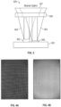
- FIG. 2 shows an example of a flood beam generated using a known optic assembly, such as depicted in FIG. 1 .
- a dot projector is also sometimes used in combination with a flood illuminator.
- the dot projector uses a second VCSEL 103 for producing a dot beam 105 to optics 107 which, in turn, produces a multitude of dots of IR light from output 108 to create a three-dimensional map of the illuminated object of interest for area and depth determinations.
- An infrared camera (not shown) captures images of the depth signature from the modulated IR flood light, and if employed, also from the dot pattern reflected back from the illuminated object of interest. Processing of the captured data can then be used for desired purposes such as, for example, facial recognition.
- One drawback associated with conventional flood illuminators is their range is limited to about 1.5m. This relatively short range greatly limits the types of applications in which this technology may be used.
- the subject matter of the present disclosure is directed to overcoming, or at least reducing the effects of, one or more of the problems set forth above.
- a shared optic assembly for combined flood and dot illumination modules includes a first high-powered VCSEL element for providing a flood beam and a second high-powered VCSEL element for providing a dot beam, where both the first and second VCSEL elements share the same optics.
- the dot beam is generated using the same level of optical power as the flood beam, but the dot beam is condensed into dots. As a result, the return signal is high enough to detect at longer range than achieved with the flood beam alone.
- a tradeoff is the received information is lower resolution since only the information where the dots are located is reflected back to the infrared camera.
- the overall system uses the same infrared camera for both dot and flood functions, but yields a short range detection with high resolution using the flood beam and longer range detection with lower resolution using the dot beam.
- the effective range increases from about 1.5m to about 6m. Further, because the flood and dot modules share the same optics, significant cost and space savings are realized.
- the present invention is directed to a VCSEL illuminator assembly, comprising:
- said first VCSEL array is located a first distance from said shared diffuser optics and said second VCSEL array is located a second distance from said shared diffuser optics that is different than said first distance.
- said first distance is approximately 2.3mm and said second distance is approximately 2mm.
- the substrate beneath the second VCSEL array is 300 ⁇ m thicker than the substrate beneath the first VCSEL array.
- the second VCSEL array is mounted on a 300 ⁇ m thick CuW spacer.
- a pitch of said first VCSEL array is an integer multiple of a pitch of the shared diffuser optics.
- the pitch of the first VCSEL array is 1x the pitch of the shared diffuser optics; wherein the pitch of the first VCSEL array is 2x the pitch of the shared diffuser optics; or wherein the pitch of the first VCSEL array is 3x the pitch of the shared diffuser optics.
- the pitch of the first VCSEL array is 1/2x the pitch of the shared diffuser optics; or wherein the pitch of the first VCSEL array is 1/3x the pitch of the shared diffuser optics.
- an X and Y delta exists between each emitter of the second VCSEL array and a closest lenslet center of the shared diffuser optics.
- both the X and Y delta is up to +/-16.5 microns.
- the emissions from the first and second VCSEL arrays have the same wavelength; wherein the emissions from the first and second VCSEL arrays have a wavelength of 940nm; or wherein the emissions from the first and second VCSEL arrays have a wavelength of 850nm.
- the wavelength of emissions from the first VCSEL array is different than the wavelength of emissions from the second VCSEL array.
- the present invention is directed to a VCSEL illuminator assembly, comprising:
- the wavelength of the first and second emissions is the same; wherein the wavelength of the first and second emissions is 940nm; or wherein the wavelength of the first and second emissions is 850nm.
- said first VCSEL array is located a first distance from said shared diffuser optics and said second VCSEL array is located a second distance from said shared diffuser optics that is different than said first distance.
- said first distance is approximately 2.3mm and said second distance is approximately 2mm.
- a pitch of said first VCSEL array is an integer multiple of a pitch of the shared diffuser optics.
- the pitch of the first VCSEL array is 1x the pitch of the shared diffuser optics.
- a high-powered VCSEL illuminator assembly 300 includes combined dot and flood illumination modules.
- the combined modules include a first VCSEL element 303 configured to provide a flood beam 305 and a second VCSEL element 302 configured to provide a dot beam 304.
- the two VCSEL elements 302, 303 are mounted on a substrate 301, and the assembly 300 includes a shared optic 306 disposed adjacent to the substrate 301.
- the assembly 300 is intended to be used as a component of an overall system, such as, for example, a facial recognition unit of a mobile device.
- the dot beam VCSEL element 302 is mounted on the substrate 301 in a defined configuration and at a defined distance (referred to as the working distance ("WD")) relative to the shared optics 306.
- the flood beam VCSEL element 303 is also mounted on the substrate 301 in a defined configuration and at a defined distance relative to the shared optic 306, where the defined distance is offset from the working distance.
- the dot beam and the flood beam are imaged by the shared optic 306 to generate output 307.
- the shared optics 306 includes a periodic diffuser optical element to generate both a dot field and a flood illumination field by using the emissions of two separate VCSELs 303, 302 in relatively close proximity to each other.
- the combined beams result in short range detection with high resolution using the flood beam and longer range detection, with lower resolution, using the dot beam.
- the dot beams concentrate the VCSEL emissions into small spots with increased intensity, the overall range of the system is increased. There is some loss in resolution for higher ranges because only the dot beams are reflected back from the object to the detector.
- the effective range of the overall system is increased from about 1.5m, using only the flood beam, to about 6m, using the dot beams.
- the IR sensor could extract depth information from the flood beam, then switch and extract depth information from the dot beam, and combine the depth information of the two modes.
- the dot mode could be used, for example, when scanning a room for dimension for furniture visualization.
- the flood could be used, for example, for facial mapping or when mapping objects close up.
- the dot and flood VCSELs share common optics, both are incorporated onto the same module, resulting in appreciable size savings over modules where optics are not shared.
- the dot field VCSEL 302 is configured to work at a pre-determined working distance from the shared optics 306 and has a pitch defined between emitters such that diffraction effects at the shared optics 306 create a dot field.
- the distance between the flood field VCSEL 303 and the shared optics 306 is offset from this working distance to avoid such diffraction effects.
- a thicker VCSEL substrate 303 or added height from the mounting substrate 301, as compared with the dot field VCSEL 302 can be used to produce the required offset distance.
- the offset distance avoids having a high contrast diffraction effect, which while desirable for the dot imager, is undesirable for the flood imager.
- diffraction effects from self-imaging the periodic diffuser array from a small source causes each individual emitter to be reimaged within an envelope of the diffuser's output profile. Emitters are appropriately pitched so that all of the single emitter array images are aligned over one another.
- the phenomenon is theoretically similar to the Lau effect, with an array of lasers being substituted in place of an illuminated first grating. See e.g., Sudol, R. (1981), Lau Effect: An Interference Phenomenon in Partially Coherent Light [Thesis], The University of Rochester, Rochester, New York .
- the second VCSEL emitter i.e., the flood VCSEL 303 layout is designed such that the differences in X and Y between the lasers and the closest diffuser freeform lenslet optical center are distributed somewhat evenly across the extent of the area of a single diffuser freeform lenslet surface, the diffraction effects can be mostly washed out.
- a VCSEL working at 2400 ⁇ m with a 20x20 emitter layout with a square pitch of 35 ⁇ (1+1/20) can provide a highly uniform X and Y difference distribution. Uniform X and Y difference distributions can be achieved in a variety of ways including rectangular, square, or hexagonal arrays of VCSELs of various pitches with specific rotation angles or specifically designed pseudo-random VCSEL arrays.
- a wavelength of 940nm is used in this example for both the dot and flood VCSEL emitters since it is a commonly used wavelength for 3-D sensing applications, the invention is not limited to any particular emitter wavelength or any particular application.
- VCSEL emitters having wavelengths of 850nm another commonly used VCSEL wavelength, may be employed. Longer or shorter wavelengths may also be used.
- the wavelength of the dot and flood VCSEL emitters need not be the same.
- the wavelength for the dot emitter may be 940nm while the wavelength of the flood emitter may be 850nm, or vice versa. Having two different wavelengths for the emitter requires a wider filter on the receiver side than if the same wavelength is emitted from both arrays.
- a filter with multiple passbands may also be used on the receiver side if the emitters have different wavelengths.
- FIG. 4A depicts an image of a projected pattern of a dot VCSEL 302 properly matched with, and at an appropriate working distance from, shared optics 306.
- FIG. 4B depicts an image of a projected pattern of a flood VCSEL 303 mismatched with, and at a 150 ⁇ m offset, or defocus, from shared optics 306.
- FIG. 5 several examples VCSEL illuminator assembly size reductions achievable with the invention are depicted.
- VCSEL illuminator assembly 100 On the left side of FIG. 5 is a prior art VCSEL illuminator assembly 100 and on the right is VCSEL illuminator assembly 300 (as described in FIG. 3 ), in accordance with an exemplary embodiment of the invention.
- the beam width for shared optics in assembly 300 is 2.7mm
- the beam width for assembly 100 with separate optics is 3.9mm.
- the beam width for shared optics in assembly 300 is 2.4mm, whereas the beam width for assembly 100 with separate optics is 3.2mm. In this example, there is a size reduction of approximately 19% achieved as a result of the invention.
- the beam width for shared optics in assembly 300 is 3mm, whereas the beam width for assembly 100 with separate optics is 4.6mm. In this example, there is a size reduction of approximately 28% achieved as a result of the invention. Thus, the percentage of the size reductions increases as the working distance increases.
- the diffuser of shared optic 306 includes a periodic array of identical, free-form surfaces that shape incident light into a desired illumination or diffused profile.
- the periodic diffuser has a square layout 601 with an X and Y pitch of 33 microns.
- Each lenslet 602 is the same and is designed to spread the incoming light over a specified field of illumination.
- a dot VCSEL 302 (in FIG. 3 ) array is depicted, in accordance with an exemplary embodiment of the invention.
- the dot VCSEL 302 array is a square layout periodic array with an X and Y pitch of 33 microns (532 emitters/8 ⁇ m oxide aperture).
- the dot VCSEL 302 array must be matched in some way to the diffuser optic.
- the dot VCSEL 302 array pitch must be some integer multiple or integer fraction of the optic pitch (i.e. 3, 2, 1, 1/2, 1/3). It has been found that 1x works well. Alternatively, much larger optics pitches and integer fraction VCSEL pitches may be used, but this results in a larger number of dots in the dot field and reduced peak intensity for each dot. Larger optics pitches and integer fractions can also result in too long of a working distance. It should also be noted that smaller optics pitches may be used along with 2x VCSEL pitches, but this arrangement can result in fabrication issues on the optics.
- FIG. 8 a flood VCSEL 303 (in FIG. 3 ) array is depicted, in accordance with an exemplary embodiment of the invention.
- the flood VCSEL 303 array is a hexagonal layout periodic array with a pitch of 40 microns rotated at 24.5 degrees (327 emitters/10 ⁇ m oxide aperture).
- any layout that results in a relatively well spreadout distribution in the difference VCSEL emitter versus the center of the closest lenslet 602 (in FIG. 6 ) will result in adequate performance.
- the flood VCSEL 303 was mounted on a 300 ⁇ m thick CuW spacer to provide the needed defocus.
- a working distance of 1.738mm i.e., 3 ⁇ 33 2 /(2 ⁇ 0.94)
- FIGS. 10 and 11 a dot field and flood field are respectively shown, as generated with the configuration described in connection with FIGS. 6-9 .
- a range of approximately 1.5m was achieved with the flood field in FIG. 11 and a range of approximately 6m was achieved with the dot field of FIG. 10 .
Landscapes
- Physics & Mathematics (AREA)
- Optics & Photonics (AREA)
- General Physics & Mathematics (AREA)
- Condensed Matter Physics & Semiconductors (AREA)
- Electromagnetism (AREA)
- Engineering & Computer Science (AREA)
- Microelectronics & Electronic Packaging (AREA)
- General Engineering & Computer Science (AREA)
- Non-Portable Lighting Devices Or Systems Thereof (AREA)
- Diffracting Gratings Or Hologram Optical Elements (AREA)
- Semiconductor Lasers (AREA)
- Optical Radar Systems And Details Thereof (AREA)
Abstract
Description
- Flood illuminators are incorporated into various products such as, for example, mobile devices and other applications, to provide 3D sensing capabilities, 3D mapping in robotics, face detection, etc. For example, with reference to
FIG. 1 , anoptic assembly 100 incorporated within, e.g., a mobile device, including a flood illuminator uses a vertical-cavity surface-emitting laser (VCSEL) 102 for providing aflood beam 104 tooptics 106 which, in turn, produces a uniform field of illumination of infrared (IR) light fromoutput 108 onto an object or person of interest (not shown).FIG. 2 shows an example of a flood beam generated using a known optic assembly, such as depicted inFIG. 1 . - A dot projector is also sometimes used in combination with a flood illuminator. The dot projector uses a second VCSEL 103 for producing a
dot beam 105 tooptics 107 which, in turn, produces a multitude of dots of IR light fromoutput 108 to create a three-dimensional map of the illuminated object of interest for area and depth determinations. An infrared camera (not shown) captures images of the depth signature from the modulated IR flood light, and if employed, also from the dot pattern reflected back from the illuminated object of interest. Processing of the captured data can then be used for desired purposes such as, for example, facial recognition. One drawback associated with conventional flood illuminators is their range is limited to about 1.5m. This relatively short range greatly limits the types of applications in which this technology may be used. - The subject matter of the present disclosure is directed to overcoming, or at least reducing the effects of, one or more of the problems set forth above.
- A shared optic assembly for combined flood and dot illumination modules is disclosed. The shared optic assembly includes a first high-powered VCSEL element for providing a flood beam and a second high-powered VCSEL element for providing a dot beam, where both the first and second VCSEL elements share the same optics. The dot beam is generated using the same level of optical power as the flood beam, but the dot beam is condensed into dots. As a result, the return signal is high enough to detect at longer range than achieved with the flood beam alone. A tradeoff is the received information is lower resolution since only the information where the dots are located is reflected back to the infrared camera. The overall system uses the same infrared camera for both dot and flood functions, but yields a short range detection with high resolution using the flood beam and longer range detection with lower resolution using the dot beam. Through the use of the invention, the effective range increases from about 1.5m to about 6m. Further, because the flood and dot modules share the same optics, significant cost and space savings are realized.
- The foregoing summary is not intended to summarize each potential embodiment or every aspect of the present disclosure.
- According to a first aspect, the present invention is directed to a VCSEL illuminator assembly, comprising:
- a first VCSEL array for generating a dot beam;
- a second VCSEL array, and adjacent to said first VCSEL array, for generating a flood beam; and
- diffuser optics shared by said first and second VCSEL arrays for receiving emissions from said first and second VCSEL arrays.
- According to a first embodiment of the first aspect, said first VCSEL array is located a first distance from said shared diffuser optics and said second VCSEL array is located a second distance from said shared diffuser optics that is different than said first distance.
- According to a second embodiment of the first aspect with the first embodiment of the first aspect, said first distance is approximately 2.3mm and said second distance is approximately 2mm.
- According to a third embodiment of the first aspect with the second embodiment of the first aspect, the substrate beneath the second VCSEL array is 300µm thicker than the substrate beneath the first VCSEL array.
- According to a fourth embodiment of the first aspect with the third embodiment of the first aspect, the second VCSEL array is mounted on a 300µm thick CuW spacer.
- According to a fifth embodiment of the first aspect, a pitch of said first VCSEL array is an integer multiple of a pitch of the shared diffuser optics.
- According to a sixth embodiment of the first aspect with the fifth embodiment of the first aspect, the pitch of the first VCSEL array is 1x the pitch of the shared diffuser optics; wherein the pitch of the first VCSEL array is 2x the pitch of the shared diffuser optics; or wherein the pitch of the first VCSEL array is 3x the pitch of the shared diffuser optics.
- According to a seventh embodiment of the first aspect, a pitch of said first VCSEL array is an integer fraction of a pitch of the shared diffuser optics.
- According to a eighth embodiment of the first aspect with the sixth embodiment of the first aspect, the pitch of the first VCSEL array is 1/2x the pitch of the shared diffuser optics; or wherein the pitch of the first VCSEL array is 1/3x the pitch of the shared diffuser optics.
- According to a ninth embodiment of the first aspect with the seventh embodiment of the first aspect, an X and Y delta exists between each emitter of the second VCSEL array and a closest lenslet center of the shared diffuser optics.
- According to a tenth embodiment of the first aspect with the ninth embodiment of the first aspect, both the X and Y delta is up to +/-16.5 microns.
- According to a eleventh embodiment of the first aspect, the emissions from the first and second VCSEL arrays have the same wavelength; wherein the emissions from the first and second VCSEL arrays have a wavelength of 940nm; or wherein the emissions from the first and second VCSEL arrays have a wavelength of 850nm.
- According to a twelfth embodiment of the first aspect, the wavelength of emissions from the first VCSEL array is different than the wavelength of emissions from the second VCSEL array.
- According to a second aspect, the present invention is directed to a VCSEL illuminator assembly, comprising:
- a first VCSEL array for generating a first emission;
- a second VCSEL array, adjacent to the first VCSEL array, for generating a second emission; and
- diffuser optics shared by the first and second VCSEL arrays for receiving the first and second emissions,
- wherein the first VCSEL array is configured such that a diffraction effect is created at the shared diffuser optics and the second VCSEL array is configured such that no diffraction effect is created at the shared diffuser optics.
- According to a first embodiment of the second aspect, the wavelength of the first and second emissions is the same; wherein the wavelength of the first and second emissions is 940nm; or wherein the wavelength of the first and second emissions is 850nm.
- According to a second embodiment of the second aspect, the wavelength of the first emissions is different than the wavelength of the second emissions.
- According to a third embodiment of the second aspect, said first VCSEL array is located a first distance from said shared diffuser optics and said second VCSEL array is located a second distance from said shared diffuser optics that is different than said first distance.
- According to a fourth embodiment of the second aspect with the third embodiment of the second aspect, said first distance is approximately 2.3mm and said second distance is approximately 2mm.
- According to a fifth embodiment of the second aspect, a pitch of said first VCSEL array is an integer multiple of a pitch of the shared diffuser optics.
- According to a sixth embodiment of the second aspect, the pitch of the first VCSEL array is 1x the pitch of the shared diffuser optics.
-
-
FIG. 1 illustrates an optic assembly with separate dot and flood illumination modules, as known in the art; -
FIG. 2 illustrates a flood beam generated using a standard randomized diffuser, as known in the art; -
FIG. 3 illustrates a shared optic assembly with combined dot and flood illumination modules and shared optics, in accordance with an exemplary embodiment of the invention; -
FIG. 4A illustrates a dot projector pattern generated in accordance with an exemplary embodiment of the invention; -
FIG. 4B illustrates a flood beam generated in accordance with an exemplary embodiment of the invention; -
FIG. 5 shows expected space savings based on working distance, in accordance with exemplary embodiments of the invention; -
FIG. 6 illustrates a configuration of shared optics, in accordance with an exemplary embodiment of the invention; -
FIG. 7 illustrates a dot VCSEL layout, in accordance with an exemplary embodiment of the invention; -
FIG 8 illustrates a flood VCSEL layout, in accordance with an exemplary embodiment of the invention; -
FIG. 9 illustrates a distribution of the X-axis and Y-axis difference between individual flood VCSEL emitters (ofFIG. 8 ), and the closest diffuser lenslet center (ofFIG. 6 ), in accordance with an exemplary embodiment of the invention; -
FIG. 10 illustrates a dot field generated using an exemplary embodiment of the invention; and -
FIG. 11 illustrates a flood field generated using an exemplary embodiment of the invention. - Referring to
FIG. 3 , a high-poweredVCSEL illuminator assembly 300 includes combined dot and flood illumination modules. The combined modules include afirst VCSEL element 303 configured to provide aflood beam 305 and asecond VCSEL element 302 configured to provide adot beam 304. The twoVCSEL elements substrate 301, and theassembly 300 includes a sharedoptic 306 disposed adjacent to thesubstrate 301. Theassembly 300 is intended to be used as a component of an overall system, such as, for example, a facial recognition unit of a mobile device. - The dot
beam VCSEL element 302 is mounted on thesubstrate 301 in a defined configuration and at a defined distance (referred to as the working distance ("WD")) relative to the sharedoptics 306. The floodbeam VCSEL element 303 is also mounted on thesubstrate 301 in a defined configuration and at a defined distance relative to the sharedoptic 306, where the defined distance is offset from the working distance. The dot beam and the flood beam are imaged by the sharedoptic 306 to generateoutput 307. - As explained in greater detail below in connection with an exemplary embodiment, the shared
optics 306 includes a periodic diffuser optical element to generate both a dot field and a flood illumination field by using the emissions of twoseparate VCSELs - In one example of an application of the invention, the IR sensor could extract depth information from the flood beam, then switch and extract depth information from the dot beam, and combine the depth information of the two modes. The dot mode could be used, for example, when scanning a room for dimension for furniture visualization. The flood could be used, for example, for facial mapping or when mapping objects close up. Moreover, because the dot and flood VCSELs share common optics, both are incorporated onto the same module, resulting in appreciable size savings over modules where optics are not shared.
- Still referring generally to
FIG. 3 , thedot field VCSEL 302 is configured to work at a pre-determined working distance from the sharedoptics 306 and has a pitch defined between emitters such that diffraction effects at the sharedoptics 306 create a dot field. The distance between theflood field VCSEL 303 and the sharedoptics 306 is offset from this working distance to avoid such diffraction effects. For example, athicker VCSEL substrate 303 or added height from the mountingsubstrate 301, as compared with thedot field VCSEL 302 can be used to produce the required offset distance. The offset distance avoids having a high contrast diffraction effect, which while desirable for the dot imager, is undesirable for the flood imager. - Still referring generally to
FIG. 3 , diffraction effects from self-imaging the periodic diffuser array from a small source causes each individual emitter to be reimaged within an envelope of the diffuser's output profile. Emitters are appropriately pitched so that all of the single emitter array images are aligned over one another. The phenomenon is theoretically similar to the Lau effect, with an array of lasers being substituted in place of an illuminated first grating. See e.g., Sudol, R. (1981), Lau Effect: An Interference Phenomenon in Partially Coherent Light [Thesis], The University of Rochester, Rochester, New York. The theory provides that high contrast images can be achieved at a distance Z = np2/2λ, where n is a positive integer, p is the diffuser array pitch, and λ is the wavelength of light. - As this high contrast phenomenon occurs only at specific distances, an offset or defocus between the VCSEL laser array and the periodic diffuser array can diminish the contrast. If the second VCSEL emitter (i.e., the flood VCSEL 303) layout is designed such that the differences in X and Y between the lasers and the closest diffuser freeform lenslet optical center are distributed somewhat evenly across the extent of the area of a single diffuser freeform lenslet surface, the diffraction effects can be mostly washed out.
- This can be done through a straightforward configuration. For example, a square diffuser array with a 35µm pitch can have high contrast at a distance of 2606µm for n = 4 and λ = 940nm. A VCSEL working at 2400µm with a 20x20 emitter layout with a square pitch of 35∗(1+1/20) can provide a highly uniform X and Y difference distribution. Uniform X and Y difference distributions can be achieved in a variety of ways including rectangular, square, or hexagonal arrays of VCSELs of various pitches with specific rotation angles or specifically designed pseudo-random VCSEL arrays. It should be noted that although a wavelength of 940nm is used in this example for both the dot and flood VCSEL emitters since it is a commonly used wavelength for 3-D sensing applications, the invention is not limited to any particular emitter wavelength or any particular application. For example, VCSEL emitters having wavelengths of 850nm, another commonly used VCSEL wavelength, may be employed. Longer or shorter wavelengths may also be used. Further, the wavelength of the dot and flood VCSEL emitters need not be the same. For example, the wavelength for the dot emitter may be 940nm while the wavelength of the flood emitter may be 850nm, or vice versa. Having two different wavelengths for the emitter requires a wider filter on the receiver side than if the same wavelength is emitted from both arrays. Alternatively, a filter with multiple passbands may also be used on the receiver side if the emitters have different wavelengths.
-
FIG. 4A depicts an image of a projected pattern of adot VCSEL 302 properly matched with, and at an appropriate working distance from, sharedoptics 306. -
FIG. 4B depicts an image of a projected pattern of aflood VCSEL 303 mismatched with, and at a 150µm offset, or defocus, from sharedoptics 306. - Referring now to
FIG. 5 , several examples VCSEL illuminator assembly size reductions achievable with the invention are depicted. On the left side ofFIG. 5 is a prior artVCSEL illuminator assembly 100 and on the right is VCSEL illuminator assembly 300 (as described inFIG. 3 ), in accordance with an exemplary embodiment of the invention. In the illustrated example, and with references to the table (middle row), for a working distance of 2.3mm, the beam width for shared optics inassembly 300 is 2.7mm, whereas the beam width forassembly 100 with separate optics is 3.9mm. Thus, in this example, there is a size reduction of approximately 24% achieved as a result of the invention. - For a smaller working distance of 1.7mm, the beam width for shared optics in
assembly 300 is 2.4mm, whereas the beam width forassembly 100 with separate optics is 3.2mm. In this example, there is a size reduction of approximately 19% achieved as a result of the invention. Lastly, for a larger working distance of 2.8mm, the beam width for shared optics inassembly 300 is 3mm, whereas the beam width forassembly 100 with separate optics is 4.6mm. In this example, there is a size reduction of approximately 28% achieved as a result of the invention. Thus, the percentage of the size reductions increases as the working distance increases. - Referring now to
FIG. 6 , the diffuser of shared optic 306 (inFIG. 3 ), includes a periodic array of identical, free-form surfaces that shape incident light into a desired illumination or diffused profile. In this exemplary embodiment, the periodic diffuser has asquare layout 601 with an X and Y pitch of 33 microns. Eachlenslet 602 is the same and is designed to spread the incoming light over a specified field of illumination. In this example, the working distance ("WD"), i.e., the distance between thedot field VCSEL 302 and sharedoptics 306, is 2.32mm (i.e., np2/2λ = (4∗332/(2∗0.94) = 2.32mm). - Referring now to
FIG. 7 , a dot VCSEL 302 (inFIG. 3 ) array is depicted, in accordance with an exemplary embodiment of the invention. Thedot VCSEL 302 array is a square layout periodic array with an X and Y pitch of 33 microns (532 emitters/8µm oxide aperture). Notably, thedot VCSEL 302 array must be matched in some way to the diffuser optic. - The
dot VCSEL 302 array pitch must be some integer multiple or integer fraction of the optic pitch (i.e. 3, 2, 1, 1/2, 1/3). It has been found that 1x works well. Alternatively, much larger optics pitches and integer fraction VCSEL pitches may be used, but this results in a larger number of dots in the dot field and reduced peak intensity for each dot. Larger optics pitches and integer fractions can also result in too long of a working distance. It should also be noted that smaller optics pitches may be used along with 2x VCSEL pitches, but this arrangement can result in fabrication issues on the optics. - Turning to
FIG. 8 , a flood VCSEL 303 (inFIG. 3 ) array is depicted, in accordance with an exemplary embodiment of the invention. Theflood VCSEL 303 array is a hexagonal layout periodic array with a pitch of 40 microns rotated at 24.5 degrees (327 emitters/10µm oxide aperture). Notably, for theflood VCSEL 303, any layout that results in a relatively well spreadout distribution in the difference VCSEL emitter versus the center of the closest lenslet 602 (inFIG. 6 ) will result in adequate performance. In this exemplary embodiment, theflood VCSEL 303 was mounted on a 300µm thick CuW spacer to provide the needed defocus. In this instance, a working distance of 1.738mm (i.e., 3∗332/(2∗0.94)) would be at another high contrast distance, so approximately half way between distances corresponding to n = 3 and n = 4, resulting in a distance of approximately 2mm, was found to work well. - Referring now to
FIG. 9 , a distribution of the X and Y difference betweenindividual flood VCSEL 303 emitters and theclosest diffuser lenslet 602 center is depicted, as explained in connection withFIG. 8 . Each point in the scatter plot represents the X and Y delta between a single VCSEL emitter and the closest diffuser lenslet center. In the examples depicted inFIGS. 6 and8 , the range of the delta is +/-16.5µm in both dimensions, since the size of thelenslet 602 is 33um. Essentially, the VCSEL emitters are scattered around so that they are as far from matching the periodicity of the diffuser lenslets. This arrangement helps wash out any remaining diffraction effects. - Referring now to
FIGS. 10 and 11 , a dot field and flood field are respectively shown, as generated with the configuration described in connection withFIGS. 6-9 . Using the principles and specific arrangements described herein, a range of approximately 1.5m was achieved with the flood field inFIG. 11 and a range of approximately 6m was achieved with the dot field ofFIG. 10 . - The foregoing description of preferred and other embodiments is not intended to limit or restrict the scope or applicability of the inventive concepts conceived of by the Applicants. It will be appreciated with the benefit of the present disclosure that features described above in accordance with any embodiment or aspect of the disclosed subject matter can be utilized, either alone or in combination, with any other described feature, in any other embodiment or aspect of the disclosed subject matter.
- In exchange for disclosing the inventive concepts contained herein, the Applicants desire all patent rights afforded by the appended claims. Therefore, it is intended that the appended claims include all modifications and alterations to the full extent that they come within the scope of the following claims or the equivalents thereof.
Claims (15)
- A VCSEL illuminator assembly (300), comprising:a first VCSEL array for generating a dot beam;a second VCSEL array, and adjacent to said first VCSEL array, for generating a flood beam; anddiffuser optics (306) shared by said first and second VCSEL arrays for receiving emissions from said first and second VCSEL arrays.
- The VCSEL illuminator assembly (300) of claim 1, wherein said first VCSEL array is located a first distance from said shared diffuser optics (306) and said second VCSEL array is located a second distance from said shared diffuser optics (306) that is different than said first distance, wherein preferably said first distance is approximately 2.3mm and said second distance is approximately 2mm, wherein more preferably the substrate beneath the second VCSEL array is 300µm thicker than the substrate beneath the first VCSEL array, and wherein even more preferably the second VCSEL array is mounted on a 300µm thick CuW spacer.
- The VCSEL illuminator assembly (300) of claim 1, wherein a pitch of said first VCSEL array is an integer multiple of a pitch of the shared diffuser optics (306).
- The VCSEL illuminator assembly (300) of claim 3, wherein the pitch of the first VCSEL array is 1x the pitch of the shared diffuser optics (306); wherein the pitch of the first VCSEL array is 2x the pitch of the shared diffuser optics (306); or wherein the pitch of the first VCSEL array is 3x the pitch of the shared diffuser optics (306).
- The VCSEL illuminator assembly (300) of claim 1, wherein a pitch of said first VCSEL array is an integer fraction of a pitch of the shared diffuser optics (306).
- The VCSEL illuminator assembly (300) of claim 5, wherein the pitch of the first VCSEL array is 1/2x the pitch of the shared diffuser optics (306); or wherein the pitch of the first VCSEL array is 1/3x the pitch of the shared diffuser optics (306).
- The VCSEL illuminator assembly (300) of claim 5, wherein an X and Y delta exists between each emitter of the second VCSEL array and a closest lenslet center of the shared diffuser optics (306), wherein preferably both the X and Y delta is up to +/-16.5 microns.
- The VCSEL illuminator assembly (300) of claim 1, wherein the emissions from the first and second VCSEL arrays have the same wavelength; wherein the emissions from the first and second VCSEL arrays have a wavelength of 940nm; or wherein the emissions from the first and second VCSEL arrays have a wavelength of 850nm.
- The VCSEL illuminator assembly (300) of claim 1, wherein the wavelength of emissions from the first VCSEL array is different than the wavelength of emissions from the second VCSEL array.
- A VCSEL illuminator assembly (300), comprising:a first VCSEL array for generating a first emission;a second VCSEL array, adjacent to the first VCSEL array, for generating a second emission; anddiffuser optics (306) shared by the first and second VCSEL arrays for receiving the first and second emissions,wherein the first VCSEL array is configured such that a diffraction effect is created at the shared diffuser optics (306) and the second VCSEL array is configured such that no diffraction effect is created at the shared diffuser optics (306).
- The VCSEL illuminator assembly (300) of claim 10, wherein the wavelength of the first and second emissions is the same; wherein the wavelength of the first and second emissions is 940nm; or wherein the wavelength of the first and second emissions is 850nm.
- The VCSEL illuminator assembly (300) of claim 10, wherein the wavelength of the first emissions is different than the wavelength of the second emissions.
- The VCSEL illuminator assembly (300) of claim 10, wherein said first VCSEL array is located a first distance from said shared diffuser optics (306) and said second VCSEL array is located a second distance from said shared diffuser optics (306) that is different than said first distance, wherein preferably said first distance is approximately 2.3mm and said second distance is approximately 2mm.
- The VCSEL illuminator assembly (300) of claim 10, wherein a pitch of said first VCSEL array is an integer multiple of a pitch of the shared diffuser optics (306).
- The VCSEL illuminator assembly (300) of claim 14, wherein the pitch of the first VCSEL array is 1x the pitch of the shared diffuser optics (306).
Applications Claiming Priority (1)
| Application Number | Priority Date | Filing Date | Title |
|---|---|---|---|
| US17/450,368 US12163634B2 (en) | 2021-10-08 | 2021-10-08 | Shared optic assembly for combined dot and flood illumination modules |
Publications (1)
| Publication Number | Publication Date |
|---|---|
| EP4163668A1 true EP4163668A1 (en) | 2023-04-12 |
Family
ID=83900071
Family Applications (1)
| Application Number | Title | Priority Date | Filing Date |
|---|---|---|---|
| EP22198788.6A Pending EP4163668A1 (en) | 2021-10-08 | 2022-09-29 | Shared optic assembly for combined dot and flood illumination modules |
Country Status (4)
| Country | Link |
|---|---|
| US (1) | US12163634B2 (en) |
| EP (1) | EP4163668A1 (en) |
| JP (1) | JP2023057023A (en) |
| CN (1) | CN115963685A (en) |
Citations (3)
| Publication number | Priority date | Publication date | Assignee | Title |
|---|---|---|---|---|
| CN108169981A (en) * | 2018-01-15 | 2018-06-15 | 深圳奥比中光科技有限公司 | Multifunctional Lighting Module |
| WO2021075340A1 (en) * | 2019-10-15 | 2021-04-22 | ソニーセミコンダクタソリューションズ株式会社 | Illumination device and ranging device |
| WO2021198269A1 (en) * | 2020-03-31 | 2021-10-07 | Trumpf Photonic Components Gmbh | Illumination device for a distance measurement camera system, a corresponding illumination method and a tof camera system |
Family Cites Families (8)
| Publication number | Priority date | Publication date | Assignee | Title |
|---|---|---|---|---|
| KR20050008767A (en) * | 2002-06-03 | 2005-01-21 | 소니 가부시끼 가이샤 | Two-wavelength optical element |
| US8644357B2 (en) * | 2011-01-11 | 2014-02-04 | Ii-Vi Incorporated | High reliability laser emitter modules |
| JP6245629B2 (en) * | 2013-03-26 | 2017-12-13 | 大学共同利用機関法人自然科学研究機構 | In-vehicle ignition system using semiconductor laser pumped solid-state laser device |
| US10827163B2 (en) * | 2016-08-09 | 2020-11-03 | Facebook Technologies, Llc | Multiple emitter illumination source for depth information determination |
| KR102536534B1 (en) * | 2018-06-22 | 2023-05-25 | 엘지이노텍 주식회사 | Camera module |
| JP7321834B2 (en) * | 2019-08-26 | 2023-08-07 | ソニーセミコンダクタソリューションズ株式会社 | Lighting device and ranging module |
| US11762212B2 (en) * | 2020-03-12 | 2023-09-19 | Stmicroelectronics (Research & Development) Limited | Diffuse illumination system having VCSEL emitters and array of nanostructures |
| KR102740171B1 (en) * | 2020-03-16 | 2024-12-09 | 엘지이노텍 주식회사 | Camera module |
-
2021
- 2021-10-08 US US17/450,368 patent/US12163634B2/en active Active
-
2022
- 2022-07-28 CN CN202210903745.3A patent/CN115963685A/en active Pending
- 2022-08-17 JP JP2022129880A patent/JP2023057023A/en active Pending
- 2022-09-29 EP EP22198788.6A patent/EP4163668A1/en active Pending
Patent Citations (3)
| Publication number | Priority date | Publication date | Assignee | Title |
|---|---|---|---|---|
| CN108169981A (en) * | 2018-01-15 | 2018-06-15 | 深圳奥比中光科技有限公司 | Multifunctional Lighting Module |
| WO2021075340A1 (en) * | 2019-10-15 | 2021-04-22 | ソニーセミコンダクタソリューションズ株式会社 | Illumination device and ranging device |
| WO2021198269A1 (en) * | 2020-03-31 | 2021-10-07 | Trumpf Photonic Components Gmbh | Illumination device for a distance measurement camera system, a corresponding illumination method and a tof camera system |
Non-Patent Citations (1)
| Title |
|---|
| SUDOL, R.: "Lau Effect: An Interference Phenomenon in Partially Coherent Light [Thesis", 1981, THE UNIVERSITY OF ROCHESTER |
Also Published As
| Publication number | Publication date |
|---|---|
| JP2023057023A (en) | 2023-04-20 |
| CN115963685A (en) | 2023-04-14 |
| US12163634B2 (en) | 2024-12-10 |
| US20230116691A1 (en) | 2023-04-13 |
Similar Documents
| Publication | Publication Date | Title |
|---|---|---|
| US11852463B2 (en) | Projectors of structured light | |
| KR102626258B1 (en) | Optical designs and detector designs for improved resolution in LiDAR systems | |
| TWI838490B (en) | Time of flight-based three-dimensional sensing system | |
| KR102762083B1 (en) | Light source device, detection device, and electronic device | |
| US10408922B2 (en) | Optoelectronic module with low- and high-power illumination modes | |
| EP1561084B1 (en) | Structured light projector | |
| KR20230000988A (en) | Line pattern projector for use in three-dimensional distance measurement system | |
| CN115427830A (en) | Illumination device for a distance measuring camera system, corresponding illumination method and TOF camera system | |
| KR20210020758A (en) | Micro-optics and optoelectronics module including the same | |
| US20230003843A1 (en) | Transmission unit and lidar device with optical homogenizer | |
| US12163634B2 (en) | Shared optic assembly for combined dot and flood illumination modules | |
| EP3411659B1 (en) | Illumination modules and optoelectronic systems | |
| CN1591468B (en) | Method and device for optical navigation | |
| US6845119B2 (en) | Laser illuminating apparatus for illuminating a strip-shaped or linear area | |
| US20230020619A1 (en) | Multi-beam scanning system | |
| EP4403995A1 (en) | Systems and methods for projecting illumination from a device edge | |
| US20120300489A1 (en) | Light Generator | |
| CN113391514B (en) | 3D imaging device and method | |
| CN117906588A (en) | Optical navigation device for increasing depth of field | |
| KR20230158032A (en) | Systems, methods, and devices for combining multiple optical component arrays | |
| WO2026004630A1 (en) | Light-emitting module | |
| JP2024017519A (en) | Measuring device, receiver, and emitter | |
| JP2024103433A5 (en) | ||
| HK40054239A (en) | Time of flight-based three-dimensional sensing system |
Legal Events
| Date | Code | Title | Description |
|---|---|---|---|
| PUAI | Public reference made under article 153(3) epc to a published international application that has entered the european phase |
Free format text: ORIGINAL CODE: 0009012 |
|
| STAA | Information on the status of an ep patent application or granted ep patent |
Free format text: STATUS: THE APPLICATION HAS BEEN PUBLISHED |
|
| AK | Designated contracting states |
Kind code of ref document: A1 Designated state(s): AL AT BE BG CH CY CZ DE DK EE ES FI FR GB GR HR HU IE IS IT LI LT LU LV MC MK MT NL NO PL PT RO RS SE SI SK SM TR |
|
| P01 | Opt-out of the competence of the unified patent court (upc) registered |
Effective date: 20230515 |
|
| STAA | Information on the status of an ep patent application or granted ep patent |
Free format text: STATUS: REQUEST FOR EXAMINATION WAS MADE |
|
| 17P | Request for examination filed |
Effective date: 20230926 |
|
| RBV | Designated contracting states (corrected) |
Designated state(s): AL AT BE BG CH CY CZ DE DK EE ES FI FR GB GR HR HU IE IS IT LI LT LU LV MC MK MT NL NO PL PT RO RS SE SI SK SM TR |
|
| STAA | Information on the status of an ep patent application or granted ep patent |
Free format text: STATUS: EXAMINATION IS IN PROGRESS |
|
| 17Q | First examination report despatched |
Effective date: 20251203 |