EP4162869A1 - Electronic device - Google Patents
Electronic device Download PDFInfo
- Publication number
- EP4162869A1 EP4162869A1 EP22761343.7A EP22761343A EP4162869A1 EP 4162869 A1 EP4162869 A1 EP 4162869A1 EP 22761343 A EP22761343 A EP 22761343A EP 4162869 A1 EP4162869 A1 EP 4162869A1
- Authority
- EP
- European Patent Office
- Prior art keywords
- electrode
- electronic device
- temperature sensor
- contact member
- negative
- Prior art date
- Legal status (The legal status is an assumption and is not a legal conclusion. Google has not performed a legal analysis and makes no representation as to the accuracy of the status listed.)
- Granted
Links
Images



Classifications
-
- H—ELECTRICITY
- H05—ELECTRIC TECHNIQUES NOT OTHERWISE PROVIDED FOR
- H05K—PRINTED CIRCUITS; CASINGS OR CONSTRUCTIONAL DETAILS OF ELECTRIC APPARATUS; MANUFACTURE OF ASSEMBLAGES OF ELECTRICAL COMPONENTS
- H05K7/00—Constructional details common to different types of electric apparatus
- H05K7/14—Mounting supporting structure in casing or on frame or rack
- H05K7/1422—Printed circuit boards receptacles, e.g. stacked structures, electronic circuit modules or box like frames
- H05K7/1427—Housings
-
- A—HUMAN NECESSITIES
- A61—MEDICAL OR VETERINARY SCIENCE; HYGIENE
- A61B—DIAGNOSIS; SURGERY; IDENTIFICATION
- A61B5/00—Measuring for diagnostic purposes; Identification of persons
- A61B5/68—Arrangements of detecting, measuring or recording means, e.g. sensors, in relation to patient
- A61B5/6801—Arrangements of detecting, measuring or recording means, e.g. sensors, in relation to patient specially adapted to be attached to or worn on the body surface
- A61B5/6802—Sensor mounted on worn items
- A61B5/681—Wristwatch-type devices
-
- A—HUMAN NECESSITIES
- A61—MEDICAL OR VETERINARY SCIENCE; HYGIENE
- A61B—DIAGNOSIS; SURGERY; IDENTIFICATION
- A61B5/00—Measuring for diagnostic purposes; Identification of persons
- A61B5/02—Detecting, measuring or recording for evaluating the cardiovascular system, e.g. pulse, heart rate, blood pressure or blood flow
- A61B5/0205—Simultaneously evaluating both cardiovascular conditions and different types of body conditions, e.g. heart and respiratory condition
- A61B5/02055—Simultaneously evaluating both cardiovascular condition and temperature
-
- A—HUMAN NECESSITIES
- A61—MEDICAL OR VETERINARY SCIENCE; HYGIENE
- A61B—DIAGNOSIS; SURGERY; IDENTIFICATION
- A61B5/00—Measuring for diagnostic purposes; Identification of persons
- A61B5/24—Detecting, measuring or recording bioelectric or biomagnetic signals of the body or parts thereof
- A61B5/25—Bioelectric electrodes therefor
- A61B5/251—Means for maintaining electrode contact with the body
- A61B5/256—Wearable electrodes, e.g. having straps or bands
-
- A—HUMAN NECESSITIES
- A61—MEDICAL OR VETERINARY SCIENCE; HYGIENE
- A61B—DIAGNOSIS; SURGERY; IDENTIFICATION
- A61B5/00—Measuring for diagnostic purposes; Identification of persons
- A61B5/24—Detecting, measuring or recording bioelectric or biomagnetic signals of the body or parts thereof
- A61B5/25—Bioelectric electrodes therefor
- A61B5/279—Bioelectric electrodes therefor specially adapted for particular uses
- A61B5/28—Bioelectric electrodes therefor specially adapted for particular uses for electrocardiography [ECG]
-
- A—HUMAN NECESSITIES
- A61—MEDICAL OR VETERINARY SCIENCE; HYGIENE
- A61B—DIAGNOSIS; SURGERY; IDENTIFICATION
- A61B5/00—Measuring for diagnostic purposes; Identification of persons
- A61B5/24—Detecting, measuring or recording bioelectric or biomagnetic signals of the body or parts thereof
- A61B5/25—Bioelectric electrodes therefor
- A61B5/279—Bioelectric electrodes therefor specially adapted for particular uses
- A61B5/28—Bioelectric electrodes therefor specially adapted for particular uses for electrocardiography [ECG]
- A61B5/282—Holders for multiple electrodes
-
- G—PHYSICS
- G01—MEASURING; TESTING
- G01K—MEASURING TEMPERATURE; MEASURING QUANTITY OF HEAT; THERMALLY-SENSITIVE ELEMENTS NOT OTHERWISE PROVIDED FOR
- G01K13/00—Thermometers specially adapted for specific purposes
- G01K13/20—Clinical contact thermometers for use with humans or animals
-
- H—ELECTRICITY
- H05—ELECTRIC TECHNIQUES NOT OTHERWISE PROVIDED FOR
- H05K—PRINTED CIRCUITS; CASINGS OR CONSTRUCTIONAL DETAILS OF ELECTRIC APPARATUS; MANUFACTURE OF ASSEMBLAGES OF ELECTRICAL COMPONENTS
- H05K1/00—Printed circuits
- H05K1/18—Printed circuits structurally associated with non-printed electric components
- H05K1/181—Printed circuits structurally associated with non-printed electric components associated with surface mounted components
-
- A—HUMAN NECESSITIES
- A61—MEDICAL OR VETERINARY SCIENCE; HYGIENE
- A61B—DIAGNOSIS; SURGERY; IDENTIFICATION
- A61B2562/00—Details of sensors; Constructional details of sensor housings or probes; Accessories for sensors
- A61B2562/02—Details of sensors specially adapted for in-vivo measurements
- A61B2562/0209—Special features of electrodes classified in A61B5/24, A61B5/25, A61B5/283, A61B5/291, A61B5/296, A61B5/053
-
- A—HUMAN NECESSITIES
- A61—MEDICAL OR VETERINARY SCIENCE; HYGIENE
- A61B—DIAGNOSIS; SURGERY; IDENTIFICATION
- A61B2562/00—Details of sensors; Constructional details of sensor housings or probes; Accessories for sensors
- A61B2562/14—Coupling media or elements to improve sensor contact with skin or tissue
-
- A—HUMAN NECESSITIES
- A61—MEDICAL OR VETERINARY SCIENCE; HYGIENE
- A61B—DIAGNOSIS; SURGERY; IDENTIFICATION
- A61B2562/00—Details of sensors; Constructional details of sensor housings or probes; Accessories for sensors
- A61B2562/16—Details of sensor housings or probes; Details of structural supports for sensors
- A61B2562/166—Details of sensor housings or probes; Details of structural supports for sensors the sensor is mounted on a specially adapted printed circuit board
-
- A—HUMAN NECESSITIES
- A61—MEDICAL OR VETERINARY SCIENCE; HYGIENE
- A61B—DIAGNOSIS; SURGERY; IDENTIFICATION
- A61B5/00—Measuring for diagnostic purposes; Identification of persons
- A61B5/02—Detecting, measuring or recording for evaluating the cardiovascular system, e.g. pulse, heart rate, blood pressure or blood flow
- A61B5/024—Measuring pulse rate or heart rate
- A61B5/02416—Measuring pulse rate or heart rate using photoplethysmograph signals, e.g. generated by infrared radiation
-
- A—HUMAN NECESSITIES
- A61—MEDICAL OR VETERINARY SCIENCE; HYGIENE
- A61B—DIAGNOSIS; SURGERY; IDENTIFICATION
- A61B5/00—Measuring for diagnostic purposes; Identification of persons
- A61B5/02—Detecting, measuring or recording for evaluating the cardiovascular system, e.g. pulse, heart rate, blood pressure or blood flow
- A61B5/024—Measuring pulse rate or heart rate
- A61B5/02438—Measuring pulse rate or heart rate with portable devices, e.g. worn by the patient
-
- A—HUMAN NECESSITIES
- A61—MEDICAL OR VETERINARY SCIENCE; HYGIENE
- A61B—DIAGNOSIS; SURGERY; IDENTIFICATION
- A61B5/00—Measuring for diagnostic purposes; Identification of persons
- A61B5/24—Detecting, measuring or recording bioelectric or biomagnetic signals of the body or parts thereof
- A61B5/316—Modalities, i.e. specific diagnostic methods
- A61B5/318—Heart-related electrical modalities, e.g. electrocardiography [ECG]
- A61B5/332—Portable devices specially adapted therefor
-
- G—PHYSICS
- G04—HOROLOGY
- G04G—ELECTRONIC TIME-PIECES
- G04G21/00—Input or output devices integrated in time-pieces
- G04G21/02—Detectors of external physical values, e.g. temperature
- G04G21/025—Detectors of external physical values, e.g. temperature for measuring physiological data
-
- H—ELECTRICITY
- H05—ELECTRIC TECHNIQUES NOT OTHERWISE PROVIDED FOR
- H05K—PRINTED CIRCUITS; CASINGS OR CONSTRUCTIONAL DETAILS OF ELECTRIC APPARATUS; MANUFACTURE OF ASSEMBLAGES OF ELECTRICAL COMPONENTS
- H05K2201/00—Indexing scheme relating to printed circuits covered by H05K1/00
- H05K2201/10—Details of components or other objects attached to or integrated in a printed circuit board
- H05K2201/10007—Types of components
- H05K2201/10151—Sensor
Definitions
- This application relates to the technical field of electronic devices, and in particular, to an electronic device.
- This application provides an electronic device, to improve measurement accuracy of a temperature sensor, shorten a measurement time of the temperature sensor, and improve sensitivity of the temperature sensor.
- the electronic device includes a shell, a contact member, a temperature sensor, and a circuit board.
- the shell has an accommodating space.
- the contact member is arranged on the shell, and at least part of a surface of the contact member forms an outer surface of the electronic device. That is to say, a part of the surface of the contact member forms the outer surface of the electronic device, or an entire surface of the contact member forms the outer surface of the electronic device.
- the temperature sensor is arranged in the accommodating space and has a positive electrode and a negative electrode.
- the circuit board is arranged in the accommodating space and provided with a positive wire and a negative wire.
- the positive wire is connected to the positive electrode of the temperature sensor.
- the negative wire is connected to the negative electrode of the temperature sensor. At least one of the positive wire and the negative wire is thermally conductively connected to the contact member.
- the temperature sensor is configured to perform temperature measurement according to a temperature transferred from the at least one of the positive wire and the negative wire.
- heat conduction is enabled between at least one of the positive wire and the negative wire of the circuit board and the contact member, so that the temperature sensor can perform temperature measurement according to the temperature transferred from the at least one of the positive wire and the negative wire.
- heat conduction efficiency of heat transfer from a human skin to the temperature sensor is improved, a temperature measurement time is shortened, sensitivity of the temperature sensor is enhanced, and a heat loss during the heat conduction is reduced, thereby improving accuracy of temperature measurement.
- a thermal conductivity k1 of the contact member satisfies: k1 ⁇ 15 W/m-K. Therefore, heat conduction performance of the contact member can be ensured, so that a temperature of the human skin can be quickly transferred to the contact member, and the temperature in the contact member can be quickly transferred to the temperature sensor for detection. In this way, a temperature transfer time is shortened, thereby shortening a temperature detection time, and improving the detection sensitivity of the temperature sensor.
- the electronic device further includes an insulating and thermally conductive member, and the at least one of the positive wire and the negative wire is thermally conductively connected to the contact member by the insulating and thermally conductive member.
- the temperature in the contact member can be transferred to the positive wire and/or the negative wire through the insulating and thermally conductive member.
- the heat can be transferred more effectively, and heat dissipation can be reduced.
- the contact member can still be prevented from being electrified, thereby ensuring use safety of the electronic device.
- a thermal conductivity k2 of the insulating and thermally conductive member satisfies: k2 ⁇ 10 W/m•K. Therefore, the heat conduction performance of the insulating and thermally conductive member can be ensured, so that the temperature in the contact member can be quickly transferred to the temperature sensor for detection.
- the electronic device further includes a thermal insulator wrapped around at least part of an outer surface of the temperature sensor.
- the thermal insulator may be wrapped around a part of the outer surface of the temperature sensor, or may be wrapped around an entire outer surface of the temperature sensor.
- the thermal insulator can separate the temperature sensor from other components on the circuit board, so that heat exchange between the temperature sensor and the outside can be reduced, thereby preventing heat generated by the other components on the circuit board from affecting the temperature sensor. In this way, accuracy of a measurement of the temperature sensor is improved.
- the contact member and the temperature sensor are arranged on two opposite sides of the circuit board.
- a gap between the contact member and the positive wire and/or the negative wire is reduced, thereby facilitating the heat conduction between the contact member and the positive wire and/or the negative wire, reducing assembly difficulty, and realizing a more proper layout of an internal structure of the electronic device. Therefore, the structure of the electronic device is more compact, thereby facilitating lightening and thinning of the electronic device.
- the circuit board includes a multi-layer wire structure formed by a metal layer and insulating dielectric layers that are alternately arranged in sequence.
- the positive wire includes a positive wire body and a first metallized via, the positive wire body is formed on the metal layer, the first metallized via extends through surfaces on the two opposite sides of the circuit board, and the positive wire body is electrically connected to the first metallized via.
- the negative wire includes a negative wire body and a second metallized via, the negative wire body is formed on the metal layer, the second metallized via extends through the surfaces on the two opposite sides of the circuit board, and the negative wire body is electrically connected to the second metallized via.
- At least one of the first metallized via and the second metallized via is thermally conductively connected to the contact member.
- the at least one of the positive wire and the negative wire can be thermally conductively connected to the contact member conveniently, and the structure of the electronic device can be simplified.
- the positive wire further includes a first positive pad and a second positive pad arranged opposite to each other on two ends of the first metallized via, and the first positive pad is electrically connected to the positive electrode of the temperature sensor.
- the negative wire further includes a first negative pad and a second negative pad arranged opposite to each other on one end of the second metallized via, and the first negative pad is electrically connected to the negative electrode of the temperature sensor. At least one of the second positive pad and the second negative pad is thermally conductively connected to the contact member.
- the at least one of the positive wire and the negative wire can be thermally conductively connected to the contact member conveniently.
- a gap between the contact member and the positive wire and/or the negative wire can be further reduced, thereby facilitating the heat conduction between the contact member and the positive wire and/or the negative wire, reducing assembly difficulty of assembly, and realizing a more proper layout of an internal structure of the electronic device. In this way, the structure of the electronic device is more compact, thereby facilitating lightening and thinning of the electronic device.
- the electronic device includes a charging electrode and a detection electrode configured to detect vital sign information
- the charging electrode and the detection electrode are arranged on the shell, and at least part of a surface of the charging electrode (a part of the surface of the charging electrode or an entire surface of the charging electrode) and at least part of a surface of the detection electrode (a part of the surface of the detection electrode or an entire surface of the detection electrode) form the outer surface of the electronic device.
- At least one of the charging electrode and the detection electrode forms the contact member.
- the charging electrode or the detection electrode of the electronic device is used as the contact member of the temperature sensor, and the temperature of the human skin is transferred to the temperature sensor through the charging electrode or the detection electrode, the contact member for heat conduction with the temperature sensor is not required to be additionally arranged when the electronic device is provided with the charging electrode or the detection electrode. In this way, a space occupied by the contact member is saved, thereby saving a space occupied in an overall design space of the electronic device. Therefore, more detection devices can be integrated on the electronic device without increasing an area of the cover plate, so that functions of the electronic device are enriched. Moreover, holes required on the shell can be reduced, thereby improving waterproof performance of the electronic device.
- an impedance Z of the contact member satisfies: Z ⁇ 1 ⁇ .
- the impedance of the contact member by setting the impedance of the contact member to be less than 1 S2, when the contact member is the charging electrode or the detection electrode, it is ensured that the temperature of the human skin can be quickly transferred to the temperature sensor, the sensitivity of the temperature sensor and the accuracy of temperature measurement are improved, and signals of excellent quality of the charging electrode or the detection electrode are ensured.
- the detection electrode is configured to detect an electrocardiogram electrode of an electrocardiogram. In this way, electrocardiogram information of a user can be easily obtained, thereby facilitating monitoring of a health status of the user.
- the detection electrode includes a first electrode and a second electrode, the first electrode and the second electrode are both arranged on the shell and are spaced apart from each other, at least part of the first electrode and at least part of the second electrode are exposed from the shell, and the part of the first electrode exposed from the shell and the part of the second electrode exposed from the shell define an annular structure.
- an area of contact between the first electrode and the second electrode and a human body can be increased.
- the annular structure can improve stability of the contact between the detection electrode and the human body, thereby improving accuracy of a detection result of the detection electrode.
- the detection electrode is an ECG electrode, that is, the first electrode and the second electrode are both the ECG electrode
- the first electrode and the second electrode are spaced apart from each other
- common mode rejection (common mode rejection, CMR) performance of the ECG electrode can be improved. Therefore, anti-interference performance of the ECG electrode is improved, so that signal quality of the ECG electrode is further improved, and the detection result is more accurate.
- the charging electrode includes a positive electrode and a negative electrode arranged on an extending path of the annular structure or on an extended line of the extending path. Therefore, a space of the shell can be properly used, so that the overall layout of the electronic device is more proper, and the charging electrode and the detection electrode can be integrated on the shell, so that the functions of the electronic device are more diverse.
- the electronic device further includes a photoplethysmography detection device, where a detection light window of the photoplethysmography detection device is arranged on an inner side of the annular structure. In this way, the space of the shell can be properly used, so that the overall structure of the electronic device is more compact.
- the detection light window of the photoplethysmography detection device, the ECG electrode, the charging electrode, and the contact member of the temperature sensor can all be integrated on the cover plate of the electronic device without increasing the area of the cover plate, so that the electronic device can simultaneously detect PPG detection data, ECG detection data, and body temperature detection data of a user, thereby obtaining data of the user reflecting a health status, such as a pulse, a heart rate, a blood pressure, and an electrocardiogram.
- the electronic device can determine emotion and tension of the user according to the ECG detection data and the body temperature detection data, thereby monitoring the health status of the user more comprehensively.
- an area of the detection light window is substantially the same as an area of the inner side of the annular structure. In this way, the detection area of the detection light window can be increased, thereby ensuring that light of the PPG detection device is not blocked, and improving detection accuracy of the PPG detection device.
- the shell includes a cover plate and a side frame surrounding a periphery of the cover plate.
- a protruding portion protruding away from a center of the accommodating space is arranged on the cover plate, and the contact member is arranged on the protruding portion. Therefore, the contact member can come into contact with a human skin, and an area of contact between the cover plate of the electronic device and a wrist skin can be increased when the electronic device is worn on a wrist, thereby improving comfort of the electronic device.
- the temperature sensor is a digital temperature sensor. Therefore, the temperature measurement accuracy can be improved, and the space occupied by the temperature sensor can be reduced, thereby facilitating lightening and thinning of the electronic device. In addition, power consumption of electronic device can be reduced.
- first”, “second”, “third”, and “fourth” are used merely for the purpose of description, and shall not be construed as indicating or implying relative importance or implying a quantity of indicated technical features. Therefore, features defining “first”, “second”, “third”, and “fourth” may explicitly or implicitly include one or more such features.
- the terms “include”, “comprise”, and any variants thereof are intended to cover a non-exclusive inclusion. Therefore, in the context of a process, method, object, or apparatus that includes a series of elements, the process, method, object, or apparatus not only includes such elements, but also includes other elements not specified expressly, or may include inherent elements of the process, method, object, or apparatus. Without more limitations, elements defined by the sentence “including one” does not exclude that there are still other same elements in the processes, methods, objects, or apparatuses.
- the electronic device 100 can detect a temperature of a human body to determine a health status of the human body.
- a temperature sensor 4 configured to detect the temperature of the human body is arranged, and a positive wire and a negative wire of the temperature sensor 4 are in contact with a contact member on a shell 22, so as to transfer the temperature of the human body to the temperature sensor 4 through the contact member, the positive wire, and the negative wire in sequence for measurement, thereby ensuring accuracy and sensitivity of the temperature detection.
- the electronic device 100 includes, but is not limited to a wearable device (for example, a watch, a wristband, and smartglasses), a phone, a tablet personal computer (tablet personal computer), a laptop computer (laptop computer), a personal digital assistant (personal digital assistant, PDA), a personal computer, a notebook (notebook), an in-vehicle device, and other electronic devices 100.
- a wearable device for example, a watch, a wristband, and smartglasses
- a phone for example, a watch, a wristband, and smartglasses
- a tablet personal computer for example, a watch, a wristband, and smartglasses
- a laptop computer laptop computer
- PDA personal digital assistant
- PDA personal digital assistant
- notebook notebook
- an in-vehicle device and other electronic devices 100.
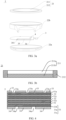
- FIG. 1 is a schematic structural diagram of an electronic device 100 according to some embodiments of this application.
- the electronic device 100 is a watch or a bracelet.
- the following embodiments are all described by using an example that the electronic device 100 is a watch, but this should not be construed as a limitation on this application.
- FIG. 1 and the following related drawings only schematically show some components included in the electronic device 100, and actual shapes, actual sizes, actual positions, and actual structures of the components are not defined by FIG. 1 and the following drawings.
- an XYZ coordinate system is established. Specifically, a width direction of the electronic device 100 is defined as an X-axis direction, a length direction of the electronic device 100 is defined as a Y-axis direction, and a thickness direction of the electronic device 100 is defined as a Z-axis direction. It may be understood that the coordinate system of the electronic device 100 may be flexibly set according to actual requirements. This is not specifically limited herein.
- the electronic device 100 includes a main body 2 and a watchband 1.
- the watchband 1 may include a first watchband 11 and a second watchband 12.
- the first watchband 11 and the second watchband 12 may be arranged on two opposite sides of the main body 2 along the Y-axis direction.
- a first locking portion 111 is arranged on the first watchband 11, and a second locking portion 121 is arranged on the second watchband 12.
- the first locking portion 111 and the second locking portion 121 are detachably locked to each other, so that the electronic device 100 can be worn on a wrist of a user.
- the mating structure of the first locking portion 111 and the second locking portion 121 may be a buckle structure such as a hook buckle, a concealed buckle, a butterfly buckle, a belt buckle, a foldable safety buckle, a foldable buckle, or a pin buckle. This is not specifically limited in this application.
- FIG. 2 is a perspective view of the main body 2 of the electronic device 100 according to an embodiment of this application
- FIG. 3a is an exploded view of the main body 2 of the electronic device 100 according to an embodiment of this application.
- the main body 2 may include a display module 21, a shell 22, a circuit board 3, a battery, and a temperature sensor 4.
- the electronic device 100 may not include the display module 21.
- the display module 21 includes a screen 211 and a decorative ring 212.
- the decorative ring 212 surrounds a periphery of the screen 211.
- the decorative ring 212 can protect and decorate the periphery of the screen 211.
- the screen 211 includes a light-transmissive cover plate 211a and a display 211b.
- the light-transmissive cover plate 211a and the display 211b are stacked and fixedly connected.
- the light-transmissive cover plate 211a is mainly configured to protect and prevent dust for the display 211b.
- a material of the light-transmissive cover plate 211a includes but is not limited to glass.
- the display 211b is configured to display images, videos, data, and the like.
- the display 211b may be a flexible display or a rigid display.
- the display 211b may be an organic light-emitting diode (organic light-emitting diode, OLED) display, an active-matrix organic light-emitting diode (active-matrix organic light-emitting diode, AMOLED) display, a mini light-emitting diode (mini organic light-emitting diode) display, a micro light-emitting diode (micro organic light-emitting diode) display, a micro organic light-emitting diode (micro organic light-emitting diode) display, a quantum dot light-emitting diode (quantum dot light emitting diodes, QLED) display, or a liquid crystal display (liquid crystal display, LCD).
- OLED organic light-emitting diode
- AMOLED active-matrix organic
- a shape of the screen 211 is not limited in this application.
- a display surface of the screen 211 may be circular or rectangular.
- shapes of other components such as the shell 22 and the decorative ring 212 of the main body 2 change with the shape of the screen 211.
- the following descriptions are made by using an example that the display surface of the screen 211 is circular.
- the shell 22 has an accommodating space therein.
- the shell 22 is configured to accommodate and protect the internal electronic components of the electronic device 100.
- the shell 22 may include a cover plate 22a and a side frame 22b, and the side frame 22b surrounds a periphery of the cover plate 22a.
- the cover plate 22a and the display 211b are stacked.
- the side frame 22b is arranged between a back cover and the display 211b, and the side frame 22b is fixed to the cover plate 22a.
- the side frame 22b may be fixedly connected to the cover plate 22a by an adhesive.
- the side frame 22b may alternatively be integrally formed with the cover plate 22a, that is, the side frame 22b and the cover plate 22a are an integral structure.
- the decorative ring 212 of the display module 21 is fixed to the side frame 22b.
- the decorative ring 212 may be fixed to the side frame 22b by an adhesive.
- the above accommodating space in the shell 22 may be defined by the screen 211, the cover plate 22a, and the side frame 22b.
- the accommodating space accommodates the circuit board 3, the temperature sensor 4, the battery, and the like.
- the circuit board 3 is a carrier configured to realize electrical connection of the electronic components.
- FIG. 4 is a cross-sectional view of the circuit board 3 of the electronic device 100 according to some embodiments of this application.
- the circuit board 3 includes a multi-layer wire structure formed by a metal layer 31 and insulating dielectric layers 32 that are alternately arranged in sequence.
- the multi-layer wire structure has a first surface and a second surface.
- the metal layer 31 of the multilayer wire structure includes a first metal layer 31a and a second metal layer 31b.
- the first metal layer 31a forms the first surface
- the second metal layer 31b forms the second surface.
- a first solder mask layer 33 is arranged on the first surface of the multi-layer wire structure, and a second solder mask layer 34 is arranged on the second surface of the multi-layer wire structure.
- the first solder mask layer 33 and the second solder mask layer 34 may be green ink, black ink, or the like. In a subsequent soldering process, the first solder mask layer 33 and the second solder mask layer 34 can prevent solder from being deposited on a surface of the circuit board 3.
- the metal layer 31 of the multi-layer wire structure may further include at least one intermediate metal layer 31c.
- the intermediate metal layer 31c is arranged between the first metal layer 31a and the second metal layer 31b.
- Signal lines may be arranged on the first metal layer 331a, the second metal layer 31b, and the intermediate metal layer 31c.
- the signal lines may include a positive wire 35 and a negative wire 36.
- the signal lines in the different metal layers 31 are connected through metallized vias.
- the first metal layer 31a, the second metal layer 31b, and the intermediate metal layer 31c may be copper foil layers.
- the wires on the first metal layer 31a, the second metal layer 31b, and the intermediate metal layer 31c may be formed by a lithography-and-etching process.
- the first solder mask layer 33 has first hollowed-out portions 33a
- the second solder mask layer 34 has second hollowed-out portions 34a.
- a part of the signal line on the first metal layer 31a may be exposed from the first hollowed-out portions 33a, so that components can be electrically connected to the signal line on the first metal layer 31a.
- a part of the signal line on the second metal layer 31b may be exposed from the second hollowed-out portions 34a, so that components can be electrically connected to the signal line on the second metal layer 31b.
- the circuit board 3 may be a rigid printed circuit, a flexible printed circuit, or a flexible-rigid printed circuit.
- the circuit board 3 may be an FR-4 dielectric board, a Rogers (Rogers) dielectric board, an FR-4 and Rogers mixed dielectric board, or the like.
- FR-4 herein is a mark of a flame-resistant material grade
- the Rogers dielectric board is a high-frequency board.
- a processor 301 may be arranged on the circuit board 3.
- the display 211 and the temperature sensor 4 are both electrically connected to the processor 301. In this way, the temperature detected by the temperature sensor 4 can be displayed on the display 211b after being processed by the processor.
- the battery is arranged in the accommodating space.
- the battery is configured to supply power to the electronic components such as the display 211b and the circuit board 3 in the electronic device 100.
- a battery mounting slot is provided in the shell 22, and the battery is mounted in the battery mounting slot.
- the temperature sensor 4 has a positive electrode 4a and a negative electrode 4b.
- the positive electrode 4a of the temperature sensor 4 is connected to the positive wire 35 of the circuit board 3
- the negative electrode 4b of the temperature sensor 4 is connected to the negative wire 36 of the circuit board 3
- the processor 301 is electrically connected to the positive wire 35 and the negative wire 36, so that electrical connection between the temperature sensor 4 and the processor 301 can be realized.
- the temperature sensor 4 and the processor 301 may be arranged on a same side surface of the circuit board 3. In some other embodiments, referring to FIG. 4b , the temperature sensor 4 and the processor 301 may be arranged on two opposite side surfaces of the circuit board 3 respectively.
- a contact member is arranged on the shell 22, and heat can be conducted between the temperature sensor 4 and the contact member. At least part of the surface of the contact member forms an outer surface of the electronic device 100. That is to say, at least part of the surface of the contact member is exposed from the shell 22.
- the part of the surface of the contact member forming the outer surface of the electronic device 100 may come into contact with the human skin, and the part of the surface may be formed as a contact surface.
- an area of the contact surface may be greater than or equal to 20 square millimeters, and the contact surface may be a flat surface or an arcuate surface, which may be specifically designed according to a physiological structure of a human body. In this way, the contact surface can come into contact with a user more effectively, thereby facilitating heat conduction.
- the contact member when the human skin comes into contact with the contact member, the contact member can absorb a temperature of the human skin and transfer the temperature of the human skin to the temperature sensor 4, so that the temperature of the human body can be detected by the temperature sensor 4. In this way, a health status of the user can be conveniently monitored through the electronic device 100. Therefore, by arranging the contact member on the shell 22 and thermally conductively connecting the contact member to the temperature sensor 4, the temperature of the human body can be conveniently detected while the temperature sensor 4 is arranged in in the shell 22, thereby improving reliability of the temperature sensor 4.
- the contact member may be arranged on a cover plate 22a of the shell 22 or on a side frame 22b of the shell 22.
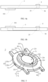
- FIG. 5 is a schematic structural diagram of a main body 2 of an electronic device 100 according to some other embodiments of this application
- FIG. 6 is an exploded view of the main body 2 of the electronic device 100 shown in FIG. 5 .
- the contact member is arranged on the cover plate 22a.
- An outer surface of the contact member and an outer surface of the cover plate 22a may be arranged on a same surface, or the outer surface of the contact member may protrude outward from the outer surface of the cover plate 22a. In this way, the contact member can conveniently come into contact with the human skin.
- a protruding portion 223 that protrudes away from a center of the accommodating space is arranged on the cover plate 22a, and the contact member is arranged on the protruding portion 223.
- the outer surface of the contact member and the outer surface of the protruding portion 223 may be arranged on a same plane. Therefore, the contact member can come into contact with a human skin, and an area of contact between the cover plate 22a of the electronic device 100 and a wrist skin can be increased when the electronic device 100 is worn on a wrist, thereby improving comfort of the electronic device 100.
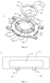
- FIG. 7 is a schematic diagram of the temperature sensor 4 according to some embodiments of this application.
- a temperature sensing element 42 of the temperature sensor 4 is usually packaged in an insulating housing 41, and the positive electrode 4a and the negative electrode 4b of the temperature sensor 4 are exposed from the insulating housing 41. Electrical connection between the temperature sensing element 42 and the circuit board 3 is realized by the positive electrode 4a and the negative electrode 4b of the temperature sensor 4. Therefore, during temperature measurement, after the contact member absorbs the temperature of the human skin, the temperature of the human skin is first transferred to the insulating housing 41 of the temperature sensor 4, and then is transferred to the temperature sensing element 42 through the insulating housing 41. Since heat conduction performance of the insulating housing 41 is relatively poor, a heat loss during heat conduction and a temperature transfer time are increased, thus reducing accuracy and sensitivity of the temperature measurement.
- FIG. 8 is a cross-sectional view along a line A-A in FIG. 5 .
- heat can be conducted between at least one of the positive wire 35 and the negative wire 36 of the circuit board 3 and the contact member, and the temperature sensor 4 is configured to perform temperature measurement according to the temperature transferred from the at least one of the positive wire 35 and the negative wire 36.
- heat can be conducted only between the positive wire 35 of the circuit board 3 and the contact member.
- the temperature sensor 4 may perform temperature measurement according to the temperature transferred by the positive wire 35.
- heat can be conducted only between the negative wire 36 of the circuit board 3 and the contact member.
- the temperature sensor 4 may perform temperature measurement according to the temperature transferred by the negative wire 36.
- heat can be conducted between the positive wire 35 of the circuit board 3 and the contact member and between the negative wire 36 of the circuit board 3 and the contact member.
- the temperature sensor 4 may perform temperature measurement according to the temperatures transferred by the positive wire 35 and the negative wire 36.
- the temperature of the contact member can be transferred to the positive electrode 4a of the temperature sensor 4 through the positive wire 35.
- the temperature sensor 4 can perform temperature measurement according to the temperature transferred to the positive electrode 4a of the temperature sensor 4.
- a heat conduction path between the contact member and the temperature sensor 4 is: contact member ⁇ positive wire 35 ⁇ positive electrode 4a of temperature sensor 4 ⁇ temperature sensing element 42 of temperature sensor 4.
- the temperature of the contact member can be transferred to the negative electrode 4b of the temperature sensor 4 through the negative wire 36.
- the temperature sensor 4 can perform temperature measurement according to the temperature transferred to the negative electrode 4b of the temperature sensor 4.
- a heat conduction path between the contact member and the temperature sensor 4 is: contact member-negative wire 36 ⁇ negative electrode 4b of temperature sensor 4 ⁇ temperature sensing element 42 of temperature sensor 4.
- the human skin heat absorbed by the contact member can be transferred to the temperature sensing element 42 of the temperature sensor 4 through the at least one of the positive wire 35 and the negative wire 36. Since the positive wire 35, the negative wire 36, the positive electrode 4a of the temperature sensor 4, and the negative electrode 4b of the temperature sensor 4 are all made of conductive materials, heat conduction performance thereof is more desirable than that of the insulating housing 41.
- heat conduction is enabled between at least one of the positive wire 35 and the negative wire 36 of the circuit board 3 and the contact member, so that the temperature sensor 4 can perform temperature measurement according to the temperature transferred from the at least one of the positive wire 35 and the negative wire 36.
- the heat conduction efficiency of the heat transfer from the human skin to the temperature sensor 4 is improved, the temperature measurement time is shortened, the sensitivity of the temperature sensor 4 is enhanced, and the heat loss during the heat conduction is reduced, thereby improving the accuracy of the temperature measurement.
- the temperature sensor 4 is a digital temperature sensor.
- the temperature sensor 4 may be a CMOS digital temperature sensor.
- the digital temperature sensor is an ultra-small, ultra-precise, low-power, and low-voltage temperature sensor that does not require user calibration.
- the accuracy of the temperature measurement can be improved, and a space occupied by the temperature sensor 4 can be reduced, thereby facilitating lightening and thinning of the electronic device 100.
- power consumption of electronic device 100 can be reduced.
- a thermal conductivity k1 of the contact member satisfies: k1 ⁇ 15 W/m•K.
- the contact member may be a stainless steel member obtained by machining a stainless steel material.
- the contact member is a type 316 stainless steel member with a thermal conductivity of 16.2 W/m•K.
- this application is not limited thereto. Therefore, heat conduction performance of the contact member can be ensured, so that the temperature of the human skin can be quickly transferred to the contact member, and the temperature in the contact member can be quickly transferred to the temperature sensor 4 for detection. In this way, the temperature transfer time is shortened, thereby shortening a temperature detection time, and improving the detection sensitivity of the temperature sensor 4.
- the electronic device 100 further includes a thermal insulator 6, and the thermal insulator 6 is wrapped around at least part of the outer surface of the temperature sensor 4. That is to say, the thermal insulator 6 may be wrapped around a part of the outer surface of the temperature sensor 4, or may be wrapped around an entire outer surface of the temperature sensor 4.
- the thermal insulator 6 can separate the temperature sensor 4 from other components in the shell 22, so that heat exchange between the temperature sensor 4 and the outside can be reduced, thereby preventing heat generated by the other components in the shell 22 from affecting the temperature sensor 4. In this way, accuracy of a measurement of the temperature sensor 4 is improved.
- the thermal insulator 6 may be rock wool, fiberglass wool, foam, or the like.
- the thermal insulator 6 may be bonded to the outer surface of the temperature sensor 4.
- the thermal insulator 6 may be a thermally insulating paint, and the thermal insulating paint may be coated on the outer surface of the temperature sensor 4. It may be understood that, the material of the thermal insulator 6 is not specifically limited in this application, as long as the thermal insulator 6 can insulate heat.
- the positive electrode 4a and the negative electrode 4b of the temperature sensor 4 are connected to the circuit board 3 by pads.
- FIG. 9a is a schematic diagram of connection between the temperature sensor 4 and the circuit board 3 according to some embodiments of this application
- FIG. 9b is a schematic diagram of a temperature transfer path during temperature measurement by the temperature sensor according to some embodiments of this application. Arrows in FIG. 9b indicate a temperature transfer direction.
- a positive welding leg 401 is arranged on the positive electrode 4a of the temperature sensor 4
- a negative welding leg 402 is arranged on the negative electrode 4b of the temperature sensor 4.
- the positive wire 35 includes a positive wire body 35a, a first metallized via 35b, and a first positive pad 35c.
- the positive wire body 35a is formed on the metal layer 31.
- the first metallized via 35b is provided in the circuit board 3.
- the first metallized via 35b extends through the two opposite side surfaces of the circuit board 3.
- the positive wire body 35a is electrically connected to the first metallized via 35b, and the first positive pad 35c is arranged on an end of the first metallized via 35b.
- the positive welding leg 401 of the temperature sensor 4 is electrically connected to the first positive pad 36c to realize electrical connection between the temperature sensor 4 and the positive wire 35.
- the negative wire 36 includes a negative wire body 36a, a second metallized via 36b, and a first negative pad 36c.
- the negative wire 36a is formed on the metal layer 31, and the second metallized via 36b is provided in the circuit board 3 and extends through the circuit board 3 along a thickness direction of the circuit board 3.
- the negative wire body 36a is electrically connected to the second metallized via 36b.
- the first negative pad 36c is arranged on an end of the second metallized via 36b.
- the first negative pad 36c forms the outer surface of the circuit board 3.
- the negative welding leg 402 of the temperature sensor 4 is electrically connected to the first negative pad 36c to realize electrical connection between the temperature sensor 4 and the negative wire 36. In this way, the electrical connection between the temperature sensor 4 and the positive wire 35 and the negative wire 36 of the circuit board 3 can be easily realized.
- the human skin heat absorbed by the contact member can be transferred to the positive electrode 4a of the temperature sensor 4 and/or the negative electrode 4b of the temperature sensor 4 through at least one of the first positive pad 35c and the first negative pad 36c, and then is transferred to the temperature sensing element 42 of the temperature sensor 4.
- the electrical connection between the temperature sensor 4 and the circuit board 3 can be easily realized, assembly difficulty is reduced, and the sensitivity of the temperature sensor 4 and the accuracy of the temperature measurement can be ensured.
- the positive wire 35 may not include the first positive pad 35c.
- the positive welding leg 401 of the temperature sensor 4 may be electrically connected to the first metallized via 35b to realize the electrical connection between the temperature sensor 4 and the positive wire 35.
- the negative wire 36 may not include the first negative pad 36c.
- the negative welding leg 402 of the temperature sensor 4 may be electrically connected to the second metallized via 36b to realize the electrical connection between the temperature sensor 4 and the negative wire 36. In this way, the electrical connection between the temperature sensor 4 and the positive wire 35 and the negative wire 36 can also be realized, and the structure of the electronic device 100 can be simplified.
- the contact member and temperature sensor 4 are arranged on the two opposite sides of the circuit board 3. Referring to FIG. 9a and FIG. 9b , the temperature sensor 4 is arranged on a side of the circuit board 3 facing away from the contact member.
- the positive wire 35 further includes a second positive pad 35d
- the negative wire 36 further includes a second negative pad 36d.
- the second positive pad 35d and the second negative pad 36d are arranged on a side surface of the circuit board 3 facing away from the temperature sensor 4, the second positive pad 35d and the first positive pad 35c are arranged on two ends of the first metallized via 35b opposite to each other, and the second negative pad 36d and the first negative pad 36c are arranged on two ends of the second metallized via 36b opposite to each other.
- the contact member may be thermally conductively connected to the second positive pad 35d to realize heat conduction between the contact member and the positive wire 35, and/or the contact member may be thermally conductively connected to the second negative pad 36d to realize heat conduction between the contact member and the negative wire 36. In this way, the temperature in the contact member can be transferred to the temperature sensing element 42 of the temperature sensor 4.
- thermally conductive connection between the at least one of the positive wire 35 and the negative wire 36 and the contact member can be realized.
- a gap between the contact member and the positive wire 35 and/or the negative wire 36 can be further reduced, thereby facilitating the heat conduction between the contact member and the positive wire 35 and/or the negative wire 36, reducing assembly difficulty, and realizing a more proper layout of an internal structure of the electronic device 100. Therefore, the structure of the electronic device 100 is more compact, thereby facilitating lightening and thinning of the electronic device 100.
- the positive wire 35 may not include the second positive pad 35d, and the negative wire may not include the second negative pad 36d.
- the contact member may be directly thermally conductively connected to at least one of the first metallized via 35b and the second metallized via 36b, so as to realize the heat conduction between the contact member and the positive wire 35 and/or the negative wire 36. In this way, the temperature in the contact member can be transferred to the temperature sensing element 42 of the temperature sensor 4. In this way, the heat conduction between the contact member and the positive wire 35 and/or the negative wire 36 can be realized, and the structure of the electronic device 100 can be simplified.
- the electronic device 100 further includes an insulating and thermally conductive member 5, and at least one of the positive wire 35 and the negative wire 36 is thermally conductively connected to the contact member by the insulating and thermally conductive member 5.
- the insulating and thermally conductive member 5 may cover a side surface of the contact member close to the circuit board 3.
- a thermal conductivity k2 of the insulating and thermally conductive member 5 satisfies: k2 ⁇ 10 W/m•K.
- the insulating and thermally conductive member 5 may be thermally conductive silicone, thermally conductive silicone grease, thermally conductive adhesive, or the like.
- the insulating and thermally conductive member 5 when heat conduction is enabled between the positive wire 35 and the contact member, the insulating and thermally conductive member 5 may be arranged between the positive wire 35 and the contact member. When heat conduction is enabled between the negative wire 36 and the contact member, the insulating and thermally conductive member 5 may be arranged between the negative wire 36 and the contact member. For example, in an example in FIG. 9a , the insulating and thermally conductive member 5 may cover the second positive pad 35d and the second negative pad 36d. In this way, the temperature in the contact member can be transferred to the positive wire 35 and/or the negative wire 36 through the insulating and thermally conductive member 5.
- the heat can be transferred more effectively, and heat dissipation can be reduced.
- the contact member can still be prevented from being electrified, thereby ensuring use safety of the electronic device 100.
- the electronic device includes a charging electrode 8 and a detection electrode 7 configured to detect vital sign information.
- the charging electrode 8 and the detection electrode 7 are arranged on the shell 22. At least part of a surface of the charging electrode 8 and at least part of a surface of the detection electrode 7 form the outer surface of the electronic device 100, and at least one of the charging electrode 8 and the detection electrode 7 forms the contact member. That is to say, the charging electrode 8 forms the contact member, the detection electrode 7 forms the contact member, or both the charging electrode 8 and the detection electrode 7 form the contact member.
- the charging electrode 8 may be electrically connected to the battery of the electronic device 100, so that when the charging electrode 8 is connected to an external power supply, the battery can be charged by the charging electrode 8.
- the charging electrode 8 includes a positive electrode 81 and a negative electrode 82.
- the positive electrode 81 and the negative electrode 82 both may be formed as a cylindrical structure, but this application is not limited thereto.
- a first via 224 and a second via 225 are arranged on the shell 22.
- the positive electrode 81 is inserted into the first via 224, and the negative electrode 82 is inserted into the second via 225.
- An outer surface of the positive electrode 81 and an outer surface of the negative electrode 82 both form the outer surface of the electronic device 100. This facilitates contact of the charging electrode 8 with the external power supply, and facilitates electrical connection between the positive electrode 81 and the negative electrode 82 and the battery.
- the contact member is the charging electrode 8
- one of the positive electrode 81 and the negative electrode 82 may be used as the contact member for heat conduction with the temperature sensor 4.
- both the positive electrode 81 and the negative electrode 82 may be used as the contact member for heat conduction with the temperature sensor 4, so that the area of contact between the contact member and the human skin can be increased.
- the detection electrode 7 configured to detect the vital sign information may be configured to detect vital sign information of the human body.
- the detection electrode 7 may be electrically connected to the processor 301. After the detection electrode 7 detects vital sign information of a user, the vital sign information is processed by the processor and then displayed on the display 211b. In this way, the vital sign information of the user can be conveniently detected, so that a health status of the user can be conveniently monitored.
- the detection electrode 7 may be an electrocardiogram (electro cardio gram, ECG) electrode.
- ECG electrocardiogram
- Detection data of the ECG electrode is generated according to an electrical signal of the human skin acquired by the ECG electrode.
- the detection data of the ECG electrode is used for representing a potential difference between two limbs of the human body, for example, between a left upper limb and a right upper limb, between a left lower limb and the right upper limb, or between the left lower limb and the left upper limb.
- the detection electrode 7 Since the detection electrode 7 has a relatively large area, using the detection electrode 7 as the contact member of the temperature sensor 4 can increase the area of contact between the contact member and the human skin, thereby improving the heat conduction efficiency between the contact member and the temperature sensor 4, and reducing a measurement error.
- the contact member for heat conduction with the temperature sensor 4 is not required to be additionally arranged when the electronic device 100 is provided with the charging electrode 8 or the detection electrode 7.
- a space occupied by the contact member is saved, thereby saving a space occupied in an overall design space of the electronic device 100. Therefore, more detection devices can be integrated on the electronic device 100 without increasing an area of the cover plate 22a, so that functions of the electronic device 100 are enriched. Moreover, holes required on the shell 22 can be reduced, thereby improving waterproof performance of the electronic device 100.
- an impedance Z of the contact member satisfies: Z ⁇ 1 ⁇ . Resistance to a current in a circuit with a resistance, an inductance, and a capacitance is referred to as an impedance.
- the contact member may be a stainless steel member, a copper member, or the like.
- the impedance of the contact member by setting the impedance of the contact member to be less than 1 S2, when the contact member is the charging electrode 8 or the detection electrode 7, it is ensured that the temperature of the human skin can be quickly transferred to the temperature sensor 4, the sensitivity of the temperature sensor 4 and the accuracy of temperature measurement are improved, and signals of excellent quality of the charging electrode 8 or the detection electrode 7 are ensured.
- the detection electrode 7 includes a first electrode 71 and a second electrode 72.
- the first electrode 71 and the second electrode 72 are both arranged on the shell 22 and are spaced apart from each other. At least part of the first electrode 71 and at least part of the second electrode 72 are exposed from shell 22, and the part of the first electrode 71 exposed from shell 22 and the part of the second electrode 72 exposed from shell 22 define an annular structure. Since the first electrode 71 and the second electrode 72 are spaced apart from each other, the annular structure is a discontinuous annular structure with discontinuous parts.
- the annular structure may be a square annular shape, a circular annular shape, an elliptical annular shape, or the like.
- the first electrode 71 and the second electrode 72 are both formed as an arcuate shape, and the first electrode 71 and the second electrode 72 are formed as a circular annular structure.
- the first electrode 71 and the second electrode 72 are arranged as an annular structure, an area of contact between the first electrode 71 and the second electrode 72 and the human body can be increased.
- the annular structure can improve stability of the contact between the detection electrode 7 and the human body, thereby improving accuracy of a detection result of the detection electrode 7.
- the detection electrode 7 is an ECG electrode, that is, the first electrode 71 and the second electrode 72 are both the ECG electrode, if the first electrode 71 and the second electrode 72 are spaced apart from each other, common mode rejection (common mode rejection, CMR) performance of the ECG electrode can be improved. Therefore, anti-interference performance of the ECG electrode is improved, so that signal quality of the ECG electrode is further improved, and the detection result is more accurate.
- the common mode rejection means offsetting common mode signals on any two ends (input points of the two ends have a same phase) and amplifying a differential mode signal (a potential difference between the two ends).
- the detection electrode 7 further includes a third electrode 73.
- the third electrode is the ECG electrode.
- the third electrode 73 may be arranged on the side frame 22b or the decorative ring 212. It may be understood that the first electrode 71 may be a positive ECG electrode, the second electrode 72 may be a driving electrode, and the third electrode 72 may be a negative ECG electrode.
- the first electrode 71 is the positive ECG electrode and the third electrode 72 is the negative ECG electrode
- a skin of the wrist comes into contact with the cover plate 22a of the electronic device 100 to come into contact with the positive ECG electrode
- an other hand presses the side frame 22b or the decorative ring 212 to come into contact with the negative ECG electrode, so that a loop is formed between the human body and the electronic device 100.
- ECG detection data can be acquired.
- the left hand can come into contact with the positive ECG electrode, and the right hand can come into contact with the negative ECG electrode, so that a loop is formed between the human body and the electronic device 100.
- an electrical signal representing the potential difference between the left upper limb and the right upper limb can be acquired.
- the first electrode 71 includes a first body portion 711 and a first protruding portion 712, and the first protruding portion 712 is arranged on an inner surface of the first body portion 711.
- the second electrode 72 includes a second body portion 721 and a second protruding portion 722, and the second protruding portion 722 is arranged on an inner surface of the second body portion 721.
- the "inner surface" of the first body portion 711 is a side surface of the first body portion 711 facing the accommodating space.
- the “inner surface” of the second body portion 721 is a side surface of the second body portion 721 facing the accommodating space.
- a first embedding groove 221 and a second embedding groove 222 are provided on an outer surface of the cover plate 22a.
- the first embedding groove 221 has a first communication hole 221a in communication with the accommodating space
- the second embedding groove 222 has a second communication hole 222a in communication with the accommodating space.
- the first body portion 711 of the first electrode 71 is arranged in the first embedding groove 221, and the first protruding portion 712 of the first electrode 71 extends into the accommodating space through the first communication hole 221a.
- the second body portion 721 of the second electrode 72 is arranged in the second embedding groove 222, and the second protruding portion 722 of the second electrode 72 extends into the accommodating space through the second communication hole 222a.
- the first electrode 71 and the second electrode 72 can be conveniently assembled on the shell 22, and the positions of the first electrode 71 and the second electrode 72 are more stable.
- the first communication hole 221a in the first embedding groove 221 and the second communication hole 222a in the second embedding groove 222 electrical connection between the first electrode 71 and the second electrode 72 and the circuit board 3 can be conveniently realized.
- first electrode 71 and the second electrode 72 are arranged axisymmetrically with respect to a central axis of the main body 2 in the X-axis direction or a central axis in the Y-axis direction. In this way, the first electrode 71 and the second electrode 72 can be distributed more uniformly, thereby further enhancing stability of the contact between the detection electrode 7 and the user, so that the detection result is more accurate. In addition, an appearance of the electronic device 100 is improved.
- the positive electrode 81 and the negative electrode 82 of the charging electrode 8 are arranged on an extending path of the annular structure or an extended line of the extending path.
- the space of the shell 22 can be properly used, so that the overall layout of the electronic device 100 is more proper. Therefore, the charging electrode 8 and the detection electrode 7 both can be integrated on the shell 22, so that the functions of the electronic device 100 are more abundant and diverse.
- the first electrode 71 has a first end 71a and a second end 71b
- the second electrode 72 has a third end 72a and a fourth end 72b.
- the first end 71a of the first electrode 71 and the third end 72a of the second electrode 72 are opposite to and spaced apart from each other to form a first spacer region 226, and the second end 71b of the first electrode 71 and the fourth end 72b of the second electrode 72 are opposite to and spaced apart from each other to form a second spacer region 227.
- the first spacer region 226 and the second spacer region 227 are arranged on the extended line of the above extending path.
- One of the positive electrode 81 and the negative electrode 82 of the charging electrode 8 may be arranged in the first spacer region 226, and the other of the positive electrode 81 and the negative electrode 82 of the charging electrode 8 may be arranged in the second spacer region 227.
- the positive electrode 81 and the negative electrode 82 of the charging electrode 8 both may be arranged in the first spacer region 226 or the second spacer region 227. Therefore, a space between the first electrode 71 and the second electrode 72 can be fully used to arrange the charging electrode 8, so that the space of the shell 22 is fully and properly used, and a machining process of the first electrode 71 and the second electrode 72 is simplified, thereby improving machining efficiency.
- FIG. 10 is a perspective view of a main body 2 of an electronic device 100 according to some other embodiments of this application.
- a difference between a structure of the main body 2 of the electronic device 100 shown in FIG. 10 and the main body 2 of the electronic device 100 shown in FIG. 5 is that in the example of FIG. 10 , the positive electrode 81 and the negative electrode 82 are arranged on the extending path of the annular structure.
- a first avoidance hole 71c is provided on the first electrode 71
- a second avoidance hole 72c is provided on the second electrode 72, so that the positive electrode 81 and the negative electrode 82 can be respectively arranged in the first avoidance hole 71c and the second avoidance hole 72c.
- the space of the shell 22 can be properly used, so that the overall layout of the electronic device 100 is more proper. Therefore, the charging electrode 8 and the detection electrode 7 both can be integrated on the shell 22, so that the functions of the electronic device 100 are more abundant and diverse.
- the electronic device 100 further includes a photoplethysmography (photo plethysmo graphy, PPG) detection device, and a detection light window 228 of the PPG detection device is arranged on an inner side of the annular structure.
- the PPG detection device is configured to detect a PPG signal of a to-be-tested object, and can obtain health data such as a pulse of the to-be-tested object.
- the detection light window 228 is a light-transmissive formed on the shell 22.
- light-transmissive glass may be arranged on the inner side of the annular structure to form the detection light window 228.
- Light emitted by the PPG detection device can be irradiated to a surface of the human skin through the detection light window 228, and reflected light after the light irradiated on the surface of human skin is absorbed by human blood and a muscle tissue 400 and the is received by the PPG detection device through the detection light window 228.
- the PPG detection device is an infrared non-destructive detection technology, which detects, by using a photoelectric sensor, a different intensity of reflected light after absorption by human blood and a muscle tissue 400, and traces a variation of a blood vessel volume during a cardiac cycle, so as to obtain a pulse waveform and then calculate a heart rate.
- FIG. 11 is a schematic diagram of a detection process performed by the PPG detection device.
- the PPG detection device includes a light-emitting element 91 and a light detector 92.
- the light-emitting element 91 and the light detector 92 may be arranged in the accommodating space and are electrically connected to the processor, and the light-emitting element 91 and the light detector 92 are both opposite to the detection light window 228.
- the light-emitting element 91 when the light-emitting element 91 emits a light beam of a certain wavelength, the light beam can be irradiated to the surface of the human skin (for example, the wrist skin) through the detection light window 228.
- Contraction and expansion of blood vessels affect transmission or reflection of light during each heartbeat.
- the light passes through a skin tissue 200 and is reflected to the light detector 92 by the detection light window 228, the light attenuates to a certain extent.
- Absorption of light by a muscle tissue 400, bones, veins and other connecting tissues substantially does not vary (if there is no large movement of a to-be-measured site), but absorption of light by an artery 300 varies. This is because there is blood pulsation in the artery 300.
- the light absorption certainly varies. Therefore, after the light detector 92 converts an optical signal reflected and/or transmitted by a human body to an electrical signal, since the absorption of the light signal by the artery 300 varies and the absorption of the light signal by the other tissues substantially does not vary, the obtained signals may be classified into a direct current DC signal and an alternating current AC signal. By extracting the AC signal, characteristics of blood flowing can be learned, so that the pulse waveform can be obtained, and the heart rate can be calculated. It may be understood that a blood pressure value may be further calculated by using the detection data of the PPG detection device and the detection data of the ECG electrode 73.
- the detection light window 228 of the PPG detection device By arranging the detection light window 228 of the PPG detection device on the inner side of the above annular structure, the space of the shell 22 can be properly used, so that the overall structure of the electronic device 100 is more compact. Therefore, the detection light window 228 of the PPG detection device, the ECG electrode 73, the charging electrode 8, and the contact member of the temperature sensor 4 can all be integrated on the cover plate 22a of the electronic device 100 without increasing the area of the cover plate 22a, so that the electronic device 100 can synchronously detect PPG detection data, ECG detection data, and body temperature detection data of a user, thereby obtaining data of the user reflecting a health status, such as a pulse, a heart rate, a blood pressure, and an electrocardiogram. In addition, the electronic device can determine emotion and tension of the user according to the ECG detection data and the body temperature detection data, thereby monitoring the health status of the user more comprehensively.
- an area of the detection light window 228 is substantially the same as an area of the inner side of the annular structure. In this way, a detection area of the detection light window 228 can be increased, thereby ensuring that the light of the PPG detection device is not blocked, and improving detection accuracy of the PPG detection device.
- the electronic device 100 provided in this application may be worn on a wrist, or may be placed on a forehead, an armpit, or the like, and comes into contact with a human skin by using a contact member, so as to realize temperature detection of the human body.
- a body temperature may be detected in real time by the electronic device 100.
- the body temperature may be detected at a predetermined interval to monitor the body temperature in real time.
- the above predetermined time may be 1 min, 3 min, 5 min, 10 min, 30 min, 60 min, or the like.
- the user may adjust the predetermined time according to actual requirements. This is not limited in this application.
- the user may manually activate a temperature detection function by triggering a start switch, to realize detection of the temperature of the human body.
Landscapes
- Health & Medical Sciences (AREA)
- Life Sciences & Earth Sciences (AREA)
- Engineering & Computer Science (AREA)
- Physics & Mathematics (AREA)
- Cardiology (AREA)
- Molecular Biology (AREA)
- Animal Behavior & Ethology (AREA)
- Biomedical Technology (AREA)
- Heart & Thoracic Surgery (AREA)
- Medical Informatics (AREA)
- Biophysics (AREA)
- Surgery (AREA)
- Pathology (AREA)
- General Health & Medical Sciences (AREA)
- Public Health (AREA)
- Veterinary Medicine (AREA)
- Physiology (AREA)
- Microelectronics & Electronic Packaging (AREA)
- Pulmonology (AREA)
- General Physics & Mathematics (AREA)
- Measuring And Recording Apparatus For Diagnosis (AREA)
Abstract
Description
- This application claims priority to
Chinese Patent Application No. 202122038383.X, filed with the China National Intellectual Property Administration on August 26, 2021 - This application relates to the technical field of electronic devices, and in particular, to an electronic device.
- As living standards improve, people attach increasing importance to their health statuses. In order to help people learn their health statuses, increasing electronic devices such as watches and bracelets are configured with a health monitoring function, such as temperature measurement. However, accuracy of temperature measurement by current electronic devices is low.
- This application provides an electronic device, to improve measurement accuracy of a temperature sensor, shorten a measurement time of the temperature sensor, and improve sensitivity of the temperature sensor.
- To achieve the above purpose, embodiments of this application adopt the following technical solutions:
- This application provides an electronic device. The electronic device includes a shell, a contact member, a temperature sensor, and a circuit board. The shell has an accommodating space. The contact member is arranged on the shell, and at least part of a surface of the contact member forms an outer surface of the electronic device. That is to say, a part of the surface of the contact member forms the outer surface of the electronic device, or an entire surface of the contact member forms the outer surface of the electronic device. The temperature sensor is arranged in the accommodating space and has a positive electrode and a negative electrode. The circuit board is arranged in the accommodating space and provided with a positive wire and a negative wire. The positive wire is connected to the positive electrode of the temperature sensor. The negative wire is connected to the negative electrode of the temperature sensor. At least one of the positive wire and the negative wire is thermally conductively connected to the contact member. The temperature sensor is configured to perform temperature measurement according to a temperature transferred from the at least one of the positive wire and the negative wire.
- According to the electronic device provided in this application, heat conduction is enabled between at least one of the positive wire and the negative wire of the circuit board and the contact member, so that the temperature sensor can perform temperature measurement according to the temperature transferred from the at least one of the positive wire and the negative wire. In this way, heat conduction efficiency of heat transfer from a human skin to the temperature sensor is improved, a temperature measurement time is shortened, sensitivity of the temperature sensor is enhanced, and a heat loss during the heat conduction is reduced, thereby improving accuracy of temperature measurement.
- In a possible implementation, a thermal conductivity k1 of the contact member satisfies: k1≥15 W/m-K. Therefore, heat conduction performance of the contact member can be ensured, so that a temperature of the human skin can be quickly transferred to the contact member, and the temperature in the contact member can be quickly transferred to the temperature sensor for detection. In this way, a temperature transfer time is shortened, thereby shortening a temperature detection time, and improving the detection sensitivity of the temperature sensor.
- In a possible implementation, the electronic device further includes an insulating and thermally conductive member, and the at least one of the positive wire and the negative wire is thermally conductively connected to the contact member by the insulating and thermally conductive member. In this way, the temperature in the contact member can be transferred to the positive wire and/or the negative wire through the insulating and thermally conductive member. Compared with a solution in which the contact member is directly connected to the positive wire and/or the negative wire, in the solution of the embodiments of this application, the heat can be transferred more effectively, and heat dissipation can be reduced. In addition, even if the contact member is a conductive member, the contact member can still be prevented from being electrified, thereby ensuring use safety of the electronic device.
- In a possible implementation, a thermal conductivity k2 of the insulating and thermally conductive member satisfies: k2≥10 W/m•K. Therefore, the heat conduction performance of the insulating and thermally conductive member can be ensured, so that the temperature in the contact member can be quickly transferred to the temperature sensor for detection.
- In a possible implementation, the electronic device further includes a thermal insulator wrapped around at least part of an outer surface of the temperature sensor. The thermal insulator may be wrapped around a part of the outer surface of the temperature sensor, or may be wrapped around an entire outer surface of the temperature sensor. The thermal insulator can separate the temperature sensor from other components on the circuit board, so that heat exchange between the temperature sensor and the outside can be reduced, thereby preventing heat generated by the other components on the circuit board from affecting the temperature sensor. In this way, accuracy of a measurement of the temperature sensor is improved.
- In a possible implementation, the contact member and the temperature sensor are arranged on two opposite sides of the circuit board. By arranging the contact member and the temperature sensor on the two opposite sides of the circuit board, a gap between the contact member and the positive wire and/or the negative wire is reduced, thereby facilitating the heat conduction between the contact member and the positive wire and/or the negative wire, reducing assembly difficulty, and realizing a more proper layout of an internal structure of the electronic device. Therefore, the structure of the electronic device is more compact, thereby facilitating lightening and thinning of the electronic device.
- In a possible implementation, the circuit board includes a multi-layer wire structure formed by a metal layer and insulating dielectric layers that are alternately arranged in sequence. The positive wire includes a positive wire body and a first metallized via, the positive wire body is formed on the metal layer, the first metallized via extends through surfaces on the two opposite sides of the circuit board, and the positive wire body is electrically connected to the first metallized via. The negative wire includes a negative wire body and a second metallized via, the negative wire body is formed on the metal layer, the second metallized via extends through the surfaces on the two opposite sides of the circuit board, and the negative wire body is electrically connected to the second metallized via. At least one of the first metallized via and the second metallized via is thermally conductively connected to the contact member. In this way, the at least one of the positive wire and the negative wire can be thermally conductively connected to the contact member conveniently, and the structure of the electronic device can be simplified.
- In a possible implementation, the positive wire further includes a first positive pad and a second positive pad arranged opposite to each other on two ends of the first metallized via, and the first positive pad is electrically connected to the positive electrode of the temperature sensor. The negative wire further includes a first negative pad and a second negative pad arranged opposite to each other on one end of the second metallized via, and the first negative pad is electrically connected to the negative electrode of the temperature sensor. At least one of the second positive pad and the second negative pad is thermally conductively connected to the contact member.
- In this way, the at least one of the positive wire and the negative wire can be thermally conductively connected to the contact member conveniently. In addition, by arranging the contact member and the temperature sensor on the two opposite sides of the circuit board, a gap between the contact member and the positive wire and/or the negative wire can be further reduced, thereby facilitating the heat conduction between the contact member and the positive wire and/or the negative wire, reducing assembly difficulty of assembly, and realizing a more proper layout of an internal structure of the electronic device. In this way, the structure of the electronic device is more compact, thereby facilitating lightening and thinning of the electronic device.
- In a possible implementation, the electronic device includes a charging electrode and a detection electrode configured to detect vital sign information, the charging electrode and the detection electrode are arranged on the shell, and at least part of a surface of the charging electrode (a part of the surface of the charging electrode or an entire surface of the charging electrode) and at least part of a surface of the detection electrode (a part of the surface of the detection electrode or an entire surface of the detection electrode) form the outer surface of the electronic device. At least one of the charging electrode and the detection electrode forms the contact member. Since the charging electrode or the detection electrode of the electronic device is used as the contact member of the temperature sensor, and the temperature of the human skin is transferred to the temperature sensor through the charging electrode or the detection electrode, the contact member for heat conduction with the temperature sensor is not required to be additionally arranged when the electronic device is provided with the charging electrode or the detection electrode. In this way, a space occupied by the contact member is saved, thereby saving a space occupied in an overall design space of the electronic device. Therefore, more detection devices can be integrated on the electronic device without increasing an area of the cover plate, so that functions of the electronic device are enriched. Moreover, holes required on the shell can be reduced, thereby improving waterproof performance of the electronic device.
- In a possible implementation, an impedance Z of the contact member satisfies: Z≤1 Ω. In this embodiment, by setting the impedance of the contact member to be less than 1 S2, when the contact member is the charging electrode or the detection electrode, it is ensured that the temperature of the human skin can be quickly transferred to the temperature sensor, the sensitivity of the temperature sensor and the accuracy of temperature measurement are improved, and signals of excellent quality of the charging electrode or the detection electrode are ensured.
- In a possible implementation, the detection electrode is configured to detect an electrocardiogram electrode of an electrocardiogram. In this way, electrocardiogram information of a user can be easily obtained, thereby facilitating monitoring of a health status of the user.
- In a possible implementation, the detection electrode includes a first electrode and a second electrode, the first electrode and the second electrode are both arranged on the shell and are spaced apart from each other, at least part of the first electrode and at least part of the second electrode are exposed from the shell, and the part of the first electrode exposed from the shell and the part of the second electrode exposed from the shell define an annular structure. In this way, an area of contact between the first electrode and the second electrode and a human body can be increased. In addition, the annular structure can improve stability of the contact between the detection electrode and the human body, thereby improving accuracy of a detection result of the detection electrode. In addition, when the detection electrode is an ECG electrode, that is, the first electrode and the second electrode are both the ECG electrode, if the first electrode and the second electrode are spaced apart from each other, common mode rejection (common mode rejection, CMR) performance of the ECG electrode can be improved. Therefore, anti-interference performance of the ECG electrode is improved, so that signal quality of the ECG electrode is further improved, and the detection result is more accurate.
- In a possible implementation, the charging electrode includes a positive electrode and a negative electrode arranged on an extending path of the annular structure or on an extended line of the extending path. Therefore, a space of the shell can be properly used, so that the overall layout of the electronic device is more proper, and the charging electrode and the detection electrode can be integrated on the shell, so that the functions of the electronic device are more diverse.
- In a possible implementation, the electronic device further includes a photoplethysmography detection device, where a detection light window of the photoplethysmography detection device is arranged on an inner side of the annular structure. In this way, the space of the shell can be properly used, so that the overall structure of the electronic device is more compact. Therefore, the detection light window of the photoplethysmography detection device, the ECG electrode, the charging electrode, and the contact member of the temperature sensor can all be integrated on the cover plate of the electronic device without increasing the area of the cover plate, so that the electronic device can simultaneously detect PPG detection data, ECG detection data, and body temperature detection data of a user, thereby obtaining data of the user reflecting a health status, such as a pulse, a heart rate, a blood pressure, and an electrocardiogram. In addition, the electronic device can determine emotion and tension of the user according to the ECG detection data and the body temperature detection data, thereby monitoring the health status of the user more comprehensively.
- In a possible implementation, an area of the detection light window is substantially the same as an area of the inner side of the annular structure. In this way, the detection area of the detection light window can be increased, thereby ensuring that light of the PPG detection device is not blocked, and improving detection accuracy of the PPG detection device.
- In a possible implementation, the shell includes a cover plate and a side frame surrounding a periphery of the cover plate. A protruding portion protruding away from a center of the accommodating space is arranged on the cover plate, and the contact member is arranged on the protruding portion. Therefore, the contact member can come into contact with a human skin, and an area of contact between the cover plate of the electronic device and a wrist skin can be increased when the electronic device is worn on a wrist, thereby improving comfort of the electronic device.
- In a possible implementation, the temperature sensor is a digital temperature sensor. Therefore, the temperature measurement accuracy can be improved, and the space occupied by the temperature sensor can be reduced, thereby facilitating lightening and thinning of the electronic device. In addition, power consumption of electronic device can be reduced.
-
-
FIG. 1 is a schematic structural diagram of an electronic device according to some embodiments of this application; -
FIG. 2 is a schematic diagram of a main body of the electronic device according to an embodiment of this application; -
FIG. 3a is an exploded view of the main body of the electronic device according to an embodiment of this application; -
FIG. 3b is a cross-sectional view of a screen of the electronic device according to some embodiments of this application; -
FIG. 4 is a cross-sectional view of a circuit board of the electronic device according to some embodiments of this application; -
FIG. 4a is a schematic diagram of the circuit board of the electronic device according to some embodiments of this application; -
FIG. 4b is a schematic diagram of a circuit board of an electronic device according to some other embodiments of this application; -
FIG. 5 is a schematic structural diagram of a main body of an electronic device according to some other embodiments of this application; -
FIG. 6 is an exploded view of the main body of the electronic device shown inFIG. 5 ; -
FIG. 7 is a schematic structural diagram of a temperature sensor according to some other embodiments of this application; -
FIG. 8 is a cross-sectional view along a line A-A inFIG. 5 ; -
FIG. 9a is a schematic diagram of connection between a temperature sensor and a circuit board according to some embodiments of this application; -
FIG. 9b is a schematic diagram of a temperature transfer path during temperature measurement by the temperature sensor according to some embodiments of this application; -
FIG. 10 is a schematic structural diagram of a main body of an electronic device according to still other embodiments of this application; and -
FIG. 11 is a schematic diagram of a detection process performed by a PPG detection device according to some embodiments of this application. - Reference Numerals:
- 100. Electronic device
- 1. Watchband; 11: First watchband; 111. First locking portion; 12. Second watchband; 121. Second locking portion;
- 2. Main body;
- 21. Display module; 211. Screen; 211a. Light-transmissive cover plate; 211b. Display; 212. Decorative ring;
- 22. Shell;
- 22a. Cover plate; 221. First embedding groove; 221a. First communication hole; 222. Second embedding groove; 222a. Second communication hole; 223. Protruding portion; 224. First via; 225. Second via; 226. First spacer region; 227. Second spacer region; 228. Detection light window;
- 22b. Side frame;
- 3. Circuit board; 31. Metal layer; 31a. First metal layer; 31b. Second metal layer; 31c. Intermediate metal layer; 32. Insulating dielectric layer; 33. First solder mask layer; 33a. First hollowed-out portion; 34. Second solder mask layer; 34a. Second hollowed-out portion; 35. Positive wire; 35a. Positive wire body; 35b. First metallized via; 35c. First positive pad; 35d. Second positive pad; 36. Negative wire; 36a. Negative wire body; 36b. Second metallized via; 36c. First negative pad; 36d. Second negative pad;
- 301. Processor;
- 4. Temperature sensor; 4a. Positive electrode; 4b. Negative electrode; 401. Positive welding leg; 402. Negative welding leg; 41. Insulating housing; 42. Temperature sensing element;
- 5. Insulating and thermally conductive member;
- 6. Thermal insulator;
- 7. Detection electrode; 71. First electrode; 711. First body portion; 712. First protruding portion; 71a. First end; 71b. Second end; 71c. First avoidance hole; 72. Second electrode; 721. Second body portion; 722. Second protruding portion; 72a. Third end; 72b. Fourth end; 72c. Second avoidance hole; 73. ECG electrode;
- 8. Charging electrode; 81. Positive electrode; 82. Negative electrode;
- 91. Light-emitting element; 92. Light detector;
- 200. Skin tissue; 300. Artery; 400. Muscle tissue.
- In the embodiments of this application, terms "first", "second", "third", and "fourth" are used merely for the purpose of description, and shall not be construed as indicating or implying relative importance or implying a quantity of indicated technical features. Therefore, features defining "first", "second", "third", and "fourth" may explicitly or implicitly include one or more such features.
- In the embodiments of this application, the terms "include", "comprise", and any variants thereof are intended to cover a non-exclusive inclusion. Therefore, in the context of a process, method, object, or apparatus that includes a series of elements, the process, method, object, or apparatus not only includes such elements, but also includes other elements not specified expressly, or may include inherent elements of the process, method, object, or apparatus. Without more limitations, elements defined by the sentence "including one" does not exclude that there are still other same elements in the processes, methods, objects, or apparatuses.
- "And/or" in the embodiments of this application describes only an association relationship for describing associated objects and represents that three relationships may exist. For example, A and/or B may represent the following three cases: Only A exists, both A and B exist, and only B exists. In addition, the character "/" in this specification generally indicates an "or" relationship between the associated obj ects.
- This application provides an
electronic device 100. Theelectronic device 100 can detect a temperature of a human body to determine a health status of the human body. Specifically, in theelectronic device 100 provided in this application, atemperature sensor 4 configured to detect the temperature of the human body is arranged, and a positive wire and a negative wire of thetemperature sensor 4 are in contact with a contact member on ashell 22, so as to transfer the temperature of the human body to thetemperature sensor 4 through the contact member, the positive wire, and the negative wire in sequence for measurement, thereby ensuring accuracy and sensitivity of the temperature detection. - Specifically, the
electronic device 100 includes, but is not limited to a wearable device (for example, a watch, a wristband, and smartglasses), a phone, a tablet personal computer (tablet personal computer), a laptop computer (laptop computer), a personal digital assistant (personal digital assistant, PDA), a personal computer, a notebook (notebook), an in-vehicle device, and otherelectronic devices 100. - Referring to
FIG. 1, FIG. 1 is a schematic structural diagram of anelectronic device 100 according to some embodiments of this application. In this embodiment, theelectronic device 100 is a watch or a bracelet. For ease of description, the following embodiments are all described by using an example that theelectronic device 100 is a watch, but this should not be construed as a limitation on this application. - It may be understood that
FIG. 1 and the following related drawings only schematically show some components included in theelectronic device 100, and actual shapes, actual sizes, actual positions, and actual structures of the components are not defined byFIG. 1 and the following drawings. - In order to facilitate the description of the following embodiments, an XYZ coordinate system is established. Specifically, a width direction of the
electronic device 100 is defined as an X-axis direction, a length direction of theelectronic device 100 is defined as a Y-axis direction, and a thickness direction of theelectronic device 100 is defined as a Z-axis direction. It may be understood that the coordinate system of theelectronic device 100 may be flexibly set according to actual requirements. This is not specifically limited herein. - Specifically, referring to
FIG. 1 , theelectronic device 100 includes amain body 2 and awatchband 1. Thewatchband 1 may include afirst watchband 11 and asecond watchband 12. Thefirst watchband 11 and thesecond watchband 12 may be arranged on two opposite sides of themain body 2 along the Y-axis direction. Afirst locking portion 111 is arranged on thefirst watchband 11, and asecond locking portion 121 is arranged on thesecond watchband 12. Thefirst locking portion 111 and thesecond locking portion 121 are detachably locked to each other, so that theelectronic device 100 can be worn on a wrist of a user. It should be understood that the mating structure of thefirst locking portion 111 and thesecond locking portion 121 may be a buckle structure such as a hook buckle, a concealed buckle, a butterfly buckle, a belt buckle, a foldable safety buckle, a foldable buckle, or a pin buckle. This is not specifically limited in this application. - Referring to
FIG. 2 andFIG. 3a ,FIG. 2 is a perspective view of themain body 2 of theelectronic device 100 according to an embodiment of this application, andFIG. 3a is an exploded view of themain body 2 of theelectronic device 100 according to an embodiment of this application. Themain body 2 may include adisplay module 21, ashell 22, acircuit board 3, a battery, and atemperature sensor 4. In some other embodiments, theelectronic device 100 may not include thedisplay module 21. - Referring to
FIG. 3b , thedisplay module 21 includes ascreen 211 and adecorative ring 212. Thedecorative ring 212 surrounds a periphery of thescreen 211. Thedecorative ring 212 can protect and decorate the periphery of thescreen 211. Thescreen 211 includes a light-transmissive cover plate 211a and adisplay 211b. The light-transmissive cover plate 211a and thedisplay 211b are stacked and fixedly connected. The light-transmissive cover plate 211a is mainly configured to protect and prevent dust for thedisplay 211b. A material of the light-transmissive cover plate 211a includes but is not limited to glass. - The
display 211b is configured to display images, videos, data, and the like. Thedisplay 211b may be a flexible display or a rigid display. For example, thedisplay 211b may be an organic light-emitting diode (organic light-emitting diode, OLED) display, an active-matrix organic light-emitting diode (active-matrix organic light-emitting diode, AMOLED) display, a mini light-emitting diode (mini organic light-emitting diode) display, a micro light-emitting diode (micro organic light-emitting diode) display, a micro organic light-emitting diode (micro organic light-emitting diode) display, a quantum dot light-emitting diode (quantum dot light emitting diodes, QLED) display, or a liquid crystal display (liquid crystal display, LCD). - It should be noted that a shape of the
screen 211 is not limited in this application. A display surface of thescreen 211 may be circular or rectangular. When the shape of thescreen 211 changes, shapes of other components such as theshell 22 and thedecorative ring 212 of themain body 2 change with the shape of thescreen 211. For ease of description, the following descriptions are made by using an example that the display surface of thescreen 211 is circular. - The
shell 22 has an accommodating space therein. Theshell 22 is configured to accommodate and protect the internal electronic components of theelectronic device 100. Referring toFIG. 2 , theshell 22 may include acover plate 22a and aside frame 22b, and theside frame 22b surrounds a periphery of thecover plate 22a. Thecover plate 22a and thedisplay 211b are stacked. Theside frame 22b is arranged between a back cover and thedisplay 211b, and theside frame 22b is fixed to thecover plate 22a. Exemplarily, theside frame 22b may be fixedly connected to thecover plate 22a by an adhesive. Theside frame 22b may alternatively be integrally formed with thecover plate 22a, that is, theside frame 22b and thecover plate 22a are an integral structure. Thedecorative ring 212 of thedisplay module 21 is fixed to theside frame 22b. In some embodiments, thedecorative ring 212 may be fixed to theside frame 22b by an adhesive. The above accommodating space in theshell 22 may be defined by thescreen 211, thecover plate 22a, and theside frame 22b. The accommodating space accommodates thecircuit board 3, thetemperature sensor 4, the battery, and the like. - The
circuit board 3 is a carrier configured to realize electrical connection of the electronic components.FIG. 4 is a cross-sectional view of thecircuit board 3 of theelectronic device 100 according to some embodiments of this application. Referring toFIG. 4 , thecircuit board 3 includes a multi-layer wire structure formed by ametal layer 31 and insulatingdielectric layers 32 that are alternately arranged in sequence. The multi-layer wire structure has a first surface and a second surface. Themetal layer 31 of the multilayer wire structure includes afirst metal layer 31a and asecond metal layer 31b. Thefirst metal layer 31a forms the first surface, and thesecond metal layer 31b forms the second surface. A firstsolder mask layer 33 is arranged on the first surface of the multi-layer wire structure, and a secondsolder mask layer 34 is arranged on the second surface of the multi-layer wire structure. The firstsolder mask layer 33 and the secondsolder mask layer 34 may be green ink, black ink, or the like. In a subsequent soldering process, the firstsolder mask layer 33 and the secondsolder mask layer 34 can prevent solder from being deposited on a surface of thecircuit board 3. - Further, the
metal layer 31 of the multi-layer wire structure may further include at least oneintermediate metal layer 31c. Theintermediate metal layer 31c is arranged between thefirst metal layer 31a and thesecond metal layer 31b. Signal lines may be arranged on the first metal layer 331a, thesecond metal layer 31b, and theintermediate metal layer 31c. The signal lines may include apositive wire 35 and anegative wire 36. In thecircuit board 3, the signal lines in thedifferent metal layers 31 are connected through metallized vias. - In some embodiments, the
first metal layer 31a, thesecond metal layer 31b, and theintermediate metal layer 31c may be copper foil layers. The wires on thefirst metal layer 31a, thesecond metal layer 31b, and theintermediate metal layer 31c may be formed by a lithography-and-etching process. - Specifically, the first
solder mask layer 33 has first hollowed-outportions 33a, and the secondsolder mask layer 34 has second hollowed-outportions 34a. A part of the signal line on thefirst metal layer 31a may be exposed from the first hollowed-outportions 33a, so that components can be electrically connected to the signal line on thefirst metal layer 31a. A part of the signal line on thesecond metal layer 31b may be exposed from the second hollowed-outportions 34a, so that components can be electrically connected to the signal line on thesecond metal layer 31b. - It may be understood that the
circuit board 3 may be a rigid printed circuit, a flexible printed circuit, or a flexible-rigid printed circuit. Thecircuit board 3 may be an FR-4 dielectric board, a Rogers (Rogers) dielectric board, an FR-4 and Rogers mixed dielectric board, or the like. FR-4 herein is a mark of a flame-resistant material grade, and the Rogers dielectric board is a high-frequency board. - A
processor 301 may be arranged on thecircuit board 3. Thedisplay 211 and thetemperature sensor 4 are both electrically connected to theprocessor 301. In this way, the temperature detected by thetemperature sensor 4 can be displayed on thedisplay 211b after being processed by the processor. - The battery is arranged in the accommodating space. The battery is configured to supply power to the electronic components such as the
display 211b and thecircuit board 3 in theelectronic device 100. In some embodiments, a battery mounting slot is provided in theshell 22, and the battery is mounted in the battery mounting slot. - Specifically, referring to
FIG. 4a and FIG. 4b , thetemperature sensor 4 has apositive electrode 4a and anegative electrode 4b. Thepositive electrode 4a of thetemperature sensor 4 is connected to thepositive wire 35 of thecircuit board 3, thenegative electrode 4b of thetemperature sensor 4 is connected to thenegative wire 36 of thecircuit board 3, and theprocessor 301 is electrically connected to thepositive wire 35 and thenegative wire 36, so that electrical connection between thetemperature sensor 4 and theprocessor 301 can be realized. - In some embodiments, referring to
FIG. 4a , thetemperature sensor 4 and theprocessor 301 may be arranged on a same side surface of thecircuit board 3. In some other embodiments, referring toFIG. 4b , thetemperature sensor 4 and theprocessor 301 may be arranged on two opposite side surfaces of thecircuit board 3 respectively. - In some embodiments, a contact member is arranged on the
shell 22, and heat can be conducted between thetemperature sensor 4 and the contact member. At least part of the surface of the contact member forms an outer surface of theelectronic device 100. That is to say, at least part of the surface of the contact member is exposed from theshell 22. The part of the surface of the contact member forming the outer surface of theelectronic device 100 may come into contact with the human skin, and the part of the surface may be formed as a contact surface. In some embodiments, an area of the contact surface may be greater than or equal to 20 square millimeters, and the contact surface may be a flat surface or an arcuate surface, which may be specifically designed according to a physiological structure of a human body. In this way, the contact surface can come into contact with a user more effectively, thereby facilitating heat conduction. - Therefore, when the human skin comes into contact with the contact member, the contact member can absorb a temperature of the human skin and transfer the temperature of the human skin to the
temperature sensor 4, so that the temperature of the human body can be detected by thetemperature sensor 4. In this way, a health status of the user can be conveniently monitored through theelectronic device 100. Therefore, by arranging the contact member on theshell 22 and thermally conductively connecting the contact member to thetemperature sensor 4, the temperature of the human body can be conveniently detected while thetemperature sensor 4 is arranged in in theshell 22, thereby improving reliability of thetemperature sensor 4. - It may be understood that, the contact member may be arranged on a
cover plate 22a of theshell 22 or on aside frame 22b of theshell 22. Referring toFIG. 5 andFIG. 6 ,FIG. 5 is a schematic structural diagram of amain body 2 of anelectronic device 100 according to some other embodiments of this application, andFIG. 6 is an exploded view of themain body 2 of theelectronic device 100 shown inFIG. 5 . In this embodiment, the contact member is arranged on thecover plate 22a. An outer surface of the contact member and an outer surface of thecover plate 22a may be arranged on a same surface, or the outer surface of the contact member may protrude outward from the outer surface of thecover plate 22a. In this way, the contact member can conveniently come into contact with the human skin. - In some embodiments, referring to
FIG. 5 andFIG. 6 , a protrudingportion 223 that protrudes away from a center of the accommodating space is arranged on thecover plate 22a, and the contact member is arranged on the protrudingportion 223. In this embodiment, the outer surface of the contact member and the outer surface of the protrudingportion 223 may be arranged on a same plane. Therefore, the contact member can come into contact with a human skin, and an area of contact between thecover plate 22a of theelectronic device 100 and a wrist skin can be increased when theelectronic device 100 is worn on a wrist, thereby improving comfort of theelectronic device 100. -
FIG. 7 is a schematic diagram of thetemperature sensor 4 according to some embodiments of this application. Referring toFIG. 7 , in order to improve reliability of thetemperature sensor 4, atemperature sensing element 42 of thetemperature sensor 4 is usually packaged in an insulatinghousing 41, and thepositive electrode 4a and thenegative electrode 4b of thetemperature sensor 4 are exposed from the insulatinghousing 41. Electrical connection between thetemperature sensing element 42 and thecircuit board 3 is realized by thepositive electrode 4a and thenegative electrode 4b of thetemperature sensor 4. Therefore, during temperature measurement, after the contact member absorbs the temperature of the human skin, the temperature of the human skin is first transferred to the insulatinghousing 41 of thetemperature sensor 4, and then is transferred to thetemperature sensing element 42 through the insulatinghousing 41. Since heat conduction performance of the insulatinghousing 41 is relatively poor, a heat loss during heat conduction and a temperature transfer time are increased, thus reducing accuracy and sensitivity of the temperature measurement. - In order to resolve the above technical problems, refer to
FIG. 8, and FIG. 8 is a cross-sectional view along a line A-A inFIG. 5 . In theelectronic device 100 in this embodiment, heat can be conducted between at least one of thepositive wire 35 and thenegative wire 36 of thecircuit board 3 and the contact member, and thetemperature sensor 4 is configured to perform temperature measurement according to the temperature transferred from the at least one of thepositive wire 35 and thenegative wire 36. - Specifically, heat can be conducted only between the
positive wire 35 of thecircuit board 3 and the contact member. In this case, thetemperature sensor 4 may perform temperature measurement according to the temperature transferred by thepositive wire 35. Alternatively, heat can be conducted only between thenegative wire 36 of thecircuit board 3 and the contact member. In this case, thetemperature sensor 4 may perform temperature measurement according to the temperature transferred by thenegative wire 36. Alternatively, heat can be conducted between thepositive wire 35 of thecircuit board 3 and the contact member and between thenegative wire 36 of thecircuit board 3 and the contact member. In this case, thetemperature sensor 4 may perform temperature measurement according to the temperatures transferred by thepositive wire 35 and thenegative wire 36. - When heat can be conducted between the
positive wire 35 of thecircuit board 3 and the contact member, since thepositive electrode 4a of thetemperature sensor 4 is connected to thepositive wire 35, the temperature of the contact member can be transferred to thepositive electrode 4a of thetemperature sensor 4 through thepositive wire 35. In this way, thetemperature sensor 4 can perform temperature measurement according to the temperature transferred to thepositive electrode 4a of thetemperature sensor 4. A heat conduction path between the contact member and thetemperature sensor 4 is: contact member→positive wire 35→positive electrode 4a oftemperature sensor 4→temperature sensing element 42 oftemperature sensor 4. - When heat can be conducted between the
negative wire 36 of thecircuit board 3 and the contact member, since thenegative electrode 4b of thetemperature sensor 4 is connected to thenegative wire 36, the temperature of the contact member can be transferred to thenegative electrode 4b of thetemperature sensor 4 through thenegative wire 36. In this way, thetemperature sensor 4 can perform temperature measurement according to the temperature transferred to thenegative electrode 4b of thetemperature sensor 4. A heat conduction path between the contact member and thetemperature sensor 4 is: contact member-negative wire 36→negative electrode 4b oftemperature sensor 4→temperature sensing element 42 oftemperature sensor 4. - In this way, the human skin heat absorbed by the contact member can be transferred to the
temperature sensing element 42 of thetemperature sensor 4 through the at least one of thepositive wire 35 and thenegative wire 36. Since thepositive wire 35, thenegative wire 36, thepositive electrode 4a of thetemperature sensor 4, and thenegative electrode 4b of thetemperature sensor 4 are all made of conductive materials, heat conduction performance thereof is more desirable than that of the insulatinghousing 41. Therefore, by enabling heat conduction between the at least one of thepositive wire 35 and thenegative wire 36 of thecircuit board 3 and the contact member, heat conduction efficiency of the heat transfer from the human skin to thetemperature sensor 4 is improved, the temperature transfer time is shortened, the sensitivity of thetemperature sensor 4 is enhanced, and the heat loss during the heat conduction is reduced, thereby improving the accuracy of the temperature measurement. - According to the
electronic device 100 provided in this embodiment, heat conduction is enabled between at least one of thepositive wire 35 and thenegative wire 36 of thecircuit board 3 and the contact member, so that thetemperature sensor 4 can perform temperature measurement according to the temperature transferred from the at least one of thepositive wire 35 and thenegative wire 36. In this way, the heat conduction efficiency of the heat transfer from the human skin to thetemperature sensor 4 is improved, the temperature measurement time is shortened, the sensitivity of thetemperature sensor 4 is enhanced, and the heat loss during the heat conduction is reduced, thereby improving the accuracy of the temperature measurement. - In some embodiments, the
temperature sensor 4 is a digital temperature sensor. For example, thetemperature sensor 4 may be a CMOS digital temperature sensor. The digital temperature sensor is an ultra-small, ultra-precise, low-power, and low-voltage temperature sensor that does not require user calibration. By using the digital temperature sensor as thetemperature sensor 4, the accuracy of the temperature measurement can be improved, and a space occupied by thetemperature sensor 4 can be reduced, thereby facilitating lightening and thinning of theelectronic device 100. In addition, power consumption ofelectronic device 100 can be reduced. - In some embodiments, a thermal conductivity k1 of the contact member satisfies: k1≥15 W/m•K. For example, the contact member may be a stainless steel member obtained by machining a stainless steel material. Optionally, the contact member is a type 316 stainless steel member with a thermal conductivity of 16.2 W/m•K. Certainly, this application is not limited thereto. Therefore, heat conduction performance of the contact member can be ensured, so that the temperature of the human skin can be quickly transferred to the contact member, and the temperature in the contact member can be quickly transferred to the
temperature sensor 4 for detection. In this way, the temperature transfer time is shortened, thereby shortening a temperature detection time, and improving the detection sensitivity of thetemperature sensor 4. - In some embodiments, referring to
FIG. 8 , theelectronic device 100 further includes athermal insulator 6, and thethermal insulator 6 is wrapped around at least part of the outer surface of thetemperature sensor 4. That is to say, thethermal insulator 6 may be wrapped around a part of the outer surface of thetemperature sensor 4, or may be wrapped around an entire outer surface of thetemperature sensor 4. Thethermal insulator 6 can separate thetemperature sensor 4 from other components in theshell 22, so that heat exchange between thetemperature sensor 4 and the outside can be reduced, thereby preventing heat generated by the other components in theshell 22 from affecting thetemperature sensor 4. In this way, accuracy of a measurement of thetemperature sensor 4 is improved. - In some embodiments, the
thermal insulator 6 may be rock wool, fiberglass wool, foam, or the like. Thethermal insulator 6 may be bonded to the outer surface of thetemperature sensor 4. In some other embodiments, thethermal insulator 6 may be a thermally insulating paint, and the thermal insulating paint may be coated on the outer surface of thetemperature sensor 4. It may be understood that, the material of thethermal insulator 6 is not specifically limited in this application, as long as thethermal insulator 6 can insulate heat. - In some embodiments, the
positive electrode 4a and thenegative electrode 4b of thetemperature sensor 4 are connected to thecircuit board 3 by pads.FIG. 9a is a schematic diagram of connection between thetemperature sensor 4 and thecircuit board 3 according to some embodiments of this application, andFIG. 9b is a schematic diagram of a temperature transfer path during temperature measurement by the temperature sensor according to some embodiments of this application. Arrows inFIG. 9b indicate a temperature transfer direction. Referring toFIG. 9a andFIG. 9b , apositive welding leg 401 is arranged on thepositive electrode 4a of thetemperature sensor 4, and anegative welding leg 402 is arranged on thenegative electrode 4b of thetemperature sensor 4. Thepositive wire 35 includes apositive wire body 35a, a first metallized via 35b, and a firstpositive pad 35c. Thepositive wire body 35a is formed on themetal layer 31. The first metallized via 35b is provided in thecircuit board 3. The first metallized via 35b extends through the two opposite side surfaces of thecircuit board 3. Thepositive wire body 35a is electrically connected to the first metallized via 35b, and the firstpositive pad 35c is arranged on an end of the first metallized via 35b. Thepositive welding leg 401 of thetemperature sensor 4 is electrically connected to the firstpositive pad 36c to realize electrical connection between thetemperature sensor 4 and thepositive wire 35. - The
negative wire 36 includes anegative wire body 36a, a second metallized via 36b, and a firstnegative pad 36c. Thenegative wire 36a is formed on themetal layer 31, and the second metallized via 36b is provided in thecircuit board 3 and extends through thecircuit board 3 along a thickness direction of thecircuit board 3. Thenegative wire body 36a is electrically connected to the second metallized via 36b. The firstnegative pad 36c is arranged on an end of the second metallized via 36b. The firstnegative pad 36c forms the outer surface of thecircuit board 3. Thenegative welding leg 402 of thetemperature sensor 4 is electrically connected to the firstnegative pad 36c to realize electrical connection between thetemperature sensor 4 and thenegative wire 36. In this way, the electrical connection between thetemperature sensor 4 and thepositive wire 35 and thenegative wire 36 of thecircuit board 3 can be easily realized. - In this embodiment, the human skin heat absorbed by the contact member can be transferred to the
positive electrode 4a of thetemperature sensor 4 and/or thenegative electrode 4b of thetemperature sensor 4 through at least one of the firstpositive pad 35c and the firstnegative pad 36c, and then is transferred to thetemperature sensing element 42 of thetemperature sensor 4. In this way, the electrical connection between thetemperature sensor 4 and thecircuit board 3 can be easily realized, assembly difficulty is reduced, and the sensitivity of thetemperature sensor 4 and the accuracy of the temperature measurement can be ensured. - In some other embodiments, the
positive wire 35 may not include the firstpositive pad 35c. In this embodiment, thepositive welding leg 401 of thetemperature sensor 4 may be electrically connected to the first metallized via 35b to realize the electrical connection between thetemperature sensor 4 and thepositive wire 35. Thenegative wire 36 may not include the firstnegative pad 36c. In this embodiment, thenegative welding leg 402 of thetemperature sensor 4 may be electrically connected to the second metallized via 36b to realize the electrical connection between thetemperature sensor 4 and thenegative wire 36. In this way, the electrical connection between thetemperature sensor 4 and thepositive wire 35 and thenegative wire 36 can also be realized, and the structure of theelectronic device 100 can be simplified. - Further, the contact member and
temperature sensor 4 are arranged on the two opposite sides of thecircuit board 3. Referring toFIG. 9a andFIG. 9b , thetemperature sensor 4 is arranged on a side of thecircuit board 3 facing away from the contact member. - Referring to
FIG. 9a andFIG. 9b , thepositive wire 35 further includes a secondpositive pad 35d, and thenegative wire 36 further includes a secondnegative pad 36d. The secondpositive pad 35d and the secondnegative pad 36d are arranged on a side surface of thecircuit board 3 facing away from thetemperature sensor 4, the secondpositive pad 35d and the firstpositive pad 35c are arranged on two ends of the first metallized via 35b opposite to each other, and the secondnegative pad 36d and the firstnegative pad 36c are arranged on two ends of the second metallized via 36b opposite to each other. The contact member may be thermally conductively connected to the secondpositive pad 35d to realize heat conduction between the contact member and thepositive wire 35, and/or the contact member may be thermally conductively connected to the secondnegative pad 36d to realize heat conduction between the contact member and thenegative wire 36. In this way, the temperature in the contact member can be transferred to thetemperature sensing element 42 of thetemperature sensor 4. - In this way, thermally conductive connection between the at least one of the
positive wire 35 and thenegative wire 36 and the contact member can be realized. In addition, by arranging the contact member and thetemperature sensor 4 on the two opposite sides of thecircuit board 3, a gap between the contact member and thepositive wire 35 and/or thenegative wire 36 can be further reduced, thereby facilitating the heat conduction between the contact member and thepositive wire 35 and/or thenegative wire 36, reducing assembly difficulty, and realizing a more proper layout of an internal structure of theelectronic device 100. Therefore, the structure of theelectronic device 100 is more compact, thereby facilitating lightening and thinning of theelectronic device 100. - It may be understood that, in some other embodiments, the
positive wire 35 may not include the secondpositive pad 35d, and the negative wire may not include the secondnegative pad 36d. In this embodiment, the contact member may be directly thermally conductively connected to at least one of the first metallized via 35b and the second metallized via 36b, so as to realize the heat conduction between the contact member and thepositive wire 35 and/or thenegative wire 36. In this way, the temperature in the contact member can be transferred to thetemperature sensing element 42 of thetemperature sensor 4. In this way, the heat conduction between the contact member and thepositive wire 35 and/or thenegative wire 36 can be realized, and the structure of theelectronic device 100 can be simplified. - In some embodiments, the
electronic device 100 further includes an insulating and thermallyconductive member 5, and at least one of thepositive wire 35 and thenegative wire 36 is thermally conductively connected to the contact member by the insulating and thermallyconductive member 5. Referring toFIG. 8 and FIG. 9a , the insulating and thermallyconductive member 5 may cover a side surface of the contact member close to thecircuit board 3. A thermal conductivity k2 of the insulating and thermallyconductive member 5 satisfies: k2≥10 W/m•K. For example, the insulating and thermallyconductive member 5 may be thermally conductive silicone, thermally conductive silicone grease, thermally conductive adhesive, or the like. - Specifically, when heat conduction is enabled between the
positive wire 35 and the contact member, the insulating and thermallyconductive member 5 may be arranged between thepositive wire 35 and the contact member. When heat conduction is enabled between thenegative wire 36 and the contact member, the insulating and thermallyconductive member 5 may be arranged between thenegative wire 36 and the contact member. For example, in an example inFIG. 9a , the insulating and thermallyconductive member 5 may cover the secondpositive pad 35d and the secondnegative pad 36d. In this way, the temperature in the contact member can be transferred to thepositive wire 35 and/or thenegative wire 36 through the insulating and thermallyconductive member 5. Compared with a solution in which the contact member is directly connected to thepositive wire 35 and/or thenegative wire 36, in the solution of the embodiments of this application, the heat can be transferred more effectively, and heat dissipation can be reduced. In addition, even if the contact member is a conductive member, the contact member can still be prevented from being electrified, thereby ensuring use safety of theelectronic device 100. - In some embodiments of this application, the electronic device includes a charging
electrode 8 and adetection electrode 7 configured to detect vital sign information. The chargingelectrode 8 and thedetection electrode 7 are arranged on theshell 22. At least part of a surface of the chargingelectrode 8 and at least part of a surface of thedetection electrode 7 form the outer surface of theelectronic device 100, and at least one of the chargingelectrode 8 and thedetection electrode 7 forms the contact member. That is to say, the chargingelectrode 8 forms the contact member, thedetection electrode 7 forms the contact member, or both the chargingelectrode 8 and thedetection electrode 7 form the contact member. - The charging
electrode 8 may be electrically connected to the battery of theelectronic device 100, so that when the chargingelectrode 8 is connected to an external power supply, the battery can be charged by the chargingelectrode 8. In some embodiments, referring toFIG. 5 andFIG. 6 , the chargingelectrode 8 includes apositive electrode 81 and anegative electrode 82. Thepositive electrode 81 and thenegative electrode 82 both may be formed as a cylindrical structure, but this application is not limited thereto. - Specifically, referring to
FIG. 6 , a first via 224 and a second via 225 are arranged on theshell 22. Thepositive electrode 81 is inserted into the first via 224, and thenegative electrode 82 is inserted into the second via 225. An outer surface of thepositive electrode 81 and an outer surface of thenegative electrode 82 both form the outer surface of theelectronic device 100. This facilitates contact of the chargingelectrode 8 with the external power supply, and facilitates electrical connection between thepositive electrode 81 and thenegative electrode 82 and the battery. - It may be understood that when the contact member is the charging
electrode 8, one of thepositive electrode 81 and thenegative electrode 82 may be used as the contact member for heat conduction with thetemperature sensor 4. Alternatively, both thepositive electrode 81 and thenegative electrode 82 may be used as the contact member for heat conduction with thetemperature sensor 4, so that the area of contact between the contact member and the human skin can be increased. - The
detection electrode 7 configured to detect the vital sign information may be configured to detect vital sign information of the human body. Thedetection electrode 7 may be electrically connected to theprocessor 301. After thedetection electrode 7 detects vital sign information of a user, the vital sign information is processed by the processor and then displayed on thedisplay 211b. In this way, the vital sign information of the user can be conveniently detected, so that a health status of the user can be conveniently monitored. - For example, in some embodiments of this application, the
detection electrode 7 may be an electrocardiogram (electro cardio gram, ECG) electrode. In this way, electrocardiogram information of a user can be easily obtained, thereby facilitating monitoring of the health status of the user. Detection data of the ECG electrode is generated according to an electrical signal of the human skin acquired by the ECG electrode. The detection data of the ECG electrode is used for representing a potential difference between two limbs of the human body, for example, between a left upper limb and a right upper limb, between a left lower limb and the right upper limb, or between the left lower limb and the left upper limb. Since thedetection electrode 7 has a relatively large area, using thedetection electrode 7 as the contact member of thetemperature sensor 4 can increase the area of contact between the contact member and the human skin, thereby improving the heat conduction efficiency between the contact member and thetemperature sensor 4, and reducing a measurement error. - In this embodiment of this application, since the at least one of the charging
electrode 8 and thedetection electrode 7 of theelectronic device 100 is used as the contact member of thetemperature sensor 4, and the temperature of the human skin is transferred to thetemperature sensor 4 through the chargingelectrode 8 or thedetection electrode 7, the contact member for heat conduction with thetemperature sensor 4 is not required to be additionally arranged when theelectronic device 100 is provided with the chargingelectrode 8 or thedetection electrode 7. In this way, a space occupied by the contact member is saved, thereby saving a space occupied in an overall design space of theelectronic device 100. Therefore, more detection devices can be integrated on theelectronic device 100 without increasing an area of thecover plate 22a, so that functions of theelectronic device 100 are enriched. Moreover, holes required on theshell 22 can be reduced, thereby improving waterproof performance of theelectronic device 100. - In some embodiments of this application, an impedance Z of the contact member satisfies: Z≤1 Ω. Resistance to a current in a circuit with a resistance, an inductance, and a capacitance is referred to as an impedance. For example, the contact member may be a stainless steel member, a copper member, or the like. In this embodiment, by setting the impedance of the contact member to be less than 1 S2, when the contact member is the charging
electrode 8 or thedetection electrode 7, it is ensured that the temperature of the human skin can be quickly transferred to thetemperature sensor 4, the sensitivity of thetemperature sensor 4 and the accuracy of temperature measurement are improved, and signals of excellent quality of the chargingelectrode 8 or thedetection electrode 7 are ensured. - In some embodiments, the
detection electrode 7 includes afirst electrode 71 and asecond electrode 72. Thefirst electrode 71 and thesecond electrode 72 are both arranged on theshell 22 and are spaced apart from each other. At least part of thefirst electrode 71 and at least part of thesecond electrode 72 are exposed fromshell 22, and the part of thefirst electrode 71 exposed fromshell 22 and the part of thesecond electrode 72 exposed fromshell 22 define an annular structure. Since thefirst electrode 71 and thesecond electrode 72 are spaced apart from each other, the annular structure is a discontinuous annular structure with discontinuous parts. The annular structure may be a square annular shape, a circular annular shape, an elliptical annular shape, or the like. For example, referring toFIG. 5 , thefirst electrode 71 and thesecond electrode 72 are both formed as an arcuate shape, and thefirst electrode 71 and thesecond electrode 72 are formed as a circular annular structure. - By arranging the
first electrode 71 and thesecond electrode 72 as an annular structure, an area of contact between thefirst electrode 71 and thesecond electrode 72 and the human body can be increased. In addition, the annular structure can improve stability of the contact between thedetection electrode 7 and the human body, thereby improving accuracy of a detection result of thedetection electrode 7. - In addition, when the
detection electrode 7 is an ECG electrode, that is, thefirst electrode 71 and thesecond electrode 72 are both the ECG electrode, if thefirst electrode 71 and thesecond electrode 72 are spaced apart from each other, common mode rejection (common mode rejection, CMR) performance of the ECG electrode can be improved. Therefore, anti-interference performance of the ECG electrode is improved, so that signal quality of the ECG electrode is further improved, and the detection result is more accurate. The common mode rejection means offsetting common mode signals on any two ends (input points of the two ends have a same phase) and amplifying a differential mode signal (a potential difference between the two ends). - Specifically, when the
first electrode 71 and thesecond electrode 72 are both the ECG electrode, thedetection electrode 7 further includes athird electrode 73. The third electrode is the ECG electrode. Exemplarily, referring toFIG. 6 , thethird electrode 73 may be arranged on theside frame 22b or thedecorative ring 212. It may be understood that thefirst electrode 71 may be a positive ECG electrode, thesecond electrode 72 may be a driving electrode, and thethird electrode 72 may be a negative ECG electrode. - For example, when the
first electrode 71 is the positive ECG electrode and thethird electrode 72 is the negative ECG electrode, after the user wears theelectronic device 100 on one wrist, a skin of the wrist comes into contact with thecover plate 22a of theelectronic device 100 to come into contact with the positive ECG electrode, and an other hand presses theside frame 22b or thedecorative ring 212 to come into contact with the negative ECG electrode, so that a loop is formed between the human body and theelectronic device 100. In this way, ECG detection data can be acquired. If the user wears theelectronic device 100 on a left hand and presses the ECG electrode on theside frame 22b or thedecorative ring 212 with a right hand, the left hand can come into contact with the positive ECG electrode, and the right hand can come into contact with the negative ECG electrode, so that a loop is formed between the human body and theelectronic device 100. In this way, an electrical signal representing the potential difference between the left upper limb and the right upper limb can be acquired. - Referring to
FIG. 6 , thefirst electrode 71 includes a first body portion 711 and a first protrudingportion 712, and the first protrudingportion 712 is arranged on an inner surface of the first body portion 711. Thesecond electrode 72 includes asecond body portion 721 and a second protrudingportion 722, and the second protrudingportion 722 is arranged on an inner surface of thesecond body portion 721. The "inner surface" of the first body portion 711 is a side surface of the first body portion 711 facing the accommodating space. The "inner surface" of thesecond body portion 721 is a side surface of thesecond body portion 721 facing the accommodating space. - A first embedding
groove 221 and a second embeddinggroove 222 are provided on an outer surface of thecover plate 22a. The first embeddinggroove 221 has afirst communication hole 221a in communication with the accommodating space, and the second embeddinggroove 222 has asecond communication hole 222a in communication with the accommodating space. The first body portion 711 of thefirst electrode 71 is arranged in the first embeddinggroove 221, and the first protrudingportion 712 of thefirst electrode 71 extends into the accommodating space through thefirst communication hole 221a. Thesecond body portion 721 of thesecond electrode 72 is arranged in the second embeddinggroove 222, and the second protrudingportion 722 of thesecond electrode 72 extends into the accommodating space through thesecond communication hole 222a. By providing the first embeddinggroove 221 and the second embeddinggroove 222, thefirst electrode 71 and thesecond electrode 72 can be conveniently assembled on theshell 22, and the positions of thefirst electrode 71 and thesecond electrode 72 are more stable. In addition, by providing thefirst communication hole 221a in the first embeddinggroove 221 and thesecond communication hole 222a in the second embeddinggroove 222, electrical connection between thefirst electrode 71 and thesecond electrode 72 and thecircuit board 3 can be conveniently realized. - Further, the
first electrode 71 and thesecond electrode 72 are arranged axisymmetrically with respect to a central axis of themain body 2 in the X-axis direction or a central axis in the Y-axis direction. In this way, thefirst electrode 71 and thesecond electrode 72 can be distributed more uniformly, thereby further enhancing stability of the contact between thedetection electrode 7 and the user, so that the detection result is more accurate. In addition, an appearance of theelectronic device 100 is improved. - In some embodiments, the
positive electrode 81 and thenegative electrode 82 of the chargingelectrode 8 are arranged on an extending path of the annular structure or an extended line of the extending path. By arranging thepositive electrode 81 and thenegative electrode 82 of the chargingelectrode 8 on the extending path of the annular structure, the space of theshell 22 can be properly used, so that the overall layout of theelectronic device 100 is more proper. Therefore, the chargingelectrode 8 and thedetection electrode 7 both can be integrated on theshell 22, so that the functions of theelectronic device 100 are more abundant and diverse. - In some embodiments, referring to
FIG. 5 andFIG. 6 , thefirst electrode 71 has afirst end 71a and asecond end 71b, and thesecond electrode 72 has athird end 72a and afourth end 72b. Thefirst end 71a of thefirst electrode 71 and thethird end 72a of thesecond electrode 72 are opposite to and spaced apart from each other to form afirst spacer region 226, and thesecond end 71b of thefirst electrode 71 and thefourth end 72b of thesecond electrode 72 are opposite to and spaced apart from each other to form asecond spacer region 227. Thefirst spacer region 226 and thesecond spacer region 227 are arranged on the extended line of the above extending path. - One of the
positive electrode 81 and thenegative electrode 82 of the chargingelectrode 8 may be arranged in thefirst spacer region 226, and the other of thepositive electrode 81 and thenegative electrode 82 of the chargingelectrode 8 may be arranged in thesecond spacer region 227. Certainly, thepositive electrode 81 and thenegative electrode 82 of the chargingelectrode 8 both may be arranged in thefirst spacer region 226 or thesecond spacer region 227. Therefore, a space between thefirst electrode 71 and thesecond electrode 72 can be fully used to arrange the chargingelectrode 8, so that the space of theshell 22 is fully and properly used, and a machining process of thefirst electrode 71 and thesecond electrode 72 is simplified, thereby improving machining efficiency. - In some other embodiments, referring to
FIG. 10, FIG. 10 is a perspective view of amain body 2 of anelectronic device 100 according to some other embodiments of this application. A difference between a structure of themain body 2 of theelectronic device 100 shown inFIG. 10 and themain body 2 of theelectronic device 100 shown inFIG. 5 is that in the example ofFIG. 10 , thepositive electrode 81 and thenegative electrode 82 are arranged on the extending path of the annular structure. - Referring to
FIG. 10 , afirst avoidance hole 71c is provided on thefirst electrode 71, and asecond avoidance hole 72c is provided on thesecond electrode 72, so that thepositive electrode 81 and thenegative electrode 82 can be respectively arranged in thefirst avoidance hole 71c and thesecond avoidance hole 72c. In this way, the space of theshell 22 can be properly used, so that the overall layout of theelectronic device 100 is more proper. Therefore, the chargingelectrode 8 and thedetection electrode 7 both can be integrated on theshell 22, so that the functions of theelectronic device 100 are more abundant and diverse. - In some embodiments of this application, referring to
FIG. 2 ,FIG. 5 , andFIG. 10 , theelectronic device 100 further includes a photoplethysmography (photo plethysmo graphy, PPG) detection device, and a detectionlight window 228 of the PPG detection device is arranged on an inner side of the annular structure. The PPG detection device is configured to detect a PPG signal of a to-be-tested object, and can obtain health data such as a pulse of the to-be-tested object. The detectionlight window 228 is a light-transmissive formed on theshell 22. For example, light-transmissive glass may be arranged on the inner side of the annular structure to form the detectionlight window 228. Light emitted by the PPG detection device can be irradiated to a surface of the human skin through the detectionlight window 228, and reflected light after the light irradiated on the surface of human skin is absorbed by human blood and amuscle tissue 400 and the is received by the PPG detection device through the detectionlight window 228. - The PPG detection device is an infrared non-destructive detection technology, which detects, by using a photoelectric sensor, a different intensity of reflected light after absorption by human blood and a
muscle tissue 400, and traces a variation of a blood vessel volume during a cardiac cycle, so as to obtain a pulse waveform and then calculate a heart rate. -
FIG. 11 is a schematic diagram of a detection process performed by the PPG detection device. Referring toFIG. 11 , the PPG detection device includes a light-emittingelement 91 and alight detector 92. The light-emittingelement 91 and thelight detector 92 may be arranged in the accommodating space and are electrically connected to the processor, and the light-emittingelement 91 and thelight detector 92 are both opposite to the detectionlight window 228. - In this way, when the light-emitting
element 91 emits a light beam of a certain wavelength, the light beam can be irradiated to the surface of the human skin (for example, the wrist skin) through the detectionlight window 228. Contraction and expansion of blood vessels affect transmission or reflection of light during each heartbeat. When the light passes through askin tissue 200 and is reflected to thelight detector 92 by the detectionlight window 228, the light attenuates to a certain extent. Absorption of light by amuscle tissue 400, bones, veins and other connecting tissues substantially does not vary (if there is no large movement of a to-be-measured site), but absorption of light by an artery 300 varies. This is because there is blood pulsation in the artery 300. Therefore, the light absorption certainly varies. Therefore, after thelight detector 92 converts an optical signal reflected and/or transmitted by a human body to an electrical signal, since the absorption of the light signal by the artery 300 varies and the absorption of the light signal by the other tissues substantially does not vary, the obtained signals may be classified into a direct current DC signal and an alternating current AC signal. By extracting the AC signal, characteristics of blood flowing can be learned, so that the pulse waveform can be obtained, and the heart rate can be calculated. It may be understood that a blood pressure value may be further calculated by using the detection data of the PPG detection device and the detection data of theECG electrode 73. - By arranging the detection
light window 228 of the PPG detection device on the inner side of the above annular structure, the space of theshell 22 can be properly used, so that the overall structure of theelectronic device 100 is more compact. Therefore, the detectionlight window 228 of the PPG detection device, theECG electrode 73, the chargingelectrode 8, and the contact member of thetemperature sensor 4 can all be integrated on thecover plate 22a of theelectronic device 100 without increasing the area of thecover plate 22a, so that theelectronic device 100 can synchronously detect PPG detection data, ECG detection data, and body temperature detection data of a user, thereby obtaining data of the user reflecting a health status, such as a pulse, a heart rate, a blood pressure, and an electrocardiogram. In addition, the electronic device can determine emotion and tension of the user according to the ECG detection data and the body temperature detection data, thereby monitoring the health status of the user more comprehensively. - In some embodiments, an area of the detection
light window 228 is substantially the same as an area of the inner side of the annular structure. In this way, a detection area of the detectionlight window 228 can be increased, thereby ensuring that the light of the PPG detection device is not blocked, and improving detection accuracy of the PPG detection device. - The
electronic device 100 provided in this application may be worn on a wrist, or may be placed on a forehead, an armpit, or the like, and comes into contact with a human skin by using a contact member, so as to realize temperature detection of the human body. Specifically, when a user performs temperature detection by using theelectronic device 100, a body temperature may be detected in real time by theelectronic device 100. For example, the body temperature may be detected at a predetermined interval to monitor the body temperature in real time. The above predetermined time may be 1 min, 3 min, 5 min, 10 min, 30 min, 60 min, or the like. The user may adjust the predetermined time according to actual requirements. This is not limited in this application. Alternatively, the user may manually activate a temperature detection function by triggering a start switch, to realize detection of the temperature of the human body. - In the descriptions of this specification, the described specific features, structures, materials, or characteristics may be combined in a proper manner in any one or more of the embodiments or examples.
- Finally, it should be noted that: the foregoing embodiments are merely used for describing the technical solutions of this application, but are not intended to limit this application. Although this application is described in detail with reference to the foregoing embodiments, a person of ordinary skill in the art should understand that, modifications may still be made to the technical solutions described in the foregoing embodiments, or equivalent replacements may be made to the part of the technical features; and such modifications or replacements will not cause the essence of corresponding technical solutions to depart from the spirit and scope of the technical solutions in the embodiments of this application.
Claims (15)
- An electronic device, characterized by comprising:a shell, having an accommodating space;a contact member, arranged on the shell, wherein at least part of a surface of the contact member forms an outer surface of the electronic device;a temperature sensor, arranged in the accommodating space and having a positive electrode and a negative electrode; anda circuit board, arranged in the accommodating space and provided with a positive wire and a negative wire, wherein the positive wire is connected to the positive electrode of the temperature sensor, the negative wire is connected to the negative electrode of the temperature sensor, at least one of the positive wire and the negative wire is thermally conductively connected to the contact member, and the temperature sensor is configured to perform temperature measurement according to a temperature transferred from the at least one of the positive wire and the negative wire.
- The electronic device according to claim 1, characterized in that a thermal conductivity k1 of the contact member satisfies: k1≥15 W/m•K.
- The electronic device according to claim 1 or 2, characterized by further comprising an insulating and thermally conductive member, wherein the at least one of the positive wire and the negative wire is thermally conductively connected to the contact member by the insulating and thermally conductive member.
- The electronic device according to claim 3, characterized in that a thermal conductivity k2 of the insulating and thermally conductive member satisfies: k2≥10 W/m•K.
- The electronic device according to any one of claims 1 to 4, characterized by further comprising a thermal insulator wrapped around at least part of an outer surface of the temperature sensor.
- The electronic device according to any one of claims 1 to 5, characterized in that the contact member and the temperature sensor are arranged on two opposite sides of the circuit board.
- The electronic device according to claim 6, characterized in that the circuit board comprises a multi-layer wire structure formed by a metal layer and insulating dielectric layers that are alternately arranged in sequence;the positive wire comprises a positive wire body and a first metallized via, the positive wire body is formed on the metal layer, the first metallized via extends through surfaces on the two opposite sides of the circuit board, and the positive wire body is electrically connected to the first metallized via;the negative wire comprises a negative wire body and a second metallized via, the negative wire body is formed on the metal layer, the second metallized via extends through the surfaces on the two opposite sides of the circuit board, and the negative wire body is electrically connected to the second metallized via; andat least one of the first metallized via and the second metallized via is thermally conductively connected to the contact member.
- The electronic device according to claim 7, characterized in that the positive wire further comprises a first positive pad and a second positive pad arranged opposite to each other on two ends of the first metallized via, and the first positive pad is electrically connected to the positive electrode of the temperature sensor;the negative wire further comprises a first negative pad and a second negative pad arranged opposite to each other on one end of the second metallized via, and the first negative pad is electrically connected to the negative electrode of the temperature sensor; andat least one of the second positive pad and the second negative pad is thermally conductively connected to the contact member.
- The electronic device according to any one of claims 1 to 8, characterized by comprising a charging electrode and a detection electrode configured to detect vital sign information, wherein the charging electrode and the detection electrode are arranged on the shell, and at least part of a surface of the charging electrode and at least part of a surface of the detection electrode form the outer surface of the electronic device; and
at least one of the charging electrode and the detection electrode forms the contact member. - The electronic device according to claim 9, characterized in that an impedance Z of the contact member satisfies: Z≤1 Ω.
- The electronic device according to claim 8 or 9, characterized in that the detection electrode comprises a first electrode and a second electrode, the first electrode and the second electrode are both arranged on the shell and are spaced apart from each other, at least part of the first electrode and at least part of the second electrode are exposed from the shell, and the part of the first electrode exposed from the shell and the part of the second electrode exposed from the shell define an annular structure.
- The electronic device according to any one of claims 9 to 11, characterized in that the detection electrode is configured to detect an electrocardiogram electrode of an electrocardiogram.
- The electronic device according to any one of claims 9 to 12, characterized in that the charging electrode comprises a positive electrode and a negative electrode arranged on an extending path of the annular structure or on an extended line of the extending path.
- The electronic device according to any one of claims 11 to 13, characterized by further comprising a photoplethysmography detection device, wherein a detection light window of the photoplethysmography detection device is arranged on an inner side of the annular structure.
- The electronic device according to any one of claims 1 to 14, characterized in that the shell comprises a cover plate, a protruding portion protruding away from a center of the accommodating space is arranged on the cover plate, and the contact member is arranged on the protruding portion.
Applications Claiming Priority (2)
| Application Number | Priority Date | Filing Date | Title |
|---|---|---|---|
| CN202122038383.XU CN217548018U (en) | 2021-08-26 | 2021-08-26 | Electronic device |
| PCT/CN2022/089639 WO2023024554A1 (en) | 2021-08-26 | 2022-04-27 | Electronic device |
Publications (3)
| Publication Number | Publication Date |
|---|---|
| EP4162869A1 true EP4162869A1 (en) | 2023-04-12 |
| EP4162869A4 EP4162869A4 (en) | 2023-09-06 |
| EP4162869B1 EP4162869B1 (en) | 2024-10-30 |
Family
ID=83466097
Family Applications (1)
| Application Number | Title | Priority Date | Filing Date |
|---|---|---|---|
| EP22761343.7A Active EP4162869B1 (en) | 2021-08-26 | 2022-04-27 | Electronic device |
Country Status (4)
| Country | Link |
|---|---|
| US (1) | US12628302B2 (en) |
| EP (1) | EP4162869B1 (en) |
| CN (1) | CN217548018U (en) |
| WO (1) | WO2023024554A1 (en) |
Families Citing this family (4)
| Publication number | Priority date | Publication date | Assignee | Title |
|---|---|---|---|---|
| US20230079301A1 (en) * | 2021-09-01 | 2023-03-16 | Perjey Llc | Device for diagnosing male infertility |
| JP2026500207A (en) * | 2022-12-07 | 2026-01-06 | マシモ・コーポレイション | Wearable Device with Physiological Parameter Monitoring |
| CN116130246B (en) * | 2022-12-13 | 2025-02-14 | 东南大学 | Artificial electret and electret antenna |
| CN116991054B (en) * | 2023-09-28 | 2024-03-08 | 荣耀终端有限公司 | Optical device, manufacturing method thereof and wearable equipment |
Family Cites Families (14)
| Publication number | Priority date | Publication date | Assignee | Title |
|---|---|---|---|---|
| US9833192B2 (en) | 2013-03-15 | 2017-12-05 | Thought Technology Ltd. | Finger mounted physiology sensor |
| US10397751B2 (en) * | 2014-11-25 | 2019-08-27 | Fynd Technologies, Inc. | Geolocation bracelet, system, and methods |
| JP6940483B2 (en) * | 2015-08-31 | 2021-09-29 | マシモ・コーポレイション | Wireless patient monitoring system and method |
| CN106691398A (en) | 2015-11-13 | 2017-05-24 | 乐普(北京)医疗器械股份有限公司 | Wearable electronic thermometer |
| CN105670550B (en) * | 2016-03-31 | 2017-11-14 | 东莞新能源科技有限公司 | Heat-conducting glue and secondary battery containing same |
| KR20170118439A (en) * | 2016-04-15 | 2017-10-25 | 삼성전자주식회사 | Electronic device for measuring biometric data and device for charging the electronic device |
| CN108871609B (en) * | 2017-05-09 | 2021-12-07 | 维瓦灵克有限公司 | Wearable temperature measurement paster with long working period |
| KR102502405B1 (en) * | 2017-11-10 | 2023-02-23 | 삼성전자주식회사 | electronic device and charging module system having the same |
| EP3860484A1 (en) * | 2018-10-05 | 2021-08-11 | EPiX Therapeutics, Inc. | Lesion formation assessment and display |
| CN210673328U (en) | 2019-07-03 | 2020-06-05 | 无锡闻心电子科技有限责任公司 | Human body characteristic acquisition device, equipment protective housing and system |
| CN110584620B (en) | 2019-09-09 | 2024-08-23 | 深圳创达云睿智能科技有限公司 | Wearable device |
| US11152664B2 (en) | 2019-12-24 | 2021-10-19 | Anexa Labs Llc | Compact electronics with optical sensors |
| CN213720299U (en) | 2020-07-13 | 2021-07-20 | 深圳市微克科技有限公司 | A multifunctional wristband capable of measuring body temperature |
| CN117940063A (en) * | 2021-08-02 | 2024-04-26 | 三星电子株式会社 | Sensor structure and electronic device comprising a sensor structure |
-
2021
- 2021-08-26 CN CN202122038383.XU patent/CN217548018U/en active Active
-
2022
- 2022-04-27 EP EP22761343.7A patent/EP4162869B1/en active Active
- 2022-04-27 WO PCT/CN2022/089639 patent/WO2023024554A1/en not_active Ceased
- 2022-04-27 US US17/911,345 patent/US12628302B2/en active Active
Also Published As
| Publication number | Publication date |
|---|---|
| US20240179865A1 (en) | 2024-05-30 |
| US12628302B2 (en) | 2026-05-12 |
| EP4162869A4 (en) | 2023-09-06 |
| CN217548018U (en) | 2022-10-11 |
| WO2023024554A1 (en) | 2023-03-02 |
| EP4162869B1 (en) | 2024-10-30 |
Similar Documents
| Publication | Publication Date | Title |
|---|---|---|
| US12628302B2 (en) | Electronic device | |
| US11152664B2 (en) | Compact electronics with optical sensors | |
| US10165954B2 (en) | Integrated sensor modules | |
| US20190209028A1 (en) | Devices and methods for sensing biologic function | |
| US20170071469A1 (en) | Method and Device for Patient Monitoring Using Dynamic Multi-Function Device | |
| US20160070393A1 (en) | Wearable devices including metalized interfaces and strap-integrated sensor electrodes | |
| US20160066808A1 (en) | Method and Device for Patient Monitoring Using Dynamic Multi-Function Device | |
| US20150297145A1 (en) | Physiological information generation based on bioimpedance signals | |
| JP2009539576A (en) | Reconfigurable pulse oximeter | |
| US20250017531A1 (en) | Smart rings and construction methods therefor | |
| US10271800B2 (en) | Wearable electronic device and emergency method thereof | |
| CN114980807B (en) | Health and vital signs monitoring patch with display and method of making the same | |
| Hung et al. | Ubiquitous health monitoring: Integration of wearable sensors, novel sensing techniques, and body sensor networks | |
| Chen et al. | Non-invasive blood oxygen saturation monitoring for neonates using reflectance pulse oximeter | |
| CN112842392A (en) | Wearable blood pressure detection device | |
| CN107334467A (en) | Blood pressure detecting wrist-watch | |
| US20240315646A1 (en) | Wireless heart telemetry electrodes and patient monitoring system | |
| KR102875861B1 (en) | Ring type bio-signal measuring device and manufacturing method thereof | |
| CN112842310A (en) | Flexible wearable multi-sensor heart rate detection device and detection method thereof | |
| US10485477B1 (en) | Extensible wrist band for wearable device | |
| US20190059742A1 (en) | Physiological parameter sensing system with heat isolation mechanism | |
| CN211299938U (en) | Intelligent wearable device | |
| CN119498796B (en) | A detection device, electronic equipment | |
| Scheffler et al. | Wearable devices for emerging healthcare applications | |
| JP2016096977A (en) | Optical sensor module |
Legal Events
| Date | Code | Title | Description |
|---|---|---|---|
| STAA | Information on the status of an ep patent application or granted ep patent |
Free format text: STATUS: UNKNOWN |
|
| STAA | Information on the status of an ep patent application or granted ep patent |
Free format text: STATUS: THE INTERNATIONAL PUBLICATION HAS BEEN MADE |
|
| PUAI | Public reference made under article 153(3) epc to a published international application that has entered the european phase |
Free format text: ORIGINAL CODE: 0009012 |
|
| STAA | Information on the status of an ep patent application or granted ep patent |
Free format text: STATUS: REQUEST FOR EXAMINATION WAS MADE |
|
| 17P | Request for examination filed |
Effective date: 20220908 |
|
| AK | Designated contracting states |
Kind code of ref document: A1 Designated state(s): AL AT BE BG CH CY CZ DE DK EE ES FI FR GB GR HR HU IE IS IT LI LT LU LV MC MK MT NL NO PL PT RO RS SE SI SK SM TR |
|
| A4 | Supplementary search report drawn up and despatched |
Effective date: 20230807 |
|
| RIC1 | Information provided on ipc code assigned before grant |
Ipc: A61B 5/024 20060101ALN20230801BHEP Ipc: A61B 5/00 20060101ALI20230801BHEP Ipc: A61B 5/282 20210101ALI20230801BHEP Ipc: A61B 5/0205 20060101ALI20230801BHEP Ipc: A61B 5/01 20060101AFI20230801BHEP |
|
| STAA | Information on the status of an ep patent application or granted ep patent |
Free format text: STATUS: EXAMINATION IS IN PROGRESS |
|
| 17Q | First examination report despatched |
Effective date: 20240213 |
|
| GRAP | Despatch of communication of intention to grant a patent |
Free format text: ORIGINAL CODE: EPIDOSNIGR1 |
|
| STAA | Information on the status of an ep patent application or granted ep patent |
Free format text: STATUS: GRANT OF PATENT IS INTENDED |
|
| RIC1 | Information provided on ipc code assigned before grant |
Ipc: A61B 5/024 20060101ALN20240513BHEP Ipc: A61B 5/00 20060101ALI20240513BHEP Ipc: A61B 5/282 20210101ALI20240513BHEP Ipc: A61B 5/0205 20060101ALI20240513BHEP Ipc: A61B 5/01 20060101AFI20240513BHEP |
|
| DAV | Request for validation of the european patent (deleted) | ||
| DAX | Request for extension of the european patent (deleted) | ||
| INTG | Intention to grant announced |
Effective date: 20240528 |
|
| GRAS | Grant fee paid |
Free format text: ORIGINAL CODE: EPIDOSNIGR3 |
|
| GRAA | (expected) grant |
Free format text: ORIGINAL CODE: 0009210 |
|
| STAA | Information on the status of an ep patent application or granted ep patent |
Free format text: STATUS: THE PATENT HAS BEEN GRANTED |
|
| AK | Designated contracting states |
Kind code of ref document: B1 Designated state(s): AL AT BE BG CH CY CZ DE DK EE ES FI FR GB GR HR HU IE IS IT LI LT LU LV MC MK MT NL NO PL PT RO RS SE SI SK SM TR |
|
| REG | Reference to a national code |
Ref country code: GB Ref legal event code: FG4D |
|
| REG | Reference to a national code |
Ref country code: CH Ref legal event code: EP |
|
| REG | Reference to a national code |
Ref country code: DE Ref legal event code: R096 Ref document number: 602022007316 Country of ref document: DE |
|
| REG | Reference to a national code |
Ref country code: IE Ref legal event code: FG4D |
|
| REG | Reference to a national code |
Ref country code: NL Ref legal event code: FP |
|
| REG | Reference to a national code |
Ref country code: LT Ref legal event code: MG9D |
|
| PG25 | Lapsed in a contracting state [announced via postgrant information from national office to epo] |
Ref country code: PT Free format text: LAPSE BECAUSE OF FAILURE TO SUBMIT A TRANSLATION OF THE DESCRIPTION OR TO PAY THE FEE WITHIN THE PRESCRIBED TIME-LIMIT Effective date: 20250228 Ref country code: IS Free format text: LAPSE BECAUSE OF FAILURE TO SUBMIT A TRANSLATION OF THE DESCRIPTION OR TO PAY THE FEE WITHIN THE PRESCRIBED TIME-LIMIT Effective date: 20250228 Ref country code: HR Free format text: LAPSE BECAUSE OF FAILURE TO SUBMIT A TRANSLATION OF THE DESCRIPTION OR TO PAY THE FEE WITHIN THE PRESCRIBED TIME-LIMIT Effective date: 20241030 |
|
| PG25 | Lapsed in a contracting state [announced via postgrant information from national office to epo] |
Ref country code: FI Free format text: LAPSE BECAUSE OF FAILURE TO SUBMIT A TRANSLATION OF THE DESCRIPTION OR TO PAY THE FEE WITHIN THE PRESCRIBED TIME-LIMIT Effective date: 20241030 |
|
| REG | Reference to a national code |
Ref country code: AT Ref legal event code: MK05 Ref document number: 1736087 Country of ref document: AT Kind code of ref document: T Effective date: 20241030 |
|
| PG25 | Lapsed in a contracting state [announced via postgrant information from national office to epo] |
Ref country code: BG Free format text: LAPSE BECAUSE OF FAILURE TO SUBMIT A TRANSLATION OF THE DESCRIPTION OR TO PAY THE FEE WITHIN THE PRESCRIBED TIME-LIMIT Effective date: 20241030 |
|
| PG25 | Lapsed in a contracting state [announced via postgrant information from national office to epo] |
Ref country code: ES Free format text: LAPSE BECAUSE OF FAILURE TO SUBMIT A TRANSLATION OF THE DESCRIPTION OR TO PAY THE FEE WITHIN THE PRESCRIBED TIME-LIMIT Effective date: 20241030 |
|
| PG25 | Lapsed in a contracting state [announced via postgrant information from national office to epo] |
Ref country code: NO Free format text: LAPSE BECAUSE OF FAILURE TO SUBMIT A TRANSLATION OF THE DESCRIPTION OR TO PAY THE FEE WITHIN THE PRESCRIBED TIME-LIMIT Effective date: 20250130 |
|
| PG25 | Lapsed in a contracting state [announced via postgrant information from national office to epo] |
Ref country code: LV Free format text: LAPSE BECAUSE OF FAILURE TO SUBMIT A TRANSLATION OF THE DESCRIPTION OR TO PAY THE FEE WITHIN THE PRESCRIBED TIME-LIMIT Effective date: 20241030 Ref country code: AT Free format text: LAPSE BECAUSE OF FAILURE TO SUBMIT A TRANSLATION OF THE DESCRIPTION OR TO PAY THE FEE WITHIN THE PRESCRIBED TIME-LIMIT Effective date: 20241030 Ref country code: GR Free format text: LAPSE BECAUSE OF FAILURE TO SUBMIT A TRANSLATION OF THE DESCRIPTION OR TO PAY THE FEE WITHIN THE PRESCRIBED TIME-LIMIT Effective date: 20250131 |
|
| PG25 | Lapsed in a contracting state [announced via postgrant information from national office to epo] |
Ref country code: PL Free format text: LAPSE BECAUSE OF FAILURE TO SUBMIT A TRANSLATION OF THE DESCRIPTION OR TO PAY THE FEE WITHIN THE PRESCRIBED TIME-LIMIT Effective date: 20241030 |
|
| PG25 | Lapsed in a contracting state [announced via postgrant information from national office to epo] |
Ref country code: RS Free format text: LAPSE BECAUSE OF FAILURE TO SUBMIT A TRANSLATION OF THE DESCRIPTION OR TO PAY THE FEE WITHIN THE PRESCRIBED TIME-LIMIT Effective date: 20250130 |
|
| PG25 | Lapsed in a contracting state [announced via postgrant information from national office to epo] |
Ref country code: SM Free format text: LAPSE BECAUSE OF FAILURE TO SUBMIT A TRANSLATION OF THE DESCRIPTION OR TO PAY THE FEE WITHIN THE PRESCRIBED TIME-LIMIT Effective date: 20241030 |
|
| PGFP | Annual fee paid to national office [announced via postgrant information from national office to epo] |
Ref country code: DE Payment date: 20250305 Year of fee payment: 4 |
|
| PG25 | Lapsed in a contracting state [announced via postgrant information from national office to epo] |
Ref country code: DK Free format text: LAPSE BECAUSE OF FAILURE TO SUBMIT A TRANSLATION OF THE DESCRIPTION OR TO PAY THE FEE WITHIN THE PRESCRIBED TIME-LIMIT Effective date: 20241030 |
|
| PG25 | Lapsed in a contracting state [announced via postgrant information from national office to epo] |
Ref country code: EE Free format text: LAPSE BECAUSE OF FAILURE TO SUBMIT A TRANSLATION OF THE DESCRIPTION OR TO PAY THE FEE WITHIN THE PRESCRIBED TIME-LIMIT Effective date: 20241030 |
|
| PG25 | Lapsed in a contracting state [announced via postgrant information from national office to epo] |
Ref country code: RO Free format text: LAPSE BECAUSE OF FAILURE TO SUBMIT A TRANSLATION OF THE DESCRIPTION OR TO PAY THE FEE WITHIN THE PRESCRIBED TIME-LIMIT Effective date: 20241030 |
|
| PG25 | Lapsed in a contracting state [announced via postgrant information from national office to epo] |
Ref country code: SK Free format text: LAPSE BECAUSE OF FAILURE TO SUBMIT A TRANSLATION OF THE DESCRIPTION OR TO PAY THE FEE WITHIN THE PRESCRIBED TIME-LIMIT Effective date: 20241030 |
|
| PG25 | Lapsed in a contracting state [announced via postgrant information from national office to epo] |
Ref country code: CZ Free format text: LAPSE BECAUSE OF FAILURE TO SUBMIT A TRANSLATION OF THE DESCRIPTION OR TO PAY THE FEE WITHIN THE PRESCRIBED TIME-LIMIT Effective date: 20241030 |
|
| PG25 | Lapsed in a contracting state [announced via postgrant information from national office to epo] |
Ref country code: IT Free format text: LAPSE BECAUSE OF FAILURE TO SUBMIT A TRANSLATION OF THE DESCRIPTION OR TO PAY THE FEE WITHIN THE PRESCRIBED TIME-LIMIT Effective date: 20241030 |
|
| REG | Reference to a national code |
Ref country code: DE Ref legal event code: R097 Ref document number: 602022007316 Country of ref document: DE |
|
| PLBE | No opposition filed within time limit |
Free format text: ORIGINAL CODE: 0009261 |
|
| STAA | Information on the status of an ep patent application or granted ep patent |
Free format text: STATUS: NO OPPOSITION FILED WITHIN TIME LIMIT |
|
| PG25 | Lapsed in a contracting state [announced via postgrant information from national office to epo] |
Ref country code: SE Free format text: LAPSE BECAUSE OF FAILURE TO SUBMIT A TRANSLATION OF THE DESCRIPTION OR TO PAY THE FEE WITHIN THE PRESCRIBED TIME-LIMIT Effective date: 20241030 |
|
| 26N | No opposition filed |
Effective date: 20250731 |
|
| REG | Reference to a national code |
Ref country code: CH Ref legal event code: H13 Free format text: ST27 STATUS EVENT CODE: U-0-0-H10-H13 (AS PROVIDED BY THE NATIONAL OFFICE) Effective date: 20251125 |
|
| PG25 | Lapsed in a contracting state [announced via postgrant information from national office to epo] |
Ref country code: LU Free format text: LAPSE BECAUSE OF NON-PAYMENT OF DUE FEES Effective date: 20250427 |
|
| PG25 | Lapsed in a contracting state [announced via postgrant information from national office to epo] |
Ref country code: MC Free format text: LAPSE BECAUSE OF FAILURE TO SUBMIT A TRANSLATION OF THE DESCRIPTION OR TO PAY THE FEE WITHIN THE PRESCRIBED TIME-LIMIT Effective date: 20241030 |
|
| REG | Reference to a national code |
Ref country code: BE Ref legal event code: MM Effective date: 20250430 |
|
| PG25 | Lapsed in a contracting state [announced via postgrant information from national office to epo] |
Ref country code: FR Free format text: LAPSE BECAUSE OF NON-PAYMENT OF DUE FEES Effective date: 20250430 |
|
| PG25 | Lapsed in a contracting state [announced via postgrant information from national office to epo] |
Ref country code: BE Free format text: LAPSE BECAUSE OF NON-PAYMENT OF DUE FEES Effective date: 20250430 |
|
| PG25 | Lapsed in a contracting state [announced via postgrant information from national office to epo] |
Ref country code: CH Free format text: LAPSE BECAUSE OF NON-PAYMENT OF DUE FEES Effective date: 20250430 |
|
| PGFP | Annual fee paid to national office [announced via postgrant information from national office to epo] |
Ref country code: GB Payment date: 20260312 Year of fee payment: 5 |
|
| PG25 | Lapsed in a contracting state [announced via postgrant information from national office to epo] |
Ref country code: IE Free format text: LAPSE BECAUSE OF NON-PAYMENT OF DUE FEES Effective date: 20250427 |
|
| PGFP | Annual fee paid to national office [announced via postgrant information from national office to epo] |
Ref country code: NL Payment date: 20260317 Year of fee payment: 5 |