EP4160913B1 - Power amplifier and doherty amplifier comprising the same - Google Patents
Power amplifier and doherty amplifier comprising the same Download PDFInfo
- Publication number
- EP4160913B1 EP4160913B1 EP22199419.7A EP22199419A EP4160913B1 EP 4160913 B1 EP4160913 B1 EP 4160913B1 EP 22199419 A EP22199419 A EP 22199419A EP 4160913 B1 EP4160913 B1 EP 4160913B1
- Authority
- EP
- European Patent Office
- Prior art keywords
- fet
- output
- cells
- cell
- input
- Prior art date
- Legal status (The legal status is an assumption and is not a legal conclusion. Google has not performed a legal analysis and makes no representation as to the accuracy of the status listed.)
- Active
Links
Images


Classifications
-
- H—ELECTRICITY
- H03—ELECTRONIC CIRCUITRY
- H03F—AMPLIFIERS
- H03F3/00—Amplifiers with only discharge tubes or only semiconductor devices as amplifying elements
- H03F3/20—Power amplifiers, e.g. Class B amplifiers, Class C amplifiers
- H03F3/24—Power amplifiers, e.g. Class B amplifiers, Class C amplifiers of transmitter output stages
- H03F3/245—Power amplifiers, e.g. Class B amplifiers, Class C amplifiers of transmitter output stages with semiconductor devices only
-
- H—ELECTRICITY
- H03—ELECTRONIC CIRCUITRY
- H03F—AMPLIFIERS
- H03F1/00—Details of amplifiers with only discharge tubes, only semiconductor devices or only unspecified devices as amplifying elements
- H03F1/02—Modifications of amplifiers to raise the efficiency, e.g. gliding Class A stages, use of an auxiliary oscillation
- H03F1/0205—Modifications of amplifiers to raise the efficiency, e.g. gliding Class A stages, use of an auxiliary oscillation in transistor amplifiers
- H03F1/0288—Modifications of amplifiers to raise the efficiency, e.g. gliding Class A stages, use of an auxiliary oscillation in transistor amplifiers using a main and one or several auxiliary peaking amplifiers whereby the load is connected to the main amplifier using an impedance inverter, e.g. Doherty amplifiers
-
- H—ELECTRICITY
- H03—ELECTRONIC CIRCUITRY
- H03F—AMPLIFIERS
- H03F1/00—Details of amplifiers with only discharge tubes, only semiconductor devices or only unspecified devices as amplifying elements
- H03F1/56—Modifications of input or output impedances, not otherwise provided for
- H03F1/565—Modifications of input or output impedances, not otherwise provided for using inductive elements
-
- H—ELECTRICITY
- H03—ELECTRONIC CIRCUITRY
- H03F—AMPLIFIERS
- H03F3/00—Amplifiers with only discharge tubes or only semiconductor devices as amplifying elements
- H03F3/189—High-frequency amplifiers, e.g. radio frequency amplifiers
- H03F3/19—High-frequency amplifiers, e.g. radio frequency amplifiers with semiconductor devices only
- H03F3/195—High-frequency amplifiers, e.g. radio frequency amplifiers with semiconductor devices only in integrated circuits
-
- H—ELECTRICITY
- H03—ELECTRONIC CIRCUITRY
- H03F—AMPLIFIERS
- H03F3/00—Amplifiers with only discharge tubes or only semiconductor devices as amplifying elements
- H03F3/20—Power amplifiers, e.g. Class B amplifiers, Class C amplifiers
- H03F3/21—Power amplifiers, e.g. Class B amplifiers, Class C amplifiers with semiconductor devices only
- H03F3/213—Power amplifiers, e.g. Class B amplifiers, Class C amplifiers with semiconductor devices only in integrated circuits
-
- H—ELECTRICITY
- H10—SEMICONDUCTOR DEVICES; ELECTRIC SOLID-STATE DEVICES NOT OTHERWISE PROVIDED FOR
- H10W—GENERIC PACKAGES, INTERCONNECTIONS, CONNECTORS OR OTHER CONSTRUCTIONAL DETAILS OF DEVICES COVERED BY CLASS H10
- H10W44/00—Electrical arrangements for controlling or matching impedance
- H10W44/20—Electrical arrangements for controlling or matching impedance at high-frequency [HF] or radio frequency [RF]
-
- H—ELECTRICITY
- H03—ELECTRONIC CIRCUITRY
- H03F—AMPLIFIERS
- H03F2200/00—Indexing scheme relating to amplifiers
- H03F2200/222—A circuit being added at the input of an amplifier to adapt the input impedance of the amplifier
-
- H—ELECTRICITY
- H03—ELECTRONIC CIRCUITRY
- H03F—AMPLIFIERS
- H03F2200/00—Indexing scheme relating to amplifiers
- H03F2200/387—A circuit being added at the output of an amplifier to adapt the output impedance of the amplifier
-
- H—ELECTRICITY
- H03—ELECTRONIC CIRCUITRY
- H03F—AMPLIFIERS
- H03F2200/00—Indexing scheme relating to amplifiers
- H03F2200/451—Indexing scheme relating to amplifiers the amplifier being a radio frequency amplifier
-
- H—ELECTRICITY
- H03—ELECTRONIC CIRCUITRY
- H03F—AMPLIFIERS
- H03F3/00—Amplifiers with only discharge tubes or only semiconductor devices as amplifying elements
- H03F3/20—Power amplifiers, e.g. Class B amplifiers, Class C amplifiers
- H03F3/21—Power amplifiers, e.g. Class B amplifiers, Class C amplifiers with semiconductor devices only
- H03F3/211—Power amplifiers, e.g. Class B amplifiers, Class C amplifiers with semiconductor devices only using a combination of several amplifiers
-
- H—ELECTRICITY
- H10—SEMICONDUCTOR DEVICES; ELECTRIC SOLID-STATE DEVICES NOT OTHERWISE PROVIDED FOR
- H10W—GENERIC PACKAGES, INTERCONNECTIONS, CONNECTORS OR OTHER CONSTRUCTIONAL DETAILS OF DEVICES COVERED BY CLASS H10
- H10W44/00—Electrical arrangements for controlling or matching impedance
- H10W44/20—Electrical arrangements for controlling or matching impedance at high-frequency [HF] or radio frequency [RF]
- H10W44/203—Electrical connections
- H10W44/206—Wires
-
- H—ELECTRICITY
- H10—SEMICONDUCTOR DEVICES; ELECTRIC SOLID-STATE DEVICES NOT OTHERWISE PROVIDED FOR
- H10W—GENERIC PACKAGES, INTERCONNECTIONS, CONNECTORS OR OTHER CONSTRUCTIONAL DETAILS OF DEVICES COVERED BY CLASS H10
- H10W44/00—Electrical arrangements for controlling or matching impedance
- H10W44/20—Electrical arrangements for controlling or matching impedance at high-frequency [HF] or radio frequency [RF]
- H10W44/226—Electrical arrangements for controlling or matching impedance at high-frequency [HF] or radio frequency [RF] for HF amplifiers
-
- H—ELECTRICITY
- H10—SEMICONDUCTOR DEVICES; ELECTRIC SOLID-STATE DEVICES NOT OTHERWISE PROVIDED FOR
- H10W—GENERIC PACKAGES, INTERCONNECTIONS, CONNECTORS OR OTHER CONSTRUCTIONAL DETAILS OF DEVICES COVERED BY CLASS H10
- H10W44/00—Electrical arrangements for controlling or matching impedance
- H10W44/20—Electrical arrangements for controlling or matching impedance at high-frequency [HF] or radio frequency [RF]
- H10W44/226—Electrical arrangements for controlling or matching impedance at high-frequency [HF] or radio frequency [RF] for HF amplifiers
- H10W44/234—Arrangements for impedance matching
-
- H—ELECTRICITY
- H10—SEMICONDUCTOR DEVICES; ELECTRIC SOLID-STATE DEVICES NOT OTHERWISE PROVIDED FOR
- H10W—GENERIC PACKAGES, INTERCONNECTIONS, CONNECTORS OR OTHER CONSTRUCTIONAL DETAILS OF DEVICES COVERED BY CLASS H10
- H10W44/00—Electrical arrangements for controlling or matching impedance
- H10W44/20—Electrical arrangements for controlling or matching impedance at high-frequency [HF] or radio frequency [RF]
- H10W44/251—Electrical arrangements for controlling or matching impedance at high-frequency [HF] or radio frequency [RF] for monolithic microwave integrated circuits [MMIC]
-
- H—ELECTRICITY
- H10—SEMICONDUCTOR DEVICES; ELECTRIC SOLID-STATE DEVICES NOT OTHERWISE PROVIDED FOR
- H10W—GENERIC PACKAGES, INTERCONNECTIONS, CONNECTORS OR OTHER CONSTRUCTIONAL DETAILS OF DEVICES COVERED BY CLASS H10
- H10W72/00—Interconnections or connectors in packages
- H10W72/50—Bond wires
- H10W72/541—Dispositions of bond wires
- H10W72/5445—Dispositions of bond wires being orthogonal to a side surface of the chip, e.g. parallel arrangements
-
- H—ELECTRICITY
- H10—SEMICONDUCTOR DEVICES; ELECTRIC SOLID-STATE DEVICES NOT OTHERWISE PROVIDED FOR
- H10W—GENERIC PACKAGES, INTERCONNECTIONS, CONNECTORS OR OTHER CONSTRUCTIONAL DETAILS OF DEVICES COVERED BY CLASS H10
- H10W72/00—Interconnections or connectors in packages
- H10W72/50—Bond wires
- H10W72/541—Dispositions of bond wires
- H10W72/547—Dispositions of multiple bond wires
- H10W72/5473—Dispositions of multiple bond wires multiple bond wires connected to a common bond pad
-
- H—ELECTRICITY
- H10—SEMICONDUCTOR DEVICES; ELECTRIC SOLID-STATE DEVICES NOT OTHERWISE PROVIDED FOR
- H10W—GENERIC PACKAGES, INTERCONNECTIONS, CONNECTORS OR OTHER CONSTRUCTIONAL DETAILS OF DEVICES COVERED BY CLASS H10
- H10W72/00—Interconnections or connectors in packages
- H10W72/50—Bond wires
- H10W72/541—Dispositions of bond wires
- H10W72/547—Dispositions of multiple bond wires
- H10W72/5475—Dispositions of multiple bond wires multiple bond wires connected to common bond pads at both ends of the wires
-
- H—ELECTRICITY
- H10—SEMICONDUCTOR DEVICES; ELECTRIC SOLID-STATE DEVICES NOT OTHERWISE PROVIDED FOR
- H10W—GENERIC PACKAGES, INTERCONNECTIONS, CONNECTORS OR OTHER CONSTRUCTIONAL DETAILS OF DEVICES COVERED BY CLASS H10
- H10W72/00—Interconnections or connectors in packages
- H10W72/50—Bond wires
- H10W72/59—Bond pads specially adapted therefor
-
- H—ELECTRICITY
- H10—SEMICONDUCTOR DEVICES; ELECTRIC SOLID-STATE DEVICES NOT OTHERWISE PROVIDED FOR
- H10W—GENERIC PACKAGES, INTERCONNECTIONS, CONNECTORS OR OTHER CONSTRUCTIONAL DETAILS OF DEVICES COVERED BY CLASS H10
- H10W72/00—Interconnections or connectors in packages
- H10W72/90—Bond pads, in general
Definitions
- the present invention relates to a power amplifier and to a Doherty amplifier comprising the same.
- the present invention particularly relates to gallium nitride, GaN, power amplifiers operating at radiofrequency, RF, frequencies between 0.5 and 6 GHz, and at relatively high powers, e.g. in excess of 200 Watt.
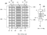
- FIG. 1 A known GaN based power amplifier is shown in figure 1 .
- a packaged power amplifier 100 is shown in which a gallium nitride die 30 is mounted on a heat conducting substrate 15.
- a field-effect transistor, FET is integrated, such as a high-electron mobility transistor, HEMT.
- Packaged power amplifier 100 further comprises a pair of RF input leads 10A, 10B, and a pair of RF output leads 20A, 20B.
- the packaged power amplifier comprises more leads for inputting and outputting control signals, DC power, etc. but these are omitted for illustrative purposes.
- packaged power amplifier 100 is a leadframe based package. It may comprise a cover (not shown) in the form of a cover or lid. Alternatively, the lid or cover is formed using a solidified molding compound which may or may not cover dies 30, 40, 50.
- packaged power amplifier 100 also comprises an input semiconductor die 40 and an output semiconductor die 50. On these dies, one or more capacitors are integrated. Dies 40, 50 may for example be silicon or gallium arsenide based. Alternatively, non-semiconductor materials may be used.
- the FET on GaN die 30 comprises a plurality of FET cells U1, U4, U5, U8 that are adjacently arranged in a row.
- An example of a FET cell 200 is illustrated in more detail on the right in figure 1 . Together, these FET cells form a single FET.
- Each FET cell 200 comprises a gate base Bg, one or more gate bond pads that are integrally formed or connected to gate base Bg, and one or more gate fingers g1, g2 extending from gate base Bg.
- the combined gate width of the one or more gate fingers g1, g2 in a given FET cell is referred to as the total FET cell gate width Uw.
- two gate fingers g1, g2 are used, each having a gate width Wg.
- the total FET cell gate width therefore equals 2Wg.
- Each FET 200 cell further comprises a drain base Bd and one or more drain fingers d extending from drain base Bd.
- Each FET cell 200 also comprises one or more drain bond pads that are integrally formed or connected to drain base Bd, and one or more source contacts s1, s2. These latter contacts are typically grounded during operation.
- GaN die 130 may be provided with vias that provide an electrical connection between the one more source contacts s1, s2 and the backside of GaN die 130. This latter backside is typically covered with a metal and is physically and electrically connected to heat conducting substrate 15.
- heat conducting substrate 15 is made of electrically conductive material.
- Power amplifier 100 is typically mounted on a printed circuit board, PCB, wherein heat conducting substrate 15 is connected to a ground patch, metal coin, or other ground terminal on the PCB.
- a plurality of bondwires connects RF input leads 10A, 10B to the gate terminal of the FET. More in particular, second input bondwires 43 connect RF input leads 10A, 10B to a first terminal 41 of an input matching capacitor that is integrated on input semiconductor die 40, and first input bondwires 42 connect first terminal 41 of the input matching capacitor to the gate bond pads of the FET. The other terminal of the input matching capacitor is grounded.
- first output bondwires 52 connect the drain bond pads of the FET to a first terminal 51 of an output matching capacitor that is integrated on output semiconductor die 50
- second output bondwires 53 connect first terminal 51 of the output matching capacitor to RF output leads 20A, 20B.
- the other terminal of the output matching capacitor is grounded.
- Bondwires 42, 43 and the input matching capacitor jointly form an input impedance matching network.
- bondwires 52, 53 and the output matching capacitor jointly form an output impedance matching network.
- the input and/or output matching capacitor is omitted.
- each FET cell 200 a respective input capacitor and/or a respective output capacitor may be used. In this case, the non-grounded terminals of these capacitors may not be electrically connected to each other. In other embodiments, a single capacitor is used for the input and/or output capacitor. In this case, each FET cell is associated with a segment of said single capacitor, wherein the non-grounded terminals of the segments are integrally connected.
- the respective capacitor or the segment of a single capacitor associated with a FET cell will be referred to as capacitive element.
- this capacitive element may be part of a plurality of capacitive elements of which the non-grounded terminals are connected, as shown in figure 1 , or of which the non-grounded terminals are isolated from each other. Furthermore, a distinction will hereinafter be made between output capacitive elements formed on semiconductor die 50 or other substrate, and input capacitive elements formed on semiconductor die 40 or other substrate.
- figure 1 illustrates a single input impedance matching stage and a single output matching stage, multiples of these stages may be used.
- Input semiconductor die 40 and output semiconductor die 50 may each have a conducting substrate, or vias formed in an otherwise non-conducting substrate to allow the other terminal of the input or output capacitor to be electrically connected to heat conducting substrate 15, which is exposed on a backside of packaged power amplifier 100 and which also serves as a ground terminal of packaged power amplifier 100.
- the one or more drain bond pads are electrically connected to the first terminal of a respective output capacitive element among the plurality of output capacitive elements using one or more first output bondwires 52 among the plurality of first output bondwires 52.
- the one or more first output bondwires 52 at least partially form, for said FET cell, a first inductor between the drain base Bd of that FET cell and the first terminal 51 of the output capacitive element to which that FET cell is connected.
- the operating frequency of the packaged amplifier 100 limits the gate width per gate finger that can be used. To obtain amplifiers delivering more output power, it is therefore necessary to increase the number of FET cells.
- US2021167741A1 discloses an input matching circuit, at least one amplifying transistor that receives a signal from the input matching circuit, a first dummy transistor that receives a signal from the input matching circuit, a second dummy transistor that receives a signal from the input matching circuit, and an output matching circuit that outputs an output of the amplifying transistor.
- the amplifying transistor is arranged between the first dummy transistor and the second dummy transistor, the amplifying transistor, the first dummy transistor. Furthermore, the second dummy transistor is provided in a row along the input matching circuit.
- US6815740B2 discloses a FET or BJT structure or distributed transistor amplifier having a tapered gate feed line and a tapered channel width (tapered source fingers, tapered drain fingers) that provides increased bandwidth and gain in the microwave/mm-wave frequency spectrum.
- this object is achieved using the power amplifier as defined in claim 1 that is characterized in that for FET cells arranged at opposing ends of the row of FET cells a total FET cell gate width and an inductance of the first inductor is larger and smaller than the total FET cell gate width and inductance of the first inductor for one or more FET cells arranged in the middle of the row of FET cells, respectively.
- the Applicant has found that in prior art devices, power is not generated uniformly. More in particular, power is generated more in the center FET cells. To address this asymmetry while maintaining a same total gate width, gate width for the center FET cell(s) is reduced compared to outer FET cells. At the same time, to account for the change in output impedance as a result of changing the gate width of the FET cell(s), the inductance of the first inductor changes. More specifically, the inductance of the first inductor for the center FET cell(s) is higher than that of the first inductor for the outer FET cells.
- the plurality of FET cells can be an even number of FET cells.
- the row of FET cells extends from a first outer FET cell to a first center FET cell, and from a second center FET cell to a second outer FET cell, wherein the first and second center FET cells are adjacently arranged and wherein the first outer FET cell and the second outer FET cell are arranged at opposite ends of the row of FET cells.
- the total FET cell gate width and the inductance of the first inductor then decreases and increases, respectively, from the first outer FET cell to the first center FET cell, and increases and decreases, respectively, from the second center FET cell to the second outer FET cell.
- the plurality of FET cells can be an odd number of FET cells.
- the row of unit cells extends from a first outer FET cell to a center FET cell, and from the center FET cell to a second outer FET cell, wherein the first and second outer FET cells are arranged at opposite ends of the row of FET cells.
- the total FET cell gate width and the inductance of the first inductor decreases and increases, respectively from the first outer FET cell to the center FET cell and increases and decreases, respectively, from the center FET cell to the second outer FET cell.
- the increase and decrease of the inductance of the first inductor and the increase and decrease of the total FET cell gate width can be monotonic.
- each FET cell may see an output impedance at its intrinsic drain.
- the abovementioned increase or decrease in total FET cell gate width and the corresponding decrease or increase in inductance of the first inductor can be configured for minimizing a difference between the output impedances seen by the plurality of FET cells during these predefined operating conditions.
- the predefined operating conditions can be conditions at which the output power of the power amplifier is saturated at a frequency within an operational bandwidth of the power amplifier.
- the output impedance can be a large-signal impedance or a small-signal impedance.
- the number of gate fingers and/or the gate width of the gate finger(s) may differ among the FET cells.
- the first inductor for each FET cell can be formed using one or more first output bondwires among a plurality of first output bondwires, wherein for the purpose of decreasing or increasing the inductance of the first inductor the number of first output bondwires, the height of the first output bondwire(s), and/or the length of the first output bondwire(s) may differ among the FET cells.
- the FET cells may comprise a gate base and one or more gate fingers extending from the gate base, wherein the total FET cell gate width corresponds to the combined width of the one or more gate fingers.
- the FET cells may further comprise a drain base, one or more drain fingers extending from the drain base, and one or more drain bond pads that are integrally formed or connected to the drain base.
- the FET cells may also comprise one or more source contacts. In some embodiments, these latter contacts are grounded during operation by one or more vias in the GaN semiconductor die that connects the contacts to the backside of the GaN semiconductor die, which is typically covered by a backside metallization.
- the GaN semiconductor die can be mounted on a heat conducting substrate or other metal part that is grounded during use.
- the corresponding gate bases are preferably in physical and electrical contact and the corresponding drain bases are preferably in physical and electrical contact. In this manner, drain and gate bars are formed.
- the power amplifier may further comprise a plurality of output capacitive elements, each having a first terminal and a grounded second terminal, and a plurality of second output bondwires.
- the one or more drain bond pads can be electrically connected to the first terminal of a respective output capacitive element among the plurality of output capacitive elements using one or more first output bondwires among the plurality of first output bondwires, wherein the one or more first output bondwires at least partially form, for said FET cell, the first inductor that is arranged between the drain base of that FET cell and the first terminal of the output capacitive element to which that FET cell is connected.
- first terminals of the output capacitive elements can be connected directly or indirectly to the one or more RF output terminals using the plurality of second output bondwires.
- the first terminals of the output capacitive elements can be physically connected for forming a single terminal, wherein the output capacitive elements correspond to segments of a single capacitor.
- the capacitive elements are electrically isolated from each other.
- the one or more output capacitive elements, the plurality of first output bondwires, and the plurality of second output bondwires may jointly form output impedance matching stages between the drain bases of the FET cells and the one or more output RF terminals.
- the power amplifier may comprise an output substrate, such as a semiconductor die, on which the output capacitive elements are integrated.
- the power amplifier may comprise one or more RF input terminals.
- the FET cells can be connected to the one or more RF input terminals either directly or indirectly via a respective second inductor.
- an inductance of the second inductor can be smaller, respectively, than the inductance of the second inductor for one or more FET cells arranged in the middle of the row of FET cells.
- the second inductor for each FET cell can be formed using one or more first input bondwires among a plurality of first input bondwires, wherein for the purpose of decreasing or increasing the inductance of the second inductor the number of first input bondwires, the height of the first input bondwire(s), and/or the length of the first input bondwire(s) may differ among the FET cells.
- Each FET cell may comprise one or more gate bond pads integrally formed or connected to the gate base.
- the power amplifier may further comprise a plurality of input capacitive elements, each having a first terminal and a grounded second terminal, and a plurality of second input bondwires.
- the one or more gate bond pads can be electrically connected to the first terminal of a respective input capacitive element among the plurality of input capacitive elements using one or more first input bondwires among the plurality of first input bondwires.
- the one or more first input bondwires may at least partially form, for the FET cell, the second inductor that is arranged between the gate base of that FET cell and the first terminal of the input capacitive element to which that FET cell is connected.
- the first terminals of the input capacitive elements can be connected directly or indirectly to the one or more RF input terminals using the plurality of second input bondwires.
- the first terminals of the input capacitive elements can be physically connected for forming a single terminal, wherein the input capacitive elements may correspond to segments of a single capacitor.
- the plurality of input capacitive elements, the plurality of first input bondwires, and the plurality of second input bondwires may jointly form one or more input impedance matching stages between the one or more RF input terminals and the gates bases of the FET cells.
- the power amplifier may comprise an input substrate, such as a semiconductor die, on which the input capacitive elements can be integrated.
- a ratio between the total gate width of a FET cell arranged in or near the middle of the row of FET cells and the total gate width of a FET cell arranged at an end of the row of FET cells may lie in between 0.5 and 0.9, and/or a ratio between the inductance of the first inductor of a FET cell arranged in or near the middle of the row of FET cells and the inductance of the first inductor of a FET cell arranged at an end of the row of FET cells may lie in between 1.1 and 2.
- the power amplifier can be a packaged power amplifier, comprising a heat conducting substrate on which the GaN die and the input and output substrate, when applicable, are arranged.
- the heat conducting substrate may comprise a copper block or copper based block.
- the packaged power amplifier can be in the form of a flat no-leads package, such as a dual flat no-leads package, DFN, or quad flat no-leads package, QFN.
- the packaged power amplifier may comprise a leadframe package having a plurality of leads forming the one or more RF input terminals and/or the one or more RF output terminals.
- the present invention provides a Doherty amplifier comprising a main amplifier and one or more peak amplifiers, wherein at least one of the main amplifier and the one or more peak amplifiers comprises the power amplifier as described above.
- the main amplifier and the one or more peak amplifiers are packaged power amplifiers, the main amplifier and at least one among the one or more peak amplifiers can be arranged inside a same package.
- FIG 2 illustrates an equivalent circuit of a segment of the power amplifier of figure 1 .
- FET Qn is a representation of the n th FET cell of which the layout is depicted on the right hand side in figure 1 .
- inductor L1,n represents bondwires 43, and inductor L2,n bondwires 42 that are connected to this FET cell.
- capacitor C1,n represents a segment of the capacitor realized on semiconductor die 40 that is associated with this FET cell.
- This n th FET cell has an output capacitance that is modelled by C2,n.
- Z,n-1 represents the impedance seen at the drain of the n th FET cell looking towards the (n-1) th cell and Z,n+1 represents the impedance seen at the drain of the n th FET cell looking towards the (n+1) th cell.
- L3,n represents bondwires 52, and inductor L4,n bondwires 53 that are connected to this FET cell.
- capacitor C3,n represents a segment of the capacitor realized on semiconductor die 50 that is associated with this FET cell.
- L1,n, C1,n, and L2,n jointly form an input impedance matching network
- L3,n, C3,n, and L4,n jointly form an output impedance matching network.
- L3,n is referred to as the first inductor
- L2,n as the second inductor.
- the RF input of the n th FET cell referred to as RFin,n in figure 2
- the RF output of the n th FET cell referred to as RFout,n in figure 2
- the RF output of the n th FET cell is connected to other RF outputs on one of the RF output terminals 20A, 20B.
- this imbalance is addressed by using cells at the ends of the row that have a larger total FET cell gate width and a smaller inductance of inductor L3,n than FET cells that are arranged in the middle of the row of FET cells.
- An example of such a power amplifier is shown in figure 3 .
- Amplifier 1 comprises the same components as amplifier 100, and the various components of amplifier 1 are therefore denoted using the same reference signs.
- Amplifier 1 differs from amplifier 100 shown in figure 1 in that FET cells U1, U8 have an increased total FET cell gate width compared to the other FET cells that is exemplified by the wider gate fingers.
- FET cells U1, U8 have a reduced inductance that is associated with inductor L3,n compared to the other FET cells. This reduction has been achieved by including an extra bondwire compared to FET cells U2, U3, U4, U5, U6, and U7.
- FET cells U4, U5 have a reduced total FET cell gate width compared to the other FET cells that is exemplified by those cells lacking one gate finger compared to the other FET cells.
- FET cells U4, U5 have an increased inductance that is associated with inductor L3,n compared to the other FET cells. This reduction has been achieved by omitting one of two bondwires when compared to FET cells U2, U3, U6, and U7.
- the inductance associated with L3,n preferably increases monotonically going from an end of the row of FET cells to a center of the row of FET cells.
- the total gate width of a FET cell preferably decreases monotonically going from an end of the row of FET cells to a center of the row of FET cells.
- Uw,n a number of FET cells
- Uw,n e.g.
- the inductance associated with L3,n is identical for all FET cells except for FET cells U4, U5.
- a more gradual increase in inductance is used.
- the number of bondwires, the bondwire shape, length, and/or height are varied between adjacent FET cells.
- the inductance value associated with L3,n is preferably changed in accordance with the change in total FET cell gate width. More specifically, for increased total FET cell gate widths, a reduced inductance is preferably used. In some embodiments, similar modifications can be used for inductance L2,n. In even further embodiments, not only L3,n, but also C3,n, and/or L4,n can be adapted to accommodate for the different total FET cell gate width. In general, the adaptations should be such that a difference in the output impedances seen by the different FET cells is lowered. The same approach could be followed for L1,n, but also C1,n, and/or L2,n. In this case, the adaptations should be such that a difference in the input impedances of the different FET cells is lowered.
- capacitors C3,n and C1,n are electrically connected as these terminals correspond to segments of a larger conductive terminal of the capacitor formed on semiconductor dies 40, 50.
- the non-grounded terminals may be disconnected from each other, leaving only a common ground connected of the grounded terminals. In such case, capacitors C3,n and C1,n act as separate capacitors.
- a GaN based amplifier having a total gate width of 25.2 mm having a standard design was compared to a GaN based amplifier having a design in accordance with the present invention in which the same total gate width was used but in which the total gate width for the center FET cells was reduced whereas it was increased for the outer FET cells.
- this latter design one bondwire was omitted for the center FET cells only. This comparison demonstrated that for the new design, the saturated power was increased from 52.9 dBm to 53.5 dBm, and the maximum power added efficiency was increased from 65.1 to 72 percent.
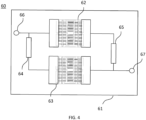
- FIG 4 illustrates an embodiment of a Doherty amplifier 60 in accordance with the present invention.
- Doherty amplifier 60 comprises a main amplifier 62 and a peak amplifier 63 that are both mounted on a printed circuit board 61. More in particular, main amplifier 62 and peak amplifier 63 each comprise a packaged power amplifier similar to packaged power amplifier 1 shown in figure 3 .
- Doherty amplifier 60 has an RF input 66 and an RF output 67.
- An RF signal entering RF input 66 will be split in two parts, one part for main amplifier 62 and one part for peak amplifier 63. This latter part is delayed by 90 degrees at the operational frequency by phase delay unit 64.
- the signals amplified by main amplifier 62 and peak amplifier 63 are outputted at RF output 67.
- the signal outputted by main amplifier 62 is fed through an impedance inverter 65, which is typically formed using a 90 degrees transmission line or an electrical equivalent thereof. In this manner, a desired load modulation of the impedance seen by main amplifier 62 is obtained whereas at the same time, signals are added in-phase at RF output 67.
- the Doherty configuration shown in figure 4 is known as a regular Doherty configuration. However, different Doherty configurations are known, such as a parallel Doherty configuration, and an inverted Doherty configuration. The present invention is equally applicably to those configurations.
- figure 4 shown an amplifier having two discrete packages.
- the main and peak amplifier are packaged in a same leadframe based package or other package.
- figure 4 shows a single main amplifier and a single peak amplifier.
- the present invention is equally applicable to multi-stage Doherty amplifiers in which two or more peak amplifiers are used.
Landscapes
- Engineering & Computer Science (AREA)
- Power Engineering (AREA)
- Microelectronics & Electronic Packaging (AREA)
- Amplifiers (AREA)
Description
- The present invention relates to a power amplifier and to a Doherty amplifier comprising the same. The present invention particularly relates to gallium nitride, GaN, power amplifiers operating at radiofrequency, RF, frequencies between 0.5 and 6 GHz, and at relatively high powers, e.g. in excess of 200 Watt.
- A known GaN based power amplifier is shown in
figure 1 . Infigure 1 , a packagedpower amplifier 100 is shown in which a gallium nitride die 30 is mounted on aheat conducting substrate 15. On semiconductor die 30, a field-effect transistor, FET, is integrated, such as a high-electron mobility transistor, HEMT. - Packaged
power amplifier 100 further comprises a pair of RF input leads 10A, 10B, and a pair of RF output leads 20A, 20B. Generally, the packaged power amplifier comprises more leads for inputting and outputting control signals, DC power, etc. but these are omitted for illustrative purposes. Furthermore, packagedpower amplifier 100 is a leadframe based package. It may comprise a cover (not shown) in the form of a cover or lid. Alternatively, the lid or cover is formed using a solidified molding compound which may or may not cover dies 30, 40, 50. - In addition to semiconductor die 30, packaged
power amplifier 100 also comprises an input semiconductor die 40 and an output semiconductor die 50. On these dies, one or more capacitors are integrated.Dies - The FET on GaN die 30 comprises a plurality of FET cells U1, U4, U5, U8 that are adjacently arranged in a row. An example of a
FET cell 200 is illustrated in more detail on the right infigure 1 . Together, these FET cells form a single FET. - Each
FET cell 200 comprises a gate base Bg, one or more gate bond pads that are integrally formed or connected to gate base Bg, and one or more gate fingers g1, g2 extending from gate base Bg. The combined gate width of the one or more gate fingers g1, g2 in a given FET cell is referred to as the total FET cell gate width Uw. Infigure 1 , two gate fingers g1, g2 are used, each having a gate width Wg. The total FET cell gate width therefore equals 2Wg. - Each
FET 200 cell further comprises a drain base Bd and one or more drain fingers d extending from drain base Bd. EachFET cell 200 also comprises one or more drain bond pads that are integrally formed or connected to drain base Bd, and one or more source contacts s1, s2. These latter contacts are typically grounded during operation. For example, GaN die 130 may be provided with vias that provide an electrical connection between the one more source contacts s1, s2 and the backside of GaN die 130. This latter backside is typically covered with a metal and is physically and electrically connected toheat conducting substrate 15. Furthermore,heat conducting substrate 15 is made of electrically conductive material.Power amplifier 100 is typically mounted on a printed circuit board, PCB, whereinheat conducting substrate 15 is connected to a ground patch, metal coin, or other ground terminal on the PCB. - A plurality of bondwires connects RF input leads 10A, 10B to the gate terminal of the FET. More in particular,
second input bondwires 43 connect RF input leads 10A, 10B to afirst terminal 41 of an input matching capacitor that is integrated oninput semiconductor die 40, andfirst input bondwires 42 connectfirst terminal 41 of the input matching capacitor to the gate bond pads of the FET. The other terminal of the input matching capacitor is grounded. - Similarly, a plurality of output bondwires connects RF output leads 20A, 20B to the drain terminal of the FET. More in particular,
first output bondwires 52 connect the drain bond pads of the FET to afirst terminal 51 of an output matching capacitor that is integrated onoutput semiconductor die 50, andsecond output bondwires 53 connectfirst terminal 51 of the output matching capacitor to RF output leads 20A, 20B. The other terminal of the output matching capacitor is grounded. - Bondwires 42, 43 and the input matching capacitor jointly form an input impedance matching network. Similarly,
bondwires - For each
FET cell 200, a respective input capacitor and/or a respective output capacitor may be used. In this case, the non-grounded terminals of these capacitors may not be electrically connected to each other. In other embodiments, a single capacitor is used for the input and/or output capacitor. In this case, each FET cell is associated with a segment of said single capacitor, wherein the non-grounded terminals of the segments are integrally connected. Hereinafter, the respective capacitor or the segment of a single capacitor associated with a FET cell will be referred to as capacitive element. As described above, this capacitive element may be part of a plurality of capacitive elements of which the non-grounded terminals are connected, as shown infigure 1 , or of which the non-grounded terminals are isolated from each other. Furthermore, a distinction will hereinafter be made between output capacitive elements formed on semiconductor die 50 or other substrate, and input capacitive elements formed on semiconductor die 40 or other substrate. - Although
figure 1 illustrates a single input impedance matching stage and a single output matching stage, multiples of these stages may be used. - Input semiconductor die 40 and output semiconductor die 50 may each have a conducting substrate, or vias formed in an otherwise non-conducting substrate to allow the other terminal of the input or output capacitor to be electrically connected to
heat conducting substrate 15, which is exposed on a backside of packagedpower amplifier 100 and which also serves as a ground terminal of packagedpower amplifier 100. - For each
FET cell 200, the one or more drain bond pads are electrically connected to the first terminal of a respective output capacitive element among the plurality of output capacitive elements using one or morefirst output bondwires 52 among the plurality offirst output bondwires 52. The one or morefirst output bondwires 52 at least partially form, for said FET cell, a first inductor between the drain base Bd of that FET cell and thefirst terminal 51 of the output capacitive element to which that FET cell is connected. - Typically, the operating frequency of the packaged
amplifier 100 limits the gate width per gate finger that can be used. To obtain amplifiers delivering more output power, it is therefore necessary to increase the number of FET cells. -
US2021167741A1 discloses an input matching circuit, at least one amplifying transistor that receives a signal from the input matching circuit, a first dummy transistor that receives a signal from the input matching circuit, a second dummy transistor that receives a signal from the input matching circuit, and an output matching circuit that outputs an output of the amplifying transistor. The amplifying transistor is arranged between the first dummy transistor and the second dummy transistor, the amplifying transistor, the first dummy transistor. Furthermore, the second dummy transistor is provided in a row along the input matching circuit. -
US6815740B2 discloses a FET or BJT structure or distributed transistor amplifier having a tapered gate feed line and a tapered channel width (tapered source fingers, tapered drain fingers) that provides increased bandwidth and gain in the microwave/mm-wave frequency spectrum. - The Applicant has found that in particular with GaN FETs, increasing the number of FET cells often will not result in the expected power scaling. For example, selecting twice the number of FET cells will not double output power. Instead, the obtained output power is less than doubled although the power consumption of the FET is doubled. Consequently, power efficiency of the FET will drop for larger FET devices.
- It is an object of the present invention to provide a power amplifier in which the abovementioned scaling problem is addressed and which displays improved power added efficiency.
- According to the present invention, this object is achieved using the power amplifier as defined in
claim 1 that is characterized in that for FET cells arranged at opposing ends of the row of FET cells a total FET cell gate width and an inductance of the first inductor is larger and smaller than the total FET cell gate width and inductance of the first inductor for one or more FET cells arranged in the middle of the row of FET cells, respectively. - The Applicant has found that in prior art devices, power is not generated uniformly. More in particular, power is generated more in the center FET cells. To address this asymmetry while maintaining a same total gate width, gate width for the center FET cell(s) is reduced compared to outer FET cells. At the same time, to account for the change in output impedance as a result of changing the gate width of the FET cell(s), the inductance of the first inductor changes. More specifically, the inductance of the first inductor for the center FET cell(s) is higher than that of the first inductor for the outer FET cells.
- The plurality of FET cells can be an even number of FET cells. In this case, the row of FET cells extends from a first outer FET cell to a first center FET cell, and from a second center FET cell to a second outer FET cell, wherein the first and second center FET cells are adjacently arranged and wherein the first outer FET cell and the second outer FET cell are arranged at opposite ends of the row of FET cells. The total FET cell gate width and the inductance of the first inductor then decreases and increases, respectively, from the first outer FET cell to the first center FET cell, and increases and decreases, respectively, from the second center FET cell to the second outer FET cell.
- Alternatively, the plurality of FET cells can be an odd number of FET cells. In this case, the row of unit cells extends from a first outer FET cell to a center FET cell, and from the center FET cell to a second outer FET cell, wherein the first and second outer FET cells are arranged at opposite ends of the row of FET cells. The total FET cell gate width and the inductance of the first inductor decreases and increases, respectively from the first outer FET cell to the center FET cell and increases and decreases, respectively, from the center FET cell to the second outer FET cell.
- In both odd and even configurations, the increase and decrease of the inductance of the first inductor and the increase and decrease of the total FET cell gate width can be monotonic.
- During predefined operating conditions, each FET cell may see an output impedance at its intrinsic drain. The abovementioned increase or decrease in total FET cell gate width and the corresponding decrease or increase in inductance of the first inductor can be configured for minimizing a difference between the output impedances seen by the plurality of FET cells during these predefined operating conditions. For example, the predefined operating conditions can be conditions at which the output power of the power amplifier is saturated at a frequency within an operational bandwidth of the power amplifier. Furthermore, the output impedance can be a large-signal impedance or a small-signal impedance.
- For the purpose of decreasing or increasing the total FET cell gate width, the number of gate fingers and/or the gate width of the gate finger(s) may differ among the FET cells.
- Additionally or alternatively, the first inductor for each FET cell can be formed using one or more first output bondwires among a plurality of first output bondwires, wherein for the purpose of decreasing or increasing the inductance of the first inductor the number of first output bondwires, the height of the first output bondwire(s), and/or the length of the first output bondwire(s) may differ among the FET cells.
- The FET cells may comprise a gate base and one or more gate fingers extending from the gate base, wherein the total FET cell gate width corresponds to the combined width of the one or more gate fingers. The FET cells may further comprise a drain base, one or more drain fingers extending from the drain base, and one or more drain bond pads that are integrally formed or connected to the drain base. The FET cells may also comprise one or more source contacts. In some embodiments, these latter contacts are grounded during operation by one or more vias in the GaN semiconductor die that connects the contacts to the backside of the GaN semiconductor die, which is typically covered by a backside metallization. In turn, the GaN semiconductor die can be mounted on a heat conducting substrate or other metal part that is grounded during use.
- For each pair of adjacently arranged FET cells, the corresponding gate bases are preferably in physical and electrical contact and the corresponding drain bases are preferably in physical and electrical contact. In this manner, drain and gate bars are formed.
- The power amplifier may further comprise a plurality of output capacitive elements, each having a first terminal and a grounded second terminal, and a plurality of second output bondwires. For each FET cell, the one or more drain bond pads can be electrically connected to the first terminal of a respective output capacitive element among the plurality of output capacitive elements using one or more first output bondwires among the plurality of first output bondwires, wherein the one or more first output bondwires at least partially form, for said FET cell, the first inductor that is arranged between the drain base of that FET cell and the first terminal of the output capacitive element to which that FET cell is connected. Moreover, the first terminals of the output capacitive elements can be connected directly or indirectly to the one or more RF output terminals using the plurality of second output bondwires. The first terminals of the output capacitive elements can be physically connected for forming a single terminal, wherein the output capacitive elements correspond to segments of a single capacitor. Alternatively, the capacitive elements are electrically isolated from each other.
- The one or more output capacitive elements, the plurality of first output bondwires, and the plurality of second output bondwires may jointly form output impedance matching stages between the drain bases of the FET cells and the one or more output RF terminals.
- For realizing the output capacitive elements, the power amplifier may comprise an output substrate, such as a semiconductor die, on which the output capacitive elements are integrated.
- The power amplifier may comprise one or more RF input terminals. Furthermore, the FET cells can be connected to the one or more RF input terminals either directly or indirectly via a respective second inductor. For FET cells arranged at opposing ends of the row of FET cells, an inductance of the second inductor can be smaller, respectively, than the inductance of the second inductor for one or more FET cells arranged in the middle of the row of FET cells. For example, the second inductor for each FET cell can be formed using one or more first input bondwires among a plurality of first input bondwires, wherein for the purpose of decreasing or increasing the inductance of the second inductor the number of first input bondwires, the height of the first input bondwire(s), and/or the length of the first input bondwire(s) may differ among the FET cells.
- Each FET cell may comprise one or more gate bond pads integrally formed or connected to the gate base. In addition, the power amplifier may further comprise a plurality of input capacitive elements, each having a first terminal and a grounded second terminal, and a plurality of second input bondwires. For each FET cell, the one or more gate bond pads can be electrically connected to the first terminal of a respective input capacitive element among the plurality of input capacitive elements using one or more first input bondwires among the plurality of first input bondwires. The one or more first input bondwires may at least partially form, for the FET cell, the second inductor that is arranged between the gate base of that FET cell and the first terminal of the input capacitive element to which that FET cell is connected. Moreover, the first terminals of the input capacitive elements can be connected directly or indirectly to the one or more RF input terminals using the plurality of second input bondwires.
- Similarly to the output capacitive elements, the first terminals of the input capacitive elements can be physically connected for forming a single terminal, wherein the input capacitive elements may correspond to segments of a single capacitor.
- The plurality of input capacitive elements, the plurality of first input bondwires, and the plurality of second input bondwires may jointly form one or more input impedance matching stages between the one or more RF input terminals and the gates bases of the FET cells.
- The power amplifier may comprise an input substrate, such as a semiconductor die, on which the input capacitive elements can be integrated.
- A ratio between the total gate width of a FET cell arranged in or near the middle of the row of FET cells and the total gate width of a FET cell arranged at an end of the row of FET cells may lie in between 0.5 and 0.9, and/or a ratio between the inductance of the first inductor of a FET cell arranged in or near the middle of the row of FET cells and the inductance of the first inductor of a FET cell arranged at an end of the row of FET cells may lie in between 1.1 and 2.
- The power amplifier can be a packaged power amplifier, comprising a heat conducting substrate on which the GaN die and the input and output substrate, when applicable, are arranged. The heat conducting substrate may comprise a copper block or copper based block. The packaged power amplifier can be in the form of a flat no-leads package, such as a dual flat no-leads package, DFN, or quad flat no-leads package, QFN. Alternatively, the packaged power amplifier may comprise a leadframe package having a plurality of leads forming the one or more RF input terminals and/or the one or more RF output terminals.
- According to a second aspect, the present invention provides a Doherty amplifier comprising a main amplifier and one or more peak amplifiers, wherein at least one of the main amplifier and the one or more peak amplifiers comprises the power amplifier as described above. When the main amplifier and the one or more peak amplifiers are packaged power amplifiers, the main amplifier and at least one among the one or more peak amplifiers can be arranged inside a same package.
- Next, the present invention will be described in more detail referring to the appended drawings, wherein:
-
Figure 1 illustrates a schematic layout of a known GaN based power amplifier; -
Figure 2 illustrates an equivalent circuit of a segment of the power amplifier offigure 1 ; -
Figure 3 illustrates an embodiment of a power amplifier according to the present invention; and -
Figure 4 illustrates an embodiment of a Doherty amplifier in accordance with the present invention. -
Figure 2 illustrates an equivalent circuit of a segment of the power amplifier offigure 1 . In this figure, FET Qn is a representation of the nth FET cell of which the layout is depicted on the right hand side infigure 1 . Furthermore, inductor L1,n representsbondwires 43, and inductor L2,n bondwires 42 that are connected to this FET cell. Similarly, capacitor C1,n represents a segment of the capacitor realized on semiconductor die 40 that is associated with this FET cell. This nth FET cell has an output capacitance that is modelled by C2,n. Z,n-1 represents the impedance seen at the drain of the nth FET cell looking towards the (n-1)th cell and Z,n+1 represents the impedance seen at the drain of the nth FET cell looking towards the (n+1)th cell. L3,n representsbondwires 52, and inductor L4,n bondwires 53 that are connected to this FET cell. In addition, capacitor C3,n represents a segment of the capacitor realized on semiconductor die 50 that is associated with this FET cell. - L1,n, C1,n, and L2,n jointly form an input impedance matching network, and L3,n, C3,n, and L4,n jointly form an output impedance matching network. Furthermore, L3,n is referred to as the first inductor, and L2,n as the second inductor.
- The RF input of the nth FET cell, referred to as RFin,n in
figure 2 , is connected to other RF inputs on one of theRF input terminals figure 2 , is connected to other RF outputs on one of theRF output terminals - The Applicant had found that an important source of the unequal power distribution in the FET can be attributed to the different effects impedances Z,n-1 and Z,n+1 have on the impedance seen by the various FET cells. More in particular, at the ends of the row of FET cells, such impedance is only present in one direction. Put differently, in
figure 1 , Z,0 and Z,9 are infinite. Consequently, the impedance seen by FET cells in the center of the row is lower than that at the ends of the row. - According to the present invention, this imbalance is addressed by using cells at the ends of the row that have a larger total FET cell gate width and a smaller inductance of inductor L3,n than FET cells that are arranged in the middle of the row of FET cells. An example of such a power amplifier is shown in
figure 3 . - In
figure 3 , an embodiment of apower amplifier 1 in accordance with the present invention is shown.Amplifier 1 comprises the same components asamplifier 100, and the various components ofamplifier 1 are therefore denoted using the same reference signs. -
Amplifier 1 differs fromamplifier 100 shown infigure 1 in that FET cells U1, U8 have an increased total FET cell gate width compared to the other FET cells that is exemplified by the wider gate fingers. In addition, FET cells U1, U8 have a reduced inductance that is associated with inductor L3,n compared to the other FET cells. This reduction has been achieved by including an extra bondwire compared to FET cells U2, U3, U4, U5, U6, and U7. - On the other hand, FET cells U4, U5 have a reduced total FET cell gate width compared to the other FET cells that is exemplified by those cells lacking one gate finger compared to the other FET cells. In addition, FET cells U4, U5 have an increased inductance that is associated with inductor L3,n compared to the other FET cells. This reduction has been achieved by omitting one of two bondwires when compared to FET cells U2, U3, U6, and U7.
- The inductance associated with L3,n preferably increases monotonically going from an end of the row of FET cells to a center of the row of FET cells. For a power amplifier having an even number of FET cells, e.g. N cells, this means that L3,n >= L3,n-1 for 2 <= n <= N/2 and L3,n >= L3,n+1 for (N-1) >= n >= (N/2+1). For a power amplifier having an odd number of FET cells, e.g. M cells, this means that L3,n >= L3,n-1 for 2 <= n <= (M/2 +0.5) and L3,n >= L3,n+1 for (M-1) >= n >= (M/2+0.5).
- Similarly, the total gate width of a FET cell, denoted by Uw,n, preferably decreases monotonically going from an end of the row of FET cells to a center of the row of FET cells. For a power amplifier having an even number of FET cells, e.g. N cells, this means that Uw,n <= Uw,n-1 for 2 <= n <= N/2 and Uw,n <= Uw,n+1 for (N-1) >= n > (N/2+1). For a power amplifier having an even number of FET cells, e.g. M cells, this means that Uw,n <= Uw,n-1 for 2 <= n <= (M/2+0.5) and Uw,n <= Uw,n+1 for (M-1) >= n >= (M/2+0.5).
- As show in
figure 3 , the inductance associated with L3,n is identical for all FET cells except for FET cells U4, U5. In some embodiments, for increasing manufacturability, it is preferred to use the same bondwire shape and length forbondwires 52 as much as possible. In those cases, inductance can only be changed by changing the number of bondwires. - In other embodiments, a more gradual increase in inductance is used. In these embodiments, the number of bondwires, the bondwire shape, length, and/or height are varied between adjacent FET cells.
- Similar considerations hold for changing the total FET gate width. In
figure 3 , the total FET cell gate width has been increased by changing the gate width of a single finger, whereas a reduction in total FET cell gate width has achieved by omitting a gate finger relative to the other FET cells. Various combinations are possible within the scope of the present invention. More in particular, a change in total FET cell gate width can be obtained by changing the number and/or width of the gate fingers of a FET cell. - Notwithstanding the abovementioned aspect of manufacturability, the inductance value associated with L3,n is preferably changed in accordance with the change in total FET cell gate width. More specifically, for increased total FET cell gate widths, a reduced inductance is preferably used. In some embodiments, similar modifications can be used for inductance L2,n. In even further embodiments, not only L3,n, but also C3,n, and/or L4,n can be adapted to accommodate for the different total FET cell gate width. In general, the adaptations should be such that a difference in the output impedances seen by the different FET cells is lowered. The same approach could be followed for L1,n, but also C1,n, and/or L2,n. In this case, the adaptations should be such that a difference in the input impedances of the different FET cells is lowered.
- In addition, in
figure 3 a single capacitor is used both at the input and output. More in particular, the non-grounded terminals of capacitors C3,n and C1,n are electrically connected as these terminals correspond to segments of a larger conductive terminal of the capacitor formed on semiconductor dies 40, 50. In other embodiments, the non-grounded terminals may be disconnected from each other, leaving only a common ground connected of the grounded terminals. In such case, capacitors C3,n and C1,n act as separate capacitors. - A GaN based amplifier having a total gate width of 25.2 mm having a standard design was compared to a GaN based amplifier having a design in accordance with the present invention in which the same total gate width was used but in which the total gate width for the center FET cells was reduced whereas it was increased for the outer FET cells. In addition, in this latter design, one bondwire was omitted for the center FET cells only. This comparison demonstrated that for the new design, the saturated power was increased from 52.9 dBm to 53.5 dBm, and the maximum power added efficiency was increased from 65.1 to 72 percent.
-
Figure 4 illustrates an embodiment of aDoherty amplifier 60 in accordance with the present invention.Doherty amplifier 60 comprises amain amplifier 62 and apeak amplifier 63 that are both mounted on a printedcircuit board 61. More in particular,main amplifier 62 andpeak amplifier 63 each comprise a packaged power amplifier similar to packagedpower amplifier 1 shown infigure 3 . -
Doherty amplifier 60 has anRF input 66 and anRF output 67. An RF signal enteringRF input 66 will be split in two parts, one part formain amplifier 62 and one part forpeak amplifier 63. This latter part is delayed by 90 degrees at the operational frequency byphase delay unit 64. - The signals amplified by
main amplifier 62 andpeak amplifier 63 are outputted atRF output 67. However, the signal outputted bymain amplifier 62 is fed through animpedance inverter 65, which is typically formed using a 90 degrees transmission line or an electrical equivalent thereof. In this manner, a desired load modulation of the impedance seen bymain amplifier 62 is obtained whereas at the same time, signals are added in-phase atRF output 67. - The Doherty configuration shown in
figure 4 is known as a regular Doherty configuration. However, different Doherty configurations are known, such as a parallel Doherty configuration, and an inverted Doherty configuration. The present invention is equally applicably to those configurations. - In addition,
figure 4 shown an amplifier having two discrete packages. However, embodiments are equally possible in which the main and peak amplifier are packaged in a same leadframe based package or other package. - Finally,
figure 4 shows a single main amplifier and a single peak amplifier. However, the present invention is equally applicable to multi-stage Doherty amplifiers in which two or more peak amplifiers are used. - In the above, the present invention has been explained using detailed embodiments thereof. However, the present invention is not limited to these embodiments. Rather, various modifications are possible without deviating from the scope of the present invention, which is defined by the appended claims.
Claims (15)
- A power amplifier (1), comprising:one or more radiofrequency, RF, output terminals (20A, 20B); anda Gallium Nitride, GaN, semiconductor die (30) on which a power field-effect transistor, FET, is integrated, said FET comprising a plurality of FET cells (U1, U4, U5, U8) that are adjacently arranged in a row, wherein the FET cells (U1, U4, U5, U8) are connected either directly or indirectly to the one or more RF output terminals (20A, 20B) via a respective first inductor (L3,n),wherein, for FET cells (U1, U8) arranged at opposing ends of the row of FET cells:a total FET cell gate width (Uw) is larger than the total FET cell gate width (Uw) for one or more FET cells (U4, U5) arranged in the middle of the row of FET cells; andan inductance of the first inductor (L3,n) is smaller than the inductance of the first inductor (L3,n) for one or more FET cells (U4, U5) arranged in the middle of the row of FET cells.
- The power amplifier (1) according to claim 1, wherein said plurality of FET cells (U1, U4, U5, U8) is an even number of FET cells (U1, U4, U5, U8), and wherein the row of FET cells (U1, U4, U5, U8) extends from a first outer FET cell (U1) to a first center FET cell (U4), and from a second center FET cell (U5) to a second outer FET cell (U8), wherein the first and second center FET cells (U4, U5) are adjacently arranged and wherein the first outer FET cell (U1) and the second outer FET cell (U8) are arranged at opposite ends of the row of FET cells (U1, U4, U5, U8);wherein the total FET cell gate width (Uw) and the inductance of the first inductor (L3,n) decreases and increases, respectively, from the first outer FET cell (U1) to the first center FET cell (U4) and increases and decreases, respectively, from the second center FET cell (U5) to the second outer FET cell (U8);wherein said increase and decrease of the inductance of the first inductor (L3,n) and said increase and decrease of the total FET cell gate width (Uw) are preferably monotonic.
- The power amplifier (1) according to claim 1, wherein said plurality of FET cells is an odd number of FET cells, and wherein the row of unit cells extends from a first outer FET cell to a center FET cell, and from the center FET cell to a second outer FET cell, wherein the first and second outer FET cells are arranged at opposite ends of the row of FET cells;wherein the total FET cell gate width and the inductance of the first inductor (L3,n) decreases and increases, respectively from the first outer FET cell to the center FET cell and increases and decreases, respectively, from the center FET cell to the second outer FET cell;wherein said increase and decrease of the inductance of the first inductor (L3,n) and said increase and decrease of the total FET cell gate width (Uw) are preferably monotonic.
- The power amplifier (1) according to any of the previous claims, wherein during predefined operating conditions, each FET cell (U1, U4, U5, U8) sees an output impedance at its intrinsic drain, wherein said increase or decrease in total FET cell gate width (Uw) and said corresponding decrease or increase in inductance of the first inductor (L3,n) are configured for minimizing a difference between the output impedances seen by the plurality of FET cells (U1, U4, U5, U8) during said predefined operating conditions;
wherein the predefined operating conditions are preferably conditions at which the output power of the power amplifier (1) is saturated at a frequency within an operational bandwidth of the power amplifier (1), and/or wherein the output impedance is preferably a large-signal impedance or a small-signal impedance. - The power amplifier (1) according to any of the previous claims, wherein for the purpose of decreasing or increasing the total FET cell gate width the number of gate fingers and/or the gate width of the gate finger(s) differs among the FET cells (U1, U4, U5, U8).
- The power amplifier (1) according to any of the previous claims, wherein the first inductor (L3,n) for each FET cell (U1, U4, U5, U8) is formed using one or more first output bondwires (52) among a plurality of first output bondwires (52), wherein for the purpose of decreasing or increasing the inductance of the first inductor (L3,n):
the number of first output bondwires (52), the height of the first output bondwire(s) (52), and/or the length of the first output bondwire(s) (52) differs among the FET cells (U1, U4, U5, U8). - The power amplifier (1) according to any of the previous claims, wherein the FET cells comprise:a gate base (Bg) and one or more gate fingers (g1, g2) extending from the gate base (Bg), wherein the total FET cell gate width (Uw) corresponds to the combined width of the one or more gate fingers (g1, h2);a drain base (Bd) and one or more drain fingers (d) extending from the drain base (Bd);one or more drain bond pads integrally formed or connected to the drain base (Bd); andone or more source contacts (s1, s2);wherein for each pair of adjacently arranged FET cells (U1, U4, U5, U8), the corresponding gate bases (Bg) are preferably in physical and electrical contact and the corresponding drain bases (Bd) are in physical and electrical contact.
- The power amplifier (1) according to claim 7 and claim 6, further comprising:a plurality of output capacitive elements (C3, n), each having a first terminal (51) and a grounded second terminal; anda plurality of second output bondwires (53);wherein for each FET cell (U1, U4, U5, U8) the one or more drain bond pads are electrically connected to the first terminal (51) of a respective output capacitive element (C3,n) among the plurality of output capacitive elements (C3,n) using one or more first output bondwires (52) among the plurality of first output bondwires (52), said one or more first output bondwires (52) at least partially forming, for said FET cell (U1, U4, U5, U8), the first inductor (L3,n) arranged between the drain base (Bd) of that FET cell (U1, U4, U5, U8) and the first terminal (51) of the output capacitive element (C3,n) to which that FET cell (U1, U4, U5, U8) is connected;wherein the first terminals (51) of the output capacitive elements (C3,n) are connected directly or indirectly to the one or more RF output terminals (20A, 20B) using the plurality of second output bondwires (53).
- The power amplifier (1) according to claim 8, wherein the first terminals (51) of the output capacitive elements (C3,n) are physically connected for forming a single terminal, wherein the output capacitive elements (C3,n) correspond to segments of a single capacitor; and/or
wherein said one or more output capacitive elements (C3,n), said plurality of first output bondwires (52), and said plurality of second output bondwires (53) jointly form output impedance matching stages between the drain bases (Bd) of the FET cells (U1, U4, U5, U8) and the one or more output terminals (20A, 20B) or the power amplifier comprising an output substrate, such as a semiconductor die, on which the output capacitive elements (C3,n) are integrated. - The power amplifier (1) according to any of the previous claims, further comprising one or more RF input terminals (10A, 10B);
wherein, preferably:the FET cells (U1, U4, U5, U8) are connected to the one or more RF input terminals (10A, 10B) either directly or indirectly via a respective second inductor (L2,n);wherein for FET cells (U1, U8) arranged at opposing ends of the row of FET cells an inductance of the second inductor (L2,n) is smaller, respectively, than the inductance of the second inductor (L2,n) for one or more FET cells (U4, U5) arranged in the middle of the row of FET cells. - The power amplifier (1) according to claim 10, wherein the second inductor (L2, n) for each FET cell (U1, U4, U5, U8) is formed using one or more first input bondwires (42) among a plurality of first input bondwires (42), wherein for the purpose of decreasing or increasing the inductance of the second inductor (L2,n):
the number of first output bondwires (42), the height of the first output bondwire(s) (42), and/or the length of the first output bondwire(s) (42) differs among the FET cells (U1, U4, U5, U8). - The power amplifier (1) according to any of the claims 10-11 in so far as depending on 7, wherein each FET cell comprises one or more gate bond pads integrally formed or connected to the gate base (Bg), the power amplifier further comprising:a plurality of input capacitive elements (C1,n), each having a first terminal and a grounded second terminal; anda plurality of second input bondwires (43);wherein for each FET cell (U1, U4, U5, U8) the one or more gate bond pads are electrically connected to the first terminal of a respective input capacitive element (C1,n) among the plurality of input capacitive elements (C1,n) using one or more first input bondwires (42) among the plurality of first input bondwires (42), said one or more first input bondwires (42) at least partially forming, for said FET cell (U1, U4, U5, U8), the second inductor (L2,n) arranged between the gate base (Bg) of that FET cell (U1, U4, U5, U8) and the first terminal of the input capacitive element (C1,n) to which that FET cell (U1, U4, U5, U8) is connected;wherein the first terminals of the input capacitive elements (C1,n) are connected directly or indirectly to the one or more RF input terminals (10A, 10B) using the plurality of second input bondwires (43);wherein the first terminals (41) of the input capacitive elements (C1,n) are preferably physically connected for forming a single terminal, wherein the input capacitive elements (C1,n) correspond to segments of a single capacitor;wherein the plurality of input capacitive elements (C1,n), said plurality of first input bondwires (42), and said plurality of second input bondwires (43) preferably jointly form one or more input impedance matching stages between the one or more RF input terminals (10A, 10B) and the gates bases (Bg) of the FET cells (U1, U4, U5, U8);the power amplifier (1) preferably comprising an input substrate, such as a semiconductor die, on which the input capacitive elements (C1) are integrated.
- The power amplifier (1) according to any of the previous claims, wherein a ratio between the total gate width (Uw) of a FET cell (U4, U5) arranged in or near the middle of the row of FET cells (U1, U4, U5, U8) and the total gate width (Uw) of a FET cell (U1, U8) arranged at an end of the row of FET cells (U1, U4, U5, U8) lies in between 0.5 and 0.9, and wherein a ratio between the inductance of the first inductor (L3,n) of a FET cell (U4, U5) arranged in or near the middle of the row of FET cells (U1, U4, U5, U8) and the inductance of the first inductor (L3,n) of a FET cell (U1, U8) arranged at an end of the row of FET cells (U1, U4, U5, U8) lies in between 1.1 and 2.
- The power amplifier (1) according to any of the previous claims, wherein the power amplifier is a packaged power amplifier, comprising:a heat conducting substrate on which the GaN die and the input and output substrate, when applicable, are arranged;wherein the packaged power amplifier preferably comprises a leadframe package having a plurality of leads forming the one or more RF input terminals and/or the one or more RF output terminals.
- A Doherty amplifier, comprising a main amplifier and one or more peak amplifiers, wherein at least one of the main amplifier and the one or more peak amplifiers comprises the power amplifier according to any of the previous claims;
wherein, in so far as depending on claim 14, the main amplifier and at least one among the one or more peak amplifiers are preferably arranged inside a same package.
Applications Claiming Priority (1)
| Application Number | Priority Date | Filing Date | Title |
|---|---|---|---|
| NL2029316A NL2029316B1 (en) | 2021-10-04 | 2021-10-04 | Power amplifier and Doherty amplifier comprising the same |
Publications (2)
| Publication Number | Publication Date |
|---|---|
| EP4160913A1 EP4160913A1 (en) | 2023-04-05 |
| EP4160913B1 true EP4160913B1 (en) | 2024-05-01 |
Family
ID=78650020
Family Applications (1)
| Application Number | Title | Priority Date | Filing Date |
|---|---|---|---|
| EP22199419.7A Active EP4160913B1 (en) | 2021-10-04 | 2022-10-03 | Power amplifier and doherty amplifier comprising the same |
Country Status (4)
| Country | Link |
|---|---|
| US (1) | US12525933B2 (en) |
| EP (1) | EP4160913B1 (en) |
| CN (1) | CN115940823A (en) |
| NL (1) | NL2029316B1 (en) |
Families Citing this family (3)
| Publication number | Priority date | Publication date | Assignee | Title |
|---|---|---|---|---|
| NL2021545B1 (en) * | 2018-09-03 | 2020-04-30 | Ampleon Netherlands Bv | Power amplifier with decreased RF return current losses |
| US12603616B2 (en) * | 2023-10-06 | 2026-04-14 | Nxp Usa, Inc. | Power amplifier module with interleaved wirebonds |
| CN119519621B (en) * | 2024-10-21 | 2025-11-25 | 南方科技大学 | A linear broadband gallium nitride millimeter-wave integrated distributed high-efficiency power amplifier |
Family Cites Families (5)
| Publication number | Priority date | Publication date | Assignee | Title |
|---|---|---|---|---|
| US6815740B2 (en) * | 2001-06-01 | 2004-11-09 | Remec, Inc. | Gate feed structure for reduced size field effect transistors |
| US8592966B2 (en) * | 2007-06-22 | 2013-11-26 | Cree, Inc. | RF transistor packages with internal stability network including intra-capacitor resistors and methods of forming RF transistor packages with internal stability networks including intra-capacitor resistors |
| EP3288183B1 (en) * | 2016-08-24 | 2021-01-13 | NXP USA, Inc. | Power transistor with harmonic control |
| US10811370B2 (en) * | 2018-04-24 | 2020-10-20 | Cree, Inc. | Packaged electronic circuits having moisture protection encapsulation and methods of forming same |
| CN112154603B (en) * | 2018-05-28 | 2024-09-20 | 三菱电机株式会社 | Amplifier |
-
2021
- 2021-10-04 NL NL2029316A patent/NL2029316B1/en active
-
2022
- 2022-09-26 US US17/935,273 patent/US12525933B2/en active Active
- 2022-10-03 EP EP22199419.7A patent/EP4160913B1/en active Active
- 2022-10-09 CN CN202211231096.3A patent/CN115940823A/en active Pending
Also Published As
| Publication number | Publication date |
|---|---|
| US20230105193A1 (en) | 2023-04-06 |
| CN115940823A (en) | 2023-04-07 |
| EP4160913A1 (en) | 2023-04-05 |
| US12525933B2 (en) | 2026-01-13 |
| NL2029316B1 (en) | 2023-04-13 |
Similar Documents
| Publication | Publication Date | Title |
|---|---|---|
| EP4160913A1 (en) | Power amplifier and doherty amplifier comprising the same | |
| US7372334B2 (en) | Output match transistor | |
| US6177834B1 (en) | Output matched LDMOS power transistor device | |
| CN112953415B (en) | Wideband power transistor devices and amplifiers with output T-type matching and harmonic termination circuits, and methods for their manufacture. | |
| CN112217484B (en) | Power amplifier with shielded transmission line | |
| US20040145034A1 (en) | Semiconductor device | |
| US11515842B2 (en) | Doherty power amplifiers and devices with low voltage driver stage in carrier-path and high voltage driver stage in peaking-path | |
| EP2879174B1 (en) | Packaged RF power transistor device having next to each other ground leads and a video lead for connecting decoupling capacitors, RF power amplifier | |
| US11270954B2 (en) | Electrical component, device and package | |
| EP3731410A1 (en) | Integrated passive device for rf power amplifier package | |
| US20240291437A1 (en) | Doherty power amplifier | |
| US12512792B2 (en) | Radio frequency amplifier | |
| US20220181253A1 (en) | Capacitor networks for harmonic control in power devices | |
| JPH11238851A (en) | Integrated circuit device and communication device using the same | |
| US12348191B2 (en) | Combiner circuit for Doherty power amplifier and related method of operation for achieving enhanced radio frequency and video bandwidth | |
| US12327805B2 (en) | Packaged power amplifier device | |
| CN117595810A (en) | doherty amplifier | |
| US12470176B2 (en) | Doherty amplifier | |
| WO2020256554A1 (en) | Amplifier having improved stability | |
| US12603616B2 (en) | Power amplifier module with interleaved wirebonds | |
| US12155356B2 (en) | Monolithic microwave integrated circuit device with internal decoupling capacitor | |
| US12401325B2 (en) | Doherty amplifier | |
| US20250183857A1 (en) | Amplifying circuit | |
| JPH03121606A (en) | Microwave/millimeter wave output transistor | |
| US12206371B2 (en) | Power amplifier device and semiconductor die |
Legal Events
| Date | Code | Title | Description |
|---|---|---|---|
| PUAI | Public reference made under article 153(3) epc to a published international application that has entered the european phase |
Free format text: ORIGINAL CODE: 0009012 |
|
| STAA | Information on the status of an ep patent application or granted ep patent |
Free format text: STATUS: THE APPLICATION HAS BEEN PUBLISHED |
|
| AK | Designated contracting states |
Kind code of ref document: A1 Designated state(s): AL AT BE BG CH CY CZ DE DK EE ES FI FR GB GR HR HU IE IS IT LI LT LU LV MC ME MK MT NL NO PL PT RO RS SE SI SK SM TR |
|
| STAA | Information on the status of an ep patent application or granted ep patent |
Free format text: STATUS: REQUEST FOR EXAMINATION WAS MADE |
|
| 17P | Request for examination filed |
Effective date: 20231003 |
|
| RBV | Designated contracting states (corrected) |
Designated state(s): AL AT BE BG CH CY CZ DE DK EE ES FI FR GB GR HR HU IE IS IT LI LT LU LV MC ME MK MT NL NO PL PT RO RS SE SI SK SM TR |
|
| REG | Reference to a national code |
Free format text: PREVIOUS MAIN CLASS: H03F0001020000 Ref country code: DE Ref legal event code: R079 Ref document number: 602022003210 Country of ref document: DE Free format text: PREVIOUS MAIN CLASS: H03F0001020000 Ipc: H01L0023000000 |
|
| GRAP | Despatch of communication of intention to grant a patent |
Free format text: ORIGINAL CODE: EPIDOSNIGR1 |
|
| STAA | Information on the status of an ep patent application or granted ep patent |
Free format text: STATUS: GRANT OF PATENT IS INTENDED |
|
| RIC1 | Information provided on ipc code assigned before grant |
Ipc: H03F 3/213 20060101ALI20231130BHEP Ipc: H03F 3/195 20060101ALI20231130BHEP Ipc: H03F 1/56 20060101ALI20231130BHEP Ipc: H01L 23/66 20060101ALI20231130BHEP Ipc: H03F 1/02 20060101ALI20231130BHEP Ipc: H01L 23/00 20060101AFI20231130BHEP |
|
| INTG | Intention to grant announced |
Effective date: 20231221 |
|
| GRAS | Grant fee paid |
Free format text: ORIGINAL CODE: EPIDOSNIGR3 |
|
| GRAA | (expected) grant |
Free format text: ORIGINAL CODE: 0009210 |
|
| STAA | Information on the status of an ep patent application or granted ep patent |
Free format text: STATUS: THE PATENT HAS BEEN GRANTED |
|
| AK | Designated contracting states |
Kind code of ref document: B1 Designated state(s): AL AT BE BG CH CY CZ DE DK EE ES FI FR GB GR HR HU IE IS IT LI LT LU LV MC ME MK MT NL NO PL PT RO RS SE SI SK SM TR |
|
| REG | Reference to a national code |
Ref country code: GB Ref legal event code: FG4D |
|
| REG | Reference to a national code |
Ref country code: CH Ref legal event code: EP |
|
| REG | Reference to a national code |
Ref country code: IE Ref legal event code: FG4D |
|
| REG | Reference to a national code |
Ref country code: DE Ref legal event code: R096 Ref document number: 602022003210 Country of ref document: DE |
|
| P01 | Opt-out of the competence of the unified patent court (upc) registered |
Effective date: 20240429 |
|
| REG | Reference to a national code |
Ref country code: LT Ref legal event code: MG9D |
|
| REG | Reference to a national code |
Ref country code: NL Ref legal event code: MP Effective date: 20240501 |
|
| PG25 | Lapsed in a contracting state [announced via postgrant information from national office to epo] |
Ref country code: IS Free format text: LAPSE BECAUSE OF FAILURE TO SUBMIT A TRANSLATION OF THE DESCRIPTION OR TO PAY THE FEE WITHIN THE PRESCRIBED TIME-LIMIT Effective date: 20240901 |
|
| PG25 | Lapsed in a contracting state [announced via postgrant information from national office to epo] |
Ref country code: BG Free format text: LAPSE BECAUSE OF FAILURE TO SUBMIT A TRANSLATION OF THE DESCRIPTION OR TO PAY THE FEE WITHIN THE PRESCRIBED TIME-LIMIT Effective date: 20240501 |
|
| PG25 | Lapsed in a contracting state [announced via postgrant information from national office to epo] |
Ref country code: HR Free format text: LAPSE BECAUSE OF FAILURE TO SUBMIT A TRANSLATION OF THE DESCRIPTION OR TO PAY THE FEE WITHIN THE PRESCRIBED TIME-LIMIT Effective date: 20240501 Ref country code: FI Free format text: LAPSE BECAUSE OF FAILURE TO SUBMIT A TRANSLATION OF THE DESCRIPTION OR TO PAY THE FEE WITHIN THE PRESCRIBED TIME-LIMIT Effective date: 20240501 |
|
| PG25 | Lapsed in a contracting state [announced via postgrant information from national office to epo] |
Ref country code: GR Free format text: LAPSE BECAUSE OF FAILURE TO SUBMIT A TRANSLATION OF THE DESCRIPTION OR TO PAY THE FEE WITHIN THE PRESCRIBED TIME-LIMIT Effective date: 20240802 |
|
| PG25 | Lapsed in a contracting state [announced via postgrant information from national office to epo] |
Ref country code: PT Free format text: LAPSE BECAUSE OF FAILURE TO SUBMIT A TRANSLATION OF THE DESCRIPTION OR TO PAY THE FEE WITHIN THE PRESCRIBED TIME-LIMIT Effective date: 20240902 |
|
| REG | Reference to a national code |
Ref country code: AT Ref legal event code: MK05 Ref document number: 1683599 Country of ref document: AT Kind code of ref document: T Effective date: 20240501 |
|
| PG25 | Lapsed in a contracting state [announced via postgrant information from national office to epo] |
Ref country code: NL Free format text: LAPSE BECAUSE OF FAILURE TO SUBMIT A TRANSLATION OF THE DESCRIPTION OR TO PAY THE FEE WITHIN THE PRESCRIBED TIME-LIMIT Effective date: 20240501 |
|
| PG25 | Lapsed in a contracting state [announced via postgrant information from national office to epo] |
Ref country code: ES Free format text: LAPSE BECAUSE OF FAILURE TO SUBMIT A TRANSLATION OF THE DESCRIPTION OR TO PAY THE FEE WITHIN THE PRESCRIBED TIME-LIMIT Effective date: 20240501 |
|
| PG25 | Lapsed in a contracting state [announced via postgrant information from national office to epo] |
Ref country code: AT Free format text: LAPSE BECAUSE OF FAILURE TO SUBMIT A TRANSLATION OF THE DESCRIPTION OR TO PAY THE FEE WITHIN THE PRESCRIBED TIME-LIMIT Effective date: 20240501 |
|
| PG25 | Lapsed in a contracting state [announced via postgrant information from national office to epo] |
Ref country code: PL Free format text: LAPSE BECAUSE OF FAILURE TO SUBMIT A TRANSLATION OF THE DESCRIPTION OR TO PAY THE FEE WITHIN THE PRESCRIBED TIME-LIMIT Effective date: 20240501 |
|
| PG25 | Lapsed in a contracting state [announced via postgrant information from national office to epo] |
Ref country code: LV Free format text: LAPSE BECAUSE OF FAILURE TO SUBMIT A TRANSLATION OF THE DESCRIPTION OR TO PAY THE FEE WITHIN THE PRESCRIBED TIME-LIMIT Effective date: 20240501 |
|
| PG25 | Lapsed in a contracting state [announced via postgrant information from national office to epo] |
Ref country code: PT Free format text: LAPSE BECAUSE OF FAILURE TO SUBMIT A TRANSLATION OF THE DESCRIPTION OR TO PAY THE FEE WITHIN THE PRESCRIBED TIME-LIMIT Effective date: 20240902 Ref country code: PL Free format text: LAPSE BECAUSE OF FAILURE TO SUBMIT A TRANSLATION OF THE DESCRIPTION OR TO PAY THE FEE WITHIN THE PRESCRIBED TIME-LIMIT Effective date: 20240501 Ref country code: NO Free format text: LAPSE BECAUSE OF FAILURE TO SUBMIT A TRANSLATION OF THE DESCRIPTION OR TO PAY THE FEE WITHIN THE PRESCRIBED TIME-LIMIT Effective date: 20240801 Ref country code: NL Free format text: LAPSE BECAUSE OF FAILURE TO SUBMIT A TRANSLATION OF THE DESCRIPTION OR TO PAY THE FEE WITHIN THE PRESCRIBED TIME-LIMIT Effective date: 20240501 Ref country code: LV Free format text: LAPSE BECAUSE OF FAILURE TO SUBMIT A TRANSLATION OF THE DESCRIPTION OR TO PAY THE FEE WITHIN THE PRESCRIBED TIME-LIMIT Effective date: 20240501 Ref country code: IS Free format text: LAPSE BECAUSE OF FAILURE TO SUBMIT A TRANSLATION OF THE DESCRIPTION OR TO PAY THE FEE WITHIN THE PRESCRIBED TIME-LIMIT Effective date: 20240901 Ref country code: HR Free format text: LAPSE BECAUSE OF FAILURE TO SUBMIT A TRANSLATION OF THE DESCRIPTION OR TO PAY THE FEE WITHIN THE PRESCRIBED TIME-LIMIT Effective date: 20240501 Ref country code: GR Free format text: LAPSE BECAUSE OF FAILURE TO SUBMIT A TRANSLATION OF THE DESCRIPTION OR TO PAY THE FEE WITHIN THE PRESCRIBED TIME-LIMIT Effective date: 20240802 Ref country code: FI Free format text: LAPSE BECAUSE OF FAILURE TO SUBMIT A TRANSLATION OF THE DESCRIPTION OR TO PAY THE FEE WITHIN THE PRESCRIBED TIME-LIMIT Effective date: 20240501 Ref country code: ES Free format text: LAPSE BECAUSE OF FAILURE TO SUBMIT A TRANSLATION OF THE DESCRIPTION OR TO PAY THE FEE WITHIN THE PRESCRIBED TIME-LIMIT Effective date: 20240501 Ref country code: BG Free format text: LAPSE BECAUSE OF FAILURE TO SUBMIT A TRANSLATION OF THE DESCRIPTION OR TO PAY THE FEE WITHIN THE PRESCRIBED TIME-LIMIT Effective date: 20240501 Ref country code: AT Free format text: LAPSE BECAUSE OF FAILURE TO SUBMIT A TRANSLATION OF THE DESCRIPTION OR TO PAY THE FEE WITHIN THE PRESCRIBED TIME-LIMIT Effective date: 20240501 Ref country code: RS Free format text: LAPSE BECAUSE OF FAILURE TO SUBMIT A TRANSLATION OF THE DESCRIPTION OR TO PAY THE FEE WITHIN THE PRESCRIBED TIME-LIMIT Effective date: 20240801 |
|
| PG25 | Lapsed in a contracting state [announced via postgrant information from national office to epo] |
Ref country code: DK Free format text: LAPSE BECAUSE OF FAILURE TO SUBMIT A TRANSLATION OF THE DESCRIPTION OR TO PAY THE FEE WITHIN THE PRESCRIBED TIME-LIMIT Effective date: 20240501 |
|
| PG25 | Lapsed in a contracting state [announced via postgrant information from national office to epo] |
Ref country code: EE Free format text: LAPSE BECAUSE OF FAILURE TO SUBMIT A TRANSLATION OF THE DESCRIPTION OR TO PAY THE FEE WITHIN THE PRESCRIBED TIME-LIMIT Effective date: 20240501 |
|
| PG25 | Lapsed in a contracting state [announced via postgrant information from national office to epo] |
Ref country code: CZ Free format text: LAPSE BECAUSE OF FAILURE TO SUBMIT A TRANSLATION OF THE DESCRIPTION OR TO PAY THE FEE WITHIN THE PRESCRIBED TIME-LIMIT Effective date: 20240501 |
|
| PG25 | Lapsed in a contracting state [announced via postgrant information from national office to epo] |
Ref country code: RO Free format text: LAPSE BECAUSE OF FAILURE TO SUBMIT A TRANSLATION OF THE DESCRIPTION OR TO PAY THE FEE WITHIN THE PRESCRIBED TIME-LIMIT Effective date: 20240501 Ref country code: SK Free format text: LAPSE BECAUSE OF FAILURE TO SUBMIT A TRANSLATION OF THE DESCRIPTION OR TO PAY THE FEE WITHIN THE PRESCRIBED TIME-LIMIT Effective date: 20240501 |
|
| PG25 | Lapsed in a contracting state [announced via postgrant information from national office to epo] |
Ref country code: SM Free format text: LAPSE BECAUSE OF FAILURE TO SUBMIT A TRANSLATION OF THE DESCRIPTION OR TO PAY THE FEE WITHIN THE PRESCRIBED TIME-LIMIT Effective date: 20240501 |
|
| PG25 | Lapsed in a contracting state [announced via postgrant information from national office to epo] |
Ref country code: SM Free format text: LAPSE BECAUSE OF FAILURE TO SUBMIT A TRANSLATION OF THE DESCRIPTION OR TO PAY THE FEE WITHIN THE PRESCRIBED TIME-LIMIT Effective date: 20240501 Ref country code: SK Free format text: LAPSE BECAUSE OF FAILURE TO SUBMIT A TRANSLATION OF THE DESCRIPTION OR TO PAY THE FEE WITHIN THE PRESCRIBED TIME-LIMIT Effective date: 20240501 Ref country code: RO Free format text: LAPSE BECAUSE OF FAILURE TO SUBMIT A TRANSLATION OF THE DESCRIPTION OR TO PAY THE FEE WITHIN THE PRESCRIBED TIME-LIMIT Effective date: 20240501 Ref country code: EE Free format text: LAPSE BECAUSE OF FAILURE TO SUBMIT A TRANSLATION OF THE DESCRIPTION OR TO PAY THE FEE WITHIN THE PRESCRIBED TIME-LIMIT Effective date: 20240501 Ref country code: DK Free format text: LAPSE BECAUSE OF FAILURE TO SUBMIT A TRANSLATION OF THE DESCRIPTION OR TO PAY THE FEE WITHIN THE PRESCRIBED TIME-LIMIT Effective date: 20240501 Ref country code: CZ Free format text: LAPSE BECAUSE OF FAILURE TO SUBMIT A TRANSLATION OF THE DESCRIPTION OR TO PAY THE FEE WITHIN THE PRESCRIBED TIME-LIMIT Effective date: 20240501 |
|
| REG | Reference to a national code |
Ref country code: DE Ref legal event code: R097 Ref document number: 602022003210 Country of ref document: DE |
|
| PG25 | Lapsed in a contracting state [announced via postgrant information from national office to epo] |
Ref country code: IT Free format text: LAPSE BECAUSE OF FAILURE TO SUBMIT A TRANSLATION OF THE DESCRIPTION OR TO PAY THE FEE WITHIN THE PRESCRIBED TIME-LIMIT Effective date: 20240501 |
|
| PLBE | No opposition filed within time limit |
Free format text: ORIGINAL CODE: 0009261 |
|
| STAA | Information on the status of an ep patent application or granted ep patent |
Free format text: STATUS: NO OPPOSITION FILED WITHIN TIME LIMIT |
|
| 26N | No opposition filed |
Effective date: 20250204 |
|
| PG25 | Lapsed in a contracting state [announced via postgrant information from national office to epo] |
Ref country code: SI Free format text: LAPSE BECAUSE OF FAILURE TO SUBMIT A TRANSLATION OF THE DESCRIPTION OR TO PAY THE FEE WITHIN THE PRESCRIBED TIME-LIMIT Effective date: 20240501 |
|
| PG25 | Lapsed in a contracting state [announced via postgrant information from national office to epo] |
Ref country code: MC Free format text: LAPSE BECAUSE OF FAILURE TO SUBMIT A TRANSLATION OF THE DESCRIPTION OR TO PAY THE FEE WITHIN THE PRESCRIBED TIME-LIMIT Effective date: 20240501 |
|
| PG25 | Lapsed in a contracting state [announced via postgrant information from national office to epo] |
Ref country code: LU Free format text: LAPSE BECAUSE OF NON-PAYMENT OF DUE FEES Effective date: 20241003 Ref country code: BE Free format text: LAPSE BECAUSE OF NON-PAYMENT OF DUE FEES Effective date: 20241031 |
|
| PG25 | Lapsed in a contracting state [announced via postgrant information from national office to epo] |
Ref country code: FR Free format text: LAPSE BECAUSE OF NON-PAYMENT OF DUE FEES Effective date: 20241031 |
|
| REG | Reference to a national code |
Ref country code: BE Ref legal event code: MM Effective date: 20241031 |
|
| PG25 | Lapsed in a contracting state [announced via postgrant information from national office to epo] |
Ref country code: SE Free format text: LAPSE BECAUSE OF FAILURE TO SUBMIT A TRANSLATION OF THE DESCRIPTION OR TO PAY THE FEE WITHIN THE PRESCRIBED TIME-LIMIT Effective date: 20240501 |
|
| PG25 | Lapsed in a contracting state [announced via postgrant information from national office to epo] |
Ref country code: IE Free format text: LAPSE BECAUSE OF NON-PAYMENT OF DUE FEES Effective date: 20241003 |
|
| REG | Reference to a national code |
Ref country code: DE Ref legal event code: R079 Ref document number: 602022003210 Country of ref document: DE Free format text: PREVIOUS MAIN CLASS: H01L0023000000 Ipc: H10W0099000000 |
|
| PGFP | Annual fee paid to national office [announced via postgrant information from national office to epo] |
Ref country code: DE Payment date: 20251021 Year of fee payment: 4 |
|
| PG25 | Lapsed in a contracting state [announced via postgrant information from national office to epo] |
Ref country code: CY Free format text: LAPSE BECAUSE OF FAILURE TO SUBMIT A TRANSLATION OF THE DESCRIPTION OR TO PAY THE FEE WITHIN THE PRESCRIBED TIME-LIMIT; INVALID AB INITIO Effective date: 20221003 |
|
| PG25 | Lapsed in a contracting state [announced via postgrant information from national office to epo] |
Ref country code: HU Free format text: LAPSE BECAUSE OF FAILURE TO SUBMIT A TRANSLATION OF THE DESCRIPTION OR TO PAY THE FEE WITHIN THE PRESCRIBED TIME-LIMIT; INVALID AB INITIO Effective date: 20221003 |