EP4160819A1 - Ring slot patch radiator unit cell for phased array antennas - Google Patents
Ring slot patch radiator unit cell for phased array antennas Download PDFInfo
- Publication number
- EP4160819A1 EP4160819A1 EP22197111.2A EP22197111A EP4160819A1 EP 4160819 A1 EP4160819 A1 EP 4160819A1 EP 22197111 A EP22197111 A EP 22197111A EP 4160819 A1 EP4160819 A1 EP 4160819A1
- Authority
- EP
- European Patent Office
- Prior art keywords
- ring
- dielectric layer
- cell
- patch
- ring cell
- Prior art date
- Legal status (The legal status is an assumption and is not a legal conclusion. Google has not performed a legal analysis and makes no representation as to the accuracy of the status listed.)
- Pending
Links
Images




Classifications
-
- H—ELECTRICITY
- H01—ELECTRIC ELEMENTS
- H01Q—ANTENNAS, i.e. RADIO AERIALS
- H01Q1/00—Details of, or arrangements associated with, antennas
- H01Q1/27—Adaptation for use in or on movable bodies
- H01Q1/28—Adaptation for use in or on aircraft, missiles, satellites, or balloons
- H01Q1/286—Adaptation for use in or on aircraft, missiles, satellites, or balloons substantially flush mounted with the skin of the craft
-
- H—ELECTRICITY
- H01—ELECTRIC ELEMENTS
- H01Q—ANTENNAS, i.e. RADIO AERIALS
- H01Q15/00—Devices for reflection, refraction, diffraction or polarisation of waves radiated from an antenna, e.g. quasi-optical devices
- H01Q15/14—Reflecting surfaces; Equivalent structures
- H01Q15/141—Apparatus or processes specially adapted for manufacturing reflecting surfaces
- H01Q15/142—Apparatus or processes specially adapted for manufacturing reflecting surfaces using insulating material for supporting the reflecting surface
- H01Q15/144—Apparatus or processes specially adapted for manufacturing reflecting surfaces using insulating material for supporting the reflecting surface with a honeycomb, cellular or foamed sandwich structure
-
- H—ELECTRICITY
- H01—ELECTRIC ELEMENTS
- H01Q—ANTENNAS, i.e. RADIO AERIALS
- H01Q21/00—Antenna arrays or systems
- H01Q21/06—Arrays of individually energised antenna units similarly polarised and spaced apart
- H01Q21/061—Two dimensional planar arrays
- H01Q21/065—Patch antenna array
-
- H—ELECTRICITY
- H01—ELECTRIC ELEMENTS
- H01Q—ANTENNAS, i.e. RADIO AERIALS
- H01Q3/00—Arrangements for changing or varying the orientation or the shape of the directional pattern of the waves radiated from an antenna or antenna system
- H01Q3/26—Arrangements for changing or varying the orientation or the shape of the directional pattern of the waves radiated from an antenna or antenna system varying the relative phase or relative amplitude of energisation between two or more active radiating elements; varying the distribution of energy across a radiating aperture
- H01Q3/28—Arrangements for changing or varying the orientation or the shape of the directional pattern of the waves radiated from an antenna or antenna system varying the relative phase or relative amplitude of energisation between two or more active radiating elements; varying the distribution of energy across a radiating aperture varying the amplitude
-
- H—ELECTRICITY
- H01—ELECTRIC ELEMENTS
- H01Q—ANTENNAS, i.e. RADIO AERIALS
- H01Q3/00—Arrangements for changing or varying the orientation or the shape of the directional pattern of the waves radiated from an antenna or antenna system
- H01Q3/26—Arrangements for changing or varying the orientation or the shape of the directional pattern of the waves radiated from an antenna or antenna system varying the relative phase or relative amplitude of energisation between two or more active radiating elements; varying the distribution of energy across a radiating aperture
- H01Q3/30—Arrangements for changing or varying the orientation or the shape of the directional pattern of the waves radiated from an antenna or antenna system varying the relative phase or relative amplitude of energisation between two or more active radiating elements; varying the distribution of energy across a radiating aperture varying the relative phase between the radiating elements of an array
- H01Q3/34—Arrangements for changing or varying the orientation or the shape of the directional pattern of the waves radiated from an antenna or antenna system varying the relative phase or relative amplitude of energisation between two or more active radiating elements; varying the distribution of energy across a radiating aperture varying the relative phase between the radiating elements of an array by electrical means
- H01Q3/36—Arrangements for changing or varying the orientation or the shape of the directional pattern of the waves radiated from an antenna or antenna system varying the relative phase or relative amplitude of energisation between two or more active radiating elements; varying the distribution of energy across a radiating aperture varying the relative phase between the radiating elements of an array by electrical means with variable phase-shifters
- H01Q3/38—Arrangements for changing or varying the orientation or the shape of the directional pattern of the waves radiated from an antenna or antenna system varying the relative phase or relative amplitude of energisation between two or more active radiating elements; varying the distribution of energy across a radiating aperture varying the relative phase between the radiating elements of an array by electrical means with variable phase-shifters the phase-shifters being digital
-
- H—ELECTRICITY
- H01—ELECTRIC ELEMENTS
- H01Q—ANTENNAS, i.e. RADIO AERIALS
- H01Q9/00—Electrically-short antennas having dimensions not more than twice the operating wavelength and consisting of conductive active radiating elements
- H01Q9/04—Resonant antennas
- H01Q9/0407—Substantially flat resonant element parallel to ground plane, e.g. patch antenna
- H01Q9/0428—Substantially flat resonant element parallel to ground plane, e.g. patch antenna radiating a circular polarised wave
- H01Q9/0435—Substantially flat resonant element parallel to ground plane, e.g. patch antenna radiating a circular polarised wave using two feed points
-
- H—ELECTRICITY
- H01—ELECTRIC ELEMENTS
- H01Q—ANTENNAS, i.e. RADIO AERIALS
- H01Q9/00—Electrically-short antennas having dimensions not more than twice the operating wavelength and consisting of conductive active radiating elements
- H01Q9/04—Resonant antennas
- H01Q9/0407—Substantially flat resonant element parallel to ground plane, e.g. patch antenna
- H01Q9/045—Substantially flat resonant element parallel to ground plane, e.g. patch antenna with particular feeding means
- H01Q9/0457—Substantially flat resonant element parallel to ground plane, e.g. patch antenna with particular feeding means electromagnetically coupled to the feed line
-
- H—ELECTRICITY
- H01—ELECTRIC ELEMENTS
- H01Q—ANTENNAS, i.e. RADIO AERIALS
- H01Q9/00—Electrically-short antennas having dimensions not more than twice the operating wavelength and consisting of conductive active radiating elements
- H01Q9/04—Resonant antennas
- H01Q9/0407—Substantially flat resonant element parallel to ground plane, e.g. patch antenna
- H01Q9/0464—Annular ring patch
Definitions
- a phased array antenna is a type of antenna that includes a plurality of sub-antennas (generally known as antenna elements, array elements, or radiating elements of the combined antenna) in which the relative amplitudes and phases of the respective signals feeding the array elements may be varied in a way that the effect on the total radiation pattern of the PAA is reinforced in desired directions and suppressed in undesired directions.
- a beam may be generated that may be pointed in or steered into different directions. Beam pointing in a transmit or receive PAA is achieved by controlling the amplitude and phase of the transmitted or received signal from each antenna element in the PAA.
- the individual radiated signals are combined to form the constructive and destructive interference patterns produced by the PAA that result in one or more antenna beams.
- the PAA may then be used to point the beam, or beams, rapidly in azimuth and elevation.
- the disclosed examples and implementations are directed to ring cells that may be positioned together to form a larger antenna array (or PAA).
- the disclosed ring cells use a number stacked dielectric layers, at least two of which are separated by a low-dielectric foam layer.
- a horizontal top dielectric layer supports a microstrip ring patch radiator and also serves as an environmental shield against corrosion.
- a ring patch cutout hole reduces the resonance frequency of the patch and allows a smaller outside diameter which is desirable for mutual coupling reduction and avoidance of over-emphasis of broadside antenna gain.
- a lower section includes two layers of dielectric substrates to support a ring slot, dual feed lines and a thin metallic fence formed of curved metallic walls or a series of electrical vias.
- the feed lines excite orthogonal resonant modes in the ring slot, which, in turn excite orthogonal resonant modes in the ring patch above.
- the ring slot and ring patch work together to provide a wider impedance bandwidth than either one alone could provide.
- the ring cells may operate in transmit or receive modes.
- a phased array antenna includes multiple emitters and is used for beamforming in high-frequency RF applications, such as in radar, 5G, or myriad other application.
- the number of emitters in a PAA can range from a few into the thousands.
- the goal in using a PAA is to control the direction of an emitted beam by exploiting constructive interference between two or more radiated signals. This is known as "beamforming" in the antenna community.
- a PAA enables beamforming by adjusting the phase difference between the driving signal sent to each emitter in the array. This allows the radiation pattern to be controlled and directed to a target without requiring any physical movement of the antenna. This means that beamforming along a specific direction is an interference effect between quasi-omnidirectional emitters (e.g., dipole antennas).
- the disclosed implementations and examples provide a low-cost unit cell antenna element, referred to herein as a "ring cell," with unique feed structure for a PAA or other electronically scanning array.
- the ring cell is composed of circuit board-based sections and a foam spacer.
- the top section has one layer of dielectric substrate to support a microstrip ring patch radiator.
- the bottom section has two layers of dielectric substrates to support a ring slot, dual feed lines, and a metallic fence.
- the disclosed ring cells offer high-quality antenna performance over wide frequency bandwidth and large scan volume.
- the ring cells also provide dual-linear polarizations or circular polarizations.
- the disclosed ring cell does not use mechanically moving parts, eliminating much of the complexity and failure points of conventional antenna cells.
- the disclosed ring cells may be arranged in an array antenna (e.g., a PAA) that includes multiple ring cells that collectively function as an electronically scanning antenna array beam.
- array antennas using the disclosed ring cells may be used in a multitude of real-world applications. For example, airplanes, motorized vehicles, various military weaponry, Internet of Things (IoT) devices, and any devices that use RF signaling may be equipped with array antennas that use the disclosed ring cells.
- the disclosed ring cells and antenna arrays provide electronically scanning antenna systems that dramatically reduce both integration costs due to the low-profile design and the use of affordable off-the-shelf materials.
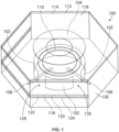
- FIG. 1 illustrates a perspective view of a ring cell 100 with an electrically conductive fence 102 ("ring fence" 102), according to some of the disclosed implementations.
- the ring cell 100 comprises a number of circuit board-based sections.
- the ring cell 100 includes a ring patch 104, two electrical feed lines 106 and 108, a ring slot 110, a top dielectric layer 112, a top adhesive layer 114, an insulating layer 116 (for example a foam layer), an upper internal adhesive layer 118, an internal metal layer 120, a middle dielectric layer 122, a lower adhesive layer 124, and a bottom dielectric layer 126.
- the foam layer 116 comprises a foam layer that separates the ring patch 104 from the ring slot 110, and is thus referred to herein as the "foam layer" 116.
- the various dielectric layers 112, 122, and 126 are printed circuit boards (PCBs).
- the ring patch 104 may be formed, etched, or adhered to the foam layer 116 to hold the ring patch 104 in place.
- the insulating layer 116 comprises a honeycomb foam.
- the electrically conductive fence 102 includes one or more metallic (or otherwise conductive) walls.
- An alternative design shown in FIG. 4 replaces the metallic walls with a circular pattern of electrical vias.
- the horizontal top section of the ring cell 100 includes the top dielectric layer 112 that supports the ring patch 104 below and also serves as an environmental shield against corrosion.
- the ring patch 104 includes a cutout hole that reduces the resonance frequency of the patch and allows a smaller outside diameter, which is desirable for mutual coupling reduction and avoidance of over-emphasis of broadside antenna gain.
- the bottom section of the ring cell 100 includes two layers of dielectric substrates, the middle dielectric layer 122 and the bottom dielectric layer 126, that collectively support the ring slot 110, dual feed lines 106 and 108, and the thin electrically conductive fence 102.
- the feed lines 106 and 108 provide electrical supply that excite orthogonal resonant modes in the ring slot 110, which, in turn excites orthogonal resonant modes in the ring patch 104 above for RF signaling.
- the electrical feed lines 106, 108 supply the electrical supply (voltage and current) to generate electrical resonance in the ring slot 110 that, then, generates the desired RF signal in the ring patch 104.
- the electrical feed lines 106, 108 receive electrical supply induced in the ring slot 110 from the ring patch 104 receiving an RF signal.
- the ring slot 110 and the ring patch 104 work together to provide a wider impedance bandwidth than either one alone could provide.
- the ring cell 100 is thus designed to operate as a hybrid radiator, working in both transmit and receive modes. Alternatively, the ring cell 100 may operate in just transmit or in just receive mode.
- the electrically conductive fence 102 shields the ring slot 110 from an RF power distribution network and reduces unwanted mutual coupling with other ring slots 110 in neighboring ring cells 100 that are part of an array antenna (e.g., a PAA).
- the diameter and depth of the electrically conductive fence 102 are set so that the ring slot 110 resonates at or near the desired operating frequency band.
- openings 128 and 130 around the electrically conductive fence 102 allow the feed lines 106 and 108 to go inside without being electrically shorted.
- the ring patch 104 and electrically conductive fence 102 are metallic or otherwise electrically conductive. Electricity is supplied to the ring cell 100 through the feed lines 106 and 108, causing the ring fence 102 and ring patch 104 to operate as a radiating element for generating specific RF signals. Shape-wise, the electrically conductive fence 102 has a larger diameter than the ring slot 110. This allows the ring slot 110 to be positioned, horizontally, inside the electrically conductive fence 102. Though, as can be seen in FIG. 2 , the ring slot 110 is positioned vertically above the electrically conductive fence 102, at least in some implementations.
- the dual electrical feed lines 106 and 108 excite orthogonal dual-linear polarizations necessary for some applications.
- a dual or single circular polarization may be required.
- some implementations include a feed structure using a T-junction divider/combiner (transmit/receive, respectively) and a 90-degree delay line for right-hand circular polarization, which is shown in FIGs. 5A and 5B .
- This integrated co-planar feed provides an economical way to achieve optimal polarization performance in the far-field.
- Left-hand circular polarization can also be realized by moving the L-shaped input line section from the current position to the other side of the V-shaped junction.
- FIGs. 6A and 6B For improved circular polarization performance over scan, other implementations use a different feed structure that uses a 90-degree hybrid coupler, which is shown in FIGs. 6A and 6B .
- the illustrated ring cells 100 disclosed herein are shaped in a hexagonal pattern. Yet, other shapes are fully contemplated as well. For instance, the ring cell 100 may be circular, rectangular, square, or the like. In these non-hexagonal shaped ring cells 100, some implementations still use a circular ring patch 104, ring slot 110, and electrically conductive fence 102.
- FIG. 2 illustrates a cut-out side view of the ring cell 100 with the electrically conductive fence 102, according to some of the disclosed implementations.
- the ring patch 104 is positioned atop the top adhesive layer 114 and below the top dielectric layer 112.
- the foam layer 116 separates the top adhesive layer 114 from the ring slot 110.
- the foam layer 116 is positioned between the top adhesive layer 114 and the upper internal adhesive layer 118.
- the ring slot 110 is situated within the internal metal layer 120.
- the electrically conductive fence 102 spans across the middle dielectric layer 122, the lower adhesive layer 124, and the bottom dielectric layer 126.
- the disclosed example shows the feed lines 106 and 108 being positioned vertically in the upper half of the electrically conductive fence 102.
- Dotted line 202 shows the vertical middle of the electrically conductive fence 102.
- the feed lines 106 and 108 are positioned in upper half 204, instead of in lower half 206.
- FIG. 3 illustrates a top view of an antenna array 300 made up of multiple ring cells 100a-d, according to some of the disclosed implementations.
- This illustration shows one example where electrical feed lines 106a-d and 108a-d of the various ring cells 100a-d with a 90-degree rotation.
- feed lines 106a and 108a are rotated 90 degrees from the positions of feed lines 106b and 108b. This positioning suppress undesirable cross-polarization signal level in the far-field.
- feed lines 106b and 108b are rotated 90 degrees from the positions of feed lines 106c and 108c.
- feed lines 106c and 108c are rotated 90 degrees from the positions of feed lines 106d and 108d.
- FIGs. 4-6B An alternative design that does not use the electrically conductive fence 102 is shown in FIGs. 4-6B . Instead of an electrically conductive fence, these alternative implementations form a circular fence using a collection of electrical vias.
- FIG. 4 illustrates a perspective view of a ring cell 400 with a circular via fence 402, according to some of the disclosed implementations.
- the ring cell 400 comprises a ring patch 404, two electrical feed lines 406 and 408, a ring slot 410, a top dielectric layer 412, a top adhesive layer 414, an insulating layer 416 (for example a foam layer), an upper internal adhesive layer 418, an internal metal layer 420, a middle dielectric layer 422, and a bottom dielectric layer 426.
- These various components are positioned in the same manner previously discussed ring cell 100.
- the ring cell 400 includes electrical vias 402a-n that are positioned in a circular pattern around the ring slot 410, collectively forming a via fence with numerous openings 430-436 (though, only four openings are labeled).
- the insulating layer 416 comprises a honeycomb foam.
- the horizontal top section of the ring cell 400 includes the top dielectric layer 412 that supports the ring patch 404 below and also serves as an environmental shield against corrosion.
- the ring patch 404 includes a cutout hole that reduces the resonance frequency of the patch and allows a smaller outside diameter, which is desirable for mutual coupling reduction and avoidance of over-emphasis of broadside antenna gain.
- the bottom section of the ring cell 400 includes two layers of dielectric substrates, the middle dielectric layer 422 and the bottom dielectric layer 426, that collectively support the ring slot 410, dual feed lines 406 and 408, and the via fence formed by the electrical vias 402a-n.
- the feed lines 406 and 408 excite orthogonal resonant modes in the ring slot 410, which, in turn excites orthogonal resonant modes in the ring patch 404 above.
- the ring slot 410 and the ring patch 404 work together to provide a wider impedance bandwidth than either one alone could provide.
- the ring cell 400 is thus designed to operate as a hybrid radiator, working in both transmit and receive modes. Alternatively, the ring cell 400 may operate in just transmit or in just receive mode.
- the ring patch 404 and electrically electrical vias 402a-n are metallic or otherwise electrically conductive. Electricity is supplied to the ring cell 400 through the feed lines 406 and 408, causing the electrical vias 402a-n and ring patch 404 to operate as a radiating element for generating specific RF signals. Shape-wise, the via fence has a larger diameter than the ring slot 410. This allows the ring slot 410 to be positioned, horizontally, inside the electrically conductive fence 402.
- the via fence created by the electrical vias 402a-n also shield the ring slot 410 from a power distribution network and reduce unwanted mutual coupling with other ring slots 410 in neighboring ring cells 400 that are part of an array antenna (e.g., a PAA).
- the diameter and depth of the via fence are set so that the ring slot 410 resonates at or near the desired operating frequency band.
- the openings around the electrical vias conductive fence 402 allow the feed lines 406 and 408 to go inside without being electrically shorted.
- the disclosed example shows the feed lines 406 and 408 being positioned vertically in the upper half of the electrical vias 402a-n.
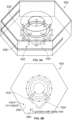
- FIGs. 5A and 5B illustrate perspective and top views, respectively, of the ring cell 400 with a T-junction delay feed line 500, according to some of the disclosed implementations.
- the T-junction delay feed line 500 includes two feed lines (shorter feed line 502 and longer L-shaped feed line 504) that extend out from a single input/output (I/O) line 506.
- Feed line 504 is longer than feed line 502 for circular polarization formation in the RF signals emitted or received through the ring cell 400. These separate feed lines 502 and 504 are positioned 90-degrees from each other. While ring cell 400 design with electrical vias 402a-n is shown, the T-junction delay feed line 500 may be used in the ring cell 100 with the electrically conductive fence 102.
- the depicted T-junction delay feed line 500 provides right-hand circular polarization, supplying optimal polarization in the far-field.
- Left-hand circular polarization may also be realized by moving the longer L-shaped feed line 504 from the illustrated position to the other side of the V-shaped junction.
- the depicted T-junction delay feed line 500 may also be used in the ring cell 100, instead of the depicted ring cell 400.
- Ring cell 400 is only shown in FIGs. 5A-5B as one example of a ring cell with the T-junction delay feed line 500.
- FIGs. 6A and 6B illustrate perspective and top views, respectively, of the ring cell 400 with a 90-degree hybrid coupler 600, according to some of the disclosed implementations.
- the hybrid coupler 600 includes two feed lines 602 and 604 and an ellipsoidal (or circular or square or rectangular) path line 606. In some implementations, feed lines 602 and 604 are positioned 90-degrees from each other.
- the hybrid coupler 600 includes two terminal ends 608 and 610. End 608 acts as an input or output of voltage supply, depending on whether the ring cell is transmitting or receiving RF signals. End 610 is connected to an electrical via 612 that spans through the bottom dielectric layer 426 and is electrically coupled to a resistor 614. In operation, this hybrid coupler 600 provides improved circular polarization performance.
- the depicted hybrid coupler 600 may also be used in the ring cell 100, instead of the depicted ring cell 400.
- Ring cell 400 is only shown in FIGs. 6A-6B as one example of a ring cell with the hybrid coupler 600.
- FIG. 7 illustrates a block diagram of an antenna system 700 for an antenna array 702 made up of the disclosed ring cells 100a-n in this disclosure.
- the antenna system 700 includes a power supply 704, a controller 706, and the antenna array 702.
- the antenna array 702 is a phased array antenna ("PAA") that includes a plurality of the ring cells 102a-n that operate either transmit and/or receive modules.
- Ring cells 100a-n include corresponding radiation elements that in combination are capable of transmitting and/or receiving RF signals.
- the ring cells 100a-n may be configured to operate within a K-band frequency range (e.g., about 20 GHz to 40 GHz for NATO K-band and 18 GHz to 26.5 GHz for IEEE K-band).
- the power supply 704 is a device, component, and/or module that provides power to the controller 706 in the antenna system 700.
- the controller 706 is a device, component, and/or module that controls the operation of the antenna array 702.
- the controller 706 may be a processor, microprocessor, microcontroller, digital signal processor ("DSP"), or other type of device that may either be programmed in hardware and/or software.
- DSP digital signal processor
- the controller 706 controls the electrical feed supplies provided to the antenna array 702, including, without limitation calibrating particular polarization, voltage, frequency, and the like of the electrical feeds. Only one line is shown between the controller 706 and the antenna array 702 for the sake of clarity, but in reality, several electrical connections and supply lines may connect the controller 706 to the antenna array 702.
- the controller 706 supplies the particular electrical feeds to the various ring cells 100a-n in order to create numerous RF signals that combine, either constructively or destructively, to form a desired cumulative RF signal for transmission.
- RF signals emitted from each ring cell 100a-n in the array antenna 702 may be in phase so as to constructively produce intense radiation or out of phase to destructively create a particular RF signal.
- Direction may be controlled by setting the phase shift between the signals sent to different ring cells 100a-n.
- the phase shift may be controlled by the controller 706 placing a slight time delay between signals sent to successive ring cells 100a-n in the array.
- the antenna system 700 is described as being in signal communication with each other, where signal communication refers to any type of communication and/or connection between the circuits, components, modules, and/or devices that allows a circuit, component, module, and/or device to pass and/or receive signals and/or information from another circuit, component, module, and/or device.
- the communication and/or connection may be along any signal path between the circuits, components, modules, and/or devices that allows signals and/or information to pass from one circuit, component, module, and/or device to another and includes wireless or wired signal paths.
- the signal paths may be physical, such as, for example, conductive wires, electromagnetic wave guides, cables, attached and/or electromagnetic or mechanically coupled terminals, semiconductive or dielectric materials or devices, or other similar physical connections or couplings. Additionally, signal paths may be non-physical such as free-space (in the case of electromagnetic propagation) or information paths through digital components where communication information is passed from one circuit, component, module, and/or device to another in varying digital formats without passing through a
- This antenna system 700 provides a means to send (or receive) RF signals to (or from) airborne / mobile vehicles with an agile electronically scanning antenna array beam without mechanical moving parts.
- the antenna system 700 can be used in communications systems and other applications, including, without limitation, for radar/sensor, electronic warfare, military applications, mobile communications, and the like.
- the antenna system 700 provides a high-performance, light-weight, low-profile and affordable solution to meet challenging and evolving mission requirements.
- FIG. 8 illustrates a perspective view of an aircraft 800 having an antenna array 702 according to various implementations of the present disclosure.
- the aircraft 800 includes a wing 802 and a wing 804 attached to a body 806.
- the aircraft 800 also includes an engine 808 attached to the wing 802 and an engine 810 attached to the wing 804.
- the body 806 has a tail section 812 with a horizontal stabilizer 814, a horizontal stabilizer 816, and a vertical stabilizer 818 attached to the tail section 812 of the body 806.
- the body 806 in some examples has a composite skin 820.
- the previously discussed antenna system 700 which includes the disclosed ring cells 100 in an antenna array 702 or just the ring cells 100 individually, may be included onto or in the aircraft 800. This is shown in FIG. 8 with a dotted box.
- the antenna system 700 may be positioned inside or outside of the aircraft 800.
- the illustration of the aircraft 800 is not meant to imply physical or architectural limitations to the manner in which an illustrative configuration may be implemented.
- the aircraft 800 is a commercial aircraft, the aircraft 800 can be a military aircraft, a rotorcraft, a helicopter, an unmanned aerial vehicle, or any other suitable aircraft.
- Other vehicles are possible as well, such as, for example but without limitation, an automobile, a motorcycle, a bus, a boat, a train, or the like.
- various examples facilitate induction welding of parts by improving the heating of (e.g., more uniformly heat) the weld interface between the parts from a single side of the parts.
- the present disclosure can be implemented using different manufacturing environments. For example, some or all aspects of the present disclosure can be implemented at least in the material procurement and component and assembly manufacturing, as described herein.
- An antenna array for communicating a radio frequency (RF) signal comprising:
- F1 An antenna array for communicating a radio frequency (RF) signal, comprising: a plurality of ring cells positioned in an antenna array, each antenna cell comprising:
- the operations illustrated in the figures may be implemented as software instructions encoded on a computer readable medium, in hardware programmed or designed to perform the operations, or both.
- aspects of the disclosure may be implemented as an ASIC, SoC, or other circuitry including a plurality of interconnected, electrically conductive elements.
Landscapes
- Physics & Mathematics (AREA)
- Electromagnetism (AREA)
- Engineering & Computer Science (AREA)
- Manufacturing & Machinery (AREA)
- Astronomy & Astrophysics (AREA)
- Aviation & Aerospace Engineering (AREA)
- General Physics & Mathematics (AREA)
- Remote Sensing (AREA)
- Waveguide Aerials (AREA)
- Variable-Direction Aerials And Aerial Arrays (AREA)
Abstract
Description
- A phased array antenna ("PAA") is a type of antenna that includes a plurality of sub-antennas (generally known as antenna elements, array elements, or radiating elements of the combined antenna) in which the relative amplitudes and phases of the respective signals feeding the array elements may be varied in a way that the effect on the total radiation pattern of the PAA is reinforced in desired directions and suppressed in undesired directions. In other words, a beam may be generated that may be pointed in or steered into different directions. Beam pointing in a transmit or receive PAA is achieved by controlling the amplitude and phase of the transmitted or received signal from each antenna element in the PAA.
- The individual radiated signals are combined to form the constructive and destructive interference patterns produced by the PAA that result in one or more antenna beams. The PAA may then be used to point the beam, or beams, rapidly in azimuth and elevation.
- The disclosed examples are described in detail below with reference to the accompanying drawing figures listed below. The following summary is provided to illustrate examples or implementations disclosed herein. It is not meant, however, to limit all examples to any particular configuration or sequence of operations.
- The disclosed examples and implementations are directed to ring cells that may be positioned together to form a larger antenna array (or PAA). The disclosed ring cells use a number stacked dielectric layers, at least two of which are separated by a low-dielectric foam layer. A horizontal top dielectric layer supports a microstrip ring patch radiator and also serves as an environmental shield against corrosion. A ring patch cutout hole reduces the resonance frequency of the patch and allows a smaller outside diameter which is desirable for mutual coupling reduction and avoidance of over-emphasis of broadside antenna gain. A lower section includes two layers of dielectric substrates to support a ring slot, dual feed lines and a thin metallic fence formed of curved metallic walls or a series of electrical vias. The feed lines excite orthogonal resonant modes in the ring slot, which, in turn excite orthogonal resonant modes in the ring patch above. The ring slot and ring patch work together to provide a wider impedance bandwidth than either one alone could provide. The ring cells may operate in transmit or receive modes.
- Other technical features may be readily apparent to one skilled in the art from the following figures, descriptions, and claims.
- For a more complete understanding of the present disclosure and its advantages, reference is now made to the following description taken in conjunction with the accompanying drawings, in which like reference numerals represent like parts:
-
FIG. 1 illustrates a perspective view of a ring cell with an electrically conductive fence, according to some of the disclosed implementations; -
FIG. 2 illustrates a cut-out side view of a ring cell with an electrically conductive fence, according to some of the disclosed implementations; -
FIG. 3 illustrates a top view of an antenna array made up of multiple ring cells, according to some of the disclosed implementations; -
FIG. 4 illustrates a perspective view of a ring cell with a circular via fence, according to some of the disclosed implementations; -
FIGs. 5A and 5B illustrate perspective and top views, respectively, of a ring cell with a T-junction delay feed line, according to some of the disclosed implementations; -
FIGs. 6A and 6B illustrate perspective and top views, respectively, of a ring cell with a 90-degree hybrid coupler, according to some of the disclosed implementations; -
FIG. 7 illustrates a block diagram of an antenna system for an antenna array made up of the disclosed ring cells in this disclosure; and -
FIG. 8 illustrates a perspective view of an aircraft having one or more array antennas made up of the disclosed ring cells in this disclosure. - Corresponding reference characters indicate corresponding parts throughout the accompanying drawings.
- The various examples will be described in detail with reference to the accompanying drawings. Wherever possible, the same reference numbers will be used throughout the drawings to refer to the same or like parts. References made throughout this disclosure relating to specific examples and implementations are provided solely for illustrative purposes but, unless indicated to the contrary, are not meant to limit all implementations.
- A phased array antenna (PAA) includes multiple emitters and is used for beamforming in high-frequency RF applications, such as in radar, 5G, or myriad other application. The number of emitters in a PAA can range from a few into the thousands. The goal in using a PAA is to control the direction of an emitted beam by exploiting constructive interference between two or more radiated signals. This is known as "beamforming" in the antenna community.
- More specifically, a PAA enables beamforming by adjusting the phase difference between the driving signal sent to each emitter in the array. This allows the radiation pattern to be controlled and directed to a target without requiring any physical movement of the antenna. This means that beamforming along a specific direction is an interference effect between quasi-omnidirectional emitters (e.g., dipole antennas).
- The disclosed implementations and examples provide a low-cost unit cell antenna element, referred to herein as a "ring cell," with unique feed structure for a PAA or other electronically scanning array. The ring cell is composed of circuit board-based sections and a foam spacer. The top section has one layer of dielectric substrate to support a microstrip ring patch radiator. The bottom section has two layers of dielectric substrates to support a ring slot, dual feed lines, and a metallic fence. The disclosed ring cells offer high-quality antenna performance over wide frequency bandwidth and large scan volume. The ring cells also provide dual-linear polarizations or circular polarizations. The disclosed ring cell does not use mechanically moving parts, eliminating much of the complexity and failure points of conventional antenna cells.
- The disclosed ring cells may be arranged in an array antenna (e.g., a PAA) that includes multiple ring cells that collectively function as an electronically scanning antenna array beam. Array antennas using the disclosed ring cells may be used in a multitude of real-world applications. For example, airplanes, motorized vehicles, various military weaponry, Internet of Things (IoT) devices, and any devices that use RF signaling may be equipped with array antennas that use the disclosed ring cells. The disclosed ring cells and antenna arrays provide electronically scanning antenna systems that dramatically reduce both integration costs due to the low-profile design and the use of affordable off-the-shelf materials.
-
FIG. 1 illustrates a perspective view of aring cell 100 with an electrically conductive fence 102 ("ring fence" 102), according to some of the disclosed implementations. Thering cell 100 comprises a number of circuit board-based sections. In addition to the electricallyconductive fence 102, thering cell 100 includes aring patch 104, twoelectrical feed lines 106 and 108, aring slot 110, a topdielectric layer 112, a topadhesive layer 114, an insulating layer 116 (for example a foam layer), an upper internaladhesive layer 118, aninternal metal layer 120, a middledielectric layer 122, a loweradhesive layer 124, and a bottomdielectric layer 126. In some implementations, thefoam layer 116 comprises a foam layer that separates thering patch 104 from thering slot 110, and is thus referred to herein as the "foam layer" 116. In some examples, the variousdielectric layers ring patch 104 may be formed, etched, or adhered to thefoam layer 116 to hold thering patch 104 in place. - In one implementation, the
insulating layer 116 comprises a honeycomb foam. - The electrically
conductive fence 102 includes one or more metallic (or otherwise conductive) walls. An alternative design shown inFIG. 4 replaces the metallic walls with a circular pattern of electrical vias. - More specifically, the horizontal top section of the
ring cell 100 includes the topdielectric layer 112 that supports thering patch 104 below and also serves as an environmental shield against corrosion. Thering patch 104 includes a cutout hole that reduces the resonance frequency of the patch and allows a smaller outside diameter, which is desirable for mutual coupling reduction and avoidance of over-emphasis of broadside antenna gain. - The bottom section of the
ring cell 100 includes two layers of dielectric substrates, themiddle dielectric layer 122 and thebottom dielectric layer 126, that collectively support thering slot 110,dual feed lines 106 and 108, and the thin electricallyconductive fence 102. The feed lines 106 and 108 provide electrical supply that excite orthogonal resonant modes in thering slot 110, which, in turn excites orthogonal resonant modes in thering patch 104 above for RF signaling. When transmitting RF signals, theelectrical feed lines 106, 108 supply the electrical supply (voltage and current) to generate electrical resonance in thering slot 110 that, then, generates the desired RF signal in thering patch 104. When receiving RF signals, theelectrical feed lines 106, 108 receive electrical supply induced in thering slot 110 from thering patch 104 receiving an RF signal. - The
ring slot 110 and thering patch 104 work together to provide a wider impedance bandwidth than either one alone could provide. Thering cell 100 is thus designed to operate as a hybrid radiator, working in both transmit and receive modes. Alternatively, thering cell 100 may operate in just transmit or in just receive mode. - The electrically
conductive fence 102 shields thering slot 110 from an RF power distribution network and reduces unwanted mutual coupling withother ring slots 110 in neighboringring cells 100 that are part of an array antenna (e.g., a PAA). The diameter and depth of the electricallyconductive fence 102 are set so that thering slot 110 resonates at or near the desired operating frequency band. In some implementations,openings conductive fence 102 allow thefeed lines 106 and 108 to go inside without being electrically shorted. - The
ring patch 104 and electricallyconductive fence 102 are metallic or otherwise electrically conductive. Electricity is supplied to thering cell 100 through thefeed lines 106 and 108, causing thering fence 102 andring patch 104 to operate as a radiating element for generating specific RF signals. Shape-wise, the electricallyconductive fence 102 has a larger diameter than thering slot 110. This allows thering slot 110 to be positioned, horizontally, inside the electricallyconductive fence 102. Though, as can be seen inFIG. 2 , thering slot 110 is positioned vertically above the electricallyconductive fence 102, at least in some implementations. - The dual
electrical feed lines 106 and 108 excite orthogonal dual-linear polarizations necessary for some applications. For other applications, a dual or single circular polarization may be required. Alternatively, some implementations include a feed structure using a T-junction divider/combiner (transmit/receive, respectively) and a 90-degree delay line for right-hand circular polarization, which is shown inFIGs. 5A and 5B . This integrated co-planar feed provides an economical way to achieve optimal polarization performance in the far-field. Left-hand circular polarization can also be realized by moving the L-shaped input line section from the current position to the other side of the V-shaped junction. For improved circular polarization performance over scan, other implementations use a different feed structure that uses a 90-degree hybrid coupler, which is shown inFIGs. 6A and 6B . - The illustrated
ring cells 100 disclosed herein are shaped in a hexagonal pattern. Yet, other shapes are fully contemplated as well. For instance, thering cell 100 may be circular, rectangular, square, or the like. In these non-hexagonal shapedring cells 100, some implementations still use acircular ring patch 104,ring slot 110, and electricallyconductive fence 102. -
FIG. 2 illustrates a cut-out side view of thering cell 100 with the electricallyconductive fence 102, according to some of the disclosed implementations. As depicted, thering patch 104 is positioned atop the topadhesive layer 114 and below thetop dielectric layer 112. Thefoam layer 116 separates the topadhesive layer 114 from thering slot 110. Specifically, thefoam layer 116 is positioned between the topadhesive layer 114 and the upper internaladhesive layer 118. Thering slot 110 is situated within theinternal metal layer 120. The electricallyconductive fence 102 spans across themiddle dielectric layer 122, the loweradhesive layer 124, and thebottom dielectric layer 126. - The disclosed example shows the
feed lines 106 and 108 being positioned vertically in the upper half of the electricallyconductive fence 102.Dotted line 202 shows the vertical middle of the electricallyconductive fence 102. As can be seen, thefeed lines 106 and 108 are positioned inupper half 204, instead of inlower half 206. -
FIG. 3 illustrates a top view of anantenna array 300 made up ofmultiple ring cells 100a-d, according to some of the disclosed implementations. This illustration shows one example whereelectrical feed lines 106a-d and 108a-d of thevarious ring cells 100a-d with a 90-degree rotation. In other words,feed lines feed lines lines feed lines lines feed lines - An alternative design that does not use the electrically
conductive fence 102 is shown inFIGs. 4-6B . Instead of an electrically conductive fence, these alternative implementations form a circular fence using a collection of electrical vias. - Along these lines,
FIG. 4 illustrates a perspective view of aring cell 400 with a circular viafence 402, according to some of the disclosed implementations. Thering cell 400 comprises aring patch 404, twoelectrical feed lines ring slot 410, atop dielectric layer 412, a topadhesive layer 414, an insulating layer 416 (for example a foam layer), an upper internaladhesive layer 418, aninternal metal layer 420, amiddle dielectric layer 422, and abottom dielectric layer 426. These various components are positioned in the same manner previously discussedring cell 100. Yet, instead of the electricallyconductive fence 102, thering cell 400 includeselectrical vias 402a-n that are positioned in a circular pattern around thering slot 410, collectively forming a via fence with numerous openings 430-436 (though, only four openings are labeled). - In one implementation, the insulating
layer 416 comprises a honeycomb foam. - Like the
ring cell 100, the horizontal top section of thering cell 400 includes thetop dielectric layer 412 that supports thering patch 404 below and also serves as an environmental shield against corrosion. Thering patch 404 includes a cutout hole that reduces the resonance frequency of the patch and allows a smaller outside diameter, which is desirable for mutual coupling reduction and avoidance of over-emphasis of broadside antenna gain. - The bottom section of the
ring cell 400 includes two layers of dielectric substrates, themiddle dielectric layer 422 and thebottom dielectric layer 426, that collectively support thering slot 410,dual feed lines ring slot 410, which, in turn excites orthogonal resonant modes in thering patch 404 above. Thering slot 410 and thering patch 404 work together to provide a wider impedance bandwidth than either one alone could provide. Thering cell 400 is thus designed to operate as a hybrid radiator, working in both transmit and receive modes. Alternatively, thering cell 400 may operate in just transmit or in just receive mode. - The
ring patch 404 and electricallyelectrical vias 402a-n are metallic or otherwise electrically conductive. Electricity is supplied to thering cell 400 through thefeed lines ring patch 404 to operate as a radiating element for generating specific RF signals. Shape-wise, the via fence has a larger diameter than thering slot 410. This allows thering slot 410 to be positioned, horizontally, inside the electricallyconductive fence 402. - The via fence created by the electrical vias 402a-n also shield the
ring slot 410 from a power distribution network and reduce unwanted mutual coupling withother ring slots 410 in neighboringring cells 400 that are part of an array antenna (e.g., a PAA). The diameter and depth of the via fence are set so that thering slot 410 resonates at or near the desired operating frequency band. In some implementations, the openings around the electrical viasconductive fence 402 allow thefeed lines - The disclosed example shows the
feed lines -
FIGs. 5A and 5B illustrate perspective and top views, respectively, of thering cell 400 with a T-junctiondelay feed line 500, according to some of the disclosed implementations. The T-junctiondelay feed line 500 includes two feed lines (shorter feed line 502 and longer L-shaped feed line 504) that extend out from a single input/output (I/O)line 506.Feed line 504 is longer thanfeed line 502 for circular polarization formation in the RF signals emitted or received through thering cell 400. Theseseparate feed lines ring cell 400 design withelectrical vias 402a-n is shown, the T-junctiondelay feed line 500 may be used in thering cell 100 with the electricallyconductive fence 102. - The depicted T-junction
delay feed line 500 provides right-hand circular polarization, supplying optimal polarization in the far-field. Left-hand circular polarization may also be realized by moving the longer L-shapedfeed line 504 from the illustrated position to the other side of the V-shaped junction. - The depicted T-junction
delay feed line 500 may also be used in thering cell 100, instead of the depictedring cell 400.Ring cell 400 is only shown inFIGs. 5A-5B as one example of a ring cell with the T-junctiondelay feed line 500. -
FIGs. 6A and 6B illustrate perspective and top views, respectively, of thering cell 400 with a 90-degree hybrid coupler 600, according to some of the disclosed implementations. The hybrid coupler 600 includes two feed lines 602 and 604 and an ellipsoidal (or circular or square or rectangular) path line 606. In some implementations, feed lines 602 and 604 are positioned 90-degrees from each other. The hybrid coupler 600 includes two terminal ends 608 and 610. End 608 acts as an input or output of voltage supply, depending on whether the ring cell is transmitting or receiving RF signals. End 610 is connected to an electrical via 612 that spans through thebottom dielectric layer 426 and is electrically coupled to a resistor 614. In operation, this hybrid coupler 600 provides improved circular polarization performance. - The depicted hybrid coupler 600 may also be used in the
ring cell 100, instead of the depictedring cell 400.Ring cell 400 is only shown inFIGs. 6A-6B as one example of a ring cell with the hybrid coupler 600. -
FIG. 7 illustrates a block diagram of anantenna system 700 for anantenna array 702 made up of the disclosedring cells 100a-n in this disclosure. In this example, theantenna system 700 includes apower supply 704, acontroller 706, and theantenna array 702. In this example, theantenna array 702 is a phased array antenna ("PAA") that includes a plurality of the ring cells 102a-n that operate either transmit and/or receive modules.Ring cells 100a-n include corresponding radiation elements that in combination are capable of transmitting and/or receiving RF signals. For example, thering cells 100a-n may be configured to operate within a K-band frequency range (e.g., about 20 GHz to 40 GHz for NATO K-band and 18 GHz to 26.5 GHz for IEEE K-band). - The
power supply 704 is a device, component, and/or module that provides power to thecontroller 706 in theantenna system 700. Thecontroller 706 is a device, component, and/or module that controls the operation of theantenna array 702. Thecontroller 706 may be a processor, microprocessor, microcontroller, digital signal processor ("DSP"), or other type of device that may either be programmed in hardware and/or software. Thecontroller 706 controls the electrical feed supplies provided to theantenna array 702, including, without limitation calibrating particular polarization, voltage, frequency, and the like of the electrical feeds. Only one line is shown between thecontroller 706 and theantenna array 702 for the sake of clarity, but in reality, several electrical connections and supply lines may connect thecontroller 706 to theantenna array 702. - In some implementations, the
controller 706 supplies the particular electrical feeds to thevarious ring cells 100a-n in order to create numerous RF signals that combine, either constructively or destructively, to form a desired cumulative RF signal for transmission. - RF signals emitted from each
ring cell 100a-n in thearray antenna 702 may be in phase so as to constructively produce intense radiation or out of phase to destructively create a particular RF signal. Direction may be controlled by setting the phase shift between the signals sent todifferent ring cells 100a-n. The phase shift may be controlled by thecontroller 706 placing a slight time delay between signals sent tosuccessive ring cells 100a-n in the array. - The
antenna system 700 is described as being in signal communication with each other, where signal communication refers to any type of communication and/or connection between the circuits, components, modules, and/or devices that allows a circuit, component, module, and/or device to pass and/or receive signals and/or information from another circuit, component, module, and/or device. The communication and/or connection may be along any signal path between the circuits, components, modules, and/or devices that allows signals and/or information to pass from one circuit, component, module, and/or device to another and includes wireless or wired signal paths. The signal paths may be physical, such as, for example, conductive wires, electromagnetic wave guides, cables, attached and/or electromagnetic or mechanically coupled terminals, semiconductive or dielectric materials or devices, or other similar physical connections or couplings. Additionally, signal paths may be non-physical such as free-space (in the case of electromagnetic propagation) or information paths through digital components where communication information is passed from one circuit, component, module, and/or device to another in varying digital formats without passing through a direct electromagnetic connection. - This
antenna system 700 provides a means to send (or receive) RF signals to (or from) airborne / mobile vehicles with an agile electronically scanning antenna array beam without mechanical moving parts. Theantenna system 700 can be used in communications systems and other applications, including, without limitation, for radar/sensor, electronic warfare, military applications, mobile communications, and the like. Theantenna system 700 provides a high-performance, light-weight, low-profile and affordable solution to meet challenging and evolving mission requirements. -
FIG. 8 illustrates a perspective view of anaircraft 800 having anantenna array 702 according to various implementations of the present disclosure. Theaircraft 800 includes awing 802 and awing 804 attached to abody 806. Theaircraft 800 also includes anengine 808 attached to thewing 802 and anengine 810 attached to thewing 804. Thebody 806 has atail section 812 with ahorizontal stabilizer 814, ahorizontal stabilizer 816, and avertical stabilizer 818 attached to thetail section 812 of thebody 806. Thebody 806 in some examples has acomposite skin 820. - In some examples, the previously discussed
antenna system 700, which includes the disclosedring cells 100 in anantenna array 702 or just thering cells 100 individually, may be included onto or in theaircraft 800. This is shown inFIG. 8 with a dotted box. Theantenna system 700 may be positioned inside or outside of theaircraft 800. - The illustration of the
aircraft 800 is not meant to imply physical or architectural limitations to the manner in which an illustrative configuration may be implemented. For example, although theaircraft 800 is a commercial aircraft, theaircraft 800 can be a military aircraft, a rotorcraft, a helicopter, an unmanned aerial vehicle, or any other suitable aircraft. Other vehicles are possible as well, such as, for example but without limitation, an automobile, a motorcycle, a bus, a boat, a train, or the like. - Thus, various examples facilitate induction welding of parts by improving the heating of (e.g., more uniformly heat) the weld interface between the parts from a single side of the parts. The present disclosure, including the examples described herein, can be implemented using different manufacturing environments. For example, some or all aspects of the present disclosure can be implemented at least in the material procurement and component and assembly manufacturing, as described herein.
- The following clauses describe further aspects of the present disclosure. In some implementations, the clauses described below can be further combined in any sub-combination without departing from the scope of the present disclosure.
- Clause Set A:
- A1: A ring cell for generating a radio frequency (RF) signal, the ring cell comprising:
- a plurality of dielectric layers comprising a top dielectric layer, a middle dielectric layer, and a bottom dielectric layer;
- a ring patch positioned in the top dielectric layer;
- a foam layer between the top dielectric layer and the middle dielectric layer;
- a ring slot position between the foam layer and the middle dielectric layer;
- an electrically conductive fence positioned below and supporting the ring slot, the electrically conductive fence spanning through the bottom dielectric layer; and
- electrical feed lines supplying electrical feed to generate electrical resonance in the ring slot for producing the RF signal in the ring patch.
- A2: The ring cell of claim A1, wherein the plurality of dielectric layers comprise one or more printed circuit boards.
- A3: The ring cell of claims A1 or A2, wherein the electrical feed lines are co-planar to the electrically conductive fence in an upper half of the electrically conductive fence toward the top dielectric layer.
- A4: The ring cell of any of claims A1-A3, further comprising a plurality of adhesives that are affixed to the plurality of dielectric layers.
- A5: The ring cell of any of claims A1-A4, wherein the ring patch is positioned below the top dielectric layer and above the foam layer.
- A6: The ring cell of any of claims A1-A5, wherein the foam layer comprises a honeycomb foam.
- Clause Set B:
- B1: A ring cell for generating or receiving a radio frequency (RF) signal, the ring cell comprising:
- a plurality of dielectric layers comprising a top dielectric layer, a middle dielectric layer, and a bottom dielectric layer;
- a ring patch positioned in the top dielectric layer;
- a foam layer between the top dielectric layer and the middle dielectric layer;
- a ring slot position between the foam layer and the middle dielectric layer;
- an electrically conductive fence positioned below and supporting the ring slot, the electrically conductive fence spanning through the bottom dielectric layer; and
- a T-junction delay feed line for supplying electrical feed to generate electrical resonance in the ring slot for producing the RF signal in the ring patch.
- B2: The ring cell of claim B1, wherein the T-junction delay feed line comprises an L-shaped feed line and a second feed line.
- B3: The ring cell of claim B2, wherein the L-shaped feed line is longer than the second feed line.
- B4: The ring cell of claims B2 or B3, wherein the L-shaped feed line and the second feed line extend from a single feed line.
- B5: The ring cell of claim B4, wherein the foam layer comprises a honeycomb foam.
- B6: The ring cell of claim B1, wherein the ring patch is positioned below the top dielectric layer and above the foam layer.
- B7: The ring cell of claims B1 or B6, wherein the ring patch is attached to an adhesive layer atop the foam layer.
- Clause Set C:
- C1: A ring cell for generating or receiving a radio frequency (RF) signal, the ring cell comprising:
- a plurality of dielectric layers comprising a top dielectric layer, a middle dielectric layer, and a bottom dielectric layer;
- a ring patch positioned in the top dielectric layer;
- a foam layer between the top dielectric layer and the middle dielectric layer;
- a ring slot position between the foam layer and the middle dielectric layer; and
- an electrically conductive fence positioned below and supporting the ring slot, the electrically conductive fence spanning through the bottom dielectric layer; and
- a hybrid coupler for supplying electrical feed to generate electrical resonance in the ring slot for producing the RF signal in the ring patch.
- C2: The ring cell of claim C1, wherein the hybrid coupler comprises two feed lines and an ellipsoidal feed path line.
- C3: The ring cell of claim C2, wherein the hybrid coupler comprises two feed lines and a circular feed path line.
- C4: The ring cell of claim C2, wherein the hybrid coupler comprises an electrical via that extends through the bottom dielectric layer and is electrically coupled to a resistor.
- Clause Set D:
- D1: A ring cell for receiving radio frequency (RF) signal, the ring cell comprising:
- a plurality of dielectric layers comprising a top dielectric layer, a middle dielectric layer, and a bottom dielectric layer;
- a ring patch positioned in the top dielectric layer for receiving the RF signal;
- a foam layer between the top dielectric layer and the middle dielectric layer;
- a ring slot position between the foam layer and the middle dielectric layer, wherein the ring slot being positioned to electromagnetically receive the RF signal from the ring patch; and electrical feed lines positioned to output the RF signal received by the ring slot as an output.
- D2: The ring cell of claim D2, further comprising an electrically conductive fence positioned below and supporting the ring slot, the electrically conductive fence spanning through the bottom dielectric layer.
- D3: The ring cell of claim D1, further comprising a plurality of electrical vias extending through the bottom dielectric layer.
- D4: The ring cell claim 18, wherein the electrical feed lines are rotated 90-degrees from other electrical feed lines of a neighboring ring cell in an antenna array.
- Clause Set E:
E1: An antenna array for communicating a radio frequency (RF) signal, comprising: - a plurality of ring cells positioned in an array, each antenna cell comprising:
- a plurality of dielectric layers comprising a top dielectric layer, a middle dielectric layer, and a bottom dielectric layer;
- a ring patch positioned in the top dielectric layer;
- a foam layer between the top dielectric layer and the middle dielectric layer;
- a ring slot position between the foam layer and the middle dielectric layer;
- an electrically conductive fence positioned below and supporting the ring slot, the electrically conductive fence spanning through the bottom dielectric layer; and
- electrical feed lines supplying electrical feed to generate electrical resonance in the ring slot for producing the RF signal in the ring patch.
- Clause Set F:
F1: An antenna array for communicating a radio frequency (RF) signal, comprising:
a plurality of ring cells positioned in an antenna array, each antenna cell comprising: - a plurality of dielectric layers comprising a top dielectric layer, a middle dielectric layer, and a bottom dielectric layer;
- a ring patch positioned in the top dielectric layer for receiving the RF signal;
- a foam layer between the top dielectric layer and the middle dielectric layer;
- a ring slot position between the foam layer and the middle dielectric layer, wherein the ring slot being positioned to electromagnetically receive the RF signal from the ring patch; and
- electrical feed lines positioned to output the RF signal received by the ring slot as an output.
- Clause Set G:
- G1: A ring cell for generating a radio frequency (RF) signal, the ring cell comprising:
- a plurality of dielectric layers comprising a top dielectric layer, a middle dielectric layer, and a bottom dielectric layer;
- a ring patch positioned in the top dielectric layer;
- a foam layer between the top dielectric layer and the middle dielectric layer;
- a ring slot position between the foam layer and the middle dielectric layer; and
- electrical feed lines supplying electrical feed to generate electrical resonance in the ring slot for producing the RF signal in the ring patch.
- G2: The ring cell of claim G1, further comprising an electrically conductive fence positioned below and supporting the ring slot, the electrically conductive fence spanning through the bottom dielectric layer
- G3: The ring cell of claim G1, further comprising a plurality of electrical vias extending through the bottom dielectric layer.
- Although the subject matter has been described in language specific to structural features and/or methodological acts, it is to be understood that the subject matter defined in the appended claims is not necessarily limited to the specific features or acts described above. Rather, the specific features and acts described above are disclosed as example forms of implementing the claims.
- It will be understood that the benefits and advantages described above may relate to one implementation or may relate to several implementations. The implementations are not limited to those that solve any or all of the stated problems or those that have any or all of the stated benefits and advantages. It will further be understood that reference to 'an' item refers to one or more of those items.
- The term "comprising" is used in this disclosure to mean including the feature(s) or act(s) followed thereafter, without excluding the presence of one or more additional features or acts.
- In some examples, the operations illustrated in the figures may be implemented as software instructions encoded on a computer readable medium, in hardware programmed or designed to perform the operations, or both. For example, aspects of the disclosure may be implemented as an ASIC, SoC, or other circuitry including a plurality of interconnected, electrically conductive elements.
- The order of execution or performance of the operations in examples of the disclosure illustrated and described herein is not essential, unless otherwise specified. That is, the operations may be performed in any order, unless otherwise specified, and examples of the disclosure may include additional or fewer operations than those disclosed herein. For example, it is contemplated that executing or performing a particular operation before, contemporaneously with, or after another operation is within the scope of aspects of the disclosure.
- When introducing elements of aspects of the disclosure or the examples thereof, the articles "a," "an," "the," and "said" are intended to mean that there are one or more of the elements. The terms "comprising," "including," and "having" are intended to be inclusive and mean that there may be additional elements other than the listed elements. The term "exemplary" is intended to mean "an example of." The phrase "one or more of the following: A, B, and C" means "at least one of A and/or at least one of B and/or at least one of C."
- Having described aspects of the disclosure in detail, it will be apparent that modifications and variations are possible without departing from the scope of aspects of the disclosure as defined in the appended claims. As various changes could be made in the above constructions, products, and methods without departing from the scope of aspects of the disclosure, it is intended that all matter contained in the above description and shown in the accompanying drawings shall be interpreted as illustrative and not in a limiting sense.
- It is to be understood that the above description is intended to be illustrative, and not restrictive. As an illustration, the above-described implementations (and/or aspects thereof) are usable in combination with each other. In addition, many modifications are practicable to adapt a particular situation or material to the teachings of the various implementations of the disclosure without departing from their scope. While the dimensions and types of materials described herein are intended to define the parameters of the various implementations of the disclosure, the implementations are by no means limiting and are exemplary implementations. Many other implementations will be apparent to those of ordinary skill in the art upon reviewing the above description. The scope of the various implementations of the disclosure should, therefore, be determined with reference to the appended claims, along with the full scope of equivalents to which such claims are entitled. In the appended claims, the terms "including" and "in which" are used as the plain-English equivalents of the respective terms "comprising" and "wherein." Further, the limitations of the following claims are not written in means-plus-function format and are not intended to be interpreted based on 35 U.S.C. § 112(f), unless and until such claim limitations expressly use the phrase "means for" followed by a statement of function void of further structure.
- This written description uses examples to disclose the various implementations of the disclosure, including the best mode, and also to enable any person of ordinary skill in the art to practice the various implementations of the disclosure, including making and using any devices or systems and performing any incorporated methods. The patentable scope of the various implementations of the disclosure is defined by the claims, and includes other examples that occur to those persons of ordinary skill in the art. Such other examples are intended to be within the scope of the claims if the examples have structural elements that do not differ from the literal language of the claims, or if the examples include equivalent structural elements with insubstantial differences from the literal language of the claims.
- Although the present disclosure has been described with reference to various implementations, various changes and modifications can be made without departing from the scope of the present disclosure.
Claims (15)
- A ring cell (100) for generating radio frequency, RF, signal, the ring cell (100) comprising:a plurality of dielectric layers comprising a top dielectric layer (112), a middle dielectric layer (122), and a bottom dielectric layer (126);a ring patch (104) positioned in the top dielectric layer (112);an insulating layer (116) between the top dielectric layer (112) and the middle dielectric layer (122);a ring slot (110) positioned between the insulating layer (116) and the middle dielectric layer (122);an electrically conductive fence (102) positioned below and supporting the ring slot (110), the electrically conductive fence (102) spanning through the bottom dielectric layer (126); andelectrical feed lines (106, 108) supplying electrical feed to generate electrical resonance in the ring slot for (110) producing the RF signal in the ring patch (104).
- The ring cell (100) of claim 1, wherein the dielectric layers (112, 122, 126) comprise one or more printed circuit boards.
- The ring cell (100) of claims 1 or 2, wherein the electrical feed lines (106, 108) are co-planar to the electrically conductive fence (102) in an upper half (204) of the electrically conductive fence (102) toward the top dielectric layer (112).
- The ring cell (100) of any of claims 1-3, further comprising at plurality of adhesive layers (114, 118, 124) that are affixed to the plurality of dielectric layers (112, 122, 126).
- The ring cell (100) of any of claims 1-4, wherein the ring patch (104) is positioned below the top dielectric layer (112) and above the insulating layer (116).
- The ring cell (100) of any of claims 1-5, wherein the insulating layer (116) comprises a honeycomb foam.
- A ring cell (100; 400) for generating or receiving radio frequency ,RF, signal, the ring cell (100; 400) comprising:a plurality of dielectric layers comprising a top dielectric layer (112; 412), a middle dielectric layer (122; 422), and a bottom dielectric layer (126; 426);a ring patch (104; 404) positioned in the top dielectric layer (112; 412);an insulating layer (116; 416) between the top dielectric layer (112; 412) and the middle dielectric layer (122; 422);a ring slot (110; 410) positioned between the insulating layer (116; 416) and the middle dielectric layer (122; 422);an electrically conductive fence (102; 402) positioned below and supporting the ring slot (110; 410), the electrically conductive fence (102; 402) spanning through the bottom dielectric layer (126; 426); anda hybrid coupler (600) for supplying electrical feed to generate electrical resonance in the ring slot (110; 410) for producing the RF signal in the ring patch (104; 404).
- The ring cell (100; 400) of claim 7, wherein the hybrid coupler (600) comprises an L-shaped feed line (504) and a second feed line (502).
- The ring cell (100; 400) of claim 8, wherein the L-shaped feed line (504) is longer than the second feed line (502).
- The ring cell (100; 400) of claims 8 or 9, wherein the L-shaped feed line (504) and the second feed line (502) extend from a single feed line (506).
- The ring cell (100; 400) of claim 7, wherein the insulating layer (116; 416) comprises a honeycomb foam.
- The ring cell (100; 400) of claims 7 or 11, wherein the ring patch (104; 404) is positioned below the top dielectric layer (112; 412) and above the insulating layer (116; 416).
- The ring cell (100; 400) of claims 7 or 11, wherein the ring patch (140; 404) is attached to an adhesive layer atop the insulating layer (116; 426).
- The ring cell (100; 400) of claim 7, wherein the hybrid coupler (600) comprises two feed lines (602, 604) and a square or rectangular feed path line (606).
- The ring cell (100; 400) of claim 7, wherein the hybrid coupler (600) comprises two feed lines (602, 604) and an ellipsoidal feed path line (606).
Applications Claiming Priority (2)
| Application Number | Priority Date | Filing Date | Title |
|---|---|---|---|
| US202163251528P | 2021-10-01 | 2021-10-01 | |
| US17/588,159 US12176635B2 (en) | 2021-10-01 | 2022-01-28 | Ring slot patch radiator unit cell for phased array antennas |
Publications (1)
| Publication Number | Publication Date |
|---|---|
| EP4160819A1 true EP4160819A1 (en) | 2023-04-05 |
Family
ID=83438673
Family Applications (1)
| Application Number | Title | Priority Date | Filing Date |
|---|---|---|---|
| EP22197111.2A Pending EP4160819A1 (en) | 2021-10-01 | 2022-09-22 | Ring slot patch radiator unit cell for phased array antennas |
Country Status (3)
| Country | Link |
|---|---|
| US (1) | US12176635B2 (en) |
| EP (1) | EP4160819A1 (en) |
| CN (1) | CN115939742A (en) |
Cited By (1)
| Publication number | Priority date | Publication date | Assignee | Title |
|---|---|---|---|---|
| CN119133828A (en) * | 2023-12-21 | 2024-12-13 | 南通大学 | A wide beam dielectric resonator antenna |
Citations (3)
| Publication number | Priority date | Publication date | Assignee | Title |
|---|---|---|---|---|
| US5055852A (en) * | 1989-06-20 | 1991-10-08 | Alcatel Espace | Diplexing radiating element |
| US20150084814A1 (en) * | 2012-03-14 | 2015-03-26 | Israel Aerospace Industries Ltd. | Phased array antenna |
| US20180191073A1 (en) * | 2016-12-29 | 2018-07-05 | Trimble Inc. | Circularly Polarized Connected-Slot Antennas |
Family Cites Families (21)
| Publication number | Priority date | Publication date | Assignee | Title |
|---|---|---|---|---|
| US6369759B1 (en) * | 1999-06-09 | 2002-04-09 | California Institute Of Technology | Rectenna for high-voltage applications |
| US6281857B1 (en) * | 1999-12-23 | 2001-08-28 | Zenith Electronics Corporation | Dipole UHF antenna |
| WO2003034545A1 (en) * | 2001-10-16 | 2003-04-24 | Fractus, S.A. | Multifrequency microstrip patch antenna with parasitic coupled elements |
| JP3420233B2 (en) * | 2001-11-28 | 2003-06-23 | 日本アンテナ株式会社 | Composite antenna |
| US8368596B2 (en) * | 2004-09-24 | 2013-02-05 | Viasat, Inc. | Planar antenna for mobile satellite applications |
| JP2008515253A (en) * | 2004-09-24 | 2008-05-08 | ジャスト・サール | Planar antenna for mobile satellite applications |
| US7671696B1 (en) * | 2006-09-21 | 2010-03-02 | Raytheon Company | Radio frequency interconnect circuits and techniques |
| US8350771B1 (en) * | 2009-06-02 | 2013-01-08 | The United States Of America, As Represented By The Secretary Of The Navy | Dual-band dual-orthogonal-polarization antenna element |
| US8773323B1 (en) * | 2011-03-18 | 2014-07-08 | The Boeing Company | Multi-band antenna element with integral faraday cage for phased arrays |
| US8749446B2 (en) * | 2011-07-29 | 2014-06-10 | The Boeing Company | Wide-band linked-ring antenna element for phased arrays |
| US20150303576A1 (en) * | 2012-11-21 | 2015-10-22 | Eseo | Miniaturized Patch Antenna |
| US9130278B2 (en) * | 2012-11-26 | 2015-09-08 | Raytheon Company | Dual linear and circularly polarized patch radiator |
| US9819088B2 (en) * | 2014-12-09 | 2017-11-14 | City University Of Hong Kong | Aperture-coupled microstrip-line feed for circularly polarized patch antenna |
| US9742058B1 (en) * | 2015-08-06 | 2017-08-22 | Gregory A. O'Neill, Jr. | Deployable quadrifilar helical antenna |
| US10686258B2 (en) * | 2017-09-18 | 2020-06-16 | Integrated Device Technology, Inc. | Hard-wired address for phased array antenna panels |
| JP7137330B2 (en) * | 2018-03-20 | 2022-09-14 | 株式会社東芝 | antenna device |
| US11456534B2 (en) * | 2018-07-12 | 2022-09-27 | The United States Of America As Represented By The Secretary Of The Army | Broadband stacked parasitic geometry for a multi-band and dual polarization antenna |
| JP7107105B2 (en) * | 2018-08-30 | 2022-07-27 | Tdk株式会社 | antenna |
| CN111834731B (en) * | 2019-04-19 | 2022-03-01 | Oppo广东移动通信有限公司 | Antenna module and electronic equipment |
| CN110212300B (en) * | 2019-05-22 | 2021-05-11 | 维沃移动通信有限公司 | An antenna unit and terminal equipment |
| US11322833B2 (en) * | 2019-06-03 | 2022-05-03 | Space Exploration Technologies Corp. | Antenna apparatus having fastener system |
-
2022
- 2022-01-28 US US17/588,159 patent/US12176635B2/en active Active
- 2022-09-22 EP EP22197111.2A patent/EP4160819A1/en active Pending
- 2022-09-28 CN CN202211189865.8A patent/CN115939742A/en active Pending
Patent Citations (3)
| Publication number | Priority date | Publication date | Assignee | Title |
|---|---|---|---|---|
| US5055852A (en) * | 1989-06-20 | 1991-10-08 | Alcatel Espace | Diplexing radiating element |
| US20150084814A1 (en) * | 2012-03-14 | 2015-03-26 | Israel Aerospace Industries Ltd. | Phased array antenna |
| US20180191073A1 (en) * | 2016-12-29 | 2018-07-05 | Trimble Inc. | Circularly Polarized Connected-Slot Antennas |
Cited By (1)
| Publication number | Priority date | Publication date | Assignee | Title |
|---|---|---|---|---|
| CN119133828A (en) * | 2023-12-21 | 2024-12-13 | 南通大学 | A wide beam dielectric resonator antenna |
Also Published As
| Publication number | Publication date |
|---|---|
| US20240170851A1 (en) | 2024-05-23 |
| CN115939742A (en) | 2023-04-07 |
| US12176635B2 (en) | 2024-12-24 |
Similar Documents
| Publication | Publication Date | Title |
|---|---|---|
| US12266862B2 (en) | Ultra-low-cost 1D-scanning antenna array | |
| CN110391495B (en) | Phased array antenna and method of manufacturing printed circuit board unit cell | |
| US4812855A (en) | Dipole antenna with parasitic elements | |
| US10283876B1 (en) | Dual-polarized, planar slot-aperture antenna element | |
| Mahfuz et al. | Review of patch antennas used in drone applications | |
| US20250210860A1 (en) | Low cost electronically scanning antenna array architecture | |
| US10978812B2 (en) | Single layer shared aperture dual band antenna | |
| US6307510B1 (en) | Patch dipole array antenna and associated methods | |
| US20260051658A1 (en) | High isolation ring slot patch radiator for phased array antennas | |
| EP4160819A1 (en) | Ring slot patch radiator unit cell for phased array antennas | |
| Reis et al. | General Overview of Antennas for Unmanned Aerial Vehicles: A Review | |
| US12021305B1 (en) | Conformal antenna system | |
| EP4228096B1 (en) | Unit cell antenna for phased arrays | |
| Chu et al. | Coding metasurface integrated dual-band antenna for vehicular communications | |
| WO2013039570A1 (en) | A dual polarization antenna with high port isolation | |
| EP4576420A1 (en) | High isolation ring slot patch radiator for phased array antennas | |
| US11038273B1 (en) | Electronically scanning antenna assembly | |
| CN116073128A (en) | A Wing Conformal End-Fire Phased Array Antenna Based on Pattern Optimization of Array Elements | |
| Wu et al. | A Beam-Switching Planar Antenna Module with 360° In-Plane Coverage for Drone Collision Avoidance Radar | |
| US12316013B1 (en) | Ultra-broadband current sheet array | |
| Haykir et al. | Compact and Directional Printed Dipole Antenna Pair Conformed on a Conical Surface | |
| CN118448865B (en) | Low-profile circularly polarized end-fire antenna | |
| US20250007178A1 (en) | Low profile, high power microwave antenna, combiner and radial waveguide and additive manufacture of same | |
| CN119890673A (en) | Microstrip magneto-electric control two-dimensional beam scanning antenna | |
| JPH08130407A (en) | Polarizing angle and orientated direction control antenna |
Legal Events
| Date | Code | Title | Description |
|---|---|---|---|
| PUAI | Public reference made under article 153(3) epc to a published international application that has entered the european phase |
Free format text: ORIGINAL CODE: 0009012 |
|
| STAA | Information on the status of an ep patent application or granted ep patent |
Free format text: STATUS: THE APPLICATION HAS BEEN PUBLISHED |
|
| AK | Designated contracting states |
Kind code of ref document: A1 Designated state(s): AL AT BE BG CH CY CZ DE DK EE ES FI FR GB GR HR HU IE IS IT LI LT LU LV MC MK MT NL NO PL PT RO RS SE SI SK SM TR |
|
| STAA | Information on the status of an ep patent application or granted ep patent |
Free format text: STATUS: REQUEST FOR EXAMINATION WAS MADE |
|
| 17P | Request for examination filed |
Effective date: 20230901 |
|
| RBV | Designated contracting states (corrected) |
Designated state(s): AL AT BE BG CH CY CZ DE DK EE ES FI FR GB GR HR HU IE IS IT LI LT LU LV MC MK MT NL NO PL PT RO RS SE SI SK SM TR |
|
| GRAP | Despatch of communication of intention to grant a patent |
Free format text: ORIGINAL CODE: EPIDOSNIGR1 |
|
| STAA | Information on the status of an ep patent application or granted ep patent |
Free format text: STATUS: GRANT OF PATENT IS INTENDED |
|
| RIC1 | Information provided on ipc code assigned before grant |
Ipc: H01Q 9/04 20060101AFI20251002BHEP Ipc: H01Q 1/28 20060101ALI20251002BHEP Ipc: H01Q 3/28 20060101ALI20251002BHEP Ipc: H01Q 3/38 20060101ALI20251002BHEP Ipc: H01Q 21/06 20060101ALI20251002BHEP |
|
| INTG | Intention to grant announced |
Effective date: 20251103 |
|
| GRAJ | Information related to disapproval of communication of intention to grant by the applicant or resumption of examination proceedings by the epo deleted |
Free format text: ORIGINAL CODE: EPIDOSDIGR1 |
|
| STAA | Information on the status of an ep patent application or granted ep patent |
Free format text: STATUS: REQUEST FOR EXAMINATION WAS MADE |
|
| GRAP | Despatch of communication of intention to grant a patent |
Free format text: ORIGINAL CODE: EPIDOSNIGR1 |
|
| STAA | Information on the status of an ep patent application or granted ep patent |
Free format text: STATUS: GRANT OF PATENT IS INTENDED |
|
| INTC | Intention to grant announced (deleted) | ||
| INTG | Intention to grant announced |
Effective date: 20260312 |