EP4160816A1 - Ultra-low-cost 1d-scanning antenna array - Google Patents
Ultra-low-cost 1d-scanning antenna array Download PDFInfo
- Publication number
- EP4160816A1 EP4160816A1 EP22196914.0A EP22196914A EP4160816A1 EP 4160816 A1 EP4160816 A1 EP 4160816A1 EP 22196914 A EP22196914 A EP 22196914A EP 4160816 A1 EP4160816 A1 EP 4160816A1
- Authority
- EP
- European Patent Office
- Prior art keywords
- square ring
- antenna element
- dielectric layer
- antenna
- dielectric
- Prior art date
- Legal status (The legal status is an assumption and is not a legal conclusion. Google has not performed a legal analysis and makes no representation as to the accuracy of the status listed.)
- Pending
Links
Images




Classifications
-
- H—ELECTRICITY
- H01—ELECTRIC ELEMENTS
- H01Q—ANTENNAS, i.e. RADIO AERIALS
- H01Q1/00—Details of, or arrangements associated with, antennas
- H01Q1/27—Adaptation for use in or on movable bodies
- H01Q1/28—Adaptation for use in or on aircraft, missiles, satellites, or balloons
- H01Q1/286—Adaptation for use in or on aircraft, missiles, satellites, or balloons substantially flush mounted with the skin of the craft
-
- H—ELECTRICITY
- H01—ELECTRIC ELEMENTS
- H01Q—ANTENNAS, i.e. RADIO AERIALS
- H01Q21/00—Antenna arrays or systems
- H01Q21/06—Arrays of individually energised antenna units similarly polarised and spaced apart
- H01Q21/061—Two dimensional planar arrays
- H01Q21/065—Patch antenna array
-
- H—ELECTRICITY
- H01—ELECTRIC ELEMENTS
- H01Q—ANTENNAS, i.e. RADIO AERIALS
- H01Q15/00—Devices for reflection, refraction, diffraction or polarisation of waves radiated from an antenna, e.g. quasi-optical devices
- H01Q15/14—Reflecting surfaces; Equivalent structures
- H01Q15/141—Apparatus or processes specially adapted for manufacturing reflecting surfaces
- H01Q15/142—Apparatus or processes specially adapted for manufacturing reflecting surfaces using insulating material for supporting the reflecting surface
- H01Q15/144—Apparatus or processes specially adapted for manufacturing reflecting surfaces using insulating material for supporting the reflecting surface with a honeycomb, cellular or foamed sandwich structure
-
- H—ELECTRICITY
- H01—ELECTRIC ELEMENTS
- H01Q—ANTENNAS, i.e. RADIO AERIALS
- H01Q9/00—Electrically-short antennas having dimensions not more than twice the operating wavelength and consisting of conductive active radiating elements
- H01Q9/04—Resonant antennas
- H01Q9/0407—Substantially flat resonant element parallel to ground plane, e.g. patch antenna
- H01Q9/0414—Substantially flat resonant element parallel to ground plane, e.g. patch antenna in a stacked or folded configuration
-
- H—ELECTRICITY
- H01—ELECTRIC ELEMENTS
- H01Q—ANTENNAS, i.e. RADIO AERIALS
- H01Q9/00—Electrically-short antennas having dimensions not more than twice the operating wavelength and consisting of conductive active radiating elements
- H01Q9/04—Resonant antennas
- H01Q9/0407—Substantially flat resonant element parallel to ground plane, e.g. patch antenna
- H01Q9/0428—Substantially flat resonant element parallel to ground plane, e.g. patch antenna radiating a circular polarised wave
- H01Q9/0435—Substantially flat resonant element parallel to ground plane, e.g. patch antenna radiating a circular polarised wave using two feed points
-
- H—ELECTRICITY
- H01—ELECTRIC ELEMENTS
- H01Q—ANTENNAS, i.e. RADIO AERIALS
- H01Q9/00—Electrically-short antennas having dimensions not more than twice the operating wavelength and consisting of conductive active radiating elements
- H01Q9/04—Resonant antennas
- H01Q9/0407—Substantially flat resonant element parallel to ground plane, e.g. patch antenna
- H01Q9/045—Substantially flat resonant element parallel to ground plane, e.g. patch antenna with particular feeding means
- H01Q9/0457—Substantially flat resonant element parallel to ground plane, e.g. patch antenna with particular feeding means electromagnetically coupled to the feed line
-
- H—ELECTRICITY
- H01—ELECTRIC ELEMENTS
- H01Q—ANTENNAS, i.e. RADIO AERIALS
- H01Q9/00—Electrically-short antennas having dimensions not more than twice the operating wavelength and consisting of conductive active radiating elements
- H01Q9/04—Resonant antennas
- H01Q9/0407—Substantially flat resonant element parallel to ground plane, e.g. patch antenna
- H01Q9/0464—Annular ring patch
Definitions
- a phased array antenna is a type of antenna that includes a plurality of sub-antennas (generally known as antenna elements, array elements, or radiating elements of the combined antenna) in which the relative amplitudes and phases of the respective signals feeding the array elements may be varied in a way that the effect on the total radiation pattern of the PAA is reinforced in desired directions and suppressed in undesired directions.
- a beam may be generated that may be pointed in or steered into different directions. Beam pointing in a transmit or receive PAA is achieved by controlling the amplitude and phase of the transmitted or received signal from each antenna element in the PAA.
- the individual radiated signals are combined to form the constructive and destructive interference patterns produced by the PAA that result in one or more antenna beams.
- the PAA may then be used to point the beam, or beams, rapidly in azimuth and elevation.
- the disclosed examples and implementations are directed to antenna elements that may be positioned together to form an antenna array (or PAA), which may be affixed or incorporated in curved or conformal structures (e.g., aircraft bodies).
- the disclosed antenna elements use a number of stacked dielectric layers, at least two of which are separated by a low-dielectric foam layer, such as a core or low-dielectric foam or honeycomb material with low average dielectric constant structure.
- a horizontal top dielectric layer supports a microstrip square ring patch radiator and also serves as an environmental shield against corrosion.
- a square ring patch cutout hole reduces the resonance frequency of the patch and allows a smaller outside diameter which is desirable for mutual coupling reduction and avoidance of over-emphasis of broadside antenna gain.
- a lower section includes two layers of dielectric substrates to support a square ring slot and feed lines (e.g., single line providing single linear polarization or dual feed lines providing dual linear polarization) for providing RF power or carrying away received RF signals.
- the feed lines excite orthogonal resonant modes in the square ring slot, which, in turn excite orthogonal resonant modes in the square ring patch above.
- the square ring slot and square ring patch work together to provide a wider impedance bandwidth than either one alone could provide.
- the antenna elements may operate in transmit or receive RF modes.
- a phased array antenna includes multiple emitters and is used for beamforming in high-frequency RF applications, such as in radar, 5G, or myriad other application.
- the number of emitters in a PAA can range from a few into the thousands.
- the goal in using a PAA is to control the direction of an emitted beam by exploiting constructive interference between two or more radiated signals. This is known as "beamforming" in the antenna community.
- a PAA enables beamforming by adjusting the phase difference between the driving signal sent to each emitter in the array. This allows the radiation pattern to be controlled and directed to a target without requiring any physical movement of the antenna. This means that beamforming along a specific direction is an interference effect between quasi-omnidirectional emitters (e.g., dipole antennas).
- the disclosed implementations and examples provide an ultra-low-cost unit cell antenna element with unique feed structure for an electronically scanning array.
- the antenna element includes circuit board-like sections and low-dielectric spacers, such as a foam or core structure.
- a top section of the antenna element includes a layer of dielectric substrate to support a microstrip ring patch radiator.
- a bottom section has one layer of dielectric substrates to support a ring slot and dual feed lines.
- the disclosed antenna elements provide high-quality antenna performance over wide frequency bandwidth and up to +/-45 deg 1D scan range (from antenna normal) as well as dual-linear polarizations and circular polarization.
- the disclosed antenna elements are able to send or receive RF signals to and from vehicles and aircraft with an agile electronically-scanning antenna array beam without mechanical moving parts.
- the antenna elements may be assembled into an antenna array that may be used in a host of applications, such as, for example but without limitation, for radar, sensor, or other applications.
- the antenna elements provide a high-performance, light-weight, low-profile, and ultra-low-cost solution to meet challenging and evolving mission requirements.
- the disclosed antenna elements are used in the fabrication of integrated and structurally-integrated antennas, specifically in composite sandwich panels due to the minimal use of through-depth vias and connections.
- Figure 1 shows an embodiment of the invention using circuit board-like sections to form a unit cell in a periodic antenna array environment.
- the top section has one layer of dielectric substrate or low-cost circuit board to support a microstrip square-ring patch radiator on the underside and also serves as an environmental shield against corrosion.
- the square-ring patch cutout hole reduces the resonance frequency of the patch and allows a smaller outside diameter which is desirable for mutual coupling reduction and avoidance of over-emphasis of broadside antenna gain. While a square shape is illustrated here other geometries such as circular may be used.
- the bottom section has one layer of dielectric substrate or circuit board to support a square-ring slot on the top side and dual feed lines on the bottom side.
- the feed lines excite orthogonal resonant modes in the square-ring slot which in turn excite orthogonal resonant modes in the square-ring patch above.
- the square-ring slot and patch work together to provide a wider impedance bandwidth than either one alone could provide.
- This hybrid radiator is designed to work in both transmit and receive modes.
- a metallic ground plane is provided by a dielectric substrate or circuit board at the bottom of the structure to redirect backward radiation to the forward direction. This back board also provides mechanical symmetry and support.
- FIG. 1 illustrates a perspective view of an antenna element 100 with a square radiator, according to some of the disclosed implementations.
- the square radiator is made up of a square ring slot 102 and a square ring patch 104 that operate to transmit or receive RF signals.
- the square ring slot 102 and the square ring patch 104 collectively create a "square radiator" for transmitting and/or receiving RF signals.
- the square ring patch 104 has a larger perimeter than the square ring slot 102.
- the antenna element 100 also includes circuit board-like sections to form a unit cell in a periodic antenna array environment.
- Three dielectric layers are stacked on top of each other and separated: a top dielectric layer 110, middle dielectric layer 112, and bottom dielectric layer 114.
- These foam layers 116-118 may be any kind of a dielectric material with low average dielectric constant, such as, for example but without limitation, a foam layer.
- the dielectric layers 110-114 and foam layers 116-118 are the same hexagonal shape, providing mechanical symmetry and support. Other shapes are fully contemplated, e.g., circular, rectangular, square, octagonal, etc.
- an upper section 120 is depicted as well as a lower section 122. Also, the various components are discussed in relation to directions that assume the "top” and “upper” portions are located at “A” and the “bottom” and “lower” portions are located at “B.”
- the upper section 120 includes the square ring patch 104, the top dielectric layer 110, the upper foam layer 116.
- the lower section 122 includes the square ring slot 102, the middle dielectric layer 112, and the lower foam layer 118.
- the middle dielectric layer 112 supports the square ring slot 102 on the top side and the feed lines 106 and 108 on the bottom side.
- dual feed lines 106 and 108 are discussed, other implementations use a single feed line instead of dual.
- a single feed line provides single linear polarization.
- Dual feed lines provide dual linear polarization.
- different implementations and examples are discussed as having dual feed lines 106 and 108.
- the lower section 122 includes two layers of dielectric substrates, the middle dielectric layer 112 and the bottom dielectric layer 114, that collectively support the square ring slot 102, dual feed lines 106 and 108, and the thin electrically conductive fence.
- the feed lines 106 and 108 provide electrical supply that excite orthogonal resonant modes in the square ring slot 102, which, in turn excites orthogonal resonant modes in the square ring patch 104 above for RF signaling.
- the electrical feed lines 106, 108 supply the RF power to generate electrical resonance in the square ring slot 102 that, then, generates the desired RF signal in the square ring patch 104.
- the electrical feed lines 106, 108 receive RF power induced in the square ring slot 102 from the square ring patch 104 receiving an RF signal.
- the square ring patch 104 is metallic or otherwise electrically conductive. Electricity is supplied to the antenna element 100 through the feed lines 106 and 108, causing the square ring slot 102 and the square ring patch 104 to operate as a radiating element for generating specific RF signals. As can be seen, the square ring patch 104 is positioned vertically above the square ring slot 102, at least in some implementations.
- the dual electrical feed lines 106 and 108 excite orthogonal dual-linear polarizations necessary for some applications. For other applications, a dual or single circular polarization may be required.
- FIG. 2 illustrates a cut-out side view of the antenna element 100 discussed above in FIG. 1 , according to some of the disclosed implementations.
- the top dielectric layer 110 and the middle dielectric layer 112 are separated by the upper foam layer 116.
- the middle dielectric layer 112 and the bottom dielectric layer 114 are separated by the lower foam layer 118, which extends down to the bottom dielectric layer 114.
- the square ring patch 104 is positioned above the upper foam layer 116 and below the top dielectric layer 110.
- Reference direction A and B are illustrated to show the corresponding top and bottom of the antenna element 100, respectively.
- the square ring slot 102 is a thin metal (or other conductive material) layer that is positioned above the middle dielectric layer 112 facing toward the top of the antenna element 100, below the upper foam layer 116.
- the feed lines 106 and 108 are also metal (or other conductive material) positioned on the bottom side of the middle dielectric layer 112 facing toward bottom of the antenna element 100, above the lower foam layer 118.
- the upper foam layer 116 operates as a spacer between the square ring slot 102 and the square ring patch 104, providing a low average dielectric constant close to air to maximize scan impedance bandwidth and suppress unwanted dielectric modes.
- the lower foam layer 118 operates as a spacer between the square ring slot 102 and the bottom dielectric layer 114, which operates as a back plane. Similar to the upper foam layer 116, the lower foam layer 118 provides a low dielectric constant close to air to maximize scan impedance bandwidth and suppress unwanted dielectric modes.
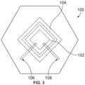
- FIG. 3 illustrates a top view of the antenna element 100 showing an example orientation of the feed lines 106 and 108, according to some of the disclosed implementations.
- the example in FIG. 3 shows a top view of the antenna element 100 with the hybrid radiator comprising the square ring slot 102, the square ring patch 104, and the feed lines 106 and 108.
- a 90-degree sequential rotation may be used to improve array far-field cross-polar performance; though, for single or dual-linear polarization, 90-degree sequential rotation is not used.
- FIG. 4 illustrates a top view of an antenna array 400 with a triangular-array lattice of multiple antenna elements 100a-n, according to some of the disclosed implementations.
- the hexagonal boundaries of antenna elements 100a-n are not visible as there are no dividing walls between the antenna elements 100a-n in the depicted example.
- a triangular lattice is used to form the antenna array 400 to reduce cost compared to a rectangular or square lattice. Eliminating these dividing walls reduces manufacturing cost substantially.
- all antenna elements 100a-n are parallel-fed in phase by a power distribution network on a single layer.
- additional layers are used to house a growing parallel-feed distribution network.
- a series feed may also be used without additional layers but at the expense of reduced bandwidth.
- a hybrid parallel- and series-feed scheme may be used to reach a compromise between lower cost and larger bandwidth.
- the feed lines 106a-n and 108a-n provide two orthogonal polarizations that are each fed independently.
- one-dimensional (ID) antenna beam scanning (left-to-right or right-to-left) may be achieved.
- a 1D antenna beam scanning is sufficient if ultra-low cost is a priority and two-dimensional (2D) scanning is not required.
- a 2D scan may require every element (rather than successive columns of elements for 1D) to be fed by a different phase or time delay, resulting in a much higher manufacturing cost.
- FIG. 5 illustrates a block diagram of an antenna system 500 with an antenna array 502 made up of the disclosed antenna elements 100a-n in this disclosure.
- the antenna system 500 includes a power supply 504, a controller 506, and the antenna array 502.
- the antenna array 502 is a phased array antenna ("PAA") that includes a plurality of the antenna elements 100a-n that operate either transmit and/or receive modules. More specifically, the antenna array 502 may the previously discussed antenna array 400 that uses hexagonal-shaped antenna elements 100, the antenna array 400 that uses a triangular lattice, a combination thereof, or an alternatively shaped antenna array that uses the disclosed square ring slot 102 and square ring patch 104 as an RF transmitter/receiver.
- PAA phased array antenna
- the antenna elements 100a-n of the antenna array 502 include corresponding radiation elements that in combination are capable of transmitting and/or receiving RF signals.
- the antenna elements 100a-n may be configured to operate within a K-band frequency range (e.g., about 20 GHz to 40 GHz for NATO K-band and 18 GHz to 26.5 GHz for IEEE K-band).
- the power supply 504 is a device, component, and/or module that provides power to the controller 506 in the antenna system 500.
- the controller 506 is a device, component, and/or module that controls the operation of the antenna array 502.
- the controller 506 may be a processor, microprocessor, microcontroller, digital signal processor ("DSP"), or other type of device that may either be programmed in hardware and/or software.
- DSP digital signal processor
- the controller 506 controls the electrical feed supplies provided to the antenna array 502, including, without limitation calibrating particular polarization, voltage, frequency, and the like of the electrical feeds. Only one line is shown between the controller 506 and the antenna array 502 for the sake of clarity, but in reality, several electrical connections and supply lines may connect the controller 506 to the antenna array 502.
- the controller 506 supplies the particular electrical feeds to the various antenna elements 100a-n in order to create numerous RF signals that combine, either constructively or destructively, to form a desired cumulative RF signal for transmission.
- RF signals emitted from each antenna element 100a-n in the antenna array 502 may be in phase so as to constructively produce intense radiation or out of phase to destructively create a particular RF signal.
- Direction may be controlled by setting the phase shift between the signals sent to different antenna elements 100a-n.
- the phase shift may be controlled by the controller 506 placing an appropriate phase delay or a slight time delay between signals sent to successive antenna elements 100a-n in the array.
- One antenna system 500 may be in signal communication with another antenna system 500, where signal communication refers to any type of communication and/or connection between the circuits, components, modules, and/or devices that allows a circuit, component, module, and/or device to pass and/or receive signals and/or information from another circuit, component, module, and/or device.
- the communication and/or connection may be along any signal path between the circuits, components, modules, and/or devices that allows signals and/or information to pass from one circuit, component, module, and/or device to another and includes wireless or wired signal paths.
- the signal paths may be physical, such as, for example, conductive wires, electromagnetic wave guides, cables, attached and/or electromagnetic or mechanically coupled terminals, semiconductive or dielectric materials or devices, or other similar physical connections or couplings. Additionally, signal paths may be non-physical such as free-space (in the case of electromagnetic propagation) or information paths through digital components where communication information is passed from one circuit, component, module, and/or device to another in varying digital formats without passing through a
- This antenna system 500 provides a means to send (or receive) RF signals to (or from) airborne or mobile vehicles with an agile electronically scanning antenna array beam without mechanical moving parts.
- the antenna system 500 may be used in communications systems and other applications, including, without limitation, for radar/sensor, electronic warfare, military applications, mobile communications, and the like.
- the antenna system 500 provides a high-performance, light-weight, low-profile and affordable solution to meet challenging and evolving mission requirements.
- FIG. 6 illustrates a perspective view of an aircraft 600 having an antenna array 502 according to various implementations of the present disclosure.
- the aircraft 600 includes a wing 602 and a wing 604 attached to a body 606.
- the aircraft 600 also includes an engine 608 attached to the wing 602 and an engine 610 attached to the wing 604.
- the body 606 has a tail section 612 with a horizontal stabilizer 614, a horizontal stabilizer 616, and a vertical stabilizer 618 attached to the tail section 612 of the body 606.
- the body 606 in some examples has a composite skin 620.
- the previously discussed antenna system 500 which includes the disclosed antenna elements 100 in an antenna array 502 or just the antenna elements 100 individually, may be included onto or in the aircraft 600. This is shown in FIG. 6 with a dotted box.
- the antenna system 500 may be positioned inside or outside of the aircraft 600.
- the illustration of the aircraft 600 is not meant to imply physical or architectural limitations to the manner in which an illustrative configuration may be implemented.
- the aircraft 600 is a commercial aircraft, the aircraft 600 can be a military aircraft, a rotorcraft, a helicopter, an unmanned aerial vehicle, or any other suitable aircraft.
- Other vehicles are possible as well, such as, for example but without limitation, an automobile, a motorcycle, a bus, a boat, a train, or the like.
- various examples facilitate induction welding of parts by improving the heating of (e.g., more uniformly heat) the weld interface between the parts from a single side of the parts.
- the present disclosure can be implemented using different manufacturing environments. For example, some or all aspects of the present disclosure can be implemented at least in the material procurement and component and assembly manufacturing, as described herein.
- the operations illustrated in the figures may be implemented as software instructions encoded on a computer readable medium, in hardware programmed or designed to perform the operations, or both.
- aspects of the disclosure may be implemented as an ASIC, SoC, or other circuitry including a plurality of interconnected, electrically conductive elements.
Landscapes
- Physics & Mathematics (AREA)
- Engineering & Computer Science (AREA)
- Electromagnetism (AREA)
- Manufacturing & Machinery (AREA)
- Astronomy & Astrophysics (AREA)
- Aviation & Aerospace Engineering (AREA)
- General Physics & Mathematics (AREA)
- Remote Sensing (AREA)
- Variable-Direction Aerials And Aerial Arrays (AREA)
- Waveguide Aerials (AREA)
Abstract
Description
- A phased array antenna ("PAA") is a type of antenna that includes a plurality of sub-antennas (generally known as antenna elements, array elements, or radiating elements of the combined antenna) in which the relative amplitudes and phases of the respective signals feeding the array elements may be varied in a way that the effect on the total radiation pattern of the PAA is reinforced in desired directions and suppressed in undesired directions. In other words, a beam may be generated that may be pointed in or steered into different directions. Beam pointing in a transmit or receive PAA is achieved by controlling the amplitude and phase of the transmitted or received signal from each antenna element in the PAA.
- The individual radiated signals are combined to form the constructive and destructive interference patterns produced by the PAA that result in one or more antenna beams. The PAA may then be used to point the beam, or beams, rapidly in azimuth and elevation.
- The disclosed examples are described in detail below with reference to the accompanying drawing figures listed below. The following summary is provided to illustrate examples or implementations disclosed herein. It is not meant, however, to limit all examples to any particular configuration or sequence of operations.
- The disclosed examples and implementations are directed to antenna elements that may be positioned together to form an antenna array (or PAA), which may be affixed or incorporated in curved or conformal structures (e.g., aircraft bodies). The disclosed antenna elements use a number of stacked dielectric layers, at least two of which are separated by a low-dielectric foam layer, such as a core or low-dielectric foam or honeycomb material with low average dielectric constant structure. A horizontal top dielectric layer supports a microstrip square ring patch radiator and also serves as an environmental shield against corrosion. A square ring patch cutout hole reduces the resonance frequency of the patch and allows a smaller outside diameter which is desirable for mutual coupling reduction and avoidance of over-emphasis of broadside antenna gain. A lower section includes two layers of dielectric substrates to support a square ring slot and feed lines (e.g., single line providing single linear polarization or dual feed lines providing dual linear polarization) for providing RF power or carrying away received RF signals. The feed lines excite orthogonal resonant modes in the square ring slot, which, in turn excite orthogonal resonant modes in the square ring patch above. The square ring slot and square ring patch work together to provide a wider impedance bandwidth than either one alone could provide. The antenna elements may operate in transmit or receive RF modes.
- Other technical features may be readily apparent to one skilled in the art from the following figures, descriptions, and claims.
- For a more complete understanding of the present disclosure and its advantages, reference is now made to the following description taken in conjunction with the accompanying drawings, in which like reference numerals represent like parts:
-
FIG. 1 illustrates a perspective view of an antenna element with a square radiator, according to some of the disclosed implementations. -
FIG. 2 illustrates a cut-out side view of an antenna element with a square radiator, according to some of the disclosed implementations; -
FIG. 3 illustrates a top view of the antenna element showing an example orientation of antenna feed lines, according to some of the disclosed implementations; -
FIG. 4 illustrates a top view of an antenna array with a triangular-array lattice of multiple antenna elements, according to some of the disclosed implementations; -
FIG. 5 illustrates a block diagram of an antenna system with an antenna array made up of the disclosed antenna elements in this disclosure; and -
FIG. 6 illustrates a perspective view of an aircraft having one or more array antennas made up of the disclosed antenna elements in this disclosure. - Corresponding reference characters indicate corresponding parts throughout the accompanying drawings.
- The various examples will be described in detail with reference to the accompanying drawings. Wherever possible, the same reference numbers will be used throughout the drawings to refer to the same or like parts. References made throughout this disclosure relating to specific examples and implementations are provided solely for illustrative purposes but, unless indicated to the contrary, are not meant to limit all implementations.
- A phased array antenna (PAA) includes multiple emitters and is used for beamforming in high-frequency RF applications, such as in radar, 5G, or myriad other application. The number of emitters in a PAA can range from a few into the thousands. The goal in using a PAA is to control the direction of an emitted beam by exploiting constructive interference between two or more radiated signals. This is known as "beamforming" in the antenna community.
- More specifically, a PAA enables beamforming by adjusting the phase difference between the driving signal sent to each emitter in the array. This allows the radiation pattern to be controlled and directed to a target without requiring any physical movement of the antenna. This means that beamforming along a specific direction is an interference effect between quasi-omnidirectional emitters (e.g., dipole antennas).
- The disclosed implementations and examples provide an ultra-low-cost unit cell antenna element with unique feed structure for an electronically scanning array. The antenna element includes circuit board-like sections and low-dielectric spacers, such as a foam or core structure. A top section of the antenna element includes a layer of dielectric substrate to support a microstrip ring patch radiator. A bottom section has one layer of dielectric substrates to support a ring slot and dual feed lines. The disclosed antenna elements provide high-quality antenna performance over wide frequency bandwidth and up to +/-45 deg 1D scan range (from antenna normal) as well as dual-linear polarizations and circular polarization.
- The disclosed antenna elements are able to send or receive RF signals to and from vehicles and aircraft with an agile electronically-scanning antenna array beam without mechanical moving parts. The antenna elements may be assembled into an antenna array that may be used in a host of applications, such as, for example but without limitation, for radar, sensor, or other applications. The antenna elements provide a high-performance, light-weight, low-profile, and ultra-low-cost solution to meet challenging and evolving mission requirements. Moreover, the disclosed antenna elements are used in the fabrication of integrated and structurally-integrated antennas, specifically in composite sandwich panels due to the minimal use of through-depth vias and connections.
- Conventional antennas use relatively bulky waveguide-based antenna radiators to form the aperture section of an electronically scanning antenna array system. Such systems are mechanically complex and expensive to manufacture and are not expected to meet customer demands in the future. Modern solutions require complex multiple-layer boards with many through-thickness connections. These multi-layer designs do not lend themselves to low-cost manufacturing or to integrated composite manufacturing.
-
Figure 1 shows an embodiment of the invention using circuit board-like sections to form a unit cell in a periodic antenna array environment. The top section has one layer of dielectric substrate or low-cost circuit board to support a microstrip square-ring patch radiator on the underside and also serves as an environmental shield against corrosion. The square-ring patch cutout hole reduces the resonance frequency of the patch and allows a smaller outside diameter which is desirable for mutual coupling reduction and avoidance of over-emphasis of broadside antenna gain. While a square shape is illustrated here other geometries such as circular may be used. - The bottom section has one layer of dielectric substrate or circuit board to support a square-ring slot on the top side and dual feed lines on the bottom side. The feed lines excite orthogonal resonant modes in the square-ring slot which in turn excite orthogonal resonant modes in the square-ring patch above. The square-ring slot and patch work together to provide a wider impedance bandwidth than either one alone could provide. This hybrid radiator is designed to work in both transmit and receive modes. A metallic ground plane is provided by a dielectric substrate or circuit board at the bottom of the structure to redirect backward radiation to the forward direction. This back board also provides mechanical symmetry and support.
-
FIG. 1 illustrates a perspective view of anantenna element 100 with a square radiator, according to some of the disclosed implementations. The square radiator is made up of asquare ring slot 102 and asquare ring patch 104 that operate to transmit or receive RF signals. Thesquare ring slot 102 and thesquare ring patch 104 collectively create a "square radiator" for transmitting and/or receiving RF signals. In some implementations, thesquare ring patch 104 has a larger perimeter than thesquare ring slot 102. - The
antenna element 100 also includes circuit board-like sections to form a unit cell in a periodic antenna array environment. Three dielectric layers are stacked on top of each other and separated: atop dielectric layer 110,middle dielectric layer 112, andbottom dielectric layer 114. Two foam layers,upper foam layer 116 andlower foam layer 118, separate the dielectric layers 110-114 from each other. These foam layers 116-118 may be any kind of a dielectric material with low average dielectric constant, such as, for example but without limitation, a foam layer. As shown, the dielectric layers 110-114 and foam layers 116-118 are the same hexagonal shape, providing mechanical symmetry and support. Other shapes are fully contemplated, e.g., circular, rectangular, square, octagonal, etc. - To aid the reader, an
upper section 120 is depicted as well as alower section 122. Also, the various components are discussed in relation to directions that assume the "top" and "upper" portions are located at "A" and the "bottom" and "lower" portions are located at "B." - The
upper section 120 includes thesquare ring patch 104, thetop dielectric layer 110, theupper foam layer 116. Thelower section 122 includes thesquare ring slot 102, themiddle dielectric layer 112, and thelower foam layer 118. Themiddle dielectric layer 112 supports thesquare ring slot 102 on the top side and thefeed lines - While
dual feed lines dual feed lines - The
lower section 122 includes two layers of dielectric substrates, themiddle dielectric layer 112 and thebottom dielectric layer 114, that collectively support thesquare ring slot 102,dual feed lines square ring slot 102, which, in turn excites orthogonal resonant modes in thesquare ring patch 104 above for RF signaling. When transmitting RF signals, theelectrical feed lines square ring slot 102 that, then, generates the desired RF signal in thesquare ring patch 104. When receiving RF signals, theelectrical feed lines square ring slot 102 from thesquare ring patch 104 receiving an RF signal. - The
square ring patch 104 is metallic or otherwise electrically conductive. Electricity is supplied to theantenna element 100 through thefeed lines square ring slot 102 and thesquare ring patch 104 to operate as a radiating element for generating specific RF signals. As can be seen, thesquare ring patch 104 is positioned vertically above thesquare ring slot 102, at least in some implementations. - In operation, the dual
electrical feed lines -
FIG. 2 illustrates a cut-out side view of theantenna element 100 discussed above inFIG. 1 , according to some of the disclosed implementations. Thetop dielectric layer 110 and themiddle dielectric layer 112 are separated by theupper foam layer 116. Themiddle dielectric layer 112 and thebottom dielectric layer 114 are separated by thelower foam layer 118, which extends down to thebottom dielectric layer 114. Thesquare ring patch 104 is positioned above theupper foam layer 116 and below thetop dielectric layer 110. Reference direction A and B are illustrated to show the corresponding top and bottom of theantenna element 100, respectively. - The
square ring slot 102 is a thin metal (or other conductive material) layer that is positioned above themiddle dielectric layer 112 facing toward the top of theantenna element 100, below theupper foam layer 116. The feed lines 106 and 108 are also metal (or other conductive material) positioned on the bottom side of themiddle dielectric layer 112 facing toward bottom of theantenna element 100, above thelower foam layer 118. - The
upper foam layer 116 operates as a spacer between thesquare ring slot 102 and thesquare ring patch 104, providing a low average dielectric constant close to air to maximize scan impedance bandwidth and suppress unwanted dielectric modes. Thelower foam layer 118 operates as a spacer between thesquare ring slot 102 and thebottom dielectric layer 114, which operates as a back plane. Similar to theupper foam layer 116, thelower foam layer 118 provides a low dielectric constant close to air to maximize scan impedance bandwidth and suppress unwanted dielectric modes. -
FIG. 3 illustrates a top view of theantenna element 100 showing an example orientation of thefeed lines FIG. 3 shows a top view of theantenna element 100 with the hybrid radiator comprising thesquare ring slot 102, thesquare ring patch 104, and thefeed lines -
FIG. 4 illustrates a top view of anantenna array 400 with a triangular-array lattice ofmultiple antenna elements 100a-n, according to some of the disclosed implementations. The hexagonal boundaries ofantenna elements 100a-n are not visible as there are no dividing walls between theantenna elements 100a-n in the depicted example. A triangular lattice is used to form theantenna array 400 to reduce cost compared to a rectangular or square lattice. Eliminating these dividing walls reduces manufacturing cost substantially. For each column of theantenna array 400, allantenna elements 100a-n are parallel-fed in phase by a power distribution network on a single layer. For a larger antenna array, additional layers are used to house a growing parallel-feed distribution network. Alternatively, a series feed may also be used without additional layers but at the expense of reduced bandwidth. Further still, a hybrid parallel- and series-feed scheme may be used to reach a compromise between lower cost and larger bandwidth. - In the shown implementation, the feed lines 106a-n and 108a-n provide two orthogonal polarizations that are each fed independently. By applying a time-delay or phase gradient across the different columns of the array, one-dimensional (ID) antenna beam scanning (left-to-right or right-to-left) may be achieved. For some radar or sensor applications, a 1D antenna beam scanning is sufficient if ultra-low cost is a priority and two-dimensional (2D) scanning is not required. A 2D scan may require every element (rather than successive columns of elements for 1D) to be fed by a different phase or time delay, resulting in a much higher manufacturing cost.
-
FIG. 5 illustrates a block diagram of anantenna system 500 with anantenna array 502 made up of the disclosedantenna elements 100a-n in this disclosure. In this example, theantenna system 500 includes apower supply 504, acontroller 506, and theantenna array 502. In this example, theantenna array 502 is a phased array antenna ("PAA") that includes a plurality of theantenna elements 100a-n that operate either transmit and/or receive modules. More specifically, theantenna array 502 may the previously discussedantenna array 400 that uses hexagonal-shapedantenna elements 100, theantenna array 400 that uses a triangular lattice, a combination thereof, or an alternatively shaped antenna array that uses the disclosedsquare ring slot 102 andsquare ring patch 104 as an RF transmitter/receiver. Thus, theantenna elements 100a-n of theantenna array 502 include corresponding radiation elements that in combination are capable of transmitting and/or receiving RF signals. For example, theantenna elements 100a-n may be configured to operate within a K-band frequency range (e.g., about 20 GHz to 40 GHz for NATO K-band and 18 GHz to 26.5 GHz for IEEE K-band). - The
power supply 504 is a device, component, and/or module that provides power to thecontroller 506 in theantenna system 500. Thecontroller 506 is a device, component, and/or module that controls the operation of theantenna array 502. Thecontroller 506 may be a processor, microprocessor, microcontroller, digital signal processor ("DSP"), or other type of device that may either be programmed in hardware and/or software. Thecontroller 506 controls the electrical feed supplies provided to theantenna array 502, including, without limitation calibrating particular polarization, voltage, frequency, and the like of the electrical feeds. Only one line is shown between thecontroller 506 and theantenna array 502 for the sake of clarity, but in reality, several electrical connections and supply lines may connect thecontroller 506 to theantenna array 502. - In some implementations, the
controller 506 supplies the particular electrical feeds to thevarious antenna elements 100a-n in order to create numerous RF signals that combine, either constructively or destructively, to form a desired cumulative RF signal for transmission. RF signals emitted from eachantenna element 100a-n in theantenna array 502 may be in phase so as to constructively produce intense radiation or out of phase to destructively create a particular RF signal. Direction may be controlled by setting the phase shift between the signals sent todifferent antenna elements 100a-n. The phase shift may be controlled by thecontroller 506 placing an appropriate phase delay or a slight time delay between signals sent tosuccessive antenna elements 100a-n in the array. - One
antenna system 500 may be in signal communication with anotherantenna system 500, where signal communication refers to any type of communication and/or connection between the circuits, components, modules, and/or devices that allows a circuit, component, module, and/or device to pass and/or receive signals and/or information from another circuit, component, module, and/or device. The communication and/or connection may be along any signal path between the circuits, components, modules, and/or devices that allows signals and/or information to pass from one circuit, component, module, and/or device to another and includes wireless or wired signal paths. The signal paths may be physical, such as, for example, conductive wires, electromagnetic wave guides, cables, attached and/or electromagnetic or mechanically coupled terminals, semiconductive or dielectric materials or devices, or other similar physical connections or couplings. Additionally, signal paths may be non-physical such as free-space (in the case of electromagnetic propagation) or information paths through digital components where communication information is passed from one circuit, component, module, and/or device to another in varying digital formats without passing through a direct electromagnetic connection. - This
antenna system 500 provides a means to send (or receive) RF signals to (or from) airborne or mobile vehicles with an agile electronically scanning antenna array beam without mechanical moving parts. Theantenna system 500 may be used in communications systems and other applications, including, without limitation, for radar/sensor, electronic warfare, military applications, mobile communications, and the like. Theantenna system 500 provides a high-performance, light-weight, low-profile and affordable solution to meet challenging and evolving mission requirements. -
FIG. 6 illustrates a perspective view of anaircraft 600 having anantenna array 502 according to various implementations of the present disclosure. Theaircraft 600 includes awing 602 and awing 604 attached to abody 606. Theaircraft 600 also includes anengine 608 attached to thewing 602 and anengine 610 attached to thewing 604. Thebody 606 has atail section 612 with ahorizontal stabilizer 614, ahorizontal stabilizer 616, and avertical stabilizer 618 attached to thetail section 612 of thebody 606. Thebody 606 in some examples has acomposite skin 620. - In some examples, the previously discussed
antenna system 500, which includes the disclosedantenna elements 100 in anantenna array 502 or just theantenna elements 100 individually, may be included onto or in theaircraft 600. This is shown inFIG. 6 with a dotted box. Theantenna system 500 may be positioned inside or outside of theaircraft 600. - The illustration of the
aircraft 600 is not meant to imply physical or architectural limitations to the manner in which an illustrative configuration may be implemented. For example, although theaircraft 600 is a commercial aircraft, theaircraft 600 can be a military aircraft, a rotorcraft, a helicopter, an unmanned aerial vehicle, or any other suitable aircraft. Other vehicles are possible as well, such as, for example but without limitation, an automobile, a motorcycle, a bus, a boat, a train, or the like. - Thus, various examples facilitate induction welding of parts by improving the heating of (e.g., more uniformly heat) the weld interface between the parts from a single side of the parts. The present disclosure, including the examples described herein, can be implemented using different manufacturing environments. For example, some or all aspects of the present disclosure can be implemented at least in the material procurement and component and assembly manufacturing, as described herein.
- The following clauses describe further aspects of the present disclosure. In some implementations, the clauses described below can be further combined in any sub-combination without departing from the scope of the present disclosure.
-
- A1: An antenna element for generating a radio frequency (RF) signal, comprising:
- a plurality of dielectric layers comprising a top dielectric layer, a middle dielectric layer, and a bottom dielectric layer;
- a square ring patch positioned in the top dielectric layer;
- a square ring slot;
- a plurality of foam layers between the plurality of dielectric layers, wherein an upper foam layer separates the square ring patch from the square ring slot; and
- electrical feed lines supplying electrical power to generate electrical resonance in square the square ring slot for producing the RF signal in the square ring patch.
- A2: The antenna element of claim A1, wherein the plurality of dielectric layers comprise one or more printed circuit boards.
- A3: The antenna element of claims A1 or A2, wherein the square ring patch has a larger perimeter than the square ring slot.
- A4: The antenna element of any of claims A1-A3, wherein the plurality of foam layers are made of a low-dielectric foam or honeycomb material with low average dielectric constant.
- A5: The antenna element of any of claims A1-A4, wherein the plurality of dielectric layers comprise a top dielectric layer, a middle dielectric layer, and a bottom dielectric layer.
- A6: The antenna element of any of claims A1-A5, wherein the upper foam layer separates the top dielectric layer from the middle dielectric layer, and wherein the square ring patch is positioned between the top dielectric layer and the upper foam layer.
- A7: The antenna element of any of claims A1-A6, wherein the electrical feed lines are positioned at or about 90-degrees of rotation from each other.
-
- B1: An antenna element for generating or receiving radio frequency (RF) signal, comprising:
- a plurality of dielectric layers comprising a top dielectric layer, a middle dielectric layer, and a bottom dielectric layer;
- a square ring patch positioned in the top dielectric layer;
- a square ring slot;
- a plurality of foam layers between the plurality of dielectric layers, wherein an upper foam layer separates the square ring patch from the square ring slot; and
- electrical feed lines receiving electrical power generated from electrical resonance received by the square ring patch and induced in the square ring slot.
- B2: The antenna element of claim B1, wherein the plurality of dielectric layers comprise one or more printed circuit boards.
- B3: The antenna element of claims B 1 or B2, wherein the square ring patch has a larger perimeter than the square ring slot.
- B4: The antenna element of any of claims B1-B3, wherein the plurality of foam layers are made of a low-dielectric foam or honeycomb material with low average dielectric constant.
- B5: The antenna element of any of claims B1-B4, wherein the plurality of dielectric layers comprise a top dielectric layer, a middle dielectric layer, and a bottom dielectric layer.
- B6: The antenna element of any of claims B1-B5, wherein the upper foam layer separates the top dielectric layer from the middle dielectric layer, and wherein the square ring patch is positioned between the top dielectric layer and the upper foam layer.
- B7: The antenna element of any of claims B1-B6, wherein the electrical feed lines are positioned at or about 90-degrees of rotation from each other.
- B8: The antenna element of any of claims B1-B7, wherein the plurality of dielectric layers are hexagonally shaped (100)
- B9. The antenna element of any of claims B1-B8, wherein the antenna element is disposed on an airplane (700).
-
- C1: An antenna array for communicating a radio frequency (RF) signal, comprising:
a plurality of antenna elements positioned in an antenna array, each antenna cell comprising:- a plurality of dielectric layers comprising a top dielectric layer, a middle dielectric layer, and a bottom dielectric layer;
- a square ring patch positioned in the top dielectric layer;
- a square ring slot;
- a plurality of foam layers between the plurality of dielectric layers,
electrical feed lines supplying electrical power to generate electrical resonance in the square ring slot for producing the RF signal in the square ring patch. - C2: The antenna array of claim C1, wherein the plurality of dielectric layers are hexagonally shaped.
- C3: The antenna array of claim C1, wherein the plurality of antenna elements are arranged in a triangular-array lattice with multiple antenna elements.
- C4: The antenna array of claim C1, wherein the antenna array is disposed on an airplane.
-
- D1: An antenna array for communicating a radio frequency (RF) signal, comprising:
a plurality of antenna elements positioned in an array, each antenna cell comprising:- a plurality of dielectric layers comprising a top dielectric layer, a middle dielectric layer, and a bottom dielectric layer;
- a ring patch positioned in the top dielectric layer for receiving the RF signal;
- a foam layer between the top dielectric layer and the middle dielectric layer;
- a ring slot position between the foam layer and the middle dielectric layer, wherein the square ring slot being positioned to electromagnetically receive the RF signal from the square ring patch; and
- electrical feed lines positioned to output the RF signal received by the square ring slot as an output.
- D2: The antenna array of claim D1, wherein the plurality of dielectric layers are hexagonally shaped.
- D3: The antenna array of claim D1, wherein the plurality of antenna elements are arranged in a triangular-array lattice with multiple antenna elements.
- D4: The antenna array of claim D1, wherein the antenna array is disposed on an airplane.
- Although the subject matter has been described in language specific to structural features and/or methodological acts, it is to be understood that the subject matter defined in the appended claims is not necessarily limited to the specific features or acts described above. Rather, the specific features and acts described above are disclosed as example forms of implementing the claims.
- It will be understood that the benefits and advantages described above may relate to one implementation or may relate to several implementations. The implementations are not limited to those that solve any or all of the stated problems or those that have any or all of the stated benefits and advantages. It will further be understood that reference to 'an' item refers to one or more of those items.
- The term "comprising" is used in this disclosure to mean including the feature(s) or act(s) followed thereafter, without excluding the presence of one or more additional features or acts.
- In some examples, the operations illustrated in the figures may be implemented as software instructions encoded on a computer readable medium, in hardware programmed or designed to perform the operations, or both. For example, aspects of the disclosure may be implemented as an ASIC, SoC, or other circuitry including a plurality of interconnected, electrically conductive elements.
- The order of execution or performance of the operations in examples of the disclosure illustrated and described herein is not essential, unless otherwise specified. That is, the operations may be performed in any order, unless otherwise specified, and examples of the disclosure may include additional or fewer operations than those disclosed herein. For example, it is contemplated that executing or performing a particular operation before, contemporaneously with, or after another operation is within the scope of aspects of the disclosure.
- When introducing elements of aspects of the disclosure or the examples thereof, the articles "a," "an," "the," and "said" are intended to mean that there are one or more of the elements. The terms "comprising," "including," and "having" are intended to be inclusive and mean that there may be additional elements other than the listed elements. The term "exemplary" is intended to mean "an example of." The phrase "one or more of the following: A, B, and C" means "at least one of A and/or at least one of B and/or at least one of C."
- Having described aspects of the disclosure in detail, it will be apparent that modifications and variations are possible without departing from the scope of aspects of the disclosure as defined in the appended claims. As various changes could be made in the above constructions, products, and methods without departing from the scope of aspects of the disclosure, it is intended that all matter contained in the above description and shown in the accompanying drawings shall be interpreted as illustrative and not in a limiting sense.
- It is to be understood that the above description is intended to be illustrative, and not restrictive. As an illustration, the above-described implementations (and/or aspects thereof) are usable in combination with each other. In addition, many modifications are practicable to adapt a particular situation or material to the teachings of the various implementations of the disclosure without departing from their scope. While the dimensions and types of materials described herein are intended to define the parameters of the various implementations of the disclosure, the implementations are by no means limiting and are exemplary implementations. Many other implementations will be apparent to those of ordinary skill in the art upon reviewing the above description. The scope of the various implementations of the disclosure should, therefore, be determined with reference to the appended claims, along with the full scope of equivalents to which such claims are entitled. In the appended claims, the terms "including" and "in which" are used as the plain-English equivalents of the respective terms "comprising" and "wherein." Further, the limitations of the following claims are not written in means-plus-function format and are not intended to be interpreted based on 35 U.S.C. § 112(f), unless and until such claim limitations expressly use the phrase "means for" followed by a statement of function void of further structure.
- This written description uses examples to disclose the various implementations of the disclosure, including the best mode, and also to enable any person of ordinary skill in the art to practice the various implementations of the disclosure, including making and using any devices or systems and performing any incorporated methods. The patentable scope of the various implementations of the disclosure is defined by the claims, and includes other examples that occur to those persons of ordinary skill in the art. Such other examples are intended to be within the scope of the claims if the examples have structural elements that do not differ from the literal language of the claims, or if the examples include equivalent structural elements with insubstantial differences from the literal language of the claims.
- Although the present disclosure has been described with reference to various implementations, various changes and modifications can be made without departing from the scope of the present disclosure.
Claims (15)
- An antenna element (100) for generating a radio frequency ,RF, signal, comprising:a plurality of dielectric layers comprising a top dielectric layer (110), a middle dielectric layer (112), and a bottom dielectric layer (114);a square ring patch (104) positioned in the top dielectric layer (110);a square ring slot (102);a plurality of foam layers (116, 118) between the plurality of dielectric layers (110, 112, 114), wherein an upper foam layer (116) separates the square ring patch (104) from the square ring slot (102); andelectrical feed lines (106, 108) supplying electrical power to generate electrical resonance in the square ring slot (102) for producing the RF signal in the square ring patch (104).
- The antenna element (100) of claim 1, wherein the plurality of dielectric layers (110, 112, 114) comprise one or more printed circuit boards.
- The antenna element (100) of claims 1 or 2, wherein the square ring patch (104) has a larger perimeter than the square ring slot (102).
- The antenna element (100) of any of claims 1-3, wherein the plurality of foam layers (116, 118) are made of a honeycomb foam low-dielectric foam or honeycomb material with low average dielectric constant.
- The antenna element (100) of any of claims 1-4, wherein the upper foam layer (116) separates the top dielectric layer (110) from the middle dielectric layer (112), and wherein the square ring patch (104) is positioned between the top dielectric layer (110) and the upper foam layer (116).
- The antenna element (100) of any of claims 1-5, wherein the electrical feed lines (106, 108) are positioned at or about 90-degrees of rotation from each other.
- An antenna element (100) for generating or receiving radio frequency (RF) signal, comprising:a plurality of dielectric layers comprising a top dielectric layer (110), a middle dielectric layer (112), and a bottom dielectric layer (114);a square ring patch (104) positioned in the top dielectric layer (110);a square ring slot (102);a plurality of foam layers (116, 118) between the plurality of dielectric layers (110, 112, 114), wherein an upper foam layer (116) separates the square ring patch (104) from the square ring slot (102); andelectrical feed lines (106, 108) receiving electrical power generated from electrical resonance received by the square ring patch (104) and induced in the square ring slot (102).
- The antenna element (100) of claim 7, wherein the plurality of dielectric layers (110, 112, 114) comprise one or more printed circuit boards.
- The antenna element (100) of claims 7 or 8, wherein the square ring patch (104) has a larger perimeter than the square ring slot (102).
- The antenna element (100) of claim 7-9, wherein the plurality of foam layers (116, 118) are made of a low-dielectric foam or honeycomb material with low average dielectric constant.
- The antenna element (100) of any of claims 7-10, wherein the upper foam layer (116) separates the top dielectric layer (110) from the middle dielectric layer (112), and wherein the square ring patch (104) is positioned between the top dielectric layer (110) and the upper foam layer (116).
- The antenna element (100) of any of claims 7-11, wherein the electrical feed lines (106, 108) are positioned at or about 90-degrees of rotation from each other.
- The antenna element (100) of any of claims 7-12, wherein the plurality of dielectric layers (110, 112, 114) are hexagonally shaped.
- The antenna element (100) of any of claims 7-13, wherein the antenna element is disposable on an airplane (600).
- An antenna system (500) comprising an antenna array (502) made up of antenna elements (100a-n) according to any one of the preceding claims, a power supply (504) and a controller (506).
Applications Claiming Priority (2)
| Application Number | Priority Date | Filing Date | Title |
|---|---|---|---|
| US202163251573P | 2021-10-01 | 2021-10-01 | |
| US17/588,178 US12266862B2 (en) | 2021-10-01 | 2022-01-28 | Ultra-low-cost 1D-scanning antenna array |
Publications (1)
| Publication Number | Publication Date |
|---|---|
| EP4160816A1 true EP4160816A1 (en) | 2023-04-05 |
Family
ID=83447731
Family Applications (1)
| Application Number | Title | Priority Date | Filing Date |
|---|---|---|---|
| EP22196914.0A Pending EP4160816A1 (en) | 2021-10-01 | 2022-09-21 | Ultra-low-cost 1d-scanning antenna array |
Country Status (3)
| Country | Link |
|---|---|
| US (2) | US12266862B2 (en) |
| EP (1) | EP4160816A1 (en) |
| CN (1) | CN115939741A (en) |
Families Citing this family (4)
| Publication number | Priority date | Publication date | Assignee | Title |
|---|---|---|---|---|
| US12456808B2 (en) | 2021-10-01 | 2025-10-28 | The Boeing Company | High isolation ring slot patch radiator for phased array antennas |
| US12562499B2 (en) * | 2022-12-15 | 2026-02-24 | Peraso Technologies Inc. | Dual-band phased array antenna assembly |
| EP4576420A1 (en) * | 2023-12-18 | 2025-06-25 | The Boeing Company | High isolation ring slot patch radiator for phased array antennas |
| US20260094975A1 (en) * | 2024-10-01 | 2026-04-02 | The United States Of America, As Represented By The Secretary Of The Navy | Omnidirectional Conformal Antenna Power Pattern and Method Thereof |
Citations (2)
| Publication number | Priority date | Publication date | Assignee | Title |
|---|---|---|---|---|
| US5055852A (en) * | 1989-06-20 | 1991-10-08 | Alcatel Espace | Diplexing radiating element |
| US20150084814A1 (en) * | 2012-03-14 | 2015-03-26 | Israel Aerospace Industries Ltd. | Phased array antenna |
Family Cites Families (13)
| Publication number | Priority date | Publication date | Assignee | Title |
|---|---|---|---|---|
| WO2003034545A1 (en) * | 2001-10-16 | 2003-04-24 | Fractus, S.A. | Multifrequency microstrip patch antenna with parasitic coupled elements |
| JP3420233B2 (en) * | 2001-11-28 | 2003-06-23 | 日本アンテナ株式会社 | Composite antenna |
| GB0305081D0 (en) * | 2003-03-06 | 2003-04-09 | Qinetiq Ltd | Microwave connector, antenna and method of manufacture of same |
| KR100993125B1 (en) * | 2003-03-11 | 2010-11-08 | 엘지이노텍 주식회사 | Circularly Polarized Microstrip Ring Structure Antenna |
| US7486239B1 (en) * | 2007-09-27 | 2009-02-03 | Eswarappa Channabasappa | Multi-polarization planar antenna |
| US8350771B1 (en) * | 2009-06-02 | 2013-01-08 | The United States Of America, As Represented By The Secretary Of The Navy | Dual-band dual-orthogonal-polarization antenna element |
| US8773323B1 (en) * | 2011-03-18 | 2014-07-08 | The Boeing Company | Multi-band antenna element with integral faraday cage for phased arrays |
| US11456534B2 (en) * | 2018-07-12 | 2022-09-27 | The United States Of America As Represented By The Secretary Of The Army | Broadband stacked parasitic geometry for a multi-band and dual polarization antenna |
| JP7107105B2 (en) * | 2018-08-30 | 2022-07-27 | Tdk株式会社 | antenna |
| CN111834731B (en) * | 2019-04-19 | 2022-03-01 | Oppo广东移动通信有限公司 | Antenna module and electronic equipment |
| CN110212300B (en) * | 2019-05-22 | 2021-05-11 | 维沃移动通信有限公司 | An antenna unit and terminal equipment |
| US11322833B2 (en) * | 2019-06-03 | 2022-05-03 | Space Exploration Technologies Corp. | Antenna apparatus having fastener system |
| US11695219B2 (en) * | 2021-05-17 | 2023-07-04 | America as represented by the Secretary of the Army | Broadband stacked patch antenna array |
-
2022
- 2022-01-28 US US17/588,178 patent/US12266862B2/en active Active
- 2022-09-21 EP EP22196914.0A patent/EP4160816A1/en active Pending
- 2022-09-28 CN CN202211189393.6A patent/CN115939741A/en active Pending
-
2025
- 2025-03-27 US US19/092,427 patent/US20250253546A1/en active Pending
Patent Citations (2)
| Publication number | Priority date | Publication date | Assignee | Title |
|---|---|---|---|---|
| US5055852A (en) * | 1989-06-20 | 1991-10-08 | Alcatel Espace | Diplexing radiating element |
| US20150084814A1 (en) * | 2012-03-14 | 2015-03-26 | Israel Aerospace Industries Ltd. | Phased array antenna |
Non-Patent Citations (1)
| Title |
|---|
| THE-NAN CHANG ET AL: "A Circularly Polarized Ring-Antenna Fed by a Serially Coupled Square Slot-Ring", IEEE TRANSACTIONS ON ANTENNAS AND PROPAGATION, IEEE, USA, vol. 60, no. 2, 21 October 2011 (2011-10-21), pages 1132 - 1135, XP011403516, ISSN: 0018-926X, DOI: 10.1109/TAP.2011.2173138 * |
Also Published As
| Publication number | Publication date |
|---|---|
| US12266862B2 (en) | 2025-04-01 |
| US20250253546A1 (en) | 2025-08-07 |
| US20230104894A1 (en) | 2023-04-06 |
| CN115939741A (en) | 2023-04-07 |
Similar Documents
| Publication | Publication Date | Title |
|---|---|---|
| EP4160816A1 (en) | Ultra-low-cost 1d-scanning antenna array | |
| EP3561951B1 (en) | Unit cell antenna for phased arrays | |
| Mahfuz et al. | Review of patch antennas used in drone applications | |
| US10283876B1 (en) | Dual-polarized, planar slot-aperture antenna element | |
| US10978812B2 (en) | Single layer shared aperture dual band antenna | |
| US20250210860A1 (en) | Low cost electronically scanning antenna array architecture | |
| US20260051658A1 (en) | High isolation ring slot patch radiator for phased array antennas | |
| KR101683679B1 (en) | Conformal Patch Type of Array Antenna | |
| US20210083376A1 (en) | Steerable antenna assembly | |
| Reis et al. | General Overview of Antennas for Unmanned Aerial Vehicles: A Review | |
| US11380989B2 (en) | Method to optimally reduce antenna array grating lobes on a conformal surface | |
| US12021305B1 (en) | Conformal antenna system | |
| EP4160819A1 (en) | Ring slot patch radiator unit cell for phased array antennas | |
| EP4228096B1 (en) | Unit cell antenna for phased arrays | |
| US8604985B1 (en) | Dual polarization antenna with high port isolation | |
| Chu et al. | Coding metasurface integrated dual-band antenna for vehicular communications | |
| US11397284B2 (en) | Flexible hybrid electronic sensing system for UAV applications | |
| US11201410B2 (en) | Stripline fed full wavelength slot in half wavelength patch antenna | |
| US11038273B1 (en) | Electronically scanning antenna assembly | |
| EP4576420A1 (en) | High isolation ring slot patch radiator for phased array antennas | |
| CN116073128A (en) | A Wing Conformal End-Fire Phased Array Antenna Based on Pattern Optimization of Array Elements | |
| US12316013B1 (en) | Ultra-broadband current sheet array | |
| Kedar et al. | Parametric Analysis of Unmanned Aerial Vehicle Based Antenna Arrays | |
| Haykir et al. | Compact and Directional Printed Dipole Antenna Pair Conformed on a Conical Surface | |
| Solbach | Aircraft antennas/conformal antennas missile antennas |
Legal Events
| Date | Code | Title | Description |
|---|---|---|---|
| PUAI | Public reference made under article 153(3) epc to a published international application that has entered the european phase |
Free format text: ORIGINAL CODE: 0009012 |
|
| STAA | Information on the status of an ep patent application or granted ep patent |
Free format text: STATUS: THE APPLICATION HAS BEEN PUBLISHED |
|
| AK | Designated contracting states |
Kind code of ref document: A1 Designated state(s): AL AT BE BG CH CY CZ DE DK EE ES FI FR GB GR HR HU IE IS IT LI LT LU LV MC MK MT NL NO PL PT RO RS SE SI SK SM TR |
|
| STAA | Information on the status of an ep patent application or granted ep patent |
Free format text: STATUS: REQUEST FOR EXAMINATION WAS MADE |
|
| 17P | Request for examination filed |
Effective date: 20230904 |
|
| RBV | Designated contracting states (corrected) |
Designated state(s): AL AT BE BG CH CY CZ DE DK EE ES FI FR GB GR HR HU IE IS IT LI LT LU LV MC MK MT NL NO PL PT RO RS SE SI SK SM TR |
|
| GRAP | Despatch of communication of intention to grant a patent |
Free format text: ORIGINAL CODE: EPIDOSNIGR1 |
|
| STAA | Information on the status of an ep patent application or granted ep patent |
Free format text: STATUS: GRANT OF PATENT IS INTENDED |
|
| INTG | Intention to grant announced |
Effective date: 20251112 |
|
| GRAJ | Information related to disapproval of communication of intention to grant by the applicant or resumption of examination proceedings by the epo deleted |
Free format text: ORIGINAL CODE: EPIDOSDIGR1 |
|
| STAA | Information on the status of an ep patent application or granted ep patent |
Free format text: STATUS: REQUEST FOR EXAMINATION WAS MADE |
|
| INTC | Intention to grant announced (deleted) | ||
| GRAP | Despatch of communication of intention to grant a patent |
Free format text: ORIGINAL CODE: EPIDOSNIGR1 |
|
| STAA | Information on the status of an ep patent application or granted ep patent |
Free format text: STATUS: GRANT OF PATENT IS INTENDED |