EP4160698A1 - Upright photovoltaic cell with front contacts - Google Patents
Upright photovoltaic cell with front contacts Download PDFInfo
- Publication number
- EP4160698A1 EP4160698A1 EP22187288.0A EP22187288A EP4160698A1 EP 4160698 A1 EP4160698 A1 EP 4160698A1 EP 22187288 A EP22187288 A EP 22187288A EP 4160698 A1 EP4160698 A1 EP 4160698A1
- Authority
- EP
- European Patent Office
- Prior art keywords
- mesa
- contact
- substrate
- photovoltaic cell
- region
- Prior art date
- Legal status (The legal status is an assumption and is not a legal conclusion. Google has not performed a legal analysis and makes no representation as to the accuracy of the status listed.)
- Pending
Links
- 239000000758 substrate Substances 0.000 claims abstract description 86
- 238000000034 method Methods 0.000 claims abstract description 69
- 239000000463 material Substances 0.000 claims abstract description 63
- 238000000151 deposition Methods 0.000 claims abstract description 24
- 238000005530 etching Methods 0.000 claims abstract description 22
- 239000004065 semiconductor Substances 0.000 claims description 21
- 230000003667 anti-reflective effect Effects 0.000 claims description 11
- 229910052751 metal Inorganic materials 0.000 claims description 10
- 239000002184 metal Substances 0.000 claims description 10
- 238000003486 chemical etching Methods 0.000 claims description 4
- 238000000227 grinding Methods 0.000 claims description 4
- 238000010329 laser etching Methods 0.000 claims description 4
- 230000002153 concerted effect Effects 0.000 claims description 2
- 230000008020 evaporation Effects 0.000 claims description 2
- 238000001704 evaporation Methods 0.000 claims description 2
- 238000005245 sintering Methods 0.000 claims description 2
- 238000004519 manufacturing process Methods 0.000 description 7
- 238000003466 welding Methods 0.000 description 7
- 230000008901 benefit Effects 0.000 description 6
- JBRZTFJDHDCESZ-UHFFFAOYSA-N AsGa Chemical compound [As]#[Ga] JBRZTFJDHDCESZ-UHFFFAOYSA-N 0.000 description 5
- 229910001218 Gallium arsenide Inorganic materials 0.000 description 5
- 239000002800 charge carrier Substances 0.000 description 5
- 238000005229 chemical vapour deposition Methods 0.000 description 5
- 230000008569 process Effects 0.000 description 5
- 229910045601 alloy Inorganic materials 0.000 description 4
- 239000000956 alloy Substances 0.000 description 4
- 230000008021 deposition Effects 0.000 description 4
- 238000001020 plasma etching Methods 0.000 description 4
- 238000000623 plasma-assisted chemical vapour deposition Methods 0.000 description 4
- 229910005540 GaP Inorganic materials 0.000 description 3
- 238000006243 chemical reaction Methods 0.000 description 3
- 229910052732 germanium Inorganic materials 0.000 description 3
- GNPVGFCGXDBREM-UHFFFAOYSA-N germanium atom Chemical compound [Ge] GNPVGFCGXDBREM-UHFFFAOYSA-N 0.000 description 3
- GPXJNWSHGFTCBW-UHFFFAOYSA-N Indium phosphide Chemical compound [In]#P GPXJNWSHGFTCBW-UHFFFAOYSA-N 0.000 description 2
- 238000010521 absorption reaction Methods 0.000 description 2
- 238000013459 approach Methods 0.000 description 2
- 238000000576 coating method Methods 0.000 description 2
- 230000000694 effects Effects 0.000 description 2
- 238000005304 joining Methods 0.000 description 2
- 230000031700 light absorption Effects 0.000 description 2
- 150000002739 metals Chemical class 0.000 description 2
- 239000000203 mixture Substances 0.000 description 2
- 238000000926 separation method Methods 0.000 description 2
- 229910052710 silicon Inorganic materials 0.000 description 2
- 239000010703 silicon Substances 0.000 description 2
- 238000004544 sputter deposition Methods 0.000 description 2
- 239000000126 substance Substances 0.000 description 2
- 238000002207 thermal evaporation Methods 0.000 description 2
- 230000008646 thermal stress Effects 0.000 description 2
- 229910002601 GaN Inorganic materials 0.000 description 1
- JMASRVWKEDWRBT-UHFFFAOYSA-N Gallium nitride Chemical compound [Ga]#N JMASRVWKEDWRBT-UHFFFAOYSA-N 0.000 description 1
- 238000002679 ablation Methods 0.000 description 1
- 238000005299 abrasion Methods 0.000 description 1
- 239000011358 absorbing material Substances 0.000 description 1
- 238000000137 annealing Methods 0.000 description 1
- 238000004380 ashing Methods 0.000 description 1
- 238000000231 atomic layer deposition Methods 0.000 description 1
- 230000004888 barrier function Effects 0.000 description 1
- 208000037887 cell injury Diseases 0.000 description 1
- 239000011248 coating agent Substances 0.000 description 1
- 230000002596 correlated effect Effects 0.000 description 1
- 238000005520 cutting process Methods 0.000 description 1
- 238000009826 distribution Methods 0.000 description 1
- 238000001312 dry etching Methods 0.000 description 1
- 230000005611 electricity Effects 0.000 description 1
- 238000004070 electrodeposition Methods 0.000 description 1
- 230000008030 elimination Effects 0.000 description 1
- 238000003379 elimination reaction Methods 0.000 description 1
- 238000000407 epitaxy Methods 0.000 description 1
- HZXMRANICFIONG-UHFFFAOYSA-N gallium phosphide Chemical compound [Ga]#P HZXMRANICFIONG-UHFFFAOYSA-N 0.000 description 1
- 230000010354 integration Effects 0.000 description 1
- 238000005468 ion implantation Methods 0.000 description 1
- 229910052752 metalloid Inorganic materials 0.000 description 1
- 150000002738 metalloids Chemical class 0.000 description 1
- 238000001451 molecular beam epitaxy Methods 0.000 description 1
- 230000003647 oxidation Effects 0.000 description 1
- 238000007254 oxidation reaction Methods 0.000 description 1
- 238000002161 passivation Methods 0.000 description 1
- 238000000206 photolithography Methods 0.000 description 1
- 238000005240 physical vapour deposition Methods 0.000 description 1
- 238000005215 recombination Methods 0.000 description 1
- 230000006798 recombination Effects 0.000 description 1
- 230000009467 reduction Effects 0.000 description 1
- 239000011347 resin Substances 0.000 description 1
- 229920005989 resin Polymers 0.000 description 1
- 230000035882 stress Effects 0.000 description 1
- 238000001039 wet etching Methods 0.000 description 1
Images


Classifications
-
- H—ELECTRICITY
- H10—SEMICONDUCTOR DEVICES; ELECTRIC SOLID-STATE DEVICES NOT OTHERWISE PROVIDED FOR
- H10F—INORGANIC SEMICONDUCTOR DEVICES SENSITIVE TO INFRARED RADIATION, LIGHT, ELECTROMAGNETIC RADIATION OF SHORTER WAVELENGTH OR CORPUSCULAR RADIATION
- H10F77/00—Constructional details of devices covered by this subclass
- H10F77/20—Electrodes
- H10F77/206—Electrodes for devices having potential barriers
- H10F77/211—Electrodes for devices having potential barriers for photovoltaic cells
-
- H—ELECTRICITY
- H10—SEMICONDUCTOR DEVICES; ELECTRIC SOLID-STATE DEVICES NOT OTHERWISE PROVIDED FOR
- H10F—INORGANIC SEMICONDUCTOR DEVICES SENSITIVE TO INFRARED RADIATION, LIGHT, ELECTROMAGNETIC RADIATION OF SHORTER WAVELENGTH OR CORPUSCULAR RADIATION
- H10F10/00—Individual photovoltaic cells, e.g. solar cells
- H10F10/10—Individual photovoltaic cells, e.g. solar cells having potential barriers
- H10F10/14—Photovoltaic cells having only PN homojunction potential barriers
- H10F10/142—Photovoltaic cells having only PN homojunction potential barriers comprising multiple PN homojunctions, e.g. tandem cells
-
- H—ELECTRICITY
- H10—SEMICONDUCTOR DEVICES; ELECTRIC SOLID-STATE DEVICES NOT OTHERWISE PROVIDED FOR
- H10F—INORGANIC SEMICONDUCTOR DEVICES SENSITIVE TO INFRARED RADIATION, LIGHT, ELECTROMAGNETIC RADIATION OF SHORTER WAVELENGTH OR CORPUSCULAR RADIATION
- H10F10/00—Individual photovoltaic cells, e.g. solar cells
- H10F10/10—Individual photovoltaic cells, e.g. solar cells having potential barriers
- H10F10/16—Photovoltaic cells having only PN heterojunction potential barriers
- H10F10/161—Photovoltaic cells having only PN heterojunction potential barriers comprising multiple PN heterojunctions, e.g. tandem cells
-
- H—ELECTRICITY
- H10—SEMICONDUCTOR DEVICES; ELECTRIC SOLID-STATE DEVICES NOT OTHERWISE PROVIDED FOR
- H10F—INORGANIC SEMICONDUCTOR DEVICES SENSITIVE TO INFRARED RADIATION, LIGHT, ELECTROMAGNETIC RADIATION OF SHORTER WAVELENGTH OR CORPUSCULAR RADIATION
- H10F10/00—Individual photovoltaic cells, e.g. solar cells
- H10F10/10—Individual photovoltaic cells, e.g. solar cells having potential barriers
- H10F10/19—Photovoltaic cells having multiple potential barriers of different types, e.g. tandem cells having both PN and PIN junctions
-
- H—ELECTRICITY
- H10—SEMICONDUCTOR DEVICES; ELECTRIC SOLID-STATE DEVICES NOT OTHERWISE PROVIDED FOR
- H10F—INORGANIC SEMICONDUCTOR DEVICES SENSITIVE TO INFRARED RADIATION, LIGHT, ELECTROMAGNETIC RADIATION OF SHORTER WAVELENGTH OR CORPUSCULAR RADIATION
- H10F71/00—Manufacture or treatment of devices covered by this subclass
- H10F71/127—The active layers comprising only Group III-V materials, e.g. GaAs or InP
-
- H—ELECTRICITY
- H10—SEMICONDUCTOR DEVICES; ELECTRIC SOLID-STATE DEVICES NOT OTHERWISE PROVIDED FOR
- H10F—INORGANIC SEMICONDUCTOR DEVICES SENSITIVE TO INFRARED RADIATION, LIGHT, ELECTROMAGNETIC RADIATION OF SHORTER WAVELENGTH OR CORPUSCULAR RADIATION
- H10F71/00—Manufacture or treatment of devices covered by this subclass
- H10F71/137—Batch treatment of the devices
-
- H—ELECTRICITY
- H10—SEMICONDUCTOR DEVICES; ELECTRIC SOLID-STATE DEVICES NOT OTHERWISE PROVIDED FOR
- H10F—INORGANIC SEMICONDUCTOR DEVICES SENSITIVE TO INFRARED RADIATION, LIGHT, ELECTROMAGNETIC RADIATION OF SHORTER WAVELENGTH OR CORPUSCULAR RADIATION
- H10F77/00—Constructional details of devices covered by this subclass
- H10F77/70—Surface textures, e.g. pyramid structures
- H10F77/707—Surface textures, e.g. pyramid structures of the substrates or of layers on substrates, e.g. textured ITO layer on a glass substrate
-
- Y—GENERAL TAGGING OF NEW TECHNOLOGICAL DEVELOPMENTS; GENERAL TAGGING OF CROSS-SECTIONAL TECHNOLOGIES SPANNING OVER SEVERAL SECTIONS OF THE IPC; TECHNICAL SUBJECTS COVERED BY FORMER USPC CROSS-REFERENCE ART COLLECTIONS [XRACs] AND DIGESTS
- Y02—TECHNOLOGIES OR APPLICATIONS FOR MITIGATION OR ADAPTATION AGAINST CLIMATE CHANGE
- Y02E—REDUCTION OF GREENHOUSE GAS [GHG] EMISSIONS, RELATED TO ENERGY GENERATION, TRANSMISSION OR DISTRIBUTION
- Y02E10/00—Energy generation through renewable energy sources
- Y02E10/50—Photovoltaic [PV] energy
- Y02E10/544—Solar cells from Group III-V materials
-
- Y—GENERAL TAGGING OF NEW TECHNOLOGICAL DEVELOPMENTS; GENERAL TAGGING OF CROSS-SECTIONAL TECHNOLOGIES SPANNING OVER SEVERAL SECTIONS OF THE IPC; TECHNICAL SUBJECTS COVERED BY FORMER USPC CROSS-REFERENCE ART COLLECTIONS [XRACs] AND DIGESTS
- Y02—TECHNOLOGIES OR APPLICATIONS FOR MITIGATION OR ADAPTATION AGAINST CLIMATE CHANGE
- Y02P—CLIMATE CHANGE MITIGATION TECHNOLOGIES IN THE PRODUCTION OR PROCESSING OF GOODS
- Y02P70/00—Climate change mitigation technologies in the production process for final industrial or consumer products
- Y02P70/50—Manufacturing or production processes characterised by the final manufactured product
Definitions
- This disclosure relates generally to photovoltaic cells and particularly to a photovoltaic cell with positive and negative contacts on the front side of the photovoltaic cell.
- PV cells Photovoltaic (PV) cells, often referred to as 'solar cells', convert light into electrical energy.
- a PV cell includes at least one band-gap material, typically a semiconductor, that generates electron-hole pairs upon absorption of light.
- the band-gap material supports at least one p-n junction across which the electron-hole pairs are separated. Contacts arranged on either side of the p-n junction allow electrons to be drawn from the n- side and returned to the p-side, thereby providing electric current to an external load.
- an upright PV cell comprising a substrate, a mesa including one or more epitaxial layers grown on the substrate, and first and second contacts.
- the mesa defines a diffused active junction with the substrate, one or more additional active junctions above the diffused active junction, a mesa-contact region on the mesa, and a substrate-contact region exposed at the base of the mesa.
- the first contact includes contact material deposited in the substrate-contact region, on the front side of the PV cell.
- the second contact includes contact material deposited in the mesa-contact region, also on the front side of the PV cell.
- the method comprises growing one or more epitaxial layers on a substrate, thereby forming a diffused active junction on the substrate and one more additional active junctions above the diffused active junction.
- the method further comprises selectively etching an areal region of the one or more epitaxial layers, thereby forming a mesa on the substrate and exposing a substrate-contact region parallel to the areal region at a base of the mesa.
- the method further comprises depositing contact material onto the substrate-contact region, to form the first contact, and concertedly onto a mesa-contact region of the mesa, to form the second contact.
- a single-junction PV cell When irradiated by monochromatic light comprising photons matched in energy to the band gap, a single-junction PV cell can operate at very high conversion efficiency.
- Sunlight is polychromatic, however, comprising photons of a broad distribution of energies. Accordingly, a single-junction PV cell with a wide band gap will absorb relatively few photons and will generate relatively little current.
- a single-junction PV cell with a low band gap will absorb more of the photons, but minority charge carriers generated by photons higher in energy than the band gap will thermalize down to the band edge before charge separation can occur. Thus the PV cell will generate relatively low voltage. Due to the current-voltage tradeoff, the optimal conversion efficiency of an insolated, single-junction PV cell with a well-chosen band gap is limited to 30 (or about 30%).
- Multi-junction PV cells surpass the 30% limit by providing a layered structure of two or more light-absorbing materials with different band gaps. Higher-energy photons are absorbed by wide-band-gap materials with junctions providing relatively high built-in voltage. Lower-energy photons pass through to lower-band-gap material, where they too are absorbed and provide additional energy. Thus, a multi-junction PV cell may convert sunlight to electricity at substantially higher efficiencies. Due to the increased efficiency, multi-junction PV cells are attractive for powering electrically driven aircraft, spacecraft, and orbital satellites.
- a PV cell can be fabricated starting with a suitable semiconductor substrate and built up layer-by-layer via epitaxial deposition.
- Some multi-junction PV cells have front and back contacts-i.e ., a front contact on the front side of the cell, where the epitaxial layers are arranged, and a back contact on the opposite, back side of the PV cell.
- front and back contacts are welded to the respective busses that carry the electric current generated by the cells.
- PV-cell architectures welding on the back side of the PV cell is problematic because the substrate is mechanically fragile. While the front side of the substrate may be reinforced by a stack of epitaxial layers and/or coatings, the back side is reinforced only by the back contact itself, typically a thin metal film. This issue is further amplified in so-called 'thin' or 'flexible' PV cells, where the substrate is reduced in thickness to 100 micrometers ( ⁇ m) or less before the back contact is applied. Thin PV cells are attractive not only for flexibility but also in view of the higher specific power available relative to standard-thickness PV cells, which is a benefit in aerospace applications. In these and other examples, mechanical and thermal stresses that occur during welding of the back contact may result in damage to, and necessitate replacement of, a PV cell. This issue may significantly increase the manufacturing cost of high-performance solar panels, including multi-junction cells.
- the inventors herein have devised an upright PV-cell architecture with both positive and negative contacts arrange on the front (i.e ., insolation) side of the cell, as well as a method for fabricating the same.
- the disclosed solution obviates the need to weld to the back side.
- Preliminary results indicate that the disclosed approach significantly reduces the frequency of PV-cell damage in high-performance solar-panel manufacture.
- FIG. 1 schematically shows an example upright PV cell 102 including a substrate 104.
- a PV cell is 'upright' (as opposed to 'inverted') if configured to be insolated through the layers deposited on the substrate, such that the incident light passes first through the last layer deposited ( i.e. , the front layer), then through the next-to-last layer and so on, and finally down to the substrate.
- the substrate supporting the layer-by-layer epitaxy is ultimately removed, providing a structure in which incident light passes through the layers in the reverse order; an inactive carrier substate is bonded to the last-deposited epitaxial layer for mechanical support.
- substrate 104 can comprise a semiconductor- e.g., a die portion of a semiconductor wafer.
- Semiconductor materials suitable for substrate 104 include silicon, germanium, alloys thereof, and various III,V semiconductors and alloys, such as indium phosphide, gallium arsenide, and indium-gallium phosphide. It will be understood that these examples and others listed in this disclosure are provided for the sake of illustration and are not intended to be limiting in any sense.
- mesa 108 is arranged on substrate 104.
- the mesa includes one or more epitaxial layers 110 grown on substrate 104.
- PV cell 102 is a multi-junction PV cell, where the one or more epitaxial layers comprise dissimilar material layers.
- the mesa defines, relative to the substrate, a diffused active junction 112A.
- the diffused active junction is the interface between substrate 104 and first epitaxial layer 110A of the mesa.
- An 'active' junction by virtue of its built-in voltage, actively separates electron-hole pairs generated by absorption of light in proximity to the junction. This diffused active junction is formed directly on the substrate.
- the mesa also defines, in view of its layer structure, one or more additional active junctions 112 situated above diffused active junction 112A.
- the number of active junctions of PV cell 102 is not particularly limited. In some examples three or four junctions may provide an acceptable trade-off between energy-conversion efficiency and fabrication complexity.
- Top epitaxial layer 110Z of mesa 108 can comprise a semiconductor material having the widest band gap of any semiconductor material of PV cell 102.
- top epitaxial layer 110Z can comprise gallium nitride with a band gap of 3.44 electron-volts (eV), or gallium phosphide with a band gap of 2.26 eV.
- Electron-hole pairs generated by absorption of short-wavelength light within and directly below epitaxial layer 110Z are separated at active junction 112Z, which has a high built-in voltage. Longer-wavelength light may pass through to epitaxial layer 110A, comprising a semiconductor material having a band gap narrower than the band gap of epitaxial layer 110Z but wider than the band gap of the substrate.
- epitaxial layer 110A can comprise gallium arsenide, with a band gap of 1.43 eV. Electron-hole pairs generated by absorption of longer-wavelength light within and directly above epitaxial layer 110A are separated at active junction 112B, which has high built-in voltage lower than active junction 112Z. Light of still longer wavelength may pass through to substrate 104, comprising a semiconductor material having the lowest band gap of any semiconductor material of PV cell 102.
- the substrate can comprise germanium with a band gap of 0.67 eV.
- the substrate can be 'active' in the sense that it is configured to absorb photons that pass through mesa 108 and to accumulate charge carriers created in the substrate when such photons are absorbed.
- mesa 108 can include additional, intermediate epitaxial layers with band gaps arranged wide to narrow from epitaxial layer 110Z to substrate 104.
- the mesa can also include various barrier layers and associated junctions configured to modify the electric-potential gradient through the mesa, so as to increase the efficiency of charge-carrier transport.
- mesa 108 includes first anti-reflective layer 114 and cap layer 116.
- the first anti-reflective layer may comprise a layer of predetermined thickness and/or refractive index configured to quell reflection of the insolation over a predetermined range of angles.
- the composition of the first anti-reflective layer is not particularly limited.
- the cap layer is a highly doped layer of whichever semiconductor comprises top epitaxial layer 110Z. In other words, in the non-limiting example in which the top layer is gallium arsenide, a highly doped gallium-arsenide cap layer is provided as an interface between the top epitaxial layer and the contact material (typically comprising one or more metals, vide infra ) .
- the mesa can also include a second, similarly configured anti-reflective layer arranged over the first anti-reflective layer (not shown in FIG. 1 ).
- Substrate 104 of PV cell 102 includes a substrate-contact region 118 where first contact 120 is arranged.
- mesa 108 includes a mesa-contact region 122 where second contact 124 is arranged.
- the substrate-contact region is exposed at base 126 of the mesa.
- base 126 is situated at one end of the mesa
- mesa-contact region 122 is situated at the opposite end of the mesa.
- First contact 120 and second contact 124 are both arranged on front side 106 of PV cell 102. Both contacts are positioned above the active substrate ( i.e. , on the front side, from which insolation is received).
- the first contact can be the negative contact of the PV cell
- the second contact can be the positive contact of the PV cell.
- the reverse configuration can be used with n -doped substrates.
- each of the first and second contacts are ohmic contacts.
- the first and second contacts are each comprised of a contact material 128.
- First contact 120 includes contact material deposited in substrate-contact region 118, on front side 106 of the PV cell.
- Second contact 124 includes contact material deposited in mesa-contact region 122, also on the front side of the PV cell.
- the composition of the contact material is not particularly limited and may depend on the type of PV cell being fabricated.
- the contact may comprise one or more metals.
- the contact material may further comprise one or more metalloids or semiconductors that improve the contact quality or adherence of the contact to the underlying semiconductor.
- a thin metal film 130 can be arranged on substrate 104 on back side 132 of PV cell 102.
- FIG. 2 shows an example PV cell 202 in plan view, as seen from the front side of the PV cell.
- the PV cells represented in FIGS. 1 and 2 can be substantially the same in some examples, but may differ in other examples.
- gridlines 220 run down the front side to busbar 233.
- busbar 233 is broadened into a plurality of first-polarity welding pads 234A, 234B, and 234C.
- FIG. 2 also shows a plurality of second-polarity welding pads 236A, 236B, and 236C.
- the welding pads are the loci of PV cell 202 to which a weld is made when the PV cell is integrated into a solar panel.
- FIG. 3 shows an example method 340 for fabricating an upright PV cell
- FIG. 4 schematically illustrates an evolving structure of an upright PV cell at selected stages of the method.
- method 340 is described with reference to the PV-cell configurations of FIGS. 1 and 2 . It will be understood, however, that method 340 can be used to fabricate PV cells of different configurations. In some, non-limiting examples, method 340 can be applied to the fabrication of a 'thin' upright PV cell, which can be flexible, bendable, twistable, and/or rollable. As noted above in connection to the PV-cell configurations herein, a PV cell fabricated according to method 340 has both positive and negative contacts arranged on the front side.
- a suitable substrate for the PV cell-substrate 404 in FIG. 4 - is prepared.
- the substrate may comprise a semiconductor as noted hereinabove.
- a semiconductor wafer can be sliced from a boule or obtained in any other manner.
- the wafer may comprise silicon, germanium, alloys thereof, or various III,V semiconductors and alloys, such as indium phosphide, gallium arsenide, and indium-gallium phosphide.
- the semiconductor wafer can be subject to mechanical, chemical, and/or plasma etching to expose a surface suitable for epitaxial deposition.
- one or more epitaxial layers are grown on the prepared substrate.
- Layers can be deposited via state-of-the-art semiconductor fabrication methods. Such methods may include surface passivation, photolithography, ion implantation, dry etching, reactive-ion etching, atomic-layer etching, wet etching, plasma ashing, laser etching (or ablation), thermal oxidation, thermal annealing, chemical- and physical-vapor deposition, atomic-layer deposition, electrochemical deposition, and/or molecular-beam epitaxy.
- a diffused active junction is formed on the substrate, at 346.
- one or more additional active junctions are formed above the diffused active junction.
- FIG. 4 identifies diffused active junction 412A and an additional active junction 412N in the one or more epitaxial layers 410.
- an areal region of the one or more epitaxial layers is selectively etched.
- the areal region can be etched selectively via one or more of chemical etching, laser etching, plasma etching, mechanical etching, and saw cutting, as examples.
- selective etching of areal region 452 forms a mesa 408 on the substrate and exposes a substrate-contact region 418 parallel to the areal region, at base 426 of the mesa.
- the base can be arranged at one end of the mesa, and the mesa-contact region can be arranged at the opposite end of the mesa.
- areal region 452 comprises an elongate strip.
- the elongate strip can extend from one side of substrate 404 to the opposite side of the substrate (or substantially from one side of substrate 404 to the opposite side of the substrate).
- the elongate strip can be 100 ⁇ m (or about 100 ⁇ m) in width.
- selective etching of the areal region may comprise coating the one or more epitaxial layers with uncured resin and photochemically curing the regions outside of the areal region via a suitable photomask. Chemical and/or plasma etching can be used then to form the mesa. In other examples, a directed etch can be used.
- the areal region can be selectively etched down to the level of the substrate.
- a first anti-reflective layer is deposited on the mesa, prior to deposition of contact material.
- First anti-reflective layer 414 of FIG. 4 can be deposited selectively, beginning with photolithographic protection of the mesa- and substrate-contact regions.
- the first anti-reflective layer can be deposited via chemical-vapor deposition (CVD), plasma-enhanced CVD (PECVD), or the like, and then the material deposited over the protected regions is removed.
- a cap layer is grown on the mesa-contact region of the mesa.
- Cap layer 416 of FIG. 4 can be grown everywhere on the mesa and then subjected to a photoetch in which the cap layer is etched away outside of the mesa-contact region. Deposition and selective etching of the cap layer can be enacted via CVD, PECVD, etc.
- contact material is deposited onto the substrate-contact region of the substrate, to form a first contact, and concertedly onto the mesa-contact region of the mesa, to form a second contact.
- the first and second contacts are of opposite polarity.
- contact material 428 can be deposited after suitable photomasking over the entire wafer.
- the contact material can be deposited via sputtering and/or thermal evaporation, for instance. These techniques can be used to form the first and second contacts concertedly.
- excess contact material is lifted off from of areas outside of the substrate- and mesa-contact regions, thereby defining first contact 420 and second contact 424.
- the excess contact material can be lifted off via a laser lift-off procedure.
- the first contact can be narrower, after the lift-off procedure at 360, than the areal region selectively etched from the mesa at 350. Accordingly, the combined acts of selectively etching the mesa, depositing the contact material, and lifting off the excess contact material, can provide a standoff between the mesa and the first contact.
- the width of the standoff is 30 ⁇ m or wider. As described in further detail hereinafter, a standoff of sufficient width may provide protection against short-circuiting of the PV cell.
- a second anti-reflective layer can deposited on the mesa after selective etching of the cap layer (at 356) and before depositing the contact material (at 358).
- the PV cell fabricated according to method 340 includes a back side 432 opposite front side 406.
- the substrate thickness is reduced incrementally from the back side.
- the substrate thickness can be reduced in order to increase the efficiency of charge-carrier collection and to reduce the volume in which bulk recombination of charge carriers may occur.
- the substrate thickness is reduced to a predetermined thickness.
- the substrate is reduced to a thickness of between 25 and 225 ⁇ m.
- a substrate thickness at the upper end of this range is used in standard-thickness PV cells.
- a substrate thickness at the lower end of the range (e.g., 25 to 100 ⁇ m) is used for 'thin' PV cells.
- the substrate thickness can be reduced by mechanical abrasion ( i.e. , grinding) from the back side of the PV cell.
- a metal film-metal film 430 in FIG. 4 - is deposited onto the substrate from back side 432 of the PV cell.
- the metal film can be deposited by thermal evaporation, sputtering, CVD, or PECVD, as examples.
- the substrate may comprise a portion of a wafer.
- the wafer, with the mesa and the contact material deposited thereon is sintered in order to consolidate the contact material.
- the wafer, with the mesa and the contact material deposited thereon, is diced to singulate and release the PV cell (PV cell 402 in FIG. 4 ) from the wafer.
- Upright PV cells as illustrated in FIGS. 1 and 2 , and as fabricated according to the method of FIG. 3 provide certain advantages over upright PV cells that have contacts on the back side of the cell.
- the overall process flow of FIG. 3 includes the same number of steps that would be used to fabricate an upright PV cell having front and back contacts. This is because the first and second contacts are formed concurrently at step 358 of the method. Thus, the method of FIG. 3 can be enacted with very little additional fabrication time or expense, relative to methods for fabricating upright PV cells having front and back contacts.
- the type of PV cell illustrated in FIGS. 1 and 2 , and as fabricated according to the method of FIG. 3 can be integrated into a solar panel comprising multiple plural PV cells with no need to weld onto the back side of any cell. Rather, the welding operation can be limited to joining the multiple negative contacts, arranged on the front side, and to joining the multiple positive contacts, also arranged on the front side. As noted hereinabove, the front side of a PV cell is typically more resistant than the back side to mechanical and thermal stresses associated with the welding operation. In preliminary results, the PV-cell failure rate for integration of one type of PV cell dropped from 22%, for cells having front and back contacts, to near 0% for cells fabricated according to the method of FIG. 3 .
- the weld itself may impart significant thermal-expansion stress to the back of the cell, which may cause separation of the weld during panel operation. Further still, elimination of the back-side weld reduces cycle time and, in some cases, labor costs for solar-cell manufacture.
- areal-region widths on the narrower end of the 30-to-100 ⁇ m range may allow contact material of the first (substrate) contact to touch one or more layers of the mesa, thereby creating a low-resistance shunt across the PV cell.
- Upright PV cells fabricated according to the method of FIG. 3 have figures of merit (open-circuit voltages, short-circuit currents (J sc ), and fill factors) approaching those of otherwise similar upright PV cells with front and back contacts.
- J sc short-circuit currents
- a small reduction in J sc was observed.
- that effect can be attributed to the presence of additional, opaque contact material arranged on the front side of the PV cell.
- the tradeoff of slightly lower J sc in exchange for significantly reduced weld attrition and other benefits is an overall advantage.
Landscapes
- Photovoltaic Devices (AREA)
- Life Sciences & Earth Sciences (AREA)
- Engineering & Computer Science (AREA)
- Sustainable Energy (AREA)
- Sustainable Development (AREA)
Abstract
Description
- This disclosure relates generally to photovoltaic cells and particularly to a photovoltaic cell with positive and negative contacts on the front side of the photovoltaic cell.
- Photovoltaic (PV) cells, often referred to as 'solar cells', convert light into electrical energy. A PV cell includes at least one band-gap material, typically a semiconductor, that generates electron-hole pairs upon absorption of light. The band-gap material supports at least one p-n junction across which the electron-hole pairs are separated. Contacts arranged on either side of the p-n junction allow electrons to be drawn from the n- side and returned to the p-side, thereby providing electric current to an external load.
- There is disclosed an upright PV cell comprising a substrate, a mesa including one or more epitaxial layers grown on the substrate, and first and second contacts. The mesa defines a diffused active junction with the substrate, one or more additional active junctions above the diffused active junction, a mesa-contact region on the mesa, and a substrate-contact region exposed at the base of the mesa. The first contact includes contact material deposited in the substrate-contact region, on the front side of the PV cell. The second contact includes contact material deposited in the mesa-contact region, also on the front side of the PV cell.
- There is disclosed a method for fabricating an upright PV cell having a front side and first and second contacts arranged on the front side. The method comprises growing one or more epitaxial layers on a substrate, thereby forming a diffused active junction on the substrate and one more additional active junctions above the diffused active junction. The method further comprises selectively etching an areal region of the one or more epitaxial layers, thereby forming a mesa on the substrate and exposing a substrate-contact region parallel to the areal region at a base of the mesa. The method further comprises depositing contact material onto the substrate-contact region, to form the first contact, and concertedly onto a mesa-contact region of the mesa, to form the second contact.
- The scope of the claimed subject matter should not be limited to examples that address any problems or disadvantages noted in any part of this disclosure. The features, functions, and advantages described herein may be achieved independently in some examples but may be combined in other examples .
- This disclosure will be better understood from reading the following Detailed Description with reference to the attached drawing figures, wherein:
-
FIGS. 1 and2 show an example upright PV cell in schematic detail; and -
FIGS. 3 and4 show an example method for fabricating an upright PV cell. - When irradiated by monochromatic light comprising photons matched in energy to the band gap, a single-junction PV cell can operate at very high conversion efficiency. Sunlight is polychromatic, however, comprising photons of a broad distribution of energies. Accordingly, a single-junction PV cell with a wide band gap will absorb relatively few photons and will generate relatively little current. A single-junction PV cell with a low band gap will absorb more of the photons, but minority charge carriers generated by photons higher in energy than the band gap will thermalize down to the band edge before charge separation can occur. Thus the PV cell will generate relatively low voltage. Due to the current-voltage tradeoff, the optimal conversion efficiency of an insolated, single-junction PV cell with a well-chosen band gap is limited to 30 (or about 30%).
- Multi-junction PV cells surpass the 30% limit by providing a layered structure of two or more light-absorbing materials with different band gaps. Higher-energy photons are absorbed by wide-band-gap materials with junctions providing relatively high built-in voltage. Lower-energy photons pass through to lower-band-gap material, where they too are absorbed and provide additional energy. Thus, a multi-junction PV cell may convert sunlight to electricity at substantially higher efficiencies. Due to the increased efficiency, multi-junction PV cells are attractive for powering electrically driven aircraft, spacecraft, and orbital satellites.
- A PV cell can be fabricated starting with a suitable semiconductor substrate and built up layer-by-layer via epitaxial deposition. Some multi-junction PV cells have front and back contacts-i.e., a front contact on the front side of the cell, where the epitaxial layers are arranged, and a back contact on the opposite, back side of the PV cell. When PV cells so fabricated are integrated into a multi-cell solar panel, the front and back contacts are welded to the respective busses that carry the electric current generated by the cells.
- For some PV-cell architectures, welding on the back side of the PV cell is problematic because the substrate is mechanically fragile. While the front side of the substrate may be reinforced by a stack of epitaxial layers and/or coatings, the back side is reinforced only by the back contact itself, typically a thin metal film. This issue is further amplified in so-called 'thin' or 'flexible' PV cells, where the substrate is reduced in thickness to 100 micrometers (µm) or less before the back contact is applied. Thin PV cells are attractive not only for flexibility but also in view of the higher specific power available relative to standard-thickness PV cells, which is a benefit in aerospace applications. In these and other examples, mechanical and thermal stresses that occur during welding of the back contact may result in damage to, and necessitate replacement of, a PV cell. This issue may significantly increase the manufacturing cost of high-performance solar panels, including multi-junction cells.
- To address these issues and to provide further advantages, the inventors herein have devised an upright PV-cell architecture with both positive and negative contacts arrange on the front (i.e., insolation) side of the cell, as well as a method for fabricating the same. By arranging both positive and negative contacts on the front side of the PV cell, the disclosed solution obviates the need to weld to the back side. Preliminary results indicate that the disclosed approach significantly reduces the frequency of PV-cell damage in high-performance solar-panel manufacture.
- The balance of this disclosure is presented by way of example, with reference to the drawing figures listed above. Components, process steps, and other elements that can be substantially the same in one or more of the figures are identified coordinately and described with minimal repetition. It will be noted, however, that elements identified coordinately may also differ to some degree. It will be further noted that the figures are schematic and generally not drawn to scale. Rather, the various drawing scales, aspect ratios, and numbers of components shown in the figures may be purposely distorted to make certain features or relationships easier to see.
- Turning now to the drawings,
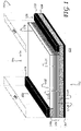
FIG. 1 schematically shows an exampleupright PV cell 102 including asubstrate 104. A PV cell is 'upright' (as opposed to 'inverted') if configured to be insolated through the layers deposited on the substrate, such that the incident light passes first through the last layer deposited (i.e., the front layer), then through the next-to-last layer and so on, and finally down to the substrate. (By contrast, in an inverted PV cell, the substrate supporting the layer-by-layer epitaxy is ultimately removed, providing a structure in which incident light passes through the layers in the reverse order; an inactive carrier substate is bonded to the last-deposited epitaxial layer for mechanical support.) Accordingly,upright PV cell 102 ofFIG. 1 is configured to be insolated onfront side 106, through various layers to be described presently. In the examples herein,substrate 104 can comprise a semiconductor-e.g., a die portion of a semiconductor wafer. Semiconductor materials suitable forsubstrate 104 include silicon, germanium, alloys thereof, and various III,V semiconductors and alloys, such as indium phosphide, gallium arsenide, and indium-gallium phosphide. It will be understood that these examples and others listed in this disclosure are provided for the sake of illustration and are not intended to be limiting in any sense. - Continuing in
FIG. 1 ,mesa 108 is arranged onsubstrate 104. Generally speaking, the mesa includes one or more epitaxial layers 110 grown onsubstrate 104. In the example shown inFIG. 1 ,PV cell 102 is a multi-junction PV cell, where the one or more epitaxial layers comprise dissimilar material layers. The mesa defines, relative to the substrate, a diffusedactive junction 112A. In effect, the diffused active junction is the interface betweensubstrate 104 and firstepitaxial layer 110A of the mesa. An 'active' junction, by virtue of its built-in voltage, actively separates electron-hole pairs generated by absorption of light in proximity to the junction. This diffused active junction is formed directly on the substrate. The mesa also defines, in view of its layer structure, one or more additional active junctions 112 situated above diffusedactive junction 112A. The number of active junctions ofPV cell 102 is not particularly limited. In some examples three or four junctions may provide an acceptable trade-off between energy-conversion efficiency and fabrication complexity. - Top
epitaxial layer 110Z ofmesa 108 can comprise a semiconductor material having the widest band gap of any semiconductor material ofPV cell 102. For instance,top epitaxial layer 110Z can comprise gallium nitride with a band gap of 3.44 electron-volts (eV), or gallium phosphide with a band gap of 2.26 eV. Electron-hole pairs generated by absorption of short-wavelength light within and directly belowepitaxial layer 110Z are separated atactive junction 112Z, which has a high built-in voltage. Longer-wavelength light may pass through toepitaxial layer 110A, comprising a semiconductor material having a band gap narrower than the band gap ofepitaxial layer 110Z but wider than the band gap of the substrate. For instance,epitaxial layer 110A can comprise gallium arsenide, with a band gap of 1.43 eV. Electron-hole pairs generated by absorption of longer-wavelength light within and directly aboveepitaxial layer 110A are separated atactive junction 112B, which has high built-in voltage lower thanactive junction 112Z. Light of still longer wavelength may pass through tosubstrate 104, comprising a semiconductor material having the lowest band gap of any semiconductor material ofPV cell 102. For instance, the substrate can comprise germanium with a band gap of 0.67 eV. The substrate can be 'active' in the sense that it is configured to absorb photons that pass throughmesa 108 and to accumulate charge carriers created in the substrate when such photons are absorbed. - In some examples, as shown in
FIG. 1 ,mesa 108 can include additional, intermediate epitaxial layers with band gaps arranged wide to narrow fromepitaxial layer 110Z tosubstrate 104. In some examples, the mesa can also include various barrier layers and associated junctions configured to modify the electric-potential gradient through the mesa, so as to increase the efficiency of charge-carrier transport. - Continuing in
FIG. 1 ,mesa 108 includes firstanti-reflective layer 114 andcap layer 116. The first anti-reflective layer may comprise a layer of predetermined thickness and/or refractive index configured to quell reflection of the insolation over a predetermined range of angles. The composition of the first anti-reflective layer is not particularly limited. The cap layer is a highly doped layer of whichever semiconductor comprises topepitaxial layer 110Z. In other words, in the non-limiting example in which the top layer is gallium arsenide, a highly doped gallium-arsenide cap layer is provided as an interface between the top epitaxial layer and the contact material (typically comprising one or more metals, vide infra). The mesa can also include a second, similarly configured anti-reflective layer arranged over the first anti-reflective layer (not shown inFIG. 1 ). -
Substrate 104 ofPV cell 102 includes a substrate-contact region 118 wherefirst contact 120 is arranged. Likewise,mesa 108 includes a mesa-contact region 122 wheresecond contact 124 is arranged. The substrate-contact region is exposed atbase 126 of the mesa. In the example illustrated inFIG. 1 ,base 126 is situated at one end of the mesa, and mesa-contact region 122 is situated at the opposite end of the mesa. -
First contact 120 andsecond contact 124 are both arranged onfront side 106 ofPV cell 102. Both contacts are positioned above the active substrate (i.e., on the front side, from which insolation is received). In examples in whichsubstrate 104 is p-doped, the first contact can be the negative contact of the PV cell, and the second contact can be the positive contact of the PV cell. The reverse configuration can be used with n-doped substrates. Typically each of the first and second contacts are ohmic contacts. The first and second contacts are each comprised of acontact material 128.First contact 120 includes contact material deposited in substrate-contact region 118, onfront side 106 of the PV cell.Second contact 124 includes contact material deposited in mesa-contact region 122, also on the front side of the PV cell. The composition of the contact material is not particularly limited and may depend on the type of PV cell being fabricated. Generally speaking, the contact may comprise one or more metals. In some examples, the contact material may further comprise one or more metalloids or semiconductors that improve the contact quality or adherence of the contact to the underlying semiconductor. - In some examples, as shown in
FIG. 1 , athin metal film 130 can be arranged onsubstrate 104 onback side 132 ofPV cell 102. -
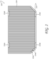
FIG. 2 shows an example PV cell 202 in plan view, as seen from the front side of the PV cell. The PV cells represented inFIGS. 1 and2 can be substantially the same in some examples, but may differ in other examples. In PV cell 202,gridlines 220 run down the front side tobusbar 233. In the illustrated example,busbar 233 is broadened into a plurality of first-polarity welding pads FIG. 2 also shows a plurality of second-polarity welding pads -
FIG. 3 shows anexample method 340 for fabricating an upright PV cell, andFIG. 4 schematically illustrates an evolving structure of an upright PV cell at selected stages of the method. For ease of understanding,method 340 is described with reference to the PV-cell configurations ofFIGS. 1 and2 . It will be understood, however, thatmethod 340 can be used to fabricate PV cells of different configurations. In some, non-limiting examples,method 340 can be applied to the fabrication of a 'thin' upright PV cell, which can be flexible, bendable, twistable, and/or rollable. As noted above in connection to the PV-cell configurations herein, a PV cell fabricated according tomethod 340 has both positive and negative contacts arranged on the front side. - At 342 of method 340 a suitable substrate for the PV cell-
substrate 404 inFIG. 4 -is prepared. The substrate may comprise a semiconductor as noted hereinabove. To that end, a semiconductor wafer can be sliced from a boule or obtained in any other manner. The wafer may comprise silicon, germanium, alloys thereof, or various III,V semiconductors and alloys, such as indium phosphide, gallium arsenide, and indium-gallium phosphide. The semiconductor wafer can be subject to mechanical, chemical, and/or plasma etching to expose a surface suitable for epitaxial deposition. - At 344 of
method 340 one or more epitaxial layers are grown on the prepared substrate. Layers can be deposited via state-of-the-art semiconductor fabrication methods. Such methods may include surface passivation, photolithography, ion implantation, dry etching, reactive-ion etching, atomic-layer etching, wet etching, plasma ashing, laser etching (or ablation), thermal oxidation, thermal annealing, chemical- and physical-vapor deposition, atomic-layer deposition, electrochemical deposition, and/or molecular-beam epitaxy. In growing the first of the one or more epitaxial layers, a diffused active junction is formed on the substrate, at 346. At 348, one or more additional active junctions are formed above the diffused active junction.FIG. 4 identifies diffusedactive junction 412A and an additionalactive junction 412N in the one or moreepitaxial layers 410. - At 350 an areal region of the one or more epitaxial layers is selectively etched. The areal region can be etched selectively via one or more of chemical etching, laser etching, plasma etching, mechanical etching, and saw cutting, as examples. Shown schematically in
FIG. 4 , selective etching ofareal region 452 forms amesa 408 on the substrate and exposes a substrate-contact region 418 parallel to the areal region, atbase 426 of the mesa. As noted hereinabove, the base can be arranged at one end of the mesa, and the mesa-contact region can be arranged at the opposite end of the mesa. In the example shown inFIG. 4 ,areal region 452 comprises an elongate strip. The elongate strip can extend from one side ofsubstrate 404 to the opposite side of the substrate (or substantially from one side ofsubstrate 404 to the opposite side of the substrate). In more particular examples, the elongate strip can be 100 µm (or about 100 µm) in width. In some examples selective etching of the areal region may comprise coating the one or more epitaxial layers with uncured resin and photochemically curing the regions outside of the areal region via a suitable photomask. Chemical and/or plasma etching can be used then to form the mesa. In other examples, a directed etch can be used. In some examples the areal region can be selectively etched down to the level of the substrate. - At 354 a first anti-reflective layer is deposited on the mesa, prior to deposition of contact material. First
anti-reflective layer 414 ofFIG. 4 can be deposited selectively, beginning with photolithographic protection of the mesa- and substrate-contact regions. The first anti-reflective layer can be deposited via chemical-vapor deposition (CVD), plasma-enhanced CVD (PECVD), or the like, and then the material deposited over the protected regions is removed. - At 356 a cap layer is grown on the mesa-contact region of the mesa.
Cap layer 416 ofFIG. 4 can be grown everywhere on the mesa and then subjected to a photoetch in which the cap layer is etched away outside of the mesa-contact region. Deposition and selective etching of the cap layer can be enacted via CVD, PECVD, etc. - At 358 of
method 340 contact material is deposited onto the substrate-contact region of the substrate, to form a first contact, and concertedly onto the mesa-contact region of the mesa, to form a second contact. The first and second contacts are of opposite polarity. In some examples, as shown inFIG. 4 ,contact material 428 can be deposited after suitable photomasking over the entire wafer. The contact material can be deposited via sputtering and/or thermal evaporation, for instance. These techniques can be used to form the first and second contacts concertedly. At 360 excess contact material is lifted off from of areas outside of the substrate- and mesa-contact regions, thereby definingfirst contact 420 andsecond contact 424. In some examples, the excess contact material can be lifted off via a laser lift-off procedure. The first contact can be narrower, after the lift-off procedure at 360, than the areal region selectively etched from the mesa at 350. Accordingly, the combined acts of selectively etching the mesa, depositing the contact material, and lifting off the excess contact material, can provide a standoff between the mesa and the first contact. In some examples the width of the standoff is 30 µm or wider. As described in further detail hereinafter, a standoff of sufficient width may provide protection against short-circuiting of the PV cell. In some examples, a second anti-reflective layer can deposited on the mesa after selective etching of the cap layer (at 356) and before depositing the contact material (at 358). - As shown in
FIG. 4 , the PV cell fabricated according tomethod 340 includes aback side 432 oppositefront side 406. At 362 the substrate thickness is reduced incrementally from the back side. The substrate thickness can be reduced in order to increase the efficiency of charge-carrier collection and to reduce the volume in which bulk recombination of charge carriers may occur. Typically the substrate thickness is reduced to a predetermined thickness. In some examples, the substrate is reduced to a thickness of between 25 and 225 µm. A substrate thickness at the upper end of this range is used in standard-thickness PV cells. A substrate thickness at the lower end of the range (e.g., 25 to 100 µm) is used for 'thin' PV cells. In some examples, the substrate thickness can be reduced by mechanical abrasion (i.e., grinding) from the back side of the PV cell. - At 364 of method 340 a metal film-
metal film 430 inFIG. 4 -is deposited onto the substrate fromback side 432 of the PV cell. The metal film can be deposited by thermal evaporation, sputtering, CVD, or PECVD, as examples. - As noted hereinabove the substrate may comprise a portion of a wafer. At 366 the wafer, with the mesa and the contact material deposited thereon, is sintered in order to consolidate the contact material. At 368 the wafer, with the mesa and the contact material deposited thereon, is diced to singulate and release the PV cell (
PV cell 402 inFIG. 4 ) from the wafer. - Upright PV cells as illustrated in
FIGS. 1 and2 , and as fabricated according to the method ofFIG. 3 , provide certain advantages over upright PV cells that have contacts on the back side of the cell. - First, it will be noted that the overall process flow of
FIG. 3 includes the same number of steps that would be used to fabricate an upright PV cell having front and back contacts. This is because the first and second contacts are formed concurrently atstep 358 of the method. Thus, the method ofFIG. 3 can be enacted with very little additional fabrication time or expense, relative to methods for fabricating upright PV cells having front and back contacts. - Significantly, the type of PV cell illustrated in
FIGS. 1 and2 , and as fabricated according to the method ofFIG. 3 , can be integrated into a solar panel comprising multiple plural PV cells with no need to weld onto the back side of any cell. Rather, the welding operation can be limited to joining the multiple negative contacts, arranged on the front side, and to joining the multiple positive contacts, also arranged on the front side. As noted hereinabove, the front side of a PV cell is typically more resistant than the back side to mechanical and thermal stresses associated with the welding operation. In preliminary results, the PV-cell failure rate for integration of one type of PV cell dropped from 22%, for cells having front and back contacts, to near 0% for cells fabricated according to the method ofFIG. 3 . Furthermore, in PV cells that survive the back-side weld process intact, the weld itself may impart significant thermal-expansion stress to the back of the cell, which may cause separation of the weld during panel operation. Further still, elimination of the back-side weld reduces cycle time and, in some cases, labor costs for solar-cell manufacture. - It was also determined, in this study, that the very low failure rate of PV cells fabricated according to the method of
FIG. 3 is somewhat correlated to the width of the standoff reserved at the base of the mesa of a PV cell (width S inFIG. 1 ). The failure rate was about 10% lower for PV cells in which a width of 100 µm is reserved relative to analogous PV cells in which the reserved width is only 30 µm. The reserved width is referred to hereinabove asareal region 452. Without tying this result to any particular theory, it is possible that areal-region widths on the narrower end of the 30-to-100 µm range may allow contact material of the first (substrate) contact to touch one or more layers of the mesa, thereby creating a low-resistance shunt across the PV cell. - Upright PV cells fabricated according to the method of
FIG. 3 have figures of merit (open-circuit voltages, short-circuit currents (Jsc), and fill factors) approaching those of otherwise similar upright PV cells with front and back contacts. In one study a small reduction in Jsc was observed. By inference, that effect can be attributed to the presence of additional, opaque contact material arranged on the front side of the PV cell. In many scenarios, the tradeoff of slightly lower Jsc in exchange for significantly reduced weld attrition and other benefits is an overall advantage. - Further, the disclosure comprise examples according to the following clauses:
- Clause 1. A method for fabricating an upright photovoltaic cell having a front side and first and second contacts arranged on the front side, the method comprising: growing one or more epitaxial layers on a substrate, thereby forming a diffused active junction on the substrate and one more additional active junctions above the diffused active junction; selectively etching an areal region of the one or more epitaxial layers, thereby forming a mesa on the substrate and exposing a substrate-contact region parallel to the areal region at a base of the mesa; and depositing contact material onto the substrate-contact region, to form the first contact, and concertedly onto a mesa-contact region of the mesa, to form the second contact.
- Clause 2. The method of claim 1, wherein selectively etching the areal region includes etching one or more of chemical etching, laser etching, and mechanical etching.
- Clause 3. The method of claim 1 or 2, wherein the base is at one end of the mesa, and the mesa-contact region is at an opposite end of the mesa.
- Clause 4. The method of any of claims 1-3, further comprising depositing a first anti-reflective layer on the mesa before depositing the contact material.
- Clause 5. The method of any of claims 1-4, further comprising growing a cap layer on the mesa and selectively etching the cap layer outside of the mesa-contact region.
- Clause 6. The method of any of claims 1-5, wherein depositing the contact material comprises depositing via concerted evaporation of the contact material onto the substrate-contact region and onto the mesa-contact region.
- Clause 7. The method of any of claims 1-6, further comprising lifting off the contact material outside of the substrate- and mesa-contact regions, wherein etching the mesa, depositing the contact material, and lifting off the contact material provides a standoff between the mesa and the first contact.
- Clause 8. The method of claim 7, wherein the standoff is 30 micrometers or wider.
- Clause 9. The method of any of claims 1-8, wherein the photovoltaic cell includes a back side opposite the front side, the method further comprising grinding the substrate to predetermined thickness from the back side.
- Clause 10. The method of claim 9, further comprising depositing a metal film on the substrate from the back side.
- Clause 11. The method of any of claims 1-10, wherein the substrate comprises a portion of a wafer, the method further comprising sintering the wafer with the mesa and the contact material to consolidate the contact material.
- Clause 12. The method of claim 11, further comprising dicing the wafer with the mesa and the contact material to singulate the photovoltaic cell from the wafer.
- Clause 13. An upright photovoltaic cell comprising: a substrate; a mesa including one or more epitaxial layers grown on the substrate, the mesa defining: a diffused active junction with the substrate, one or more additional active junctions above the diffused active junction, a mesa-contact region on the mesa, and a substrate-contact region exposed at a base of the mesa; a first contact including contact material deposited in the substrate-contact region, on a front side of the photovoltaic cell; and a second contact including the contact material deposited in the mesa-contact region, on the front side of the photovoltaic cell.
- Clause 14. The photovoltaic cell of claim 13, wherein the photovoltaic cell comprises a multi-junction photovoltaic cell, and wherein the one or more epitaxial layers comprise dissimilar material layers.
- Clause 15. The photovoltaic cell of any of claim 13 or 14, wherein the first contact is a negative contact of the photovoltaic cell, and the second contact is a positive contact of the photovoltaic cell.
- Clause 16. The photovoltaic cell of any of claims 13-15, wherein the base is at one end of the mesa, and the mesa-contact region is at an opposite end of the mesa.
- Clause 17. The photovoltaic cell of any of claims 13-16, wherein the substrate comprises a semiconductor substrate.
- Clause 18. The photovoltaic cell of any of claims 13-17, wherein the substrate is reduced to a thickness of between 25 and 225 micrometers.
- Clause 19. A method for fabricating a thin, upright photovoltaic cell having a front side, a back side opposite the front side, and first and second contacts arranged on the front side, the method comprising: growing one or more epitaxial layers on a semiconductor substrate, thereby forming a diffused active junction on the substrate and one more additional active junctions above the diffused active junction; selectively etching an areal region of the one or more epitaxial layers, thereby forming a mesa on the substrate and exposing a substrate-contact region parallel to the areal region at a base of the mesa; depositing contact material onto the substrate-contact region, to form the first contact, and concertedly onto a mesa-contact region of the mesa, to form the second contact; and grinding the substrate to predetermined thickness from the back side.
- Clause 20. The method of claim 19 further comprising depositing a thin metal film to the substrate from the back side.
- It will be understood that the configurations and/or approaches described herein are exemplary in nature, and that these specific examples are not to be considered in a limiting sense, because numerous variations are possible. The specific routines or processes described herein may represent one or more of any number of processing strategies. As such, various acts illustrated and/or described may be performed in the sequence illustrated and/or described, in other sequences, in parallel, or omitted. Likewise, the order of the above-described processes may be changed.
- The subject matter of the present disclosure includes all novel and non-obvious combinations and sub-combinations of the various processes, systems and configurations, and other features, functions, acts, and/or properties disclosed herein, as well as any and all equivalents thereof.
Claims (15)
- A method (340) for fabricating an upright photovoltaic cell (102) having a front side (106) and first and second contacts (120, 124) arranged on the front side, the method comprising:growing (344) one or more epitaxial layers (110) on a substrate (104), thereby forming a diffused active junction (112A) on the substrate and one more additional active junctions (112) above the diffused active junction;selectively etching (350) an areal region (452) of the one or more epitaxial layers, thereby forming a mesa (108) on the substrate and exposing a substrate-contact region (118) parallel to the areal region at a base (126) of the mesa; anddepositing (358) contact material (128) onto the substrate-contact region, to form the first contact, and concertedly onto a mesa-contact region (122) of the mesa, to form the second contact.
- The method of claim 1, wherein selectively etching the areal region includes etching one or more of chemical etching, laser etching, and mechanical etching.
- The method of claim 1 or 2, wherein the base is at one end of the mesa, and the mesa-contact region is at an opposite end of the mesa.
- The method of any of claims 1-3, further comprising depositing (354) a first anti-reflective layer (114) on the mesa before depositing the contact material.
- The method of any of claims 1-4, further comprising growing (356) a cap layer on the mesa and selectively etching (356) the cap layer outside of the mesa-contact region.
- The method of any of claims 1-5, wherein depositing the contact material comprises depositing via concerted evaporation of the contact material onto the substrate-contact region and onto the mesa-contact region.
- The method of any of claims 1-6 further comprising lifting off (360) the contact material outside of the substrate- and mesa-contact regions, wherein etching the mesa, depositing the contact material, and lifting off the contact material provides a standoff (S) between the mesa and the first contact and, optionally, wherein the standoff is optionally 30 micrometers or wider.
- The method of any of claims 1-7, wherein the photovoltaic cell includes a back side (132) opposite the front side, the method further comprising grinding (362) the substrate to predetermined thickness from the back side and, optionally, depositing (364) a metal film (130) on the substrate from the back side.
- The method of any of claims 1-8 wherein the substrate comprises a portion of a wafer, the method further comprising sintering (366) the wafer with the mesa and the contact material to consolidate the contact material and, optionally, dicing (368) the wafer with the mesa and the contact material to singulate the photovoltaic cell from the wafer.
- An upright photovoltaic cell (120) comprising:a substrate (104);a mesa (108) including one or more epitaxial layers (110) grown on the substrate, the mesa defining:a diffused active junction (112A) with the substrate,one or more additional active junctions (112) above the diffused active junction, a mesa-contact region (122) on the mesa, anda substrate-contact region (118) exposed at a base (126) of the mesa;a first contact (120) including contact material (128) deposited in the substrate-contact region, on a front side (106) of the photovoltaic cell; anda second contact (124) including the contact material deposited in the mesa-contact region, on the front side of the photovoltaic cell.
- The photovoltaic cell of claim 10, wherein the photovoltaic cell comprises a multi-junction photovoltaic cell, and wherein the one or more epitaxial layers comprise dissimilar material layers.
- The photovoltaic cell of claim 10 or 11, wherein the first contact is a negative contact of the photovoltaic cell, and the second contact is a positive contact of the photovoltaic cell.
- The photovoltaic cell of any of claims 10-12, wherein the base is at one end of the mesa, and the mesa-contact region is at an opposite end of the mesa.
- The photovoltaic cell of any of claims 10-13, wherein the substrate comprises a semiconductor substrate.
- The photovoltaic cell of any of claims 10-14, wherein the substrate is reduced to a thickness of between 25 and 225 micrometers.
Applications Claiming Priority (1)
| Application Number | Priority Date | Filing Date | Title |
|---|---|---|---|
| US17/449,421 US12245444B2 (en) | 2021-09-29 | 2021-09-29 | Upright photovoltaic cell with front contacts |
Publications (1)
| Publication Number | Publication Date |
|---|---|
| EP4160698A1 true EP4160698A1 (en) | 2023-04-05 |
Family
ID=82748386
Family Applications (1)
| Application Number | Title | Priority Date | Filing Date |
|---|---|---|---|
| EP22187288.0A Pending EP4160698A1 (en) | 2021-09-29 | 2022-07-27 | Upright photovoltaic cell with front contacts |
Country Status (3)
| Country | Link |
|---|---|
| US (1) | US12245444B2 (en) |
| EP (1) | EP4160698A1 (en) |
| JP (1) | JP2023050093A (en) |
Families Citing this family (1)
| Publication number | Priority date | Publication date | Assignee | Title |
|---|---|---|---|---|
| US12245444B2 (en) * | 2021-09-29 | 2025-03-04 | The Boeing Company | Upright photovoltaic cell with front contacts |
Citations (2)
| Publication number | Priority date | Publication date | Assignee | Title |
|---|---|---|---|---|
| US20140097522A1 (en) * | 2012-10-10 | 2014-04-10 | Solar Junction Corporation | Methods and apparatus for identifying and reducing semiconductor failures |
| CN112701176A (en) * | 2021-03-23 | 2021-04-23 | 南昌凯迅光电有限公司 | Gallium arsenide thin film solar cell and manufacturing method thereof |
Family Cites Families (10)
| Publication number | Priority date | Publication date | Assignee | Title |
|---|---|---|---|---|
| US7732706B1 (en) * | 2004-09-17 | 2010-06-08 | The United States Of America As Represented By The Administrator Of The National Aeronautics And Space Administration | Solar cell circuit and method for manufacturing solar cells |
| EP2372784B1 (en) * | 2010-03-29 | 2015-10-07 | Airbus DS GmbH | Solar cell, especially a multi-junction solar cell, for space applications |
| US8912617B2 (en) * | 2011-10-27 | 2014-12-16 | Solar Junction Corporation | Method for making semiconductor light detection devices |
| WO2014005102A1 (en) | 2012-06-28 | 2014-01-03 | Microlink Devices, Inc. | High efficiency, lightweight, flexible solar sheets |
| FR3004002B1 (en) * | 2013-03-29 | 2016-09-02 | Soitec Silicon On Insulator | PROCESS FOR ADVANCED ASSEMBLY OF CONCENTRATED PHOTOVOLTAIC CELL |
| DE102015009004A1 (en) * | 2015-06-05 | 2016-12-08 | Solaero Technologies Corp. | Automated arrangement and mounting of solar cells on panels for space applications |
| US20200313013A1 (en) * | 2019-04-01 | 2020-10-01 | The Boeing Company | Gallium arsenide solar cell having a fused silica cover |
| US20200313028A1 (en) * | 2019-04-01 | 2020-10-01 | The Boeing Company | Multijunction solar cell having a fused silica cover glass |
| US20200335648A1 (en) | 2019-04-19 | 2020-10-22 | The Boeing Company | Single toe interconnect |
| US12245444B2 (en) * | 2021-09-29 | 2025-03-04 | The Boeing Company | Upright photovoltaic cell with front contacts |
-
2021
- 2021-09-29 US US17/449,421 patent/US12245444B2/en active Active
-
2022
- 2022-07-26 JP JP2022118483A patent/JP2023050093A/en active Pending
- 2022-07-27 EP EP22187288.0A patent/EP4160698A1/en active Pending
Patent Citations (2)
| Publication number | Priority date | Publication date | Assignee | Title |
|---|---|---|---|---|
| US20140097522A1 (en) * | 2012-10-10 | 2014-04-10 | Solar Junction Corporation | Methods and apparatus for identifying and reducing semiconductor failures |
| CN112701176A (en) * | 2021-03-23 | 2021-04-23 | 南昌凯迅光电有限公司 | Gallium arsenide thin film solar cell and manufacturing method thereof |
Also Published As
| Publication number | Publication date |
|---|---|
| US12245444B2 (en) | 2025-03-04 |
| US20230335653A1 (en) | 2023-10-19 |
| JP2023050093A (en) | 2023-04-10 |
Similar Documents
| Publication | Publication Date | Title |
|---|---|---|
| US7785989B2 (en) | Growth substrates for inverted metamorphic multijunction solar cells | |
| US7960201B2 (en) | String interconnection and fabrication of inverted metamorphic multijunction solar cells | |
| US8187907B1 (en) | Solder structures for fabrication of inverted metamorphic multijunction solar cells | |
| US9018521B1 (en) | Inverted metamorphic multijunction solar cell with DBR layer adjacent to the top subcell | |
| CN101207078B (en) | Inverted metamorphic solar cell with bypass diode | |
| US9287431B2 (en) | Superstrate sub-cell voltage-matched multijunction solar cells | |
| US10069033B2 (en) | Integration of epitaxial lift-off solar cells with mini-parabolic concentrator arrays via printing method | |
| US20100186804A1 (en) | String Interconnection of Inverted Metamorphic Multijunction Solar Cells on Flexible Perforated Carriers | |
| US20110041898A1 (en) | Back Metal Layers in Inverted Metamorphic Multijunction Solar Cells | |
| US20100047959A1 (en) | Epitaxial Lift Off on Film Mounted Inverted Metamorphic Multijunction Solar Cells | |
| US20100229913A1 (en) | Contact Layout and String Interconnection of Inverted Metamorphic Multijunction Solar Cells | |
| US20140342494A1 (en) | Ohmic n-contact formed at low temperature in inverted metamorphic multijunction solar cells | |
| US20100206365A1 (en) | Inverted Metamorphic Multijunction Solar Cells on Low Density Carriers | |
| US20100093127A1 (en) | Inverted Metamorphic Multijunction Solar Cell Mounted on Metallized Flexible Film | |
| US11961931B2 (en) | Inverted metamorphic multijunction solar cells having a permanent supporting substrate | |
| JP2008166794A (en) | Inverted metamorphic solar cell mounted on a flexible membrane | |
| CA2801261A1 (en) | Photovoltaic component for use under concentrated solar flux | |
| EP4160698A1 (en) | Upright photovoltaic cell with front contacts | |
| US11398575B2 (en) | Back-contact thin film semiconductor device structures and methods for their production | |
| US8772079B2 (en) | Backside contacting on thin layer photovoltaic cells | |
| EP3127165B1 (en) | Method to manufacture epitaxial lift-off processed thin-film solar cells integrated with non-tracking mini-compound parabolic concentrators | |
| EP3872868B1 (en) | Multijunction solar cells for low temperature operation | |
| US20230327045A1 (en) | Multijunction solar cells with light scattering layer | |
| EP2439789B1 (en) | Inverted multijunction solar cells with group IV/III-V hybrid alloys | |
| WO2014055620A1 (en) | Methods for fabricating solar pv cells |
Legal Events
| Date | Code | Title | Description |
|---|---|---|---|
| PUAI | Public reference made under article 153(3) epc to a published international application that has entered the european phase |
Free format text: ORIGINAL CODE: 0009012 |
|
| STAA | Information on the status of an ep patent application or granted ep patent |
Free format text: STATUS: THE APPLICATION HAS BEEN PUBLISHED |
|
| AK | Designated contracting states |
Kind code of ref document: A1 Designated state(s): AL AT BE BG CH CY CZ DE DK EE ES FI FR GB GR HR HU IE IS IT LI LT LU LV MC MK MT NL NO PL PT RO RS SE SI SK SM TR |
|
| STAA | Information on the status of an ep patent application or granted ep patent |
Free format text: STATUS: REQUEST FOR EXAMINATION WAS MADE |
|
| 17P | Request for examination filed |
Effective date: 20230918 |
|
| RBV | Designated contracting states (corrected) |
Designated state(s): AL AT BE BG CH CY CZ DE DK EE ES FI FR GB GR HR HU IE IS IT LI LT LU LV MC MK MT NL NO PL PT RO RS SE SI SK SM TR |