EP4160684A1 - Display device - Google Patents
Display device Download PDFInfo
- Publication number
- EP4160684A1 EP4160684A1 EP22196327.5A EP22196327A EP4160684A1 EP 4160684 A1 EP4160684 A1 EP 4160684A1 EP 22196327 A EP22196327 A EP 22196327A EP 4160684 A1 EP4160684 A1 EP 4160684A1
- Authority
- EP
- European Patent Office
- Prior art keywords
- line
- voltage
- transistor
- initialization voltage
- transmission line
- Prior art date
- Legal status (The legal status is an assumption and is not a legal conclusion. Google has not performed a legal analysis and makes no representation as to the accuracy of the status listed.)
- Pending
Links
Images









Classifications
-
- H—ELECTRICITY
- H10—SEMICONDUCTOR DEVICES; ELECTRIC SOLID-STATE DEVICES NOT OTHERWISE PROVIDED FOR
- H10K—ORGANIC ELECTRIC SOLID-STATE DEVICES
- H10K59/00—Integrated devices, or assemblies of multiple devices, comprising at least one organic light-emitting element covered by group H10K50/00
- H10K59/10—OLED displays
- H10K59/12—Active-matrix OLED [AMOLED] displays
- H10K59/131—Interconnections, e.g. wiring lines or terminals
-
- H—ELECTRICITY
- H10—SEMICONDUCTOR DEVICES; ELECTRIC SOLID-STATE DEVICES NOT OTHERWISE PROVIDED FOR
- H10D—INORGANIC ELECTRIC SEMICONDUCTOR DEVICES
- H10D86/00—Integrated devices formed in or on insulating or conducting substrates, e.g. formed in silicon-on-insulator [SOI] substrates or on stainless steel or glass substrates
- H10D86/40—Integrated devices formed in or on insulating or conducting substrates, e.g. formed in silicon-on-insulator [SOI] substrates or on stainless steel or glass substrates characterised by multiple TFTs
- H10D86/441—Interconnections, e.g. scanning lines
- H10D86/443—Interconnections, e.g. scanning lines adapted for preventing breakage, peeling or short circuiting
-
- H—ELECTRICITY
- H10—SEMICONDUCTOR DEVICES; ELECTRIC SOLID-STATE DEVICES NOT OTHERWISE PROVIDED FOR
- H10D—INORGANIC ELECTRIC SEMICONDUCTOR DEVICES
- H10D86/00—Integrated devices formed in or on insulating or conducting substrates, e.g. formed in silicon-on-insulator [SOI] substrates or on stainless steel or glass substrates
- H10D86/40—Integrated devices formed in or on insulating or conducting substrates, e.g. formed in silicon-on-insulator [SOI] substrates or on stainless steel or glass substrates characterised by multiple TFTs
- H10D86/411—Integrated devices formed in or on insulating or conducting substrates, e.g. formed in silicon-on-insulator [SOI] substrates or on stainless steel or glass substrates characterised by multiple TFTs characterised by materials, geometry or structure of the substrates
-
- H—ELECTRICITY
- H10—SEMICONDUCTOR DEVICES; ELECTRIC SOLID-STATE DEVICES NOT OTHERWISE PROVIDED FOR
- H10D—INORGANIC ELECTRIC SEMICONDUCTOR DEVICES
- H10D86/00—Integrated devices formed in or on insulating or conducting substrates, e.g. formed in silicon-on-insulator [SOI] substrates or on stainless steel or glass substrates
- H10D86/40—Integrated devices formed in or on insulating or conducting substrates, e.g. formed in silicon-on-insulator [SOI] substrates or on stainless steel or glass substrates characterised by multiple TFTs
- H10D86/441—Interconnections, e.g. scanning lines
-
- H—ELECTRICITY
- H10—SEMICONDUCTOR DEVICES; ELECTRIC SOLID-STATE DEVICES NOT OTHERWISE PROVIDED FOR
- H10D—INORGANIC ELECTRIC SEMICONDUCTOR DEVICES
- H10D86/00—Integrated devices formed in or on insulating or conducting substrates, e.g. formed in silicon-on-insulator [SOI] substrates or on stainless steel or glass substrates
- H10D86/40—Integrated devices formed in or on insulating or conducting substrates, e.g. formed in silicon-on-insulator [SOI] substrates or on stainless steel or glass substrates characterised by multiple TFTs
- H10D86/60—Integrated devices formed in or on insulating or conducting substrates, e.g. formed in silicon-on-insulator [SOI] substrates or on stainless steel or glass substrates characterised by multiple TFTs wherein the TFTs are in active matrices
-
- H—ELECTRICITY
- H10—SEMICONDUCTOR DEVICES; ELECTRIC SOLID-STATE DEVICES NOT OTHERWISE PROVIDED FOR
- H10K—ORGANIC ELECTRIC SOLID-STATE DEVICES
- H10K59/00—Integrated devices, or assemblies of multiple devices, comprising at least one organic light-emitting element covered by group H10K50/00
- H10K59/10—OLED displays
- H10K59/12—Active-matrix OLED [AMOLED] displays
- H10K59/121—Active-matrix OLED [AMOLED] displays characterised by the geometry or disposition of pixel elements
-
- H—ELECTRICITY
- H10—SEMICONDUCTOR DEVICES; ELECTRIC SOLID-STATE DEVICES NOT OTHERWISE PROVIDED FOR
- H10K—ORGANIC ELECTRIC SOLID-STATE DEVICES
- H10K59/00—Integrated devices, or assemblies of multiple devices, comprising at least one organic light-emitting element covered by group H10K50/00
- H10K59/10—OLED displays
- H10K59/12—Active-matrix OLED [AMOLED] displays
- H10K59/121—Active-matrix OLED [AMOLED] displays characterised by the geometry or disposition of pixel elements
- H10K59/1213—Active-matrix OLED [AMOLED] displays characterised by the geometry or disposition of pixel elements the pixel elements being TFTs
-
- G—PHYSICS
- G09—EDUCATION; CRYPTOGRAPHY; DISPLAY; ADVERTISING; SEALS
- G09G—ARRANGEMENTS OR CIRCUITS FOR CONTROL OF INDICATING DEVICES USING STATIC MEANS TO PRESENT VARIABLE INFORMATION
- G09G2300/00—Aspects of the constitution of display devices
- G09G2300/04—Structural and physical details of display devices
- G09G2300/0421—Structural details of the set of electrodes
- G09G2300/0426—Layout of electrodes and connections
-
- H—ELECTRICITY
- H10—SEMICONDUCTOR DEVICES; ELECTRIC SOLID-STATE DEVICES NOT OTHERWISE PROVIDED FOR
- H10K—ORGANIC ELECTRIC SOLID-STATE DEVICES
- H10K59/00—Integrated devices, or assemblies of multiple devices, comprising at least one organic light-emitting element covered by group H10K50/00
- H10K59/60—OLEDs integrated with inorganic light-sensitive elements, e.g. with inorganic solar cells or inorganic photodiodes
- H10K59/65—OLEDs integrated with inorganic image sensors
Definitions
- the present invention relates to a display device.
- a display device is a device that displays a screen, and includes a liquid crystal display (LCD), an organic light emitting diode (OLED), and the like.
- the display device is used in various electronic devices such as a mobile phone, a navigation device, a digital camera, an electronic book, a portable game machine, and various terminals.
- An organic light emitting diode (OLED) display includes two electrodes and an organic emission layer interposed therebetween. Electrons injected from one electrode and holes injected from another electrode are combined in the organic emission layer to generate excitons. The generated excitons are changed to a ground state from an exited state, releasing energy to emit light.
- OLED organic light emitting diode
- the organic light emitting diode display includes pixels including an organic light emitting diode as a self-emissive element, and transistors for driving the organic light emitting diode and at least one capacitor are formed in each pixel.
- the organic light emitting device may further include a voltage line to which a signal for driving pixels is applied, and a voltage transmission line for transmitting a signal to the voltage line. These voltage lines and voltage transmission lines may be connected at the edge of the display device, and in case that the connection structure is complicated, the region where the screen is not displayed (also called "a dead space”) may become larger.
- the present invention provides a display device according to the independent claim.
- the dependent claims describe preferred embodiments. Embodiments are to provide a display device capable of reducing a region in which an image is not displayed.
- the display device includes a substrate including a display area and a peripheral area; a first voltage line disposed on the display area of the substrate, a first voltage being applied to the first voltage line; a second voltage line disposed on the display area of the substrate and extending in a direction parallel to the first voltage line, a second voltage being applied to the second voltage line; a first voltage transmission line disposed on the peripheral area of the substrate and transmitting the first voltage; a second voltage transmission line disposed on the peripheral area of the substrate and transmitting the second voltage; a first bridge electrode disposed on the first edge of the substrate and connecting the first voltage line and the first voltage transmission line; and a second bridge electrode disposed on the second edge of the substrate and connecting the second voltage line and the second voltage transmission line.
- the first edge and the second edge may face each other.
- the first voltage and the second voltage may be constant, and the first voltage may be different from the second voltage.
- the substrate may have a polygonal shape.
- the substrate may have corner parts.
- Each corner part of the substrate may have a rounded shape, and the first bridge electrode and the second bridge electrode may be disposed at the each corner part.
- the first bridge electrode and the second bridge electrode may extend in a first direction, and the first voltage line, and the second voltage line may extend in a second direction perpendicular to the first direction.
- the first edge of the substrate may include a first corner part, a second corner part (these corner parts may be the same corner parts as described above), and a first straight-line part disposed between the first corner part and the second corner part;
- the second edge of the substrate may include a third corner part, a fourth corner part, and a second straight-line part disposed between the third corner part and the fourth corner part;
- the first bridge electrode may be disposed on the first corner part and the second corner part, and is not disposed on the third corner part and the fourth corner part; and the second bridge electrode may be disposed on the third corner part and the fourth corner part, and is not disposed on the first corner part and the second corner part.
- the first voltage line and the first voltage transmission line may be electrically connected over the first corner part and the second corner part, and may be electrically disconnected over the third corner part and the fourth corner part
- the second voltage line and the second voltage transmission line may be electrically connected over the third corner part and the fourth corner part, and may be electrically disconnected over the first corner part and the second corner part.
- the display device may further include a third bridge electrode disposed on the first straight-line part of the first edge of the substrate and electrically connecting the first voltage line and the first voltage transmission line; and a fourth bridge electrode disposed on the second straight-line part of the second edge of the substrate and electrically connecting the first voltage line and the first voltage transmission line.
- the third bridge electrode and the fourth bridge electrode may extend in the second direction, the first voltage transmission line and the second voltage transmission line may have a shape surrounding the display area in a plan view, and the first voltage transmission line may be disposed outside the second voltage transmission line.
- the second voltage line and the second voltage transmission line may be directly connected on the first straight-line part and the second straight-line part.
- the display device may further include a third bridge electrode disposed on the first straight-line part of the first edge of the substrate and electrically connecting the first voltage line and the first voltage transmission line, the third bridge electrode may extend in the second direction, the first voltage line and the first voltage transmission line may be electrically disconnected on the second straight-line part of the second edge of the substrate, the first voltage transmission line and the second voltage transmission line may have a shape surrounding the display area in a plan view, and the first voltage transmission line may be disposed outside the second voltage transmission line.
- the second voltage line and the second voltage transmission line may be directly connected on the second straight-line part, and electrically disconnected on the first straight-line part.
- the display device may further include a semiconductor layer disposed on the substrate and including a channel, a first region and a second region of a first transistor, a channel of a first region and a second region of a second transistor, and a channel, a first region, and a second region of a third transistor; a gate conductor including a gate electrode of the first transistor overlapping the channel of the first transistor in a plan view, a gate electrode of the second transistor overlapping the channel of the second transistor in a plan view, and a gate electrode of the seventh transistor overlapping the channel of the third transistor in a plan view; and a data conductor including a connection electrode electrically connecting a gate electrode of the first transistor and a second region of the second transistor.
- the first voltage line may be electrically connected to the first region of the second transistor, and the first voltage may be a first initialization voltage.
- the first voltage line and the data conductor may be disposed on a same layer.
- the first voltage transmission line and the data conductor may be disposed on a same layer.
- the second voltage line may be electrically connected to the second region of the third transistor, and the second voltage may be a second initialization voltage.
- the second voltage line and the data conductor may be disposed on a same layer.
- the second voltage transmission line and the data conductor may be disposed on a same layer.
- the first bridge electrode, the second bridge electrode, and the gate conductor may be disposed on a same layer.
- the display device may further include a data line and a driving voltage line extending in a direction parallel to the first voltage line and the second voltage line, and the data line, the driving voltage line, and the data conductor may be disposed on a same layer.
- the data line and the driving voltage line may be disposed between the first voltage line and the second voltage line in a plan view.
- the display device may include pixels, each the pixels may include the first transistor, the second transistor, and the third transistor, and the pixels may have a symmetrical shape with respect to the second voltage line.
- the region where an image is not displayed may be reduced in the display device.
- the phrase “on a plane” or “in a plan view” means viewing a target portion from the top
- the phrase “on a cross-section” means viewing a cross-section formed by vertically cutting a target portion from the side.
- At least one of is intended to include the meaning of "at least one selected from the group of” for the purpose of its meaning and interpretation.
- at least one of A and B may be understood to mean “A, B, or A and B.”
- FIG. 1 is a schematic plan view showing a display device according to an embodiment.
- a display device 1000 includes a substrate 110 and pixels PX positioned on (or disposed on) the substrate 110.
- the substrate 110 may include a first region A1, a second region A2, and a bending region BA positioned between the first region A1 and the second region A2.
- the substrate 110 may be made of a flexible material and may be changed into various shapes.
- the substrate 110 may be flexible, stretchable, foldable, bendable, or rollable.
- the bending region BA may be a region in which the substrate 110 is bent.
- the first region A1 and the second region A2 may have a flat shape. However, this is only an example, and the substrate 110 may additionally include a region to be bent. For example, at least a portion of the first region A1 or the second region A2 of the substrate 110 may be bent.
- the first region A1 of the substrate 110 extends from the bending region BA.
- the first region A1 may be approximately formed as a rectangle including a long side and a short side, and a corner portion may be chamfered to have a rounded shape.
- the shape of the first region A1 is only an example and may be changed to various shapes.
- the first region A1 may include a display area DA and a peripheral area PA.
- the display area DA may be positioned in the center of the first region A1, and may have a shape approximately similar to that of the first region A1.
- the peripheral area PA may surround the display area DA.
- the peripheral area PA may be positioned outside the first region A1.
- Pixels PX may be positioned in the display area DA. Pixels PX may be disposed in a matrix form, and may receive an image signal and display an image accordingly. In this case, the arrangement shape of pixels PX may be variously changed.
- the display device may further include signal lines.
- the signal lines may include scan lines, light emission control lines, data lines, first initialization voltage lines (also called as first voltage lines), second initialization voltage lines (also called as second voltage lines), driving voltage lines, and the like. Theses signal lines may transmit a scan signal, a light emission control signal, a data signal, a first initialization voltage, a second initialization voltage, a driving voltage, and the like.
- each pixel PX may include transistors, a capacitor, and at least one light-emitting diode (LED), which are electrically connected to signal lines.
- the display device according to an embodiment may be an organic light emitting device.
- the type of display device is not limited thereto, and various types of the display devices may be used.
- the display device may be formed as a liquid crystal display, an electrophoretic display, or an electrowetting display device.
- the display device may be a next-generation display device such as a micro light emitting diode (Micro LED) display device, a quantum dot light-emitting diode (QLED) display device, and a quantum dot organic light-emitting diode (QD-OLED) display device.
- a next-generation display device such as a micro light emitting diode (Micro LED) display device, a quantum dot light-emitting diode (QLED) display device, and a quantum dot organic light-emitting diode (QD-OLED) display device.
- Micro LED micro light emitting diode
- QLED quantum dot light-emitting diode
- QD-OLED quantum dot organic light-emitting diode
- a voltage transmission line for transmitting a voltage to signal lines may be positioned in the peripheral area PA.
- the voltage transmission line may be formed to surround the display area DA.
- the voltage transmission line may include a first initialization voltage transmission line (also called as first voltage transmission line), a second initialization voltage transmission line (also called as second voltage transmission line), and the like.
- the first initialization voltage transmission line may be electrically connected to the first initialization voltage line to transmit the first initialization voltage.
- the second initialization voltage transmission line may be electrically connected to the second initialization voltage line to transmit the second initialization voltage.
- the second region A2 of the substrate 110 extends from the bending region BA.
- the second region A2 is a non-display area that does not display an image and does not include pixels PX. Elements and/or wires for generating and/or transmitting various signals applied to the pixel PX are located in the second region A2.
- a driving circuit chip 250 and a flexible circuit board 200 may be positioned on the second region A2.
- the driving circuit chip 250 is electrically connected to the elements or wires positioned in the second region A2 to transmit various signals to pixels PX.
- the driving circuit chip 250 may supply a scan signal, a control signal, a data signal, and the like.
- the flexible circuit board 200 may be attached to the edge of the second region A2 of the substrate 110.
- the flexible circuit board 200 may be made of a flexible material.
- the flexible circuit board 200 has a circuit designed to control the operation of the display device.
- the bending region BA of the substrate 110 may be positioned between the first region A1 and the second region A2 to electrically connect the first region A1 to the second region A2. In case that the substrate 110 is bent, the first region A1 and the second region A2 may overlap each other.
- the bending region BA of the substrate 110 may be positioned so that it is connected (or extended) to a short side of the first region A1.
- the position of the bending region BA is only an example and may be variously changed.
- the bending region BA may be positioned so that it is connected to short sides of the first region A1, or it may be positioned so that it is connected to a long side of the first region A1.
- FIG. 2 is a schematic diagram of an equivalent circuit of a pixel of a display device according to an embodiment.
- the display device includes pixels PX capable of displaying an image and signal lines 127, 128, 151, 152, 154, 155, 171, and 172.
- a pixel PX includes transistors T1, T2, T3, T4, T5, T6, and T7 electrically connected to the signal lines 127, 128, 151, 152, 154, 155, 171, and 172, a capacitor Cst, and at least one light-emitting diode LED.
- a pixel PX includes a light-emitting diode LED.
- the signal lines 127, 128,151,152,154,155,171, and 172 may include a first initialization voltage line (or first voltage line) 127, a second initialization voltage line (or second voltage line) 128, scan lines 151, 152, and 154, a light emission control line 155, a data line 171, and a driving voltage line 172.
- the first initialization voltage line 127 may transmit a first initialization voltage VINT1
- the second initialization voltage line 128 may transmit a second initialization voltage VINT2.
- the scan lines 151, 152, and 154 may transmit scan signals GWn, GIn, and GI(n+1), respectively.
- the scan signals GWn, GIn, and GI(n+1) may transmit a gate-on voltage and a gate-off voltage that can turn on or off the transistors T2, T3, T4, and T7 included in the pixel PX.
- the scan lines 151, 152, and 154 electrically connected to a pixel PX may include a first scan line 151 capable of transmitting a scan signal GWn, a second scan line 152 capable of transmitting a scan signal GIn having a gate-on voltage at different timing from that of the first scan line 151, and a third scan line 154 capable of transmitting a scan signal GI(n+1).
- a first scan line 151 capable of transmitting a scan signal GWn
- a second scan line 152 capable of transmitting a scan signal GIn having a gate-on voltage at different timing from that of the first scan line 151
- a third scan line 154 capable of transmitting a scan signal GI(n+1).
- the scan signal GIn may be a previous scan signal such as an (n-1)-th scan signal S(n-1), and the scan signal GI(n+1) may be an n-th scan signal Sn.
- the embodiment is not limited thereto, and the scan signal GI(n+1) may be a different scan signal from the n-th scan signal Sn.
- the light emission control line 155 may transmit a control signal, and particularly may transmit a light emission control signal EM capable of controlling emission of the light-emitting diode LED included in the pixel PX.
- the control signal transmitted by the light emission control line 155 may consist of a gate-on voltage and a gate-off voltage, and may have a different waveform from the scan signal transmitted by the scan lines 151, 152, and 154.
- the data line 171 may transmit a data signal Dm, and the driving voltage line 172 may transmit a driving voltage ELVDD.
- the data signal Dm may have other voltage levels according to the image signal input to the display device, and the driving voltage ELVDD may have a substantially constant level.
- the display device may further include a driver for transmitting signals to signal lines 127,151, 152, 154, 155, 171, and 172.
- Transistors T1, T2, T3, T4, T5, T6, and T7 included in a pixel PX include a first transistor T1, a second transistor T2, a third transistor T3, a fourth transistor T4, a fifth transistor T5, a sixth transistor T6, and a seventh transistor T7.
- the first scan line 151 may transmit the scan signal GWn to the second transistor T2 and the third transistor T3, the second scan line 152 may transmit the scan signal GIn to the fourth transistor T4, the third scan line 154 may transmit the scan signal GI(n+1) to the seventh transistor T7, and the light emission control line 155 may transmit the light emission control signal EM to the fifth transistor T5 and the sixth transistor T6.
- a gate electrode G1 of the first transistor T1 is electrically connected to a first terminal of the capacitor Cst through a driving gate node GN, a first electrode Ea1 of the first transistor T1 is electrically connected to the driving voltage line 172 via the fifth transistor T5, and a second electrode Eb1 of the first transistor T1 is electrically connected to an anode of the light-emitting diode LED via the sixth transistor T6.
- the first transistor T1 may receive the data signal Dm transmitted by the data line 171 depending on the switching operation of the second transistor T2 to supply a driving current Id to the light-emitting diode LED.
- a gate electrode G2 of the second transistor T2 is electrically connected to the first scan line 151, a first electrode Ea2 of the second transistor T2 is electrically connected to the data line 171, and a second electrode Eb2 of the second transistor T2 is electrically connected to the first electrode Ea1 of the first transistor T1 and is electrically connected to the driving voltage line 172 via the fifth transistor T5.
- the second transistor T2 is turned on depending on the scan signal GWn transmitted through the first scan line 151, thereby transmitting the data signal Dm, transmitted from the data line 171, to the first electrode Ea1 of the first transistor T1.
- a gate electrode G3 of the third transistor T3 is electrically connected to the first scan line 151, and a first electrode Ea3 of the third transistor T3 is electrically connected to the second electrode Eb1 of the first transistor T1 and is electrically connected to the anode of the light-emitting diode LED via the sixth transistor T6.
- a second electrode Eb3 of the third transistor T3 is electrically connected to a second electrode Eb4 of the fourth transistor T4, the first terminal of the capacitor Cst, and the gate electrode G1 of the first transistor T1.
- the third transistor T3 is turned on depending on the scan signal GWn transmitted through the first scan line 151 to electrically connect the gate electrode G1 and the second electrode Eb1 of the first transistor T1 to each other, thereby electrically diode-connecting the first transistor T1.
- a gate electrode G4 of the fourth transistor T4 is electrically connected to the second scan line 152, a first electrode Ea4 of the fourth transistor T4 is electrically connected to the first initialization voltage line 127, and the second electrode Eb4 of the fourth transistor T4 is electrically connected to the first terminal of the capacitor Cst and the gate electrode G1 of the first transistor T1 through the second electrode Eb3 of the third transistor T3.
- the fourth transistor T4 is turned on depending on the scan signal GIn transmitted through the second scan line 152 to transmit the first initialization voltage VINT1 to the gate electrode G1 of the first transistor T1, thereby performing an initialization operation of initializing the voltage of the gate electrode G1 of the first transistor T1.
- a gate electrode G5 of the fifth transistor T5 is electrically connected to the light emission control line 155, a first electrode Ea5 of the fifth transistor T5 is electrically connected to the driving voltage line 172, and a second electrode Eb5 of the fifth transistor T5 is electrically connected to the first electrode Ea1 of the first transistor T1 and the second electrode Eb2 of the second transistor T2.
- a gate electrode G6 of the sixth transistor T6 is electrically connected to the light emission control line 155, a first electrode Ea6 of the sixth transistor T6 is electrically connected to the second electrode Eb1 of the first transistor T1 and the first electrode Ea3 of the third transistor T3, and a second electrode Eb6 of the sixth transistor T6 is electrically connected to the anode of the light-emitting diode LED.
- the fifth transistor T5 and the sixth transistor T6 are simultaneously turned on depending on the light emission control signal EM transmitted through the light emission control line 155, thereby transmitting the driving voltage ELVDD to the light-emitting diode LED through the diode-connected first transistor T1.
- a gate electrode G7 of the seventh transistor T7 is electrically connected to the third scan line 154, a first electrode Ea7 of the seventh transistor T7 is electrically connected to the second electrode Eb6 of the sixth transistor T6 and the anode of the light-emitting diode LED, and a second electrode Eb7 of the seventh transistor T7 is electrically connected to the second initialization voltage line 128.
- the seventh transistor T7 is turned on according to the scan signal GI(n+1) received through the third scan line 154 and transmits the second initialization voltage VINT2 to the anode of the light-emitting diode LED, thereby serving to initialize the anode of the light-emitting diode LED.
- different initialization voltages may be applied to the fourth transistor T4 and the seventh transistor T7.
- the first initialization voltage VINT1 may be applied to the fourth transistor T4
- the second initialization voltage VINT2 may be applied to the seventh transistor T7. Therefore, it is possible to improve the characteristic of the display device according to an embodiment.
- the transistors T1, T2, T3, T4, T5, T6, and T7 may be P-type channel transistors such as a P-channel metal oxide semiconductor (PMOS), but are not limited thereto, and at least one among the transistors T1, T2, T3, T4, T5, T6, and T7 may be an N-type channel transistor and may include both a P-type and an N-type channel transistor.
- PMOS P-channel metal oxide semiconductor
- the first terminal of the capacitor Cst is electrically connected to the gate electrode G1 of the first transistor T1 as described above and a second terminal is electrically connected to the driving voltage line 172.
- the cathode of the light-emitting diode LED is electrically connected to a common voltage ELVSS terminal that transmits a common voltage ELVSS, so that the common voltage ELVSS may be applied thereto.
- the structure of the pixel PX according to an embodiment is not limited to the structure shown in FIG. 2 , and the number of transistors and the number of capacitors included in a pixel PX and the connection relationship therebetween may be variously modified.
- FIG. 3 is a schematic plan view illustrating a part of a display device according to an embodiment
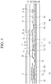
- FIG. 4 is a schematic cross-sectional view of a display device according to an embodiment taken along line IV-IV' of FIG. 3
- FIG. 5 is a schematic cross-sectional view of a display device according to an embodiment taken along line V-V' of FIG. 3
- FIGS. 6 to 8 are schematic plan views sequentially illustrating a display device according to an embodiment an according to a manufacturing order.
- FIGS. 3 to 8 illustrate two adjacent pixels positioned in the display area of a display device according to an embodiment. In this case, two adjacent pixels may have planar structures that are symmetrical to each other. However, the disclosure is not limited thereto, and two adjacent pixels may have a same planar structure.
- the display device may include a substrate 110.
- the substrate 110 may include at least one among polystyrene, polyvinyl alcohol, polymethyl methacrylate, polyethersulfone, polyacrylate, polyetherimide, polyethylene naphthalate, polyethylene terephthalate, polyphenylene sulfide, polyarylate, polyimide, polycarbonate, cellulose triacetate, and cellulose acetate propionate.
- the substrate 110 may be single-layered or multi-layered.
- the substrate 110 may have a structure in which at least one base layer and at least one inorganic layer, including a polymer resin sequentially stacked, are alternately stacked.
- a semiconductor layer including a channel 1132, a first region 1131, and a second region 1133 of the first transistor T1 may be positioned on the substrate 110.
- FIG. 6 illustrates a semiconductor layer.
- the semiconductor layer may further include a channel 4132, a first region 4131, and a second region 4133 of the fourth transistor T4, and a channel 7132, a first region 7131, and a second region 7133 of the seventh transistor T7 as well as the first transistor T1.
- the semiconductor layer may further include a channel, a first region, and a second region of each of the second transistor T2, the third transistor T3, the fifth transistor T5, and the sixth transistor T6.
- the channel 1132 of the first transistor T1 may have a U shape in a plan view.
- the channel 1132 may have a U shape in the length of the channel, this may be a U shape in a plane defined by the directions DR1 and DR2.
- the shape of the channel 1132 of the first transistor T1 is not limited thereto, and may be variously changed.
- the channel 1132 of the first transistor T1 may be bent into a different shape or may be formed into a bar shape.
- the first region 1131 and the second region 1133 of the first transistor T1 may be positioned on respective sides of the channel 1132 of the first transistor T1.
- the first region 1131 of the first transistor T1 may extend up and down in a plan view, so that a portion thereof extending downward may be electrically connected to the second region of the fifth transistor T5, and a portion thereof extending upward may be electrically connected to the second region of the second transistor T2.
- the second region 1133 of the first transistor T1 may extend up and down in a plan view, so that a portion thereof extending downward may be electrically connected to the first region of the sixth transistor T6, and a portion thereof extending upward may be electrically connected to the first region of the third transistor T3.
- the fourth transistor T4 may include two channels 4132, the first region 4131 may be positioned on a side of a channel 4132, and the second region 4133 may be positioned on a side of the other channel 4132.
- the second region 4133 of the fourth transistor T4 may extend downward in a plan view to be electrically connected to the second region of the third transistor T3.
- the first region 7131 and the second region 7133 of the seventh transistor T7 may be positioned on respective sides of the channel 7132 of the seventh transistor T7.
- the first region 7131 of the seventh transistor T7 may extend upward in a plan view to be electrically connected to the second region of the sixth transistor T6.
- a buffer layer 111 may be positioned between the substrate 110, and the semiconductor layer including the channel 1132, the first region 1131, and the second region 1133 of the first transistor T1, the channel 4132, the first region 4131, and the second region 4133 of the fourth transistor T4, and the channel 7132, the first region 7131, and the second region 7133 of the seventh transistor T7.
- the buffer layer 111 may have a single-layer or a multi-layered structure.
- the buffer layer 111 may include an inorganic insulating material or an organic insulating material such as a silicon nitride (SiN x ), a silicon oxide (SiO x ), or a silicon oxynitride (SiO x N y ).
- a barrier layer may be further positioned between the substrate 110 and the buffer layer 111.
- the barrier layer may have a single-layer or a multi-layered structure.
- the barrier layer may include an inorganic insulating material such as a silicon nitride (SiN x ), a silicon oxide (SiO x ), or a silicon oxynitride (SiO x N y ).
- a gate insulating layer 140 may be positioned on the semiconductor layer including the channel 1132, the first region 1131, and the second region 1133 of the first transistor T1, the channel 4132, the first region 4131, and the second region 4133 of the fourth transistor T4, and the channel 7132, the first region 7131, and the second region 7133 of the seventh transistor T7.
- the gate insulating layer 140 may have a single-layer or a multi-layered structure.
- the gate insulating layer 140 may include an inorganic insulating material such as a silicon nitride (SiN x ), a silicon oxide (SiO x ), or a silicon oxynitride (SiO x N y ).
- a gate conductor including a gate electrode 1151 of the first transistor T1 may be positioned on the gate insulating layer 140.
- FIG. 7 illustrates together the semiconductor layer and the gate conductor.
- the gate conductor may have a single-layer or a multi-layered structure.
- the gate conductor may include a metal material such as molybdenum (Mo), aluminum (Al), copper (Cu), and/or titanium (Ti).
- the gate conductor may further include a gate electrode 4151 of the fourth transistor T4 and a gate electrode 7151 of the seventh transistor T7 as well as the first transistor T1.
- the gate conductor may further include gate electrodes of each of the second transistor T2, the third transistor T3, the fifth transistor T5, and the sixth transistor T6.
- the gate electrode 1151 of the first transistor T1 may overlap the channel 1132 of the first transistor T1.
- the channel 1132 of the first transistor T1 is covered by the gate electrode 1151 of the first transistor T1.
- the gate electrode 4151 of the fourth transistor T4 may overlap the channel 4132 of the fourth transistor T4, and the gate electrode 7151 of the seventh transistor T7 may overlap the channel 7132 of the seventh transistor T7.
- the gate conductor may further include a first scan line 151, a second scan line 152, a third scan line 154, and a light emission control line 155.
- the first scan line 151, the second scan line 152, the third scan line 154, and the light emission control line 155 may extend in parallel to each other.
- the first scan line 151, the second scan line 152, the third scan line 154, and the light emission control line 155 may extend approximately in the first direction DR1.
- the first direction DR1 may be a row direction.
- the first scan line 151 may be electrically connected to the gate electrode of the second transistor T2 and the gate electrode of the third transistor T3, and may transmit the scan signal GWn.
- the first scan line 151 may be integral with (or may be formed integrally with) the gate electrode of the second transistor T2 and the gate electrode of the third transistor T3.
- the second scan line 152 may be electrically connected to the gate electrode 4151 of the fourth transistor T4, and may transmit the scan signal GIn.
- the second scan line 152 may be integral with the gate electrode 4151 of the fourth transistor T4.
- the second scan line 152 may be electrically connected to the gate electrode 7151 of the seventh transistor T7 positioned at the pixel of a previous stage.
- the third scan line 154 electrically connected to the seventh transistor T7 may be the first scan line at a rear stage.
- the light emission control line 155 is electrically connected to the gate electrode of the fifth transistor T5 and the gate electrode of the sixth transistor T6, and may transmit the light emission control signal EM.
- the light emission control line 155 may be integral with the gate electrode of the fifth transistor T5 and the gate electrode of the sixth transistor T6.
- a doping process or plasma treatment may be performed.
- Part of the semiconductor layer covered by (overlapped by or overlapping) the gate conductor is not doped or plasma-treated, and the part of the semiconductor layer that is not covered by the gate conductor is doped or plasma-treated, thereby having the same characteristic as a conductor. Accordingly, the first region and the second region of the first to seventh transistors T1, T2, T3, T4, T5, T6, and T7 of each semiconductor layer may become a first electrode and a second electrode.
- the doping process may be performed with a p-type dopant
- the first transistor T1, the second transistor T2, the third transistor T3, the fourth transistor T4, the fifth transistor T5, the sixth transistor T6, and the seventh transistor T7 may have a p-type transistor characteristic.
- An interlayer insulating layer 160 may be positioned on the gate conductor including the gate electrode 1151 of the first transistor T1, the gate electrode 4151 of the fourth transistor T4, and the gate electrode 7151 of the seventh transistor T7.
- the interlayer insulating layer 160 may have a single-layer or a multi-layered structure.
- the interlayer insulating layer 160 may include an inorganic insulating material or an organic insulating material.
- a data conductor including a first initialization voltage line 127 and a second initialization voltage line 128 may be positioned on the interlayer insulating layer 160.
- FIG. 8 illustrates the semiconductor layer, the gate conductor, and the data conductor together.
- the data conductor may have a single-layer or a multi-layered structure.
- the data conductor may include at least one of aluminum (Al), platinum (Pt), palladium (Pd), silver (Ag), magnesium (Mg), gold (Au), nickel (Ni), neodymium (Nd), iridium (Ir), chromium (Cr), nickel (Ni), calcium (Ca), molybdenum (Mo), titanium (Ti), tungsten (W), and/or copper (Cu).
- the first initialization voltage line 127 and the second initialization voltage line 128 may extend in a direction parallel to each other.
- the first initialization voltage line 127 and the second initialization voltage line 128 may extend in the second direction DR2.
- the second direction DR2 may be a column direction.
- the first initialization voltage line 127 and the second initialization voltage line 128 may not extend in the first direction DR1.
- an area occupied thereby in the display area DA is relatively reduced, so that the aperture ratio of the display device according to an embodiment may be improved.
- the first initialization voltage line 127 may run from an end to another end on the substrate 110 in a plan view.
- the first initialization voltage line 127 may run from an upper end to a lower end on the substrate 110 in a plan view.
- the pixels adjacent to each other in the second direction DR2 may be electrically connected to a same first initialization voltage line 127.
- the first initialization voltage line 127 is electrically connected to the first region 4131 of the fourth transistor T4, and may transmit the first initialization voltage VINT1.
- the interlayer insulating layer 160 may include an opening 163 overlapping the first region 4131 of the fourth transistor T4 and the first initialization voltage line 127. In this case, the opening 163 may also be formed in the gate insulating layer 140.
- the first initialization voltage line 127 may be electrically connected to the first region 4131 of the fourth transistor T4 through the opening 163.
- the second initialization voltage line 128 may run from an end to another end on the substrate 110 in a plan view.
- the second initialization voltage line 128 may run from an upper end to a lower end on the substrate 110 in a plan view.
- the pixels adjacent to each other in the second direction DR2 may be electrically connected to a same second initialization voltage line 128.
- the second initialization voltage line 128 is electrically connected to the second region 7133 of the seventh transistor T7, and may transmit the second initialization voltage VINT2.
- the interlayer insulating layer 160 may include an opening 161 that overlaps the second region 7133 of the seventh transistor T7 and the second initialization voltage line 128. In this case, the opening 161 may also be formed in the gate insulating layer 140.
- the second initialization voltage line 128 may be electrically connected to the second region 7133 of the seventh transistor T7 through the opening 161.
- Two pixels positioned on both sides of the second initialization voltage line 128 in a plan view may have planar structures symmetrical to each other
- the data conductor may further include a data line 171, a driving voltage line 172, a first connection electrode 175, and a second connection electrode 176.
- the data line 171 and the driving voltage line 172 may extend in a direction parallel to each other.
- the data line 171 and the driving voltage line 172 may extend in the second direction DR2. Accordingly, the data line 171 and the driving voltage line 172 may extend in parallel to the first initialization voltage line 127 and the second initialization voltage line 128.
- the data line 171 may run from an end to another end on the substrate 110 in a plan view.
- the data line 171 may run from an upper end to a lower end on the substrate 110 in a plan view.
- the pixels adjacent to each other in the second direction DR2 may be electrically connected to a same data line 171.
- the data line 171 may be electrically connected to the first region of the second transistor T2 and may transmit the data signal Dm.
- the driving voltage line 172 may run from an end to another end on the substrate 110 in a plan view.
- the driving voltage line 172 may run from an upper end to a lower end of the substrate 110 in a plan view.
- the pixels adjacent to each other in the second direction DR2 may be electrically connected to a same driving voltage line 172.
- the driving voltage line 172 may be electrically connected to the first region of the fifth transistor T5 and may transmit the driving voltage ELVDD.
- the driving voltage lines 172 adjacent to each other in the first direction DR1 may be electrically connected to each other. In this case, the adjacent driving voltage lines 172 may be electrically connected to each other by a separate electrode pattern positioned on a different layer from the driving voltage line 172.
- the driving voltage line 172 may overlap the gate electrode 1151 of the first transistor T1 to form the storage capacitor Cst.
- An interlayer insulating layer 160 may be positioned between the driving voltage line 172 and the gate electrode 1151 of the first transistor T1.
- the driving voltage line 172 may be a first storage electrode of the storage capacitor Cst
- the gate electrode 1151 of the first transistor T1 may be a second storage electrode of the storage capacitor Cst.
- the first connection electrode 175 may electrically connect the first transistor T1, the third transistor T3, and the fourth transistor T4 to each other.
- a first end (or one end) of the first connection electrode 175 may overlap the gate electrode 1151 of the first transistor T1.
- the interlayer insulating layer 160 may include an opening 165 overlapping the first connection electrode 175 and the gate electrode 1151 of the first transistor T1.
- the first connection electrode 175 may be electrically connected to the gate electrode 1151 of the first transistor T1 through the opening 165.
- a second end (or another end) of the first connection electrode 175 may overlap the second region 4133 of the fourth transistor T4.
- the interlayer insulating layer 160 may include an opening 164 overlapping the first connection electrode 175 and the second region 4133 of the fourth transistor T4.
- the opening 164 may also be formed in the gate insulating layer 140.
- the first connection electrode 175 may be electrically connected to the second region 4133 of the fourth transistor T4 through the opening 164. Since the second region 4133 of the fourth transistor T4 is electrically connected to the second region of the third transistor T3, the second region of the third transistor T3 may be electrically connected to the first connection electrode 175. Accordingly, the gate electrode 1151 of the first transistor T1 may be electrically connected to the second region 4133 of the fourth transistor T4 and the second region of the third transistor T3 by the first connection electrode 175.
- the second connection electrode 176 may overlap the first region 7131 of the seventh transistor T7.
- the interlayer insulating layer 160 may include an opening 162 overlapping the second connection electrode 176 and the first region 7131 of the seventh transistor T7. In this case, the opening 162 may also be formed in the gate insulating layer 140.
- the second connection electrode 176 may be electrically connected to the first region 7131 of the seventh transistor T7 through the opening 162. Since the first region 7131 of the seventh transistor T7 is electrically connected to the second region of the sixth transistor T6, the second region of the sixth transistor T6 may be electrically connected to the second connection electrode 176.
- a passivation layer 180 may be positioned over the data conductor including the first initialization voltage line 127 and the second initialization voltage line 128.
- the passivation layer 180 may include an organic insulating material such as a general-purpose polymer such as polymethyl methacrylate (PMMA) or polystyrene (PS), a polymer derivative having a phenolic group, an acryl-based polymer, an imide-based polymer, a polyimide, an acryl-based polymer, and a siloxane polymer.
- PMMA polymethyl methacrylate
- PS polystyrene
- a pixel electrode 191 may be positioned on the passivation layer 180.
- the passivation layer 180 may include an opening 181 overlapping the pixel electrode 191 and the second connection electrode 176.
- the pixel electrode 191 may be electrically connected to the second connection electrode 176 through the opening 181.
- the pixel electrode 191 may be electrically connected to the first region 7131 of the seventh transistor T7 and the second region of the sixth transistor T6 through the second connection electrode 176.
- a partition wall 350 may be positioned on the pixel electrode 191.
- a pixel opening 351 is formed in the partition wall 350, and the pixel opening 351 of the partition wall 350 may overlap the pixel electrode 191.
- the partition wall 350 may include an organic insulating material such as a general-purpose polymer such as polymethyl methacrylate (PMMA) or polystyrene (PS), a polymer derivative having a phenolic group, an acryl-based polymer, an imide-based polymer, a polyimide, an acryl-based polymer, and a siloxane polymer.
- PMMA polymethyl methacrylate
- PS polystyrene
- a light-emitting element layer 370 may be positioned within the pixel opening 351 of the partition wall 350.
- the light-emitting element layer 370 may overlap the pixel electrode 191.
- the light-emitting element layer 370 may include an emission layer and an organic functional layer.
- the emission layer may include an organic material and/ or an inorganic material.
- the organic functional layer may include a hole injection layer (HIL), a hole transporting layer (HTL), an electron transporting layer (ETL), an electron injection layer (EIL), etc.
- HIL hole injection layer
- HTL hole transporting layer
- ETL electron transporting layer
- EIL electron injection layer
- a common electrode 270 may be positioned on the light-emitting element layer 370 and the partition wall 350.
- the common electrode 270 may include reflective metals including calcium (Ca), barium (Ba), magnesium (Mg), aluminum (Al), silver (Ag), platinum (Pt), palladium (Pd), gold (Au), nickel (Ni), neodymium (Nd), iridium (Ir), chromium (Cr), lithium (Li), calcium (Ca), etc. or transparent conductive oxides (TCO) such as indium tin oxide (ITO) and indium zinc oxide (IZO).
- reflective metals including calcium (Ca), barium (Ba), magnesium (Mg), aluminum (Al), silver (Ag), platinum (Pt), palladium (Pd), gold (Au), nickel (Ni), neodymium (Nd), iridium (Ir), chromium (Cr), lithium (Li), calcium (Ca), etc. or transparent conductive oxides
- the pixel electrode 191, the light-emitting element layer 370, and the common electrode 270 may form (or constitute) the light-emitting diode LED, and the pixel electrode 191 may be an anode, which is a hole injection electrode, and the common electrode 270 may be a cathode, which is an electron injection electrode.
- the disclosure is not limited thereto, and the anode and the cathode may be reversed according to the driving method of the display device.
- Holes and electrons are injected into the light-emitting element layer 370 from the pixel electrode 191 and the common electrode 270, respectively, and light is emitted in case that excitons that are a combination of the injected holes and electrons fall from an excited state to a ground state.
- an encapsulation layer may be further positioned on the common electrode 270.
- the encapsulation layer may cover and seal not only the upper surface of the light-emitting diode LED, but also the side surfaces thereof. Since the light-emitting diode LED is vulnerable to moisture and oxygen, the encapsulation layer may seal the light-emitting diode LED to block the inflow of external moisture and oxygen.
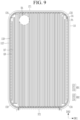
- connection structure of wiring positioned in the peripheral area of the display device and wiring positioned in the display area according to an embodiment will be further described with reference to FIGS. 9 to 11 .
- FIG. 9 is a schematic plan view illustrating some elements of a display device according to an embodiment
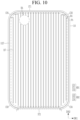
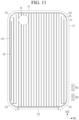
- FIGS. 10 and 11 are schematic plan views illustrating a part of FIG. 9
- FIG. 10 illustrates the first initialization voltage line and the wiring electrically connected thereto in the display device according to an embodiment
- FIG. 11 illustrates the second initialization voltage line and the wiring electrically connected thereto in the display device according to an embodiment
- FIG. 9 is a drawing illustrating FIGS. 10 and 11 together.
- the display device includes the first initialization voltage line 127 and the second initialization voltage line 128 positioned on the display area DA of the substrate 110. Also, the display device according to an embodiment further includes a first initialization voltage transmission line 1127 and a second initialization voltage transmission line 1128 positioned on the peripheral area PA of the substrate 110.
- the first initialization voltage transmission line 1127 can also be called as a first voltage transmission line 1127 and the second initialization voltage transmission line 1128 can also be called as a second voltage transmission line 1128.
- the display device may further include several wires such as the data line, the driving voltage line, the scan line, and the light emission control line in addition to the first initialization voltage line 127 and the second initialization voltage line 128, and the illustration of these wires is omitted from FIGS. 9 to 11 .
- a voltage transmission line for these wires may be further positioned on the peripheral area PA of the substrate 110.
- the display device may include first initialization voltage lines 127 (also called as first voltage lines 127), and the first initialization voltage lines 127 may extend in a direction parallel to each other.
- First initialization voltage lines 127 may extend in the second direction DR2.
- the first initialization voltage VINT1 may be applied to first initialization voltage lines 127.
- Each first voltage line 127 may have an individual length, in particular adapted to the shape of the corner parts.
- the display device may include second initialization voltage lines 128 (also called as second voltage lines 128), and the second initialization voltage lines 128 may extend in parallel to each other. Second initialization voltage lines 128 may extend in the second direction DR2. The second initialization voltage VINT2 may be applied to second initialization voltage lines 128. Each second voltage line 128 may have an individual length, in particular adapted to the shape of the corner parts.
- the first initialization voltage line 127 and the second initialization voltage line 128 may be alternately disposed.
- the second initialization voltage line 128 may be positioned on the left edge of the substrate 110, and the first initialization voltage line 127 may be positioned adjacent to the right side of the second initialization voltage line 128. Subsequently, the second initialization voltage line 128 and the first initialization voltage line 127 may be sequentially and repeatedly disposed.
- a hole area HA may be positioned within the display area DA.
- the hole area HA may be approximately circular, and may be positioned on the upper left side of the substrate 110. However, this is not an example, and the shape and position of the hole area HA may be variously changed.
- a camera, a proximity sensor, an illuminance sensor, a gesture sensor, a motion sensor, a fingerprint recognition sensor, and a biometric sensor may be positioned in the hole area HA.
- the first initialization voltage line 127 and the second initialization voltage line 128 may not be positioned in the hole area HA. In this case, the first initialization voltage line 127 positioned above the hole area HA and the first initialization voltage line 127 positioned below the hole area HA may not be electrically connected to each other. Similarly, the second initialization voltage line 128 positioned above the hole area HA and the second initialization voltage line 128 positioned below the hole area HA may not be electrically connected to each other.
- the first initialization voltage transmission line 1127 may have a shape surrounding the display area DA in a plan view.
- the first initialization voltage transmission line 1127 may have a closed ring shape to completely surround the display area DA in a plan view.
- the disclosure is not limited thereto, and the first initialization voltage transmission line 1127 may be electrically disconnected in at least some regions.
- the first initialization voltage transmission line 1127 may have an opened ring shape.
- the first initialization voltage transmission line 1127 may be electrically connected to first initialization voltage lines 127.
- the first initialization voltage transmission line 1127 and the first initialization voltage line 127 may be electrically connected at a first edge BD1 or a second edge BD2 of the substrate 110.
- the first edge BD1 and the second edge BD2 may face each other.
- the first edge BD1 may be an upper edge
- the second edge BD2 may be a lower edge.
- the substrate 110 may be approximately polygonal, and each corner of the polygon may have a rounded shape.
- the first edge BD1 may include a first corner part CO1, and a second corner part CO2 and a first straight-line part ST1 positioned between the first corner part CO1 and the second corner part CO2.
- the second edge BD2 may include a third corner part CO3, and a fourth corner part CO4 and a second straight-line part ST2 positioned between the third corner part CO3 and the fourth corner part CO4.
- the first initialization voltage transmission line 1127 and the first initialization voltage line 127 may be electrically connected to each other in the first corner part CO1, the second corner part CO2, and the first straight-line part ST1 of the first edge BD1. Also, the first initialization voltage transmission line 1127 and the first initialization voltage line 127 may be electrically connected to each other in the second straight-line part ST2 of the second edge BD2. The first initialization voltage transmission line 1127 and the first initialization voltage line 127 may not be electrically connected to each other, but may be separated from each other, at the third corner part CO3 and the fourth corner part CO4 of the second edge BD2.
- the second initialization voltage transmission line 1128 may have a shape surrounding the display area DA in a plan view.
- the second initialization voltage transmission line 1128 may have a closed ring shape to completely surround the display area DA in a plan view.
- the disclosure is not limited thereto, and the second initialization voltage transmission line 1128 may be electrically disconnected in at least some regions.
- the second initialization voltage transmission line 1128 may have an opened ring shape.
- the second initialization voltage transmission line 1128 may be positioned inside the first initialization voltage transmission line 1127.
- the second initialization voltage transmission line 1128 may be formed to surround the first initialization voltage transmission line 1127.
- the second initialization voltage transmission line 1128 may be electrically connected to second initialization voltage lines 128.
- the second initialization voltage transmission line 1128 and the second initialization voltage line 128 may be electrically connected to each other at the first edge BD1 or the second edge BD2 of the substrate 110.
- the second initialization voltage transmission line 1128 and the second initialization voltage line 128 may be electrically connected to each other in the third corner part CO3, the fourth corner part CO4, and the second straight-line part ST2 of the second edge BD2.
- the second initialization voltage transmission line 1128 and the second initialization voltage line 128 may be electrically connected to each other in the first straight-line part ST1 of the first edge BD1.
- the second initialization voltage transmission line 1128 and the second initialization voltage line 128 may not be electrically connected to each other, but may be separated from each other at the first corner part CO1 and the second corner part CO2 of the first edge BD1.
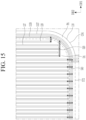
- connection structure of each wire in the first edge BD1 and the second edge BD2 will be further described with reference to FIGS. 12 to 15 .
- FIGS. 12 to 15 are schematic plan views illustrating some regions of a display device according to an embodiment.
- FIG. 12 illustrates the first corner part, the first straight-line part, and the surroundings thereof positioned on the upper left side of the display device according to an embodiment
- FIG. 13 illustrates the second corner part, the first straight-line part, and the surroundings thereof positioned on the upper right side of the display device according to an embodiment
- FIG. 14 illustrates the third corner part, the second straight-line part, and the surroundings thereof positioned on the lower left side of the display device according to an embodiment
- FIG. 15 illustrates the fourth corner part, the second straight-line part, and the surroundings thereof positioned on the lower right side of the display device according to an embodiment.
- a first bridge electrode 510, a second bridge electrode 520, a third bridge electrode 530, and a fourth bridge electrode 540 may be positioned between the display area DA and the peripheral area PA of the substrate 110.
- the first bridge electrode 510 and the second bridge electrode 520 may be positioned in the corner part and may be extended in the first direction DR1.
- the third bridge electrode 530 and the fourth bridge electrode 540 may be positioned in the straight-line part, and may be extended in the second direction DR2.
- the first initialization voltage transmission line 1127 and the first initialization voltage line 127 may be electrically connected to each other by the first bridge electrode 510.
- the first bridge electrode 510 may have a bar shape extending in the first direction DR1. A first end (or one end) of the first bridge electrode 510 may be electrically connected to the first initialization voltage transmission line 1127, and a second end (or another end) of the first bridge electrode 510 may be electrically connected to the first initialization voltage line 127.
- the first bridge electrode 510 may be electrically connected to a first initialization voltage line 127 or first initialization voltage lines 127.
- the first bridge electrode 510 may be electrically connected to two first initialization voltage lines 127.
- the first bridge electrode 510 may be positioned in the first corner part CO1 and the second corner part CO2 of the first edge BD1 of the substrate 110, and may not be positioned in the third corner part CO3 and the fourth corner part CO4 of the second edge BD2. Accordingly, the first initialization voltage transmission line 1127 and the first initialization voltage line 127 may not be electrically connected to each other, but may be separated in the third corner part CO3 and the fourth corner part CO4 of the second edge BD2.
- the second initialization voltage transmission line 1128 and the second initialization voltage line 128 may be electrically connected to each other by the second bridge electrode 520.
- the second bridge electrode 520 may have a bar shape extending in the first direction DR1. A first end of the second bridge electrode 520 may be electrically connected to the second initialization voltage transmission line 1128, and a second end of the second bridge electrode 520 may be electrically connected to the second initialization voltage line 128.
- the second bridge electrode 520 may be electrically connected to a second initialization voltage line 128 or second initialization voltage lines 128. For example, the second bridge electrode 520 may be electrically connected to two second initialization voltage lines 128.
- the number of the second initialization voltage lines 128 electrically connected to the second bridge electrode 520 may be variously changed.
- the second bridge electrode 520 may be positioned on the third corner part CO3 and the fourth corner part CO4 of the second edge BD2 of the substrate 110, and may not be positioned on the first corner part CO1 and the second corner part CO2 of the first edge BD1. Accordingly, the second initialization voltage transmission line 1128 and the second initialization voltage line 128 may not be electrically connected to each other, but may be separated from each other in the first corner part CO1 and the second corner part CO2 of the first edge BD1.
- the first initialization voltage transmission line 1127 and the first initialization voltage line 127 may be electrically connected to each other by the third bridge electrode 530.
- the third bridge electrode 530 may have a rod shape (or bar shape) extending in the second direction DR2. A first end of the third bridge electrode 530 may be electrically connected to the first initialization voltage transmission line 1127, and a second end of the third bridge electrode 530 may be electrically connected to the first initialization voltage line 127.
- the first initialization voltage transmission line 1127 and the first initialization voltage line 127 may be electrically connected to each other by the fourth bridge electrode 540.
- the fourth bridge electrode 540 may have a rod shape extending in the second direction DR2. A first end of the fourth bridge electrode 540 may be electrically connected to the first initialization voltage transmission line 1127, and a second end of the fourth bridge electrode 540 may be electrically connected to the first initialization voltage line 127.
- the second initialization voltage transmission line 1128 and the second initialization voltage line 128 may be directly connected to each other.
- the second initialization voltage transmission line 1128 and the second initialization voltage line 128 may be electrically connected to each other without using a separate bridge electrode.
- the connection structure between the wiring positioned in the display area DA and the wiring positioned in the peripheral area PA may be complicated.
- the first initialization voltage transmission line 1127 and the first initialization voltage line 127 are electrically connected to each other in only the first corner part CO1 and the second corner part CO2 of the first edge BD1, and are not electrically connected to each other in the third corner part CO3 and the fourth corner part CO4 of the second edge BD2.
- the display device according to an embodiment may have the connection structure of the wiring more advantageous than (e.g., more streamlined or simpler than) the structure in which the first initialization voltage transmission line 1127 and the first initialization voltage line 127 are electrically connected to each other in all corner parts.
- the second initialization voltage transmission line 1128 and the second initialization voltage line 128 are electrically connected to each other in only the third corner part CO3 and the fourth corner part CO4 of the second edge BD2, and are not electrically connected to each other in the first corner part CO1 and the second corner part CO2 of the first edge BD1.
- the display device according to an embodiment may have the wiring connection structure more advantageous than (e.g., more streamlined or simpler than) the structure in which the second initialization voltage transmission line 1128 and the second initialization voltage line 128 are electrically connected to each other in all corner parts. Accordingly, by simplifying the wiring connection structure in the display device according to an embodiment, the region where an image is not displayed may be reduced.
- the display device may show a simplified connection structure of the wiring compared to the structure in which the first initialization voltage transmission line 1127 and the first initialization voltage line 127 are connected in all corner parts.
- the first initialization voltage transmission line 1127 and the first initialization voltage line 127 are electrically connected to in the first straight-line part ST1 of the first edge BD1 and the second straight-line part ST2 of the second edge BD2.
- the first initialization voltage transmission line 1127 is electrically connected to ends of the first initialization voltage line 127, respectively, a drop in the voltage applied to the first initialization voltage line 127 may be prevented.
- the second initialization voltage transmission line 1128 and the second initialization voltage line 128 are electrically connected to each other in the first straight-line part ST1 of the first edge BD1 and the second straight-line part ST2 of the second edge BD2.
- the second initialization voltage transmission line 1128 is electrically connected to ends of the second initialization voltage line 128, respectively, a drop in the voltage applied to the second initialization voltage line 128 may be prevented.
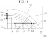
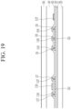
- each wire is further described further with reference to FIGS. 16 to 19 .
- FIG. 16 is a schematic enlarged plan view of a region of FIG. 13
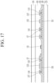
- FIG. 17 is a schematic cross-sectional view taken along line XVII-XVII' of FIG. 16
- FIG. 18 is a schematic enlarged plan view of a portion of FIG. 15
- FIG. 19 is a schematic cross-sectional view taken along line XIX-XIX' of FIG. 18 .
- a first bridge electrode 510, a second bridge electrode 520, a third bridge electrode 530, and a fourth bridge electrode 540 may be positioned on a substrate 110.
- the first to fourth bridge electrodes 510, 520, 530, and 540 may be positioned at a boundary between the display area DA and the peripheral area PA of the substrate 110.
- a part of the first to fourth bridge electrodes 510, 520, 530, and 540 may be positioned in the display area DA, and the remaining part may be positioned in the peripheral area PA.
- the first bridge electrode 510 and the second bridge electrode 520 may extend in the first direction DR1
- the third bridge electrode 530 and the fourth bridge electrode 540 may extend in the second direction DR2 perpendicular to the first direction DR1.
- the first to fourth bridge electrodes 510, 520, 530, and 540 and the gate conductor may be positioned on a same layer.
- a buffer layer 111 and a gate insulating layer 140 may be positioned between the substrate 110 and the first to fourth bridge electrodes 510, 520, 530, and 540.
- An interlayer insulating layer 160 may be positioned on the first to fourth bridge electrodes 510, 520, 530, and 540.
- One bridge electrode 510, 520 may be electrically connected to two first voltage lines 127.
- One bridge electrode 510, 520 may be electrically connected to two second voltage lines 128.
- Each bridge electrode 510 or bridge electrode 520 may have an individual length.
- one bridge electrode 510, 520 may be electrically connected to one first voltage lines 127 or one second voltage lines 128 and another bridge electrode 510, 520 may be electrically connected to two first voltage lines 127 or two second voltage lines 128. All the bridge electrodes 510, 520 may be additional electrically connected to a first or second initialization voltage transmission line 1127, 1128.
- the bridge electrode 510, 520 which may be electrically connected to two first voltage lines 127 or two second voltage lines 128 may have a greater length than the bridge electrode 510, 520 which may be electrically connected to only one first voltage lines 127 or one second voltage lines 128.
- a first initialization voltage line 127, a second initialization voltage line 128, a first initialization voltage transmission line 1127, and a second initialization voltage transmission line 1128 may be positioned on the interlayer insulating layer 160.
- the first initialization voltage line 127 and the second initialization voltage line 128 may be positioned on the display area DA of the substrate 110, and may extend in the second direction DR2.
- the first initialization voltage transmission line 1127 and the second initialization voltage transmission line 1128 may be positioned on the peripheral area PA of the substrate 110 and may have a shape surrounding the display area DA.
- the first initialization voltage line 127 may overlap the first bridge electrode 510.
- the interlayer insulating layer 160 may include an opening 1161 overlapping the first initialization voltage line 127 and the first bridge electrode 510.
- the first initialization voltage line 127 may be electrically connected to the first bridge electrode 510 through the opening 1161.
- the first initialization voltage transmission line 1127 may overlap the first bridge electrode 510.
- the interlayer insulating layer 160 may include an opening 1162 overlapping the first initialization voltage transmission line 1127 and the first bridge electrode 510.
- the first initialization voltage transmission line 1127 may be electrically connected to the first bridge electrode 510 through the opening 1162.
- the first initialization voltage line 127 and the first initialization voltage transmission line 1127 may be electrically connected to each other by the first bridge electrode 510.
- the first initialization voltage line 127 and the first initialization voltage transmission line 1127 may be electrically connected to each other by the first bridge electrode 510.
- the first initialization voltage line 127 may overlap the third bridge electrode 530.
- the interlayer insulating layer 160 may include an opening 1163 overlapping the first initialization voltage line 127 and the third bridge electrode 530.
- the first initialization voltage line 127 may be electrically connected to the third bridge electrode 530 through the opening 1163.
- the first initialization voltage transmission line 1127 may overlap the third bridge electrode 530.
- the interlayer insulating layer 160 may include an opening 1164 overlapping the first initialization voltage transmission line 1127 and the third bridge electrode 530.
- the first initialization voltage transmission line 1127 may be electrically connected to the third bridge electrode 530 through the opening 1164.
- the first initialization voltage line 127 and the first initialization voltage transmission line 1127 may be electrically connected to each other by the third bridge electrode 530.
- the first initialization voltage line 127 may overlap the fourth bridge electrode 540.
- the interlayer insulating layer 160 may include an opening 1167 overlapping the first initialization voltage line 127 and the fourth bridge electrode 540.
- the first initialization voltage line 127 may be electrically connected to the fourth bridge electrode 540 through the opening 1167.
- the first initialization voltage transmission line 1127 may overlap the fourth bridge electrode 540.
- the interlayer insulating layer 160 may include an opening 1168 overlapping the first initialization voltage transmission line 1127 and the fourth bridge electrode 540.
- the first initialization voltage transmission line 1127 may be electrically connected to the fourth bridge electrode 540 through the opening 1168.
- the first initialization voltage line 127 and the first initialization voltage transmission line 1127 on the second straight-line part ST2 of the substrate 110 may be electrically connected to each other by a fourth bridge electrode 540.
- the second initialization voltage line 128 on the third corner part CO3 of the substrate 110 may overlap the second bridge electrode 520.
- the interlayer insulating layer 160 may include an opening 1165 overlapping the second initialization voltage line 128 and the second bridge electrode 520.
- the second initialization voltage line 128 may be electrically connected to the second bridge electrode 520 through the opening 1165.
- the second initialization voltage transmission line 1128 may overlap the second bridge electrode 520.
- the interlayer insulating layer 160 may include an opening 1166 overlapping the second initialization voltage transmission line 1128 and the second bridge electrode 520.
- the second initialization voltage transmission line 1128 may be electrically connected to the second bridge electrode 520 through the opening 1166.
- the second initialization voltage transmission line 1128 and the second initialization voltage line 128 may be electrically connected to each other by the second bridge electrode 520.
- the second initialization voltage transmission line 1128 and the second initialization voltage line 128 may be electrically connected to each other by the second bridge electrode 520.
- a passivation layer 180 may be positioned on the first initialization voltage line 127, the second initialization voltage line 128, the first initialization voltage transmission line 1127, and the second initialization voltage transmission line 1128.
- a partition wall 350 may be positioned on the passivation layer 180.
- the first initialization voltage line 127 and the first initialization voltage transmission line 1127 are electrically connected to each other in the corner part of the first edge, and are not electrically connected to each other in the corner part of the second edge.
- the second initialization voltage line 128 and the second initialization voltage transmission 1128 line are electrically connected to each other in the corner part of the second edge, but are not electrically connected to each other in the corner part of the first edge.
- the display device according to an embodiment is not limited thereto, and the reverse may be possible.
- the first initialization voltage line and the first initialization voltage transmission line may be electrically connected to each other at the corner part of the second edge and not electrically connected to each other at the corner part of the first edge.
- the second initialization voltage line and the second initialization voltage transmission line may be electrically connected to each other at the corner part of the first edge and not electrically connected to each other at the corner part of the second edge.
- the second initialization voltage transmission line 1128 is positioned inside the first initialization voltage transmission line 1127, but the disclosure is not limited thereto.
- the second initialization voltage transmission line 1128 may be disposed in a border area of the peripheral area PA, which is near the display area DA, so that in particular the first initialization voltage transmission line 1127 may be the outermost line in the peripheral area PA.
- the first initialization voltage transmission line 1127 may be disposed neighbored to the second initialization voltage transmission line 1128 and far off the display area DA.
- the second initialization voltage transmission line may be positioned outside the first initialization voltage transmission line.
- the first initialization voltage transmission line may be positioned inside the second initialization voltage transmission line.
- the first initialization voltage transmission line 1127 may be disposed in a border area of the peripheral area PA, which is near the display area DA, so that in particular the second initialization voltage transmission line 1128 may be the outermost line in the peripheral area PA.
- the second initialization voltage transmission line 1128 may be disposed neighbored to the first initialization voltage transmission line 1127 and far off the display area DA.
- the second initialization voltage transmission line and the second initialization voltage line may be electrically connected to each other by a bridge electrode.
- the first initialization voltage transmission line and the first initialization voltage line may be directly connected to each other.
- connection structure of the first initialization voltage line and the first initialization voltage transmission line and the connection structure of the second initialization voltage line and the second initialization voltage transmission line have been described, but the disclosure is not limited thereto.
- the first initialization voltage line and the first initialization voltage transmission line to which the first initialization voltage is applied the first voltage line and the first voltage transmission line to which the first voltage is applied may be used.
- the second initialization voltage line and the second initialization voltage transmission line to which the second initialization voltage is applied the second voltage line and the second voltage transmission line to which the second voltage is applied may be used.
- the first voltage and the second voltage may each be a constant voltage.
- the first voltage may be different from the second voltage.
- the display device according to an embodiment is described with reference to FIG. 20 as follows.
- the display device according to the embodiment shown in FIG. 20 is substantially the same as the display device according to the embodiment shown in FIGS. 1 to 19 , so repetitive descriptions thereof are omitted.
- the connection relationship in the straight-line part of the substrate is different from the previous embodiment, and is further described below.
- FIG. 20 is a schematic plan view illustrating some elements of a display device according to an embodiment
- FIGS. 21 and 22 are schematic plan views illustrating some regions of a display device according to an embodiment.
- FIG. 21 illustrates the second corner part, the first straight-line part, and the surroundings thereof positioned on the upper right side of the display device according to an embodiment
- FIG. 22 illustrates the third corner part, the second straight-line part, and the surroundings thereof positioned on the lower left side of the display device according to an embodiment.
- the display device includes a first initialization voltage line 127 and a second initialization voltage line 128 positioned on the display area DA of the substrate 110.
- the display device further includes a first initialization voltage transmission line 1127 and a second initialization voltage transmission line 1128 positioned on the peripheral area PA of the substrate 110.
- First initialization voltage lines 127 and second initialization voltage lines 128 may extend in the second direction DR2.
- the first initialization voltage VINT1 may be applied to first initialization voltage lines 127.
- the second initialization voltage VINT2 may be applied to second initialization voltage lines 128.
- the first initialization voltage transmission line 1127 may have a shape surrounding the display area DA in a plan view. In this case, the first initialization voltage transmission line 1127 may be positioned adjacent to the left edge, the upper edge, and the right edge of the display area DA in a plan view, and may not be positioned adjacent to the lower edge thereof.
- the first initialization voltage transmission line 1127 may be electrically connected to first initialization voltage lines 127.
- the first initialization voltage transmission line 1127 and the first initialization voltage line 127 may be electrically connected to each other at the first edge BD1 of the substrate 110.
- the first edge BD1 may be an upper edge.
- the first initialization voltage transmission line 1127 and the first initialization voltage line 127 may be electrically connected to each other in the first corner part CO1, the second corner part CO2, and the first straight-line part ST1 of the first edge BD1.
- the first initialization voltage transmission line 1127 and the first initialization voltage line 127 may not be electrically connected to each other, but may be separated from each other, in the third corner part CO3, the fourth corner part CO4, and the second straight-line part ST2 of the second edge BD2.
- the first initialization voltage transmission line 1127 and the first initialization voltage line 127 may be electrically connected to each other by the first bridge electrode 510.
- the first bridge electrode 510 may have a bar shape extending in the first direction DR1. A first end (or one end) of the first bridge electrode 510 may be electrically connected to the first initialization voltage transmission line 1127, and a second end (or anther end) of the first bridge electrode 510 may be electrically connected to the first initialization voltage line 127.
- the first initialization voltage transmission line 1127 and the first initialization voltage line 127 may be electrically connected to each other by the third bridge electrode 530.
- the third bridge electrode 530 may have a rod shape extending in the second direction DR2. A first end of the third bridge electrode 530 may be electrically connected to the first initialization voltage transmission line 1127, and a second end of the third bridge electrode 530 may be electrically connected to the first initialization voltage line 127.
- the first initialization voltage transmission line 1127 and the first initialization voltage line 127 may not be electrically connected to each other.
- the first initialization voltage transmission line 1127 may not be positioned in the second straight-line part ST2 of the second edge BD2 of the substrate 110.
- the second initialization voltage transmission line 1128 may have a shape surrounding the display area DA in a plan view.
- the second initialization voltage transmission line 1128 may have a closed ring shape to completely surround the display area DA in a plan view.
- the disclosure is not limited thereto, and the second initialization voltage transmission line 1128 may be electrically disconnected in at least some regions.
- the second initialization voltage transmission line 1128 may be positioned adjacent to the left edge, the lower edge, and the right edge of the display area DA in a plan view, and may not be positioned adjacent to the upper edge thereof.
- the second initialization voltage transmission line 1128 may be electrically connected to second initialization voltage lines 128.
- the second initialization voltage transmission line 1128 and the second initialization voltage line 128 may be electrically connected to each other at the second edge BD2 of the substrate 110.
- the second edge BD2 may be the lower edge.
- the second initialization voltage transmission line 1128 and the second initialization voltage line 128 may be electrically connected to each other in the third corner part CO3, the fourth corner part CO4, and the second straight-line part ST2 of the second edge BD2.
- the second initialization voltage transmission line 1128 and the second initialization voltage line 128 may not be electrically connected to each other and may be separated from each other, in the first corner part CO1, the second corner part CO2, and the first straight-line part ST1 of the first edge BD1.
- the second initialization voltage transmission line 1128 and the second initialization voltage line 128 may be electrically connected to each other by a second bridge electrode 520.
- the second bridge electrode 520 may have a bar shape extending in the first direction DR1. A first end of the second bridge electrode 520 may be electrically connected to the second initialization voltage transmission line 1128, and a second end of the second bridge electrode 520 may be electrically connected to the second initialization voltage line 128.
- the second initialization voltage transmission line 1128 and the second initialization voltage line 128 may be directly connected to each other.
- the second initialization voltage transmission line 1128 and the second initialization voltage line 128 may be electrically connected to each other without using a separate bridge electrode.
- the second initialization voltage transmission line 1128 and the second initialization voltage line 128 may not be electrically connected to each other.
- FIG. 21 illustrates that the second initialization voltage transmission line 1128 is positioned in the first straight-line part ST1 of the first edge BD1 of the substrate 110, the disclosure is not limited thereto, and the second initialization voltage transmission line 1128 may not be positioned in the first straight-line part ST1 of the substrate 110.
- the first initialization voltage transmission line 1127 and the first initialization voltage line 127 are electrically connected to each other in only the first corner part CO1, the second corner part CO2, and the first straight-line part ST1 of the first edge BD1, and are not electrically connected to each other in the third corner part CO3, the fourth corner part CO4, and the second straight-line part ST2 of the second edge BD2.
- the display device according to an embodiment may have the connection structure of the wiring more advantageous than (e.g., more streamlined or simpler than) the structure in which the first initialization voltage transmission line 1127 and the first initialization voltage line 127 are electrically connected to each other at both edges, and it is possible to reduce the region where an image is displayed. Also, it is possible to prevent a voltage difference between the wiring electrically connected to the corner part and the wiring electrically connected to the straight-line part.
- the second initialization voltage transmission line 1128 and the second initialization voltage line 128 are electrically connected to each other only in the third corner part CO3, the fourth corner part CO4, and the second straight-line part ST2 of the second edge BD2, and are not electrically connected to each other in the first corner part CO1, the second corner part CO2, and the first straight-line part ST1 of the first edge BD1.
- the display device according to an embodiment may have the connection structure of the wiring more advantageous than (e.g., more streamlined or simpler than) the structure in which the second initialization voltage transmission line 1128 and the second initialization voltage line 128 are electrically connected to each other at both edges, and the region where an image is not displayed may be reduced. Also, it is possible to prevent a voltage difference between the wiring electrically connected to the corner part and the wiring electrically connected to the straight-line part.
- the first initialization voltage line and the first initialization voltage transmission line are electrically connected to each other at the first edge and not electrically connected to each other at the second edge.
- the second initialization voltage line and the second initialization voltage transmission line are electrically connected to each other at the second edge and not electrically connected to each other at the first edge.
- the display device according to an embodiment is not limited thereto, and vice versa may be possible.
- the first initialization voltage line and the first initialization voltage transmission line may be electrically connected to each other at the second edge and not electrically connected to each other at the first edge.
- the second initialization voltage line and the second initialization voltage transmission line may be electrically connected to each other at the first edge and not electrically connected to each other at the second edge.
- the second initialization voltage transmission line is positioned inside the first initialization voltage transmission line, but conversely, the second initialization voltage transmission line may be positioned outside the first initialization voltage transmission line.
- connection structure of the first initialization voltage line and the first initialization voltage transmission line and the connection structure of the second initialization voltage line and the second initialization voltage transmission line have been described in the embodiment, it is not limited thereto, and may also be applied to the connection structure of the wires to which a different voltage is applied instead of the initialization voltage.
Landscapes
- Engineering & Computer Science (AREA)
- Microelectronics & Electronic Packaging (AREA)
- Physics & Mathematics (AREA)
- Geometry (AREA)
- Devices For Indicating Variable Information By Combining Individual Elements (AREA)
- Electroluminescent Light Sources (AREA)
Abstract
Description
- The present invention relates to a display device.
- A display device is a device that displays a screen, and includes a liquid crystal display (LCD), an organic light emitting diode (OLED), and the like. The display device is used in various electronic devices such as a mobile phone, a navigation device, a digital camera, an electronic book, a portable game machine, and various terminals.
- An organic light emitting diode (OLED) display includes two electrodes and an organic emission layer interposed therebetween. Electrons injected from one electrode and holes injected from another electrode are combined in the organic emission layer to generate excitons. The generated excitons are changed to a ground state from an exited state, releasing energy to emit light.
- The organic light emitting diode display includes pixels including an organic light emitting diode as a self-emissive element, and transistors for driving the organic light emitting diode and at least one capacitor are formed in each pixel. In addition, the organic light emitting device may further include a voltage line to which a signal for driving pixels is applied, and a voltage transmission line for transmitting a signal to the voltage line. These voltage lines and voltage transmission lines may be connected at the edge of the display device, and in case that the connection structure is complicated, the region where the screen is not displayed (also called "a dead space") may become larger.
- The above information disclosed in this Background section is only for enhancement of understanding of the background of the described technology, and therefore it may contain information that does not form the prior art that is already known in this country to a person of ordinary skill in the art.
- The present invention provides a display device according to the independent claim. The dependent claims describe preferred embodiments. Embodiments are to provide a display device capable of reducing a region in which an image is not displayed.
- The display device according to the invention includes a substrate including a display area and a peripheral area; a first voltage line disposed on the display area of the substrate, a first voltage being applied to the first voltage line; a second voltage line disposed on the display area of the substrate and extending in a direction parallel to the first voltage line, a second voltage being applied to the second voltage line; a first voltage transmission line disposed on the peripheral area of the substrate and transmitting the first voltage; a second voltage transmission line disposed on the peripheral area of the substrate and transmitting the second voltage; a first bridge electrode disposed on the first edge of the substrate and connecting the first voltage line and the first voltage transmission line; and a second bridge electrode disposed on the second edge of the substrate and connecting the second voltage line and the second voltage transmission line.
- The first edge and the second edge may face each other.
- The first voltage and the second voltage may be constant, and the first voltage may be different from the second voltage.
- The substrate may have a polygonal shape. The substrate may have corner parts. Each corner part of the substrate may have a rounded shape, and the first bridge electrode and the second bridge electrode may be disposed at the each corner part.
- The first bridge electrode and the second bridge electrode may extend in a first direction, and the first voltage line, and the second voltage line may extend in a second direction perpendicular to the first direction.
- The first edge of the substrate may include a first corner part, a second corner part (these corner parts may be the same corner parts as described above), and a first straight-line part disposed between the first corner part and the second corner part; the second edge of the substrate may include a third corner part, a fourth corner part, and a second straight-line part disposed between the third corner part and the fourth corner part; the first bridge electrode may be disposed on the first corner part and the second corner part, and is not disposed on the third corner part and the fourth corner part; and the second bridge electrode may be disposed on the third corner part and the fourth corner part, and is not disposed on the first corner part and the second corner part.
- The first voltage line and the first voltage transmission line may be electrically connected over the first corner part and the second corner part, and may be electrically disconnected over the third corner part and the fourth corner part, and the second voltage line and the second voltage transmission line may be electrically connected over the third corner part and the fourth corner part, and may be electrically disconnected over the first corner part and the second corner part.
- The display device according to an embodiment may further include a third bridge electrode disposed on the first straight-line part of the first edge of the substrate and electrically connecting the first voltage line and the first voltage transmission line; and a fourth bridge electrode disposed on the second straight-line part of the second edge of the substrate and electrically connecting the first voltage line and the first voltage transmission line. The third bridge electrode and the fourth bridge electrode may extend in the second direction, the first voltage transmission line and the second voltage transmission line may have a shape surrounding the display area in a plan view, and the first voltage transmission line may be disposed outside the second voltage transmission line.
- The second voltage line and the second voltage transmission line may be directly connected on the first straight-line part and the second straight-line part.
- The display device according to an embodiment may further include a third bridge electrode disposed on the first straight-line part of the first edge of the substrate and electrically connecting the first voltage line and the first voltage transmission line, the third bridge electrode may extend in the second direction, the first voltage line and the first voltage transmission line may be electrically disconnected on the second straight-line part of the second edge of the substrate, the first voltage transmission line and the second voltage transmission line may have a shape surrounding the display area in a plan view, and the first voltage transmission line may be disposed outside the second voltage transmission line.
- The second voltage line and the second voltage transmission line may be directly connected on the second straight-line part, and electrically disconnected on the first straight-line part.
- The display device according to an embodiment may further include a semiconductor layer disposed on the substrate and including a channel, a first region and a second region of a first transistor, a channel of a first region and a second region of a second transistor, and a channel, a first region, and a second region of a third transistor; a gate conductor including a gate electrode of the first transistor overlapping the channel of the first transistor in a plan view, a gate electrode of the second transistor overlapping the channel of the second transistor in a plan view, and a gate electrode of the seventh transistor overlapping the channel of the third transistor in a plan view; and a data conductor including a connection electrode electrically connecting a gate electrode of the first transistor and a second region of the second transistor.
- The first voltage line may be electrically connected to the first region of the second transistor, and the first voltage may be a first initialization voltage.
- The first voltage line and the data conductor may be disposed on a same layer.
- The first voltage transmission line and the data conductor may be disposed on a same layer.
- The second voltage line may be electrically connected to the second region of the third transistor, and the second voltage may be a second initialization voltage.
- The second voltage line and the data conductor may be disposed on a same layer.
- The second voltage transmission line and the data conductor may be disposed on a same layer.
- The first bridge electrode, the second bridge electrode, and the gate conductor may be disposed on a same layer.
- The display device according to an embodiment may further include a data line and a driving voltage line extending in a direction parallel to the first voltage line and the second voltage line, and the data line, the driving voltage line, and the data conductor may be disposed on a same layer.
- The data line and the driving voltage line may be disposed between the first voltage line and the second voltage line in a plan view.
- The display device may include pixels, each the pixels may include the first transistor, the second transistor, and the third transistor, and the pixels may have a symmetrical shape with respect to the second voltage line.
- According to embodiments, the region where an image is not displayed may be reduced in the display device.
- The above and other aspects, features, and advantages of certain embodiments of the disclosure will be more apparent from the following description taken in conjunction with the accompanying drawings, in which:
-
FIG. 1 is a schematic plan view of a display device according to an embodiment. -
FIG. 2 is a schematic diagram of an equivalent circuit of a pixel of a display device according to an embodiment. -
FIG. 3 is a schematic plan view showing a part of a display device according to an embodiment. -
FIG. 4 is a schematic cross-sectional view of a display device according to an embodiment taken along line IV-IV' ofFIG. 3 . -
FIG. 5 is a schematic cross-sectional view of a display device according to an embodiment taken along line V-V' ofFIG. 3 . -
FIG. 6 to FIG. 8 are schematic plan views sequentially showing a display device according to an embodiment according to a manufacturing order. -
FIG. 9 is a schematic plan view showing some constituent elements of a display device according to an embodiment. -
FIG. 10 andFIG. 11 are schematic plan views showing a part ofFIG. 9 . -
FIG. 12 to FIG. 15 are schematic plan views showing some region of a display device according to an embodiment. -
FIG. 16 is a schematic enlarged plan view of some region ofFIG. 13 . -
FIG. 17 is a schematic cross-sectional view taken along line XVII-XVII' ofFIG. 16 . -
FIG. 18 is a schematic enlarged plan view of some region ofFIG. 15 . -
FIG. 19 is a schematic cross-sectional view taken along line XIX-XIX' ofFIG. 18 . -
FIG. 20 is a schematic plan view showing some constituent elements of a display device according to an embodiment. -
FIG. 21 andFIG. 22 are schematic plan views showing some region of a display device according to an embodiment. - The disclosure will be described more fully hereinafter with reference to the accompanying drawings, in which embodiments of the disclosure are shown. As those skilled in the art would realize, the described embodiments may be modified in various different ways, all without departing from the scope of the disclosure.
- Descriptions of parts not related to the disclosure are omitted, and like reference numerals designate like elements throughout the specification.
- Further, since sizes and thicknesses of elements shown in the accompanying drawings are arbitrarily given for better understanding and ease of description, the disclosure is not limited to the illustrated sizes and thicknesses. In the drawings, the thickness of layers, films, panels, regions, etc., may be exaggerated for clarity. In the drawings, for better understanding and ease of description, the thicknesses of some layers and areas may be exaggerated.
- It will be understood that when an element such as a layer, film, region, or substrate is referred to as being "on" another element, it can be directly on the other element or intervening elements may also be present. In contrast, when an element is referred to as being "directly on" another element, there are no intervening elements present. Further, in the specification, the word "on" or "above" means disposed or positioned on or below the object portion, and does not necessarily mean positioned on the upper side of the object portion based on a gravitational direction.
- In addition, unless explicitly described to the contrary, the word "comprise", and variations such as "comprises" or "comprising", will be understood to imply the inclusion of stated elements but not the exclusion of any other elements.
- Further, throughout the specification, the phrase "on a plane" or "in a plan view" means viewing a target portion from the top, and the phrase "on a cross-section" means viewing a cross-section formed by vertically cutting a target portion from the side.
- The phrase "at least one of" is intended to include the meaning of "at least one selected from the group of" for the purpose of its meaning and interpretation. For example, "at least one of A and B" may be understood to mean "A, B, or A and B."
- Unless otherwise defined or implied herein, all terms (including technical and scientific terms) used herein have the same meaning as commonly understood by those skilled in the art to which this disclosure pertains. It will be further understood that terms, such as those defined in commonly used dictionaries, should be interpreted as having a meaning that is consistent with their meaning in the context of the relevant art and the disclosure, and should not be interpreted in an ideal or excessively formal sense unless clearly so defined herein.
- First, a display device according to an embodiment is described with reference to
FIG. 1 . -
FIG. 1 is a schematic plan view showing a display device according to an embodiment. - As shown in
FIG. 1 , adisplay device 1000 according to an embodiment includes asubstrate 110 and pixels PX positioned on (or disposed on) thesubstrate 110. - The
substrate 110 may include a first region A1, a second region A2, and a bending region BA positioned between the first region A1 and the second region A2. Thesubstrate 110 may be made of a flexible material and may be changed into various shapes. Thesubstrate 110 may be flexible, stretchable, foldable, bendable, or rollable. The bending region BA may be a region in which thesubstrate 110 is bent. The first region A1 and the second region A2 may have a flat shape. However, this is only an example, and thesubstrate 110 may additionally include a region to be bent. For example, at least a portion of the first region A1 or the second region A2 of thesubstrate 110 may be bent. - The first region A1 of the
substrate 110 extends from the bending region BA. The first region A1 may be approximately formed as a rectangle including a long side and a short side, and a corner portion may be chamfered to have a rounded shape. However, the shape of the first region A1 is only an example and may be changed to various shapes. The first region A1 may include a display area DA and a peripheral area PA. The display area DA may be positioned in the center of the first region A1, and may have a shape approximately similar to that of the first region A1. The peripheral area PA may surround the display area DA. For example, the peripheral area PA may be positioned outside the first region A1. - Pixels PX may be positioned in the display area DA. Pixels PX may be disposed in a matrix form, and may receive an image signal and display an image accordingly. In this case, the arrangement shape of pixels PX may be variously changed. Although not shown in the drawings, the display device according to an embodiment may further include signal lines. The signal lines may include scan lines, light emission control lines, data lines, first initialization voltage lines (also called as first voltage lines), second initialization voltage lines (also called as second voltage lines), driving voltage lines, and the like. Theses signal lines may transmit a scan signal, a light emission control signal, a data signal, a first initialization voltage, a second initialization voltage, a driving voltage, and the like. Signal lines may be positioned to intersect each other in the first direction DR1 or the second direction DR2. In this case, the first direction DR1 may be a row direction, and the second direction DR2 may be a column direction. Also, each pixel PX may include transistors, a capacitor, and at least one light-emitting diode (LED), which are electrically connected to signal lines. For example, the display device according to an embodiment may be an organic light emitting device. However, the type of display device is not limited thereto, and various types of the display devices may be used. For example, the display device may be formed as a liquid crystal display, an electrophoretic display, or an electrowetting display device. In addition, the display device may be a next-generation display device such as a micro light emitting diode (Micro LED) display device, a quantum dot light-emitting diode (QLED) display device, and a quantum dot organic light-emitting diode (QD-OLED) display device.
- A voltage transmission line for transmitting a voltage to signal lines may be positioned in the peripheral area PA. In this case, the voltage transmission line may be formed to surround the display area DA. The voltage transmission line may include a first initialization voltage transmission line (also called as first voltage transmission line), a second initialization voltage transmission line (also called as second voltage transmission line), and the like. The first initialization voltage transmission line may be electrically connected to the first initialization voltage line to transmit the first initialization voltage. The second initialization voltage transmission line may be electrically connected to the second initialization voltage line to transmit the second initialization voltage.
- The second region A2 of the
substrate 110 extends from the bending region BA. The second region A2 is a non-display area that does not display an image and does not include pixels PX. Elements and/or wires for generating and/or transmitting various signals applied to the pixel PX are located in the second region A2. - A driving
circuit chip 250 and aflexible circuit board 200 may be positioned on the second region A2. The drivingcircuit chip 250 is electrically connected to the elements or wires positioned in the second region A2 to transmit various signals to pixels PX. For example, the drivingcircuit chip 250 may supply a scan signal, a control signal, a data signal, and the like. Theflexible circuit board 200 may be attached to the edge of the second region A2 of thesubstrate 110. Theflexible circuit board 200 may be made of a flexible material. Theflexible circuit board 200 has a circuit designed to control the operation of the display device. - The bending region BA of the
substrate 110 may be positioned between the first region A1 and the second region A2 to electrically connect the first region A1 to the second region A2. In case that thesubstrate 110 is bent, the first region A1 and the second region A2 may overlap each other. The bending region BA of thesubstrate 110 may be positioned so that it is connected (or extended) to a short side of the first region A1. However, the position of the bending region BA is only an example and may be variously changed. For example, the bending region BA may be positioned so that it is connected to short sides of the first region A1, or it may be positioned so that it is connected to a long side of the first region A1. - Hereinafter, a pixel of the display device according to an embodiment is described with reference to
FIG. 2 . -
FIG. 2 is a schematic diagram of an equivalent circuit of a pixel of a display device according to an embodiment. - As shown in
FIG. 2 , the display device according to an embodiment includes pixels PX capable of displaying an image andsignal lines signal lines - The signal lines 127, 128,151,152,154,155,171, and 172 may include a first initialization voltage line (or first voltage line) 127, a second initialization voltage line (or second voltage line) 128,
scan lines emission control line 155, adata line 171, and a drivingvoltage line 172. - The first
initialization voltage line 127 may transmit a first initialization voltage VINT1, and the secondinitialization voltage line 128 may transmit a second initialization voltage VINT2. Thescan lines - The
scan lines first scan line 151 capable of transmitting a scan signal GWn, asecond scan line 152 capable of transmitting a scan signal GIn having a gate-on voltage at different timing from that of thefirst scan line 151, and athird scan line 154 capable of transmitting a scan signal GI(n+1). In the embodiment, an example in which thesecond scan line 152 transmits the gate-on voltage at earlier timing than thefirst scan line 151 is described. For example, in case that the scan signal GWn is an n-th scan signal Sn among scan signals applied during a frame (where n is a natural number of 1 or more), the scan signal GIn may be a previous scan signal such as an (n-1)-th scan signal S(n-1), and the scan signal GI(n+1) may be an n-th scan signal Sn. However, the embodiment is not limited thereto, and the scan signal GI(n+1) may be a different scan signal from the n-th scan signal Sn. - The light
emission control line 155 may transmit a control signal, and particularly may transmit a light emission control signal EM capable of controlling emission of the light-emitting diode LED included in the pixel PX. The control signal transmitted by the lightemission control line 155 may consist of a gate-on voltage and a gate-off voltage, and may have a different waveform from the scan signal transmitted by thescan lines - The
data line 171 may transmit a data signal Dm, and the drivingvoltage line 172 may transmit a driving voltage ELVDD. The data signal Dm may have other voltage levels according to the image signal input to the display device, and the driving voltage ELVDD may have a substantially constant level. - Although not shown in the drawings, the display device may further include a driver for transmitting signals to signal lines 127,151, 152, 154, 155, 171, and 172.
- Transistors T1, T2, T3, T4, T5, T6, and T7 included in a pixel PX include a first transistor T1, a second transistor T2, a third transistor T3, a fourth transistor T4, a fifth transistor T5, a sixth transistor T6, and a seventh transistor T7.
- The
first scan line 151 may transmit the scan signal GWn to the second transistor T2 and the third transistor T3, thesecond scan line 152 may transmit the scan signal GIn to the fourth transistor T4, thethird scan line 154 may transmit the scan signal GI(n+1) to the seventh transistor T7, and the lightemission control line 155 may transmit the light emission control signal EM to the fifth transistor T5 and the sixth transistor T6. - A gate electrode G1 of the first transistor T1 is electrically connected to a first terminal of the capacitor Cst through a driving gate node GN, a first electrode Ea1 of the first transistor T1 is electrically connected to the driving
voltage line 172 via the fifth transistor T5, and a second electrode Eb1 of the first transistor T1 is electrically connected to an anode of the light-emitting diode LED via the sixth transistor T6. The first transistor T1 may receive the data signal Dm transmitted by thedata line 171 depending on the switching operation of the second transistor T2 to supply a driving current Id to the light-emitting diode LED. - A gate electrode G2 of the second transistor T2 is electrically connected to the
first scan line 151, a first electrode Ea2 of the second transistor T2 is electrically connected to thedata line 171, and a second electrode Eb2 of the second transistor T2 is electrically connected to the first electrode Ea1 of the first transistor T1 and is electrically connected to the drivingvoltage line 172 via the fifth transistor T5. The second transistor T2 is turned on depending on the scan signal GWn transmitted through thefirst scan line 151, thereby transmitting the data signal Dm, transmitted from thedata line 171, to the first electrode Ea1 of the first transistor T1. - A gate electrode G3 of the third transistor T3 is electrically connected to the
first scan line 151, and a first electrode Ea3 of the third transistor T3 is electrically connected to the second electrode Eb1 of the first transistor T1 and is electrically connected to the anode of the light-emitting diode LED via the sixth transistor T6. A second electrode Eb3 of the third transistor T3 is electrically connected to a second electrode Eb4 of the fourth transistor T4, the first terminal of the capacitor Cst, and the gate electrode G1 of the first transistor T1. The third transistor T3 is turned on depending on the scan signal GWn transmitted through thefirst scan line 151 to electrically connect the gate electrode G1 and the second electrode Eb1 of the first transistor T1 to each other, thereby electrically diode-connecting the first transistor T1. - A gate electrode G4 of the fourth transistor T4 is electrically connected to the
second scan line 152, a first electrode Ea4 of the fourth transistor T4 is electrically connected to the firstinitialization voltage line 127, and the second electrode Eb4 of the fourth transistor T4 is electrically connected to the first terminal of the capacitor Cst and the gate electrode G1 of the first transistor T1 through the second electrode Eb3 of the third transistor T3. The fourth transistor T4 is turned on depending on the scan signal GIn transmitted through thesecond scan line 152 to transmit the first initialization voltage VINT1 to the gate electrode G1 of the first transistor T1, thereby performing an initialization operation of initializing the voltage of the gate electrode G1 of the first transistor T1. - A gate electrode G5 of the fifth transistor T5 is electrically connected to the light
emission control line 155, a first electrode Ea5 of the fifth transistor T5 is electrically connected to the drivingvoltage line 172, and a second electrode Eb5 of the fifth transistor T5 is electrically connected to the first electrode Ea1 of the first transistor T1 and the second electrode Eb2 of the second transistor T2. - A gate electrode G6 of the sixth transistor T6 is electrically connected to the light
emission control line 155, a first electrode Ea6 of the sixth transistor T6 is electrically connected to the second electrode Eb1 of the first transistor T1 and the first electrode Ea3 of the third transistor T3, and a second electrode Eb6 of the sixth transistor T6 is electrically connected to the anode of the light-emitting diode LED. The fifth transistor T5 and the sixth transistor T6 are simultaneously turned on depending on the light emission control signal EM transmitted through the lightemission control line 155, thereby transmitting the driving voltage ELVDD to the light-emitting diode LED through the diode-connected first transistor T1. - A gate electrode G7 of the seventh transistor T7 is electrically connected to the
third scan line 154, a first electrode Ea7 of the seventh transistor T7 is electrically connected to the second electrode Eb6 of the sixth transistor T6 and the anode of the light-emitting diode LED, and a second electrode Eb7 of the seventh transistor T7 is electrically connected to the secondinitialization voltage line 128. The seventh transistor T7 is turned on according to the scan signal GI(n+1) received through thethird scan line 154 and transmits the second initialization voltage VINT2 to the anode of the light-emitting diode LED, thereby serving to initialize the anode of the light-emitting diode LED. In the embodiment, different initialization voltages may be applied to the fourth transistor T4 and the seventh transistor T7. For example, the first initialization voltage VINT1 may be applied to the fourth transistor T4, and the second initialization voltage VINT2 may be applied to the seventh transistor T7. Therefore, it is possible to improve the characteristic of the display device according to an embodiment. - The transistors T1, T2, T3, T4, T5, T6, and T7 may be P-type channel transistors such as a P-channel metal oxide semiconductor (PMOS), but are not limited thereto, and at least one among the transistors T1, T2, T3, T4, T5, T6, and T7 may be an N-type channel transistor and may include both a P-type and an N-type channel transistor.
- The first terminal of the capacitor Cst is electrically connected to the gate electrode G1 of the first transistor T1 as described above and a second terminal is electrically connected to the driving
voltage line 172. The cathode of the light-emitting diode LED is electrically connected to a common voltage ELVSS terminal that transmits a common voltage ELVSS, so that the common voltage ELVSS may be applied thereto. - The structure of the pixel PX according to an embodiment is not limited to the structure shown in
FIG. 2 , and the number of transistors and the number of capacitors included in a pixel PX and the connection relationship therebetween may be variously modified. - Hereinafter, the interlayer structure of a pixel of the display device according to an embodiment will be further described with reference to
FIGS. 3 to 8 . -
FIG. 3 is a schematic plan view illustrating a part of a display device according to an embodiment,FIG. 4 is a schematic cross-sectional view of a display device according to an embodiment taken along line IV-IV' ofFIG. 3 , andFIG. 5 is a schematic cross-sectional view of a display device according to an embodiment taken along line V-V' ofFIG. 3 .FIGS. 6 to 8 are schematic plan views sequentially illustrating a display device according to an embodiment an according to a manufacturing order.FIGS. 3 to 8 illustrate two adjacent pixels positioned in the display area of a display device according to an embodiment. In this case, two adjacent pixels may have planar structures that are symmetrical to each other. However, the disclosure is not limited thereto, and two adjacent pixels may have a same planar structure. - As shown in
FIGS. 3 to 8 , the display device according to an embodiment may include asubstrate 110. Thesubstrate 110 may include at least one among polystyrene, polyvinyl alcohol, polymethyl methacrylate, polyethersulfone, polyacrylate, polyetherimide, polyethylene naphthalate, polyethylene terephthalate, polyphenylene sulfide, polyarylate, polyimide, polycarbonate, cellulose triacetate, and cellulose acetate propionate. Thesubstrate 110 may be single-layered or multi-layered. Thesubstrate 110 may have a structure in which at least one base layer and at least one inorganic layer, including a polymer resin sequentially stacked, are alternately stacked. - A semiconductor layer including a
channel 1132, afirst region 1131, and asecond region 1133 of the first transistor T1 may be positioned on thesubstrate 110.FIG. 6 illustrates a semiconductor layer. The semiconductor layer may further include achannel 4132, afirst region 4131, and asecond region 4133 of the fourth transistor T4, and achannel 7132, afirst region 7131, and asecond region 7133 of the seventh transistor T7 as well as the first transistor T1. In addition, the semiconductor layer may further include a channel, a first region, and a second region of each of the second transistor T2, the third transistor T3, the fifth transistor T5, and the sixth transistor T6. - The
channel 1132 of the first transistor T1 may have a U shape in a plan view. Thechannel 1132 may have a U shape in the length of the channel, this may be a U shape in a plane defined by the directions DR1 and DR2. However, the shape of thechannel 1132 of the first transistor T1 is not limited thereto, and may be variously changed. For example, thechannel 1132 of the first transistor T1 may be bent into a different shape or may be formed into a bar shape. Thefirst region 1131 and thesecond region 1133 of the first transistor T1 may be positioned on respective sides of thechannel 1132 of the first transistor T1. Thefirst region 1131 of the first transistor T1 may extend up and down in a plan view, so that a portion thereof extending downward may be electrically connected to the second region of the fifth transistor T5, and a portion thereof extending upward may be electrically connected to the second region of the second transistor T2. Thesecond region 1133 of the first transistor T1 may extend up and down in a plan view, so that a portion thereof extending downward may be electrically connected to the first region of the sixth transistor T6, and a portion thereof extending upward may be electrically connected to the first region of the third transistor T3. - The fourth transistor T4 may include two
channels 4132, thefirst region 4131 may be positioned on a side of achannel 4132, and thesecond region 4133 may be positioned on a side of theother channel 4132. Thesecond region 4133 of the fourth transistor T4 may extend downward in a plan view to be electrically connected to the second region of the third transistor T3. - The
first region 7131 and thesecond region 7133 of the seventh transistor T7 may be positioned on respective sides of thechannel 7132 of the seventh transistor T7. Thefirst region 7131 of the seventh transistor T7 may extend upward in a plan view to be electrically connected to the second region of the sixth transistor T6. - A
buffer layer 111 may be positioned between thesubstrate 110, and the semiconductor layer including thechannel 1132, thefirst region 1131, and thesecond region 1133 of the first transistor T1, thechannel 4132, thefirst region 4131, and thesecond region 4133 of the fourth transistor T4, and thechannel 7132, thefirst region 7131, and thesecond region 7133 of the seventh transistor T7. Thebuffer layer 111 may have a single-layer or a multi-layered structure. Thebuffer layer 111 may include an inorganic insulating material or an organic insulating material such as a silicon nitride (SiNx), a silicon oxide (SiOx), or a silicon oxynitride (SiOxNy). In addition, a barrier layer may be further positioned between thesubstrate 110 and thebuffer layer 111. The barrier layer may have a single-layer or a multi-layered structure. The barrier layer may include an inorganic insulating material such as a silicon nitride (SiNx), a silicon oxide (SiOx), or a silicon oxynitride (SiOxNy). - A
gate insulating layer 140 may be positioned on the semiconductor layer including thechannel 1132, thefirst region 1131, and thesecond region 1133 of the first transistor T1, thechannel 4132, thefirst region 4131, and thesecond region 4133 of the fourth transistor T4, and thechannel 7132, thefirst region 7131, and thesecond region 7133 of the seventh transistor T7. Thegate insulating layer 140 may have a single-layer or a multi-layered structure. Thegate insulating layer 140 may include an inorganic insulating material such as a silicon nitride (SiNx), a silicon oxide (SiOx), or a silicon oxynitride (SiOxNy). - A gate conductor including a
gate electrode 1151 of the first transistor T1 may be positioned on thegate insulating layer 140.FIG. 7 illustrates together the semiconductor layer and the gate conductor. - The gate conductor may have a single-layer or a multi-layered structure. The gate conductor may include a metal material such as molybdenum (Mo), aluminum (Al), copper (Cu), and/or titanium (Ti). The gate conductor may further include a
gate electrode 4151 of the fourth transistor T4 and agate electrode 7151 of the seventh transistor T7 as well as the first transistor T1. In addition, the gate conductor may further include gate electrodes of each of the second transistor T2, the third transistor T3, the fifth transistor T5, and the sixth transistor T6. - The
gate electrode 1151 of the first transistor T1 may overlap thechannel 1132 of the first transistor T1. Thechannel 1132 of the first transistor T1 is covered by thegate electrode 1151 of the first transistor T1. Thegate electrode 4151 of the fourth transistor T4 may overlap thechannel 4132 of the fourth transistor T4, and thegate electrode 7151 of the seventh transistor T7 may overlap thechannel 7132 of the seventh transistor T7. - The gate conductor may further include a
first scan line 151, asecond scan line 152, athird scan line 154, and a lightemission control line 155. Thefirst scan line 151, thesecond scan line 152, thethird scan line 154, and the lightemission control line 155 may extend in parallel to each other. Thefirst scan line 151, thesecond scan line 152, thethird scan line 154, and the lightemission control line 155 may extend approximately in the first direction DR1. In this case, the first direction DR1 may be a row direction. - The
first scan line 151 may be electrically connected to the gate electrode of the second transistor T2 and the gate electrode of the third transistor T3, and may transmit the scan signal GWn. Thefirst scan line 151 may be integral with (or may be formed integrally with) the gate electrode of the second transistor T2 and the gate electrode of the third transistor T3. - The
second scan line 152 may be electrically connected to thegate electrode 4151 of the fourth transistor T4, and may transmit the scan signal GIn. Thesecond scan line 152 may be integral with thegate electrode 4151 of the fourth transistor T4. Thesecond scan line 152 may be electrically connected to thegate electrode 7151 of the seventh transistor T7 positioned at the pixel of a previous stage. For example, thethird scan line 154 electrically connected to the seventh transistor T7 may be the first scan line at a rear stage. - The light
emission control line 155 is electrically connected to the gate electrode of the fifth transistor T5 and the gate electrode of the sixth transistor T6, and may transmit the light emission control signal EM. The lightemission control line 155 may be integral with the gate electrode of the fifth transistor T5 and the gate electrode of the sixth transistor T6. - After forming the gate conductor including the
gate electrode 1151 of the first transistor T1, thegate electrode 4151 of the fourth transistor T4, and thegate electrode 7151 of the seventh transistor T7, a doping process or plasma treatment may be performed. Part of the semiconductor layer covered by (overlapped by or overlapping) the gate conductor is not doped or plasma-treated, and the part of the semiconductor layer that is not covered by the gate conductor is doped or plasma-treated, thereby having the same characteristic as a conductor. Accordingly, the first region and the second region of the first to seventh transistors T1, T2, T3, T4, T5, T6, and T7 of each semiconductor layer may become a first electrode and a second electrode. In this case, the doping process may be performed with a p-type dopant, and the first transistor T1, the second transistor T2, the third transistor T3, the fourth transistor T4, the fifth transistor T5, the sixth transistor T6, and the seventh transistor T7 may have a p-type transistor characteristic. - An interlayer insulating
layer 160 may be positioned on the gate conductor including thegate electrode 1151 of the first transistor T1, thegate electrode 4151 of the fourth transistor T4, and thegate electrode 7151 of the seventh transistor T7. The interlayer insulatinglayer 160 may have a single-layer or a multi-layered structure. The interlayer insulatinglayer 160 may include an inorganic insulating material or an organic insulating material. - A data conductor including a first
initialization voltage line 127 and a secondinitialization voltage line 128 may be positioned on theinterlayer insulating layer 160.FIG. 8 illustrates the semiconductor layer, the gate conductor, and the data conductor together. The data conductor may have a single-layer or a multi-layered structure. The data conductor may include at least one of aluminum (Al), platinum (Pt), palladium (Pd), silver (Ag), magnesium (Mg), gold (Au), nickel (Ni), neodymium (Nd), iridium (Ir), chromium (Cr), nickel (Ni), calcium (Ca), molybdenum (Mo), titanium (Ti), tungsten (W), and/or copper (Cu). - The first
initialization voltage line 127 and the secondinitialization voltage line 128 may extend in a direction parallel to each other. The firstinitialization voltage line 127 and the secondinitialization voltage line 128 may extend in the second direction DR2. In this case, the second direction DR2 may be a column direction. The firstinitialization voltage line 127 and the secondinitialization voltage line 128 may not extend in the first direction DR1. As the firstinitialization voltage line 127 and the secondinitialization voltage line 128 are extended in only a direction, an area occupied thereby in the display area DA is relatively reduced, so that the aperture ratio of the display device according to an embodiment may be improved. - The first
initialization voltage line 127 may run from an end to another end on thesubstrate 110 in a plan view. For example, the firstinitialization voltage line 127 may run from an upper end to a lower end on thesubstrate 110 in a plan view. The pixels adjacent to each other in the second direction DR2 may be electrically connected to a same firstinitialization voltage line 127. The firstinitialization voltage line 127 is electrically connected to thefirst region 4131 of the fourth transistor T4, and may transmit the first initialization voltage VINT1. The interlayer insulatinglayer 160 may include anopening 163 overlapping thefirst region 4131 of the fourth transistor T4 and the firstinitialization voltage line 127. In this case, theopening 163 may also be formed in thegate insulating layer 140. The firstinitialization voltage line 127 may be electrically connected to thefirst region 4131 of the fourth transistor T4 through theopening 163. - The second
initialization voltage line 128 may run from an end to another end on thesubstrate 110 in a plan view. For example, the secondinitialization voltage line 128 may run from an upper end to a lower end on thesubstrate 110 in a plan view. The pixels adjacent to each other in the second direction DR2 may be electrically connected to a same secondinitialization voltage line 128. The secondinitialization voltage line 128 is electrically connected to thesecond region 7133 of the seventh transistor T7, and may transmit the second initialization voltage VINT2. The interlayer insulatinglayer 160 may include anopening 161 that overlaps thesecond region 7133 of the seventh transistor T7 and the secondinitialization voltage line 128. In this case, theopening 161 may also be formed in thegate insulating layer 140. The secondinitialization voltage line 128 may be electrically connected to thesecond region 7133 of the seventh transistor T7 through theopening 161. Two pixels positioned on both sides of the secondinitialization voltage line 128 in a plan view may have planar structures symmetrical to each other. - The data conductor may further include a
data line 171, a drivingvoltage line 172, afirst connection electrode 175, and asecond connection electrode 176. - The
data line 171 and the drivingvoltage line 172 may extend in a direction parallel to each other. Thedata line 171 and the drivingvoltage line 172 may extend in the second direction DR2. Accordingly, thedata line 171 and the drivingvoltage line 172 may extend in parallel to the firstinitialization voltage line 127 and the secondinitialization voltage line 128. - The
data line 171 may run from an end to another end on thesubstrate 110 in a plan view. For example, thedata line 171 may run from an upper end to a lower end on thesubstrate 110 in a plan view. The pixels adjacent to each other in the second direction DR2 may be electrically connected to asame data line 171. Thedata line 171 may be electrically connected to the first region of the second transistor T2 and may transmit the data signal Dm. - The driving
voltage line 172 may run from an end to another end on thesubstrate 110 in a plan view. For example, the drivingvoltage line 172 may run from an upper end to a lower end of thesubstrate 110 in a plan view. The pixels adjacent to each other in the second direction DR2 may be electrically connected to a samedriving voltage line 172. The drivingvoltage line 172 may be electrically connected to the first region of the fifth transistor T5 and may transmit the driving voltage ELVDD. The drivingvoltage lines 172 adjacent to each other in the first direction DR1 may be electrically connected to each other. In this case, the adjacentdriving voltage lines 172 may be electrically connected to each other by a separate electrode pattern positioned on a different layer from the drivingvoltage line 172. The drivingvoltage line 172 may overlap thegate electrode 1151 of the first transistor T1 to form the storage capacitor Cst. An interlayer insulatinglayer 160 may be positioned between the drivingvoltage line 172 and thegate electrode 1151 of the first transistor T1. The drivingvoltage line 172 may be a first storage electrode of the storage capacitor Cst, and thegate electrode 1151 of the first transistor T1 may be a second storage electrode of the storage capacitor Cst. - The
first connection electrode 175 may electrically connect the first transistor T1, the third transistor T3, and the fourth transistor T4 to each other. A first end (or one end) of thefirst connection electrode 175 may overlap thegate electrode 1151 of the first transistor T1. The interlayer insulatinglayer 160 may include anopening 165 overlapping thefirst connection electrode 175 and thegate electrode 1151 of the first transistor T1. Thefirst connection electrode 175 may be electrically connected to thegate electrode 1151 of the first transistor T1 through theopening 165. A second end (or another end) of thefirst connection electrode 175 may overlap thesecond region 4133 of the fourth transistor T4. The interlayer insulatinglayer 160 may include anopening 164 overlapping thefirst connection electrode 175 and thesecond region 4133 of the fourth transistor T4. In this case, theopening 164 may also be formed in thegate insulating layer 140. Thefirst connection electrode 175 may be electrically connected to thesecond region 4133 of the fourth transistor T4 through theopening 164. Since thesecond region 4133 of the fourth transistor T4 is electrically connected to the second region of the third transistor T3, the second region of the third transistor T3 may be electrically connected to thefirst connection electrode 175. Accordingly, thegate electrode 1151 of the first transistor T1 may be electrically connected to thesecond region 4133 of the fourth transistor T4 and the second region of the third transistor T3 by thefirst connection electrode 175. - The
second connection electrode 176 may overlap thefirst region 7131 of the seventh transistor T7. The interlayer insulatinglayer 160 may include anopening 162 overlapping thesecond connection electrode 176 and thefirst region 7131 of the seventh transistor T7. In this case, theopening 162 may also be formed in thegate insulating layer 140. Thesecond connection electrode 176 may be electrically connected to thefirst region 7131 of the seventh transistor T7 through theopening 162. Since thefirst region 7131 of the seventh transistor T7 is electrically connected to the second region of the sixth transistor T6, the second region of the sixth transistor T6 may be electrically connected to thesecond connection electrode 176. - A
passivation layer 180 may be positioned over the data conductor including the firstinitialization voltage line 127 and the secondinitialization voltage line 128. Thepassivation layer 180 may include an organic insulating material such as a general-purpose polymer such as polymethyl methacrylate (PMMA) or polystyrene (PS), a polymer derivative having a phenolic group, an acryl-based polymer, an imide-based polymer, a polyimide, an acryl-based polymer, and a siloxane polymer. - A
pixel electrode 191 may be positioned on thepassivation layer 180. Thepassivation layer 180 may include anopening 181 overlapping thepixel electrode 191 and thesecond connection electrode 176. Thepixel electrode 191 may be electrically connected to thesecond connection electrode 176 through theopening 181. Thepixel electrode 191 may be electrically connected to thefirst region 7131 of the seventh transistor T7 and the second region of the sixth transistor T6 through thesecond connection electrode 176. - A
partition wall 350 may be positioned on thepixel electrode 191. Apixel opening 351 is formed in thepartition wall 350, and thepixel opening 351 of thepartition wall 350 may overlap thepixel electrode 191. Thepartition wall 350 may include an organic insulating material such as a general-purpose polymer such as polymethyl methacrylate (PMMA) or polystyrene (PS), a polymer derivative having a phenolic group, an acryl-based polymer, an imide-based polymer, a polyimide, an acryl-based polymer, and a siloxane polymer. - A light-emitting
element layer 370 may be positioned within thepixel opening 351 of thepartition wall 350. The light-emittingelement layer 370 may overlap thepixel electrode 191. The light-emittingelement layer 370 may include an emission layer and an organic functional layer. The emission layer may include an organic material and/ or an inorganic material. The organic functional layer may include a hole injection layer (HIL), a hole transporting layer (HTL), an electron transporting layer (ETL), an electron injection layer (EIL), etc. The light-emittingelement layer 370 may generate colored light. - A
common electrode 270 may be positioned on the light-emittingelement layer 370 and thepartition wall 350. Thecommon electrode 270 may include reflective metals including calcium (Ca), barium (Ba), magnesium (Mg), aluminum (Al), silver (Ag), platinum (Pt), palladium (Pd), gold (Au), nickel (Ni), neodymium (Nd), iridium (Ir), chromium (Cr), lithium (Li), calcium (Ca), etc. or transparent conductive oxides (TCO) such as indium tin oxide (ITO) and indium zinc oxide (IZO). - The
pixel electrode 191, the light-emittingelement layer 370, and thecommon electrode 270 may form (or constitute) the light-emitting diode LED, and thepixel electrode 191 may be an anode, which is a hole injection electrode, and thecommon electrode 270 may be a cathode, which is an electron injection electrode. However, the disclosure is not limited thereto, and the anode and the cathode may be reversed according to the driving method of the display device. - Holes and electrons are injected into the light-emitting
element layer 370 from thepixel electrode 191 and thecommon electrode 270, respectively, and light is emitted in case that excitons that are a combination of the injected holes and electrons fall from an excited state to a ground state. - Although not shown in the drawings, an encapsulation layer may be further positioned on the
common electrode 270. The encapsulation layer may cover and seal not only the upper surface of the light-emitting diode LED, but also the side surfaces thereof. Since the light-emitting diode LED is vulnerable to moisture and oxygen, the encapsulation layer may seal the light-emitting diode LED to block the inflow of external moisture and oxygen. - Hereinafter, a connection structure of wiring positioned in the peripheral area of the display device and wiring positioned in the display area according to an embodiment will be further described with reference to
FIGS. 9 to 11 . -
FIG. 9 is a schematic plan view illustrating some elements of a display device according to an embodiment, andFIGS. 10 and11 are schematic plan views illustrating a part ofFIG. 9 .FIG. 10 illustrates the first initialization voltage line and the wiring electrically connected thereto in the display device according to an embodiment, andFIG. 11 illustrates the second initialization voltage line and the wiring electrically connected thereto in the display device according to an embodiment.FIG. 9 is a drawing illustratingFIGS. 10 and11 together. - As shown in
FIGS. 9 to 11 , the display device according to an embodiment includes the firstinitialization voltage line 127 and the secondinitialization voltage line 128 positioned on the display area DA of thesubstrate 110. Also, the display device according to an embodiment further includes a first initializationvoltage transmission line 1127 and a second initializationvoltage transmission line 1128 positioned on the peripheral area PA of thesubstrate 110. The first initializationvoltage transmission line 1127 can also be called as a firstvoltage transmission line 1127 and the second initializationvoltage transmission line 1128 can also be called as a secondvoltage transmission line 1128. As described above, the display device according to an embodiment may further include several wires such as the data line, the driving voltage line, the scan line, and the light emission control line in addition to the firstinitialization voltage line 127 and the secondinitialization voltage line 128, and the illustration of these wires is omitted fromFIGS. 9 to 11 . Also, although not illustrated in the drawings, a voltage transmission line for these wires may be further positioned on the peripheral area PA of thesubstrate 110. - The display device according to an embodiment may include first initialization voltage lines 127 (also called as first voltage lines 127), and the first
initialization voltage lines 127 may extend in a direction parallel to each other. Firstinitialization voltage lines 127 may extend in the second direction DR2. The first initialization voltage VINT1 may be applied to first initialization voltage lines 127. Eachfirst voltage line 127 may have an individual length, in particular adapted to the shape of the corner parts. - The display device according to an embodiment may include second initialization voltage lines 128 (also called as second voltage lines 128), and the second
initialization voltage lines 128 may extend in parallel to each other. Secondinitialization voltage lines 128 may extend in the second direction DR2. The second initialization voltage VINT2 may be applied to second initialization voltage lines 128. Eachsecond voltage line 128 may have an individual length, in particular adapted to the shape of the corner parts. - The first
initialization voltage line 127 and the secondinitialization voltage line 128 may be alternately disposed. For example, the secondinitialization voltage line 128 may be positioned on the left edge of thesubstrate 110, and the firstinitialization voltage line 127 may be positioned adjacent to the right side of the secondinitialization voltage line 128. Subsequently, the secondinitialization voltage line 128 and the firstinitialization voltage line 127 may be sequentially and repeatedly disposed. - A hole area HA may be positioned within the display area DA. The hole area HA may be approximately circular, and may be positioned on the upper left side of the
substrate 110. However, this is not an example, and the shape and position of the hole area HA may be variously changed. A camera, a proximity sensor, an illuminance sensor, a gesture sensor, a motion sensor, a fingerprint recognition sensor, and a biometric sensor may be positioned in the hole area HA. - The first
initialization voltage line 127 and the secondinitialization voltage line 128 may not be positioned in the hole area HA. In this case, the firstinitialization voltage line 127 positioned above the hole area HA and the firstinitialization voltage line 127 positioned below the hole area HA may not be electrically connected to each other. Similarly, the secondinitialization voltage line 128 positioned above the hole area HA and the secondinitialization voltage line 128 positioned below the hole area HA may not be electrically connected to each other. - The first initialization
voltage transmission line 1127 may have a shape surrounding the display area DA in a plan view. The first initializationvoltage transmission line 1127 may have a closed ring shape to completely surround the display area DA in a plan view. However, the disclosure is not limited thereto, and the first initializationvoltage transmission line 1127 may be electrically disconnected in at least some regions. For example, the first initializationvoltage transmission line 1127 may have an opened ring shape. - The first initialization
voltage transmission line 1127 may be electrically connected to first initialization voltage lines 127. The first initializationvoltage transmission line 1127 and the firstinitialization voltage line 127 may be electrically connected at a first edge BD1 or a second edge BD2 of thesubstrate 110. The first edge BD1 and the second edge BD2 may face each other. For example, the first edge BD1 may be an upper edge, and the second edge BD2 may be a lower edge. Thesubstrate 110 may be approximately polygonal, and each corner of the polygon may have a rounded shape. The first edge BD1 may include a first corner part CO1, and a second corner part CO2 and a first straight-line part ST1 positioned between the first corner part CO1 and the second corner part CO2. The second edge BD2 may include a third corner part CO3, and a fourth corner part CO4 and a second straight-line part ST2 positioned between the third corner part CO3 and the fourth corner part CO4. - The first initialization
voltage transmission line 1127 and the firstinitialization voltage line 127 may be electrically connected to each other in the first corner part CO1, the second corner part CO2, and the first straight-line part ST1 of the first edge BD1. Also, the first initializationvoltage transmission line 1127 and the firstinitialization voltage line 127 may be electrically connected to each other in the second straight-line part ST2 of the second edge BD2. The first initializationvoltage transmission line 1127 and the firstinitialization voltage line 127 may not be electrically connected to each other, but may be separated from each other, at the third corner part CO3 and the fourth corner part CO4 of the second edge BD2. - The second initialization
voltage transmission line 1128 may have a shape surrounding the display area DA in a plan view. The second initializationvoltage transmission line 1128 may have a closed ring shape to completely surround the display area DA in a plan view. However, the disclosure is not limited thereto, and the second initializationvoltage transmission line 1128 may be electrically disconnected in at least some regions. For example, the second initializationvoltage transmission line 1128 may have an opened ring shape. The second initializationvoltage transmission line 1128 may be positioned inside the first initializationvoltage transmission line 1127. For example, the second initializationvoltage transmission line 1128 may be formed to surround the first initializationvoltage transmission line 1127. - The second initialization
voltage transmission line 1128 may be electrically connected to second initialization voltage lines 128. The second initializationvoltage transmission line 1128 and the secondinitialization voltage line 128 may be electrically connected to each other at the first edge BD1 or the second edge BD2 of thesubstrate 110. The second initializationvoltage transmission line 1128 and the secondinitialization voltage line 128 may be electrically connected to each other in the third corner part CO3, the fourth corner part CO4, and the second straight-line part ST2 of the second edge BD2. Also, the second initializationvoltage transmission line 1128 and the secondinitialization voltage line 128 may be electrically connected to each other in the first straight-line part ST1 of the first edge BD1. The second initializationvoltage transmission line 1128 and the secondinitialization voltage line 128 may not be electrically connected to each other, but may be separated from each other at the first corner part CO1 and the second corner part CO2 of the first edge BD1. - Hereinafter, the connection structure of each wire in the first edge BD1 and the second edge BD2 will be further described with reference to
FIGS. 12 to 15 . -
FIGS. 12 to 15 are schematic plan views illustrating some regions of a display device according to an embodiment.FIG. 12 illustrates the first corner part, the first straight-line part, and the surroundings thereof positioned on the upper left side of the display device according to an embodiment, andFIG. 13 illustrates the second corner part, the first straight-line part, and the surroundings thereof positioned on the upper right side of the display device according to an embodiment.FIG. 14 illustrates the third corner part, the second straight-line part, and the surroundings thereof positioned on the lower left side of the display device according to an embodiment, andFIG. 15 illustrates the fourth corner part, the second straight-line part, and the surroundings thereof positioned on the lower right side of the display device according to an embodiment. - As shown in
FIGS. 12 to 15 , afirst bridge electrode 510, asecond bridge electrode 520, athird bridge electrode 530, and afourth bridge electrode 540 may be positioned between the display area DA and the peripheral area PA of thesubstrate 110. Thefirst bridge electrode 510 and thesecond bridge electrode 520 may be positioned in the corner part and may be extended in the first direction DR1. Thethird bridge electrode 530 and thefourth bridge electrode 540 may be positioned in the straight-line part, and may be extended in the second direction DR2. - In the first corner part CO1 and the second corner part CO2 of the first edge BD1 of the
substrate 110, the first initializationvoltage transmission line 1127 and the firstinitialization voltage line 127 may be electrically connected to each other by thefirst bridge electrode 510. Thefirst bridge electrode 510 may have a bar shape extending in the first direction DR1. A first end (or one end) of thefirst bridge electrode 510 may be electrically connected to the first initializationvoltage transmission line 1127, and a second end (or another end) of thefirst bridge electrode 510 may be electrically connected to the firstinitialization voltage line 127. Thefirst bridge electrode 510 may be electrically connected to a firstinitialization voltage line 127 or first initialization voltage lines 127. For example, thefirst bridge electrode 510 may be electrically connected to two first initialization voltage lines 127. However, this is only an example, and the number of the firstinitialization voltage lines 127 electrically connected to thefirst bridge electrode 510 may be variously changed. Thefirst bridge electrode 510 may be positioned in the first corner part CO1 and the second corner part CO2 of the first edge BD1 of thesubstrate 110, and may not be positioned in the third corner part CO3 and the fourth corner part CO4 of the second edge BD2. Accordingly, the first initializationvoltage transmission line 1127 and the firstinitialization voltage line 127 may not be electrically connected to each other, but may be separated in the third corner part CO3 and the fourth corner part CO4 of the second edge BD2. - In the third corner part CO3 and the fourth corner part CO4 of the second edge BD2 of the
substrate 110, the second initializationvoltage transmission line 1128 and the secondinitialization voltage line 128 may be electrically connected to each other by thesecond bridge electrode 520. Thesecond bridge electrode 520 may have a bar shape extending in the first direction DR1. A first end of thesecond bridge electrode 520 may be electrically connected to the second initializationvoltage transmission line 1128, and a second end of thesecond bridge electrode 520 may be electrically connected to the secondinitialization voltage line 128. Thesecond bridge electrode 520 may be electrically connected to a secondinitialization voltage line 128 or second initialization voltage lines 128. For example, thesecond bridge electrode 520 may be electrically connected to two second initialization voltage lines 128. However, this is only an example, and the number of the secondinitialization voltage lines 128 electrically connected to thesecond bridge electrode 520 may be variously changed. Thesecond bridge electrode 520 may be positioned on the third corner part CO3 and the fourth corner part CO4 of the second edge BD2 of thesubstrate 110, and may not be positioned on the first corner part CO1 and the second corner part CO2 of the first edge BD1. Accordingly, the second initializationvoltage transmission line 1128 and the secondinitialization voltage line 128 may not be electrically connected to each other, but may be separated from each other in the first corner part CO1 and the second corner part CO2 of the first edge BD1. - In the first straight-line part ST1 of the first edge BD1 of the
substrate 110, the first initializationvoltage transmission line 1127 and the firstinitialization voltage line 127 may be electrically connected to each other by thethird bridge electrode 530. Thethird bridge electrode 530 may have a rod shape (or bar shape) extending in the second direction DR2. A first end of thethird bridge electrode 530 may be electrically connected to the first initializationvoltage transmission line 1127, and a second end of thethird bridge electrode 530 may be electrically connected to the firstinitialization voltage line 127. - In the second straight-line part ST2 of the second edge BD2 of the
substrate 110, the first initializationvoltage transmission line 1127 and the firstinitialization voltage line 127 may be electrically connected to each other by thefourth bridge electrode 540. Thefourth bridge electrode 540 may have a rod shape extending in the second direction DR2. A first end of thefourth bridge electrode 540 may be electrically connected to the first initializationvoltage transmission line 1127, and a second end of thefourth bridge electrode 540 may be electrically connected to the firstinitialization voltage line 127. - In the first straight-line part ST1 of the first edge BD1 and the second straight-line part ST2 of the second edge BD2 of the
substrate 110, the second initializationvoltage transmission line 1128 and the secondinitialization voltage line 128 may be directly connected to each other. For example, in the straight-line part, the second initializationvoltage transmission line 1128 and the secondinitialization voltage line 128 may be electrically connected to each other without using a separate bridge electrode. - In the corner part having the rounded shape, the connection structure between the wiring positioned in the display area DA and the wiring positioned in the peripheral area PA may be complicated. In the display device according to an embodiment, the first initialization
voltage transmission line 1127 and the firstinitialization voltage line 127 are electrically connected to each other in only the first corner part CO1 and the second corner part CO2 of the first edge BD1, and are not electrically connected to each other in the third corner part CO3 and the fourth corner part CO4 of the second edge BD2. The display device according to an embodiment may have the connection structure of the wiring more advantageous than (e.g., more streamlined or simpler than) the structure in which the first initializationvoltage transmission line 1127 and the firstinitialization voltage line 127 are electrically connected to each other in all corner parts. In addition, in the display device according to an embodiment, the second initializationvoltage transmission line 1128 and the secondinitialization voltage line 128 are electrically connected to each other in only the third corner part CO3 and the fourth corner part CO4 of the second edge BD2, and are not electrically connected to each other in the first corner part CO1 and the second corner part CO2 of the first edge BD1. The display device according to an embodiment may have the wiring connection structure more advantageous than (e.g., more streamlined or simpler than) the structure in which the second initializationvoltage transmission line 1128 and the secondinitialization voltage line 128 are electrically connected to each other in all corner parts. Accordingly, by simplifying the wiring connection structure in the display device according to an embodiment, the region where an image is not displayed may be reduced. - Since the first initialization
voltage transmission line 1127 and the firstinitialization voltage line 127 are connected in only a first corner part CO1 and a second corner part CO2 of a first edge, and are not connected in a third corner part CO3 and a fourth corner part CO4 of the second edge the display device may show a simplified connection structure of the wiring compared to the structure in which the first initializationvoltage transmission line 1127 and the firstinitialization voltage line 127 are connected in all corner parts. - In the display device according to an embodiment, the first initialization
voltage transmission line 1127 and the firstinitialization voltage line 127 are electrically connected to in the first straight-line part ST1 of the first edge BD1 and the second straight-line part ST2 of the second edge BD2. For example, since the first initializationvoltage transmission line 1127 is electrically connected to ends of the firstinitialization voltage line 127, respectively, a drop in the voltage applied to the firstinitialization voltage line 127 may be prevented. In addition, the second initializationvoltage transmission line 1128 and the secondinitialization voltage line 128 are electrically connected to each other in the first straight-line part ST1 of the first edge BD1 and the second straight-line part ST2 of the second edge BD2. For example, since the second initializationvoltage transmission line 1128 is electrically connected to ends of the secondinitialization voltage line 128, respectively, a drop in the voltage applied to the secondinitialization voltage line 128 may be prevented. - Hereinafter, the interlayer structure of each wire is further described further with reference to
FIGS. 16 to 19 . -
FIG. 16 is a schematic enlarged plan view of a region ofFIG. 13 , andFIG. 17 is a schematic cross-sectional view taken along line XVII-XVII' ofFIG. 16 .FIG. 18 is a schematic enlarged plan view of a portion ofFIG. 15 , andFIG. 19 is a schematic cross-sectional view taken along line XIX-XIX' ofFIG. 18 . - As shown in
FIGS. 16 to 19 , afirst bridge electrode 510, asecond bridge electrode 520, athird bridge electrode 530, and afourth bridge electrode 540 may be positioned on asubstrate 110. The first tofourth bridge electrodes substrate 110. A part of the first tofourth bridge electrodes first bridge electrode 510 and thesecond bridge electrode 520 may extend in the first direction DR1, and thethird bridge electrode 530 and thefourth bridge electrode 540 may extend in the second direction DR2 perpendicular to the first direction DR1. - The first to
fourth bridge electrodes buffer layer 111 and agate insulating layer 140 may be positioned between thesubstrate 110 and the first tofourth bridge electrodes layer 160 may be positioned on the first tofourth bridge electrodes - One
bridge electrode bridge electrode bridge electrode 510 orbridge electrode 520 may have an individual length. - In an embodiment, one
bridge electrode first voltage lines 127 or onesecond voltage lines 128 and anotherbridge electrode first voltage lines 127 or two second voltage lines 128. All thebridge electrodes voltage transmission line bridge electrode first voltage lines 127 or twosecond voltage lines 128 may have a greater length than thebridge electrode first voltage lines 127 or one second voltage lines 128. - A first
initialization voltage line 127, a secondinitialization voltage line 128, a first initializationvoltage transmission line 1127, and a second initializationvoltage transmission line 1128 may be positioned on theinterlayer insulating layer 160. The firstinitialization voltage line 127 and the secondinitialization voltage line 128 may be positioned on the display area DA of thesubstrate 110, and may extend in the second direction DR2. The first initializationvoltage transmission line 1127 and the second initializationvoltage transmission line 1128 may be positioned on the peripheral area PA of thesubstrate 110 and may have a shape surrounding the display area DA. - On the first corner part CO1 of the
substrate 110, the firstinitialization voltage line 127 may overlap thefirst bridge electrode 510. The interlayer insulatinglayer 160 may include anopening 1161 overlapping the firstinitialization voltage line 127 and thefirst bridge electrode 510. The firstinitialization voltage line 127 may be electrically connected to thefirst bridge electrode 510 through theopening 1161. The first initializationvoltage transmission line 1127 may overlap thefirst bridge electrode 510. The interlayer insulatinglayer 160 may include anopening 1162 overlapping the first initializationvoltage transmission line 1127 and thefirst bridge electrode 510. The first initializationvoltage transmission line 1127 may be electrically connected to thefirst bridge electrode 510 through theopening 1162. On the first corner part CO1 of thesubstrate 110, the firstinitialization voltage line 127 and the first initializationvoltage transmission line 1127 may be electrically connected to each other by thefirst bridge electrode 510. Similarly, on the second corner part CO2 of thesubstrate 110, the firstinitialization voltage line 127 and the first initializationvoltage transmission line 1127 may be electrically connected to each other by thefirst bridge electrode 510. - On the first straight-line part ST1 of the
substrate 110, the firstinitialization voltage line 127 may overlap thethird bridge electrode 530. The interlayer insulatinglayer 160 may include anopening 1163 overlapping the firstinitialization voltage line 127 and thethird bridge electrode 530. The firstinitialization voltage line 127 may be electrically connected to thethird bridge electrode 530 through theopening 1163. The first initializationvoltage transmission line 1127 may overlap thethird bridge electrode 530. The interlayer insulatinglayer 160 may include anopening 1164 overlapping the first initializationvoltage transmission line 1127 and thethird bridge electrode 530. The first initializationvoltage transmission line 1127 may be electrically connected to thethird bridge electrode 530 through theopening 1164. On the first straight-line part ST1 of thesubstrate 110, the firstinitialization voltage line 127 and the first initializationvoltage transmission line 1127 may be electrically connected to each other by thethird bridge electrode 530. - On the second straight-line part ST2 of the
substrate 110, the firstinitialization voltage line 127 may overlap thefourth bridge electrode 540. The interlayer insulatinglayer 160 may include anopening 1167 overlapping the firstinitialization voltage line 127 and thefourth bridge electrode 540. The firstinitialization voltage line 127 may be electrically connected to thefourth bridge electrode 540 through theopening 1167. The first initializationvoltage transmission line 1127 may overlap thefourth bridge electrode 540. The interlayer insulatinglayer 160 may include anopening 1168 overlapping the first initializationvoltage transmission line 1127 and thefourth bridge electrode 540. The first initializationvoltage transmission line 1127 may be electrically connected to thefourth bridge electrode 540 through theopening 1168. The firstinitialization voltage line 127 and the first initializationvoltage transmission line 1127 on the second straight-line part ST2 of thesubstrate 110 may be electrically connected to each other by afourth bridge electrode 540. - The second
initialization voltage line 128 on the third corner part CO3 of thesubstrate 110 may overlap thesecond bridge electrode 520. The interlayer insulatinglayer 160 may include anopening 1165 overlapping the secondinitialization voltage line 128 and thesecond bridge electrode 520. The secondinitialization voltage line 128 may be electrically connected to thesecond bridge electrode 520 through theopening 1165. The second initializationvoltage transmission line 1128 may overlap thesecond bridge electrode 520. The interlayer insulatinglayer 160 may include anopening 1166 overlapping the second initializationvoltage transmission line 1128 and thesecond bridge electrode 520. The second initializationvoltage transmission line 1128 may be electrically connected to thesecond bridge electrode 520 through theopening 1166. On the third corner part CO3 of thesubstrate 110, the second initializationvoltage transmission line 1128 and the secondinitialization voltage line 128 may be electrically connected to each other by thesecond bridge electrode 520. Similarly, on the fourth corner part CO4 of thesubstrate 110, the second initializationvoltage transmission line 1128 and the secondinitialization voltage line 128 may be electrically connected to each other by thesecond bridge electrode 520. - A
passivation layer 180 may be positioned on the firstinitialization voltage line 127, the secondinitialization voltage line 128, the first initializationvoltage transmission line 1127, and the second initializationvoltage transmission line 1128. Apartition wall 350 may be positioned on thepassivation layer 180. - In the embodiment, the first
initialization voltage line 127 and the first initializationvoltage transmission line 1127 are electrically connected to each other in the corner part of the first edge, and are not electrically connected to each other in the corner part of the second edge. Also, the secondinitialization voltage line 128 and the secondinitialization voltage transmission 1128 line are electrically connected to each other in the corner part of the second edge, but are not electrically connected to each other in the corner part of the first edge. However, the display device according to an embodiment is not limited thereto, and the reverse may be possible. The first initialization voltage line and the first initialization voltage transmission line may be electrically connected to each other at the corner part of the second edge and not electrically connected to each other at the corner part of the first edge. Also, the second initialization voltage line and the second initialization voltage transmission line may be electrically connected to each other at the corner part of the first edge and not electrically connected to each other at the corner part of the second edge. - In the embodiment, it has been described that the second initialization
voltage transmission line 1128 is positioned inside the first initializationvoltage transmission line 1127, but the disclosure is not limited thereto. In other words, the second initializationvoltage transmission line 1128 may be disposed in a border area of the peripheral area PA, which is near the display area DA, so that in particular the first initializationvoltage transmission line 1127 may be the outermost line in the peripheral area PA. The first initializationvoltage transmission line 1127 may be disposed neighbored to the second initializationvoltage transmission line 1128 and far off the display area DA. In another embodiment, the second initialization voltage transmission line may be positioned outside the first initialization voltage transmission line. For example, the first initialization voltage transmission line may be positioned inside the second initialization voltage transmission line. In other words, the first initializationvoltage transmission line 1127 may be disposed in a border area of the peripheral area PA, which is near the display area DA, so that in particular the second initializationvoltage transmission line 1128 may be the outermost line in the peripheral area PA. The second initializationvoltage transmission line 1128 may be disposed neighbored to the first initializationvoltage transmission line 1127 and far off the display area DA. In this case, in the straight-line part of the first edge and the second edge, the second initialization voltage transmission line and the second initialization voltage line may be electrically connected to each other by a bridge electrode. Also, in the straight-line part of the first edge and the second edge, the first initialization voltage transmission line and the first initialization voltage line may be directly connected to each other. - In the embodiment, the connection structure of the first initialization voltage line and the first initialization voltage transmission line and the connection structure of the second initialization voltage line and the second initialization voltage transmission line have been described, but the disclosure is not limited thereto. Instead of the first initialization voltage line and the first initialization voltage transmission line to which the first initialization voltage is applied, the first voltage line and the first voltage transmission line to which the first voltage is applied may be used. Similarly, instead of the second initialization voltage line and the second initialization voltage transmission line to which the second initialization voltage is applied, the second voltage line and the second voltage transmission line to which the second voltage is applied may be used. In this case, the first voltage and the second voltage may each be a constant voltage. The first voltage may be different from the second voltage.
- The display device according to an embodiment is described with reference to
FIG. 20 as follows. - The display device according to the embodiment shown in
FIG. 20 is substantially the same as the display device according to the embodiment shown inFIGS. 1 to 19 , so repetitive descriptions thereof are omitted. In the embodiment, the connection relationship in the straight-line part of the substrate is different from the previous embodiment, and is further described below. -
FIG. 20 is a schematic plan view illustrating some elements of a display device according to an embodiment, andFIGS. 21 and22 are schematic plan views illustrating some regions of a display device according to an embodiment.FIG. 21 illustrates the second corner part, the first straight-line part, and the surroundings thereof positioned on the upper right side of the display device according to an embodiment, andFIG. 22 illustrates the third corner part, the second straight-line part, and the surroundings thereof positioned on the lower left side of the display device according to an embodiment. - As shown in
FIGS. 20 to 22 , the display device according to an embodiment includes a firstinitialization voltage line 127 and a secondinitialization voltage line 128 positioned on the display area DA of thesubstrate 110. In addition, the display device according to an embodiment further includes a first initializationvoltage transmission line 1127 and a second initializationvoltage transmission line 1128 positioned on the peripheral area PA of thesubstrate 110. - First
initialization voltage lines 127 and secondinitialization voltage lines 128 may extend in the second direction DR2. The first initialization voltage VINT1 may be applied to first initialization voltage lines 127. The second initialization voltage VINT2 may be applied to second initialization voltage lines 128. - The first initialization
voltage transmission line 1127 may have a shape surrounding the display area DA in a plan view. In this case, the first initializationvoltage transmission line 1127 may be positioned adjacent to the left edge, the upper edge, and the right edge of the display area DA in a plan view, and may not be positioned adjacent to the lower edge thereof. - The first initialization
voltage transmission line 1127 may be electrically connected to first initialization voltage lines 127. The first initializationvoltage transmission line 1127 and the firstinitialization voltage line 127 may be electrically connected to each other at the first edge BD1 of thesubstrate 110. The first edge BD1 may be an upper edge. The first initializationvoltage transmission line 1127 and the firstinitialization voltage line 127 may be electrically connected to each other in the first corner part CO1, the second corner part CO2, and the first straight-line part ST1 of the first edge BD1. The first initializationvoltage transmission line 1127 and the firstinitialization voltage line 127 may not be electrically connected to each other, but may be separated from each other, in the third corner part CO3, the fourth corner part CO4, and the second straight-line part ST2 of the second edge BD2. - In the first corner part CO1 and the second corner part CO2 of the first edge BD1 of the
substrate 110, the first initializationvoltage transmission line 1127 and the firstinitialization voltage line 127 may be electrically connected to each other by thefirst bridge electrode 510. Thefirst bridge electrode 510 may have a bar shape extending in the first direction DR1. A first end (or one end) of thefirst bridge electrode 510 may be electrically connected to the first initializationvoltage transmission line 1127, and a second end (or anther end) of thefirst bridge electrode 510 may be electrically connected to the firstinitialization voltage line 127. - In the first straight-line part ST1 of the first edge BD1 of the
substrate 110, the first initializationvoltage transmission line 1127 and the firstinitialization voltage line 127 may be electrically connected to each other by thethird bridge electrode 530. Thethird bridge electrode 530 may have a rod shape extending in the second direction DR2. A first end of thethird bridge electrode 530 may be electrically connected to the first initializationvoltage transmission line 1127, and a second end of thethird bridge electrode 530 may be electrically connected to the firstinitialization voltage line 127. - In the second straight-line part ST2 of the second edge BD2 of the
substrate 110, the first initializationvoltage transmission line 1127 and the firstinitialization voltage line 127 may not be electrically connected to each other. The first initializationvoltage transmission line 1127 may not be positioned in the second straight-line part ST2 of the second edge BD2 of thesubstrate 110. - The second initialization
voltage transmission line 1128 may have a shape surrounding the display area DA in a plan view. The second initializationvoltage transmission line 1128 may have a closed ring shape to completely surround the display area DA in a plan view. However, the disclosure is not limited thereto, and the second initializationvoltage transmission line 1128 may be electrically disconnected in at least some regions. For example, the second initializationvoltage transmission line 1128 may be positioned adjacent to the left edge, the lower edge, and the right edge of the display area DA in a plan view, and may not be positioned adjacent to the upper edge thereof. - The second initialization
voltage transmission line 1128 may be electrically connected to second initialization voltage lines 128. The second initializationvoltage transmission line 1128 and the secondinitialization voltage line 128 may be electrically connected to each other at the second edge BD2 of thesubstrate 110. The second edge BD2 may be the lower edge. The second initializationvoltage transmission line 1128 and the secondinitialization voltage line 128 may be electrically connected to each other in the third corner part CO3, the fourth corner part CO4, and the second straight-line part ST2 of the second edge BD2. The second initializationvoltage transmission line 1128 and the secondinitialization voltage line 128 may not be electrically connected to each other and may be separated from each other, in the first corner part CO1, the second corner part CO2, and the first straight-line part ST1 of the first edge BD1. - In the third corner part CO3 and the fourth corner part CO4 of the second edge BD2 of the
substrate 110, the second initializationvoltage transmission line 1128 and the secondinitialization voltage line 128 may be electrically connected to each other by asecond bridge electrode 520. Thesecond bridge electrode 520 may have a bar shape extending in the first direction DR1. A first end of thesecond bridge electrode 520 may be electrically connected to the second initializationvoltage transmission line 1128, and a second end of thesecond bridge electrode 520 may be electrically connected to the secondinitialization voltage line 128. - In the second straight-line part ST2 of the second edge BD2 of the
substrate 110, the second initializationvoltage transmission line 1128 and the secondinitialization voltage line 128 may be directly connected to each other. For example, in the straight-line part, the second initializationvoltage transmission line 1128 and the secondinitialization voltage line 128 may be electrically connected to each other without using a separate bridge electrode. - In the first straight-line part ST1 of the first edge BD1 of the
substrate 110, the second initializationvoltage transmission line 1128 and the secondinitialization voltage line 128 may not be electrically connected to each other. AlthoughFIG. 21 illustrates that the second initializationvoltage transmission line 1128 is positioned in the first straight-line part ST1 of the first edge BD1 of thesubstrate 110, the disclosure is not limited thereto, and the second initializationvoltage transmission line 1128 may not be positioned in the first straight-line part ST1 of thesubstrate 110. - In the display device according to an embodiment, the first initialization
voltage transmission line 1127 and the firstinitialization voltage line 127 are electrically connected to each other in only the first corner part CO1, the second corner part CO2, and the first straight-line part ST1 of the first edge BD1, and are not electrically connected to each other in the third corner part CO3, the fourth corner part CO4, and the second straight-line part ST2 of the second edge BD2. The display device according to an embodiment may have the connection structure of the wiring more advantageous than (e.g., more streamlined or simpler than) the structure in which the first initializationvoltage transmission line 1127 and the firstinitialization voltage line 127 are electrically connected to each other at both edges, and it is possible to reduce the region where an image is displayed. Also, it is possible to prevent a voltage difference between the wiring electrically connected to the corner part and the wiring electrically connected to the straight-line part. - In addition, in the display device according to an embodiment, the second initialization
voltage transmission line 1128 and the secondinitialization voltage line 128 are electrically connected to each other only in the third corner part CO3, the fourth corner part CO4, and the second straight-line part ST2 of the second edge BD2, and are not electrically connected to each other in the first corner part CO1, the second corner part CO2, and the first straight-line part ST1 of the first edge BD1. The display device according to an embodiment may have the connection structure of the wiring more advantageous than (e.g., more streamlined or simpler than) the structure in which the second initializationvoltage transmission line 1128 and the secondinitialization voltage line 128 are electrically connected to each other at both edges, and the region where an image is not displayed may be reduced. Also, it is possible to prevent a voltage difference between the wiring electrically connected to the corner part and the wiring electrically connected to the straight-line part. - In the embodiment, the first initialization voltage line and the first initialization voltage transmission line are electrically connected to each other at the first edge and not electrically connected to each other at the second edge. Also, the second initialization voltage line and the second initialization voltage transmission line are electrically connected to each other at the second edge and not electrically connected to each other at the first edge. However, the display device according to an embodiment is not limited thereto, and vice versa may be possible. The first initialization voltage line and the first initialization voltage transmission line may be electrically connected to each other at the second edge and not electrically connected to each other at the first edge. Also, the second initialization voltage line and the second initialization voltage transmission line may be electrically connected to each other at the first edge and not electrically connected to each other at the second edge.
- In the embodiment, it has been described that the second initialization voltage transmission line is positioned inside the first initialization voltage transmission line, but conversely, the second initialization voltage transmission line may be positioned outside the first initialization voltage transmission line.
- Although the connection structure of the first initialization voltage line and the first initialization voltage transmission line and the connection structure of the second initialization voltage line and the second initialization voltage transmission line have been described in the embodiment, it is not limited thereto, and may also be applied to the connection structure of the wires to which a different voltage is applied instead of the initialization voltage.
- The above description is an example of technical features of the disclosure, and those skilled in the art to which the disclosure pertains will be able to make various modifications and variations. Therefore, the embodiments of the disclosure described above may be implemented separately or in combination with each other.
- Therefore, the embodiments disclosed in the disclosure are not intended to limit the technical scope of the disclosure, but to describe the technical scope of the disclosure, and the scope of the disclosure is not limited by these embodiments. The protection scope of the disclosure should be interpreted by the following claims, and it should be interpreted within the equivalent scope are included in the scope of the disclosure.
Claims (22)
- A display device comprising:a substrate (110) including a display area (DA) and a peripheral area (PA);a first voltage line (127) disposed on the display area (DA) of the substrate (110), a first voltage being applied to the first voltage line (127);a second voltage line (128) disposed on the display area (DA) of the substrate (110) and extending in a direction parallel to the first voltage line (127), a second voltage being applied to the second voltage line (128);a first voltage transmission line (1127) disposed on the peripheral area (PA) of the substrate (110) and transmitting the first voltage;a second voltage transmission line (1128) disposed on the peripheral area (PA) of the substrate and transmitting the second voltage;a first bridge electrode (510) disposed on a first edge (BD1) of the substrate (110) and electrically connecting the first voltage line (127) and the first voltage transmission line (1127); anda second bridge electrode (520) disposed on the second edge (BD2) of the substrate (110) and electrically connecting the second voltage line (128) and the second voltage transmission line (1128).
- The display device of claim 1, wherein the first edge (BD1) and the second edge (BD2) face each other.
- The display device of claim 1 or 2, whereinthe first voltage and the second voltage are constant, andthe first voltage is different from the second voltage.
- The display device of at least one of claims 1 to 3, whereinthe substrate (110) has a polygonal shape,each corner part (CO1, CO2, CO3, CO4) of the substrate (110) has a rounded shape, andthe first bridge electrode (510) and the second bridge (520) electrode are disposed at the each corner part (CO1, CO2, CO3, CO4).
- The display device of at least one of claims 1 to 4, whereinthe first bridge electrode (510) and the second bridge electrode (520) extend in a first direction (DR1), andthe first voltage line (127) and the second voltage line (128) extend in a second direction (DR2) perpendicular to the first direction (DR1).
- The display device of at least one of claims 1 to 5, whereinthe first edge (BD1) of the substrate (110) includes:a first corner part (CO1);a second corner part (CO2); anda first straight-line part (ST1) disposed between the first corner part (CO1) and the second corner part (CO2);the second edge (BD2) of the substrate (110) includes:a third corner part (CO3);a fourth corner part (CO4); anda second straight-line part (ST2) disposed between the third corner part (CO3) and the fourth corner part (CO4);the first bridge electrode (510) is disposed on the first corner part (CO1) and the second corner part (CO2), and is not disposed on the third corner part (CO3) and the fourth corner part (C4), andthe second bridge electrode (520) is disposed on the third corner part (CO3) and the fourth corner part (CO4), and is not disposed on the first corner part (CO1) and the second corner part (CO2).
- The display device of at least one of claims 4 to 6, whereinthe first voltage line (127) and the first voltage transmission line (1127) are electrically connected over the first corner part (CO1) and the second corner part (CO2), and are electrically disconnected over the third corner part (CO3) and the fourth corner part (CO4),the second voltage line (128) and the second voltage transmission line (1128) are electrically connected over the third corner part (CO3) and the fourth corner part (CO4), and are electrically disconnected over the first corner part (CO1) and the second corner part (CO2).
- The display device of claim 6 or 7, further comprising:a third bridge electrode (530) disposed on the first straight-line part (ST1) of the first edge (BD1) of the substrate (110) and electrically connecting the first voltage line (127) and the first voltage transmission line (1127); anda fourth bridge electrode (540) disposed on the second straight-line part (ST2) of the second edge (BD2) of the substrate (110) and electrically connecting the first voltage line (127) and the first voltage transmission line (1127), whereinthe third bridge electrode (530) and the fourth bridge electrode (540) extend in the second direction (DR2),the first voltage transmission line (1127) and the second voltage transmission line (1128) have a shape surrounding the display area (DA) in a plan view, andthe first voltage transmission line (1127) is disposed outside the second voltage transmission line (1128).
- The display device of at least one of claims 6 to 8, wherein the second voltage line (128) and the second voltage transmission line (1128) are directly connected on the first straight-line part (ST1) and the second straight-line part (ST2).
- The display device of at least one of claims 6 to 9, further comprising:a third bridge electrode (530) disposed on the first straight-line part (ST1) of the first edge (BD1) of the substrate (110) and electrically connecting the first voltage line (127) and the first voltage transmission line (1127), whereinthe third bridge electrode (530) extends in the second direction (DR2),the first voltage line (127) and the first voltage transmission line (1127) are electrically disconnected on the second straight-line part (ST2) of the second edge (BD2) of the substrate (110),the first voltage transmission line (1127) and the second voltage transmission line (1128) have a shape surrounding the display area (DA) in a plan view, andthe first voltage transmission line (1127) is disposed outside the second voltage transmission line (1128).
- The display device of at least one of claims 6 to 10, wherein the second voltage line (128) and the second voltage transmission line (1128) are directly connected on the second straight-line part (ST2), and electrically disconnected on the first straight-line part (ST1).
- The display device of at least one of claims 1 to 11, further comprising:a semiconductor layer disposed on the substrate (110) and including:a channel (1132), a first region (1131) and a second region (1133) of a first transistor (T1);a channel of a first region and a second region of a second transistor (T2); anda channel, a first region, and a second region of a third transistor (T3);a gate conductor comprising:a gate electrode (G1, 1151) of the first transistor (T1) overlapping the channel (1132) of the first transistor (T1) in a plan view;a gate electrode (G2) of the second transistor (T2) overlapping the channel of the second transistor (T2) in a plan view; anda gate electrode (G3) of the third transistor (T3) overlapping the channel of the third transistor (T3) in a plan view; anda data conductor including a connection electrode (175) electrically connecting a gate electrode (G1, 1151) of the first transistor (T1) and a second region of the second transistor (T2).
- The display device of claim 12, whereinthe first voltage line (127) is electrically connected to the first region of the second transistor (T2), andthe first voltage is a first initialization voltage.
- The display device of claim 12 or 13, wherein the first voltage line (127) and the data conductor are disposed on a same layer.
- The display device of at least one of claims 12 to 14, wherein the first voltage transmission line (1127) and the data conductor are disposed on a same layer.
- The display device of at least one of claims 12 to 15, whereinthe second voltage line (128) is electrically connected to the second region of the third transistor (T3), andthe second voltage is a second initialization voltage.
- The display device of at least one of claims 12 to 16, wherein the second voltage line (128) and the data conductor are disposed on a same layer.
- The display device of at least one of claims 12 to 17, wherein the second voltage transmission line (1128) and the data conductor are disposed on a same layer.
- The display device of at least one of claims 12 to 18, wherein
the first bridge electrode (510), the second bridge electrode (520), and the gate conductor are disposed on a same layer. - The display device of at least one of claims 12 to 19, further comprising:a data line (171) and a driving voltage line (172) extending in a direction parallel to the first voltage line (127) and the second voltage line (128), andthe data line (171), the driving voltage line (172), and the data conductor are disposed on a same layer.
- The display device of claim 20, wherein the data line (171) and the driving voltage line (172) are disposed between the first voltage line (127) and the second voltage line (128) in a plan view.
- The display device of at least one of claims 1 to 21, whereinthe display device includes pixels (PX),each of the pixels (PX) includes:the first transistor (T1);the second transistor (T2); andthe third transistor (T3), andthe pixels (PX) have a symmetrical shape with respect to the second voltage line.
Applications Claiming Priority (1)
| Application Number | Priority Date | Filing Date | Title |
|---|---|---|---|
| KR1020210127035A KR20230045657A (en) | 2021-09-27 | 2021-09-27 | Display device |
Publications (1)
| Publication Number | Publication Date |
|---|---|
| EP4160684A1 true EP4160684A1 (en) | 2023-04-05 |
Family
ID=83362582
Family Applications (1)
| Application Number | Title | Priority Date | Filing Date |
|---|---|---|---|
| EP22196327.5A Pending EP4160684A1 (en) | 2021-09-27 | 2022-09-19 | Display device |
Country Status (4)
| Country | Link |
|---|---|
| US (1) | US20230105246A1 (en) |
| EP (1) | EP4160684A1 (en) |
| KR (1) | KR20230045657A (en) |
| CN (1) | CN115884629A (en) |
Families Citing this family (1)
| Publication number | Priority date | Publication date | Assignee | Title |
|---|---|---|---|---|
| CN118355427A (en) * | 2022-11-15 | 2024-07-16 | 京东方科技集团股份有限公司 | Array substrate and display device |
Citations (4)
| Publication number | Priority date | Publication date | Assignee | Title |
|---|---|---|---|---|
| US9397150B2 (en) * | 2013-12-26 | 2016-07-19 | Lg Display Co., Ltd. | Top emission type organic light emitting display device and method of manufacturing the same |
| EP3462499A2 (en) * | 2017-09-29 | 2019-04-03 | Samsung Display Co., Ltd. | Display device |
| US20200185489A1 (en) * | 2018-12-10 | 2020-06-11 | Samsung Display Co., Ltd. | Display device |
| US20210202532A1 (en) * | 2019-12-27 | 2021-07-01 | Lg Display Co., Ltd. | Transparent display device |
Family Cites Families (1)
| Publication number | Priority date | Publication date | Assignee | Title |
|---|---|---|---|---|
| KR102584959B1 (en) * | 2016-08-31 | 2023-10-06 | 엘지디스플레이 주식회사 | Display Device |
-
2021
- 2021-09-27 KR KR1020210127035A patent/KR20230045657A/en active Pending
-
2022
- 2022-07-08 US US17/860,567 patent/US20230105246A1/en active Pending
- 2022-09-19 EP EP22196327.5A patent/EP4160684A1/en active Pending
- 2022-09-27 CN CN202211182442.3A patent/CN115884629A/en active Pending
Patent Citations (4)
| Publication number | Priority date | Publication date | Assignee | Title |
|---|---|---|---|---|
| US9397150B2 (en) * | 2013-12-26 | 2016-07-19 | Lg Display Co., Ltd. | Top emission type organic light emitting display device and method of manufacturing the same |
| EP3462499A2 (en) * | 2017-09-29 | 2019-04-03 | Samsung Display Co., Ltd. | Display device |
| US20200185489A1 (en) * | 2018-12-10 | 2020-06-11 | Samsung Display Co., Ltd. | Display device |
| US20210202532A1 (en) * | 2019-12-27 | 2021-07-01 | Lg Display Co., Ltd. | Transparent display device |
Also Published As
| Publication number | Publication date |
|---|---|
| CN115884629A (en) | 2023-03-31 |
| US20230105246A1 (en) | 2023-04-06 |
| KR20230045657A (en) | 2023-04-05 |
Similar Documents
| Publication | Publication Date | Title |
|---|---|---|
| US11245090B2 (en) | Display device with structure for preventing organic material overflow | |
| TWI865326B (en) | Display device | |
| CN111668260B (en) | Display panel | |
| US12462747B2 (en) | Display device | |
| KR102932277B1 (en) | Display Device | |
| CN113013196B (en) | Display panel and display device including the same | |
| CN113823660B (en) | Display devices | |
| US12289969B2 (en) | Wire routing of display substrate having sensing area, display substrate and apparatus thereof | |
| US20240188342A1 (en) | Display panel and electronic apparatus including the same | |
| US12593577B2 (en) | Display device for reducing recognition of an area adjacent a component area | |
| EP4160684A1 (en) | Display device | |
| US12294015B2 (en) | Display device | |
| KR102888938B1 (en) | Display device | |
| US12568742B2 (en) | Display panel and electronic device including same | |
| CN114628461A (en) | Display device | |
| US20240049572A1 (en) | Display panel and electronic device including the same | |
| CN114628460A (en) | Display device | |
| US20230009353A1 (en) | Display device | |
| US20260033184A1 (en) | Electronic device | |
| US20240130184A1 (en) | Display panel and electronic apparatus | |
| US20250324872A1 (en) | Display apparatus and an electronic device including the same | |
| US20240099075A1 (en) | Display device | |
| US20230413622A1 (en) | Display panel and electronic apparatus including the same | |
| CN117858578A (en) | Display Panel | |
| CN118695730A (en) | Display Devices |
Legal Events
| Date | Code | Title | Description |
|---|---|---|---|
| PUAI | Public reference made under article 153(3) epc to a published international application that has entered the european phase |
Free format text: ORIGINAL CODE: 0009012 |
|
| STAA | Information on the status of an ep patent application or granted ep patent |
Free format text: STATUS: THE APPLICATION HAS BEEN PUBLISHED |
|
| STAA | Information on the status of an ep patent application or granted ep patent |
Free format text: STATUS: REQUEST FOR EXAMINATION WAS MADE |
|
| AK | Designated contracting states |
Kind code of ref document: A1 Designated state(s): AL AT BE BG CH CY CZ DE DK EE ES FI FR GB GR HR HU IE IS IT LI LT LU LV MC MK MT NL NO PL PT RO RS SE SI SK SM TR |
|
| 17P | Request for examination filed |
Effective date: 20230328 |
|
| RBV | Designated contracting states (corrected) |
Designated state(s): AL AT BE BG CH CY CZ DE DK EE ES FI FR GB GR HR HU IE IS IT LI LT LU LV MC MK MT NL NO PL PT RO RS SE SI SK SM TR |
|
| P01 | Opt-out of the competence of the unified patent court (upc) registered |
Effective date: 20230516 |
|
| REG | Reference to a national code |
Ref country code: DE Ref legal event code: R079 Free format text: PREVIOUS MAIN CLASS: H01L0027120000 Ipc: H10D0086000000 |
|
| GRAP | Despatch of communication of intention to grant a patent |
Free format text: ORIGINAL CODE: EPIDOSNIGR1 |
|
| STAA | Information on the status of an ep patent application or granted ep patent |
Free format text: STATUS: GRANT OF PATENT IS INTENDED |
|
| RIC1 | Information provided on ipc code assigned before grant |
Ipc: H10D 86/00 20250101AFI20260209BHEP Ipc: H10K 59/12 20230101ALI20260209BHEP Ipc: H10K 59/131 20230101ALI20260209BHEP Ipc: H10D 86/40 20250101ALI20260209BHEP Ipc: H10D 86/60 20250101ALI20260209BHEP Ipc: H10K 59/121 20230101ALI20260209BHEP Ipc: H10K 59/65 20230101ALI20260209BHEP |
|
| INTG | Intention to grant announced |
Effective date: 20260223 |