EP4160301A1 - Optical waveguide element, and optical modulation device and optical transmission device using the same - Google Patents
Optical waveguide element, and optical modulation device and optical transmission device using the same Download PDFInfo
- Publication number
- EP4160301A1 EP4160301A1 EP22197896.8A EP22197896A EP4160301A1 EP 4160301 A1 EP4160301 A1 EP 4160301A1 EP 22197896 A EP22197896 A EP 22197896A EP 4160301 A1 EP4160301 A1 EP 4160301A1
- Authority
- EP
- European Patent Office
- Prior art keywords
- optical waveguide
- ground electrode
- electrode
- optical
- substrate
- Prior art date
- Legal status (The legal status is an assumption and is not a legal conclusion. Google has not performed a legal analysis and makes no representation as to the accuracy of the status listed.)
- Granted
Links
Images



Classifications
-
- G—PHYSICS
- G02—OPTICS
- G02F—OPTICAL DEVICES OR ARRANGEMENTS FOR THE CONTROL OF LIGHT BY MODIFICATION OF THE OPTICAL PROPERTIES OF THE MEDIA OF THE ELEMENTS INVOLVED THEREIN; NON-LINEAR OPTICS; FREQUENCY-CHANGING OF LIGHT; OPTICAL LOGIC ELEMENTS; OPTICAL ANALOGUE/DIGITAL CONVERTERS
- G02F1/00—Devices or arrangements for the control of the intensity, colour, phase, polarisation or direction of light arriving from an independent light source, e.g. switching, gating or modulating; Non-linear optics
- G02F1/01—Devices or arrangements for the control of the intensity, colour, phase, polarisation or direction of light arriving from an independent light source, e.g. switching, gating or modulating; Non-linear optics for the control of the intensity, phase, polarisation or colour
- G02F1/03—Devices or arrangements for the control of the intensity, colour, phase, polarisation or direction of light arriving from an independent light source, e.g. switching, gating or modulating; Non-linear optics for the control of the intensity, phase, polarisation or colour based on ceramics or electro-optical crystals, e.g. exhibiting Pockels effect or Kerr effect
- G02F1/035—Devices or arrangements for the control of the intensity, colour, phase, polarisation or direction of light arriving from an independent light source, e.g. switching, gating or modulating; Non-linear optics for the control of the intensity, phase, polarisation or colour based on ceramics or electro-optical crystals, e.g. exhibiting Pockels effect or Kerr effect in an optical waveguide structure
-
- G—PHYSICS
- G02—OPTICS
- G02F—OPTICAL DEVICES OR ARRANGEMENTS FOR THE CONTROL OF LIGHT BY MODIFICATION OF THE OPTICAL PROPERTIES OF THE MEDIA OF THE ELEMENTS INVOLVED THEREIN; NON-LINEAR OPTICS; FREQUENCY-CHANGING OF LIGHT; OPTICAL LOGIC ELEMENTS; OPTICAL ANALOGUE/DIGITAL CONVERTERS
- G02F1/00—Devices or arrangements for the control of the intensity, colour, phase, polarisation or direction of light arriving from an independent light source, e.g. switching, gating or modulating; Non-linear optics
- G02F1/01—Devices or arrangements for the control of the intensity, colour, phase, polarisation or direction of light arriving from an independent light source, e.g. switching, gating or modulating; Non-linear optics for the control of the intensity, phase, polarisation or colour
- G02F1/015—Devices or arrangements for the control of the intensity, colour, phase, polarisation or direction of light arriving from an independent light source, e.g. switching, gating or modulating; Non-linear optics for the control of the intensity, phase, polarisation or colour based on semiconductor elements having potential barriers, e.g. having a PN or PIN junction
- G02F1/025—Devices or arrangements for the control of the intensity, colour, phase, polarisation or direction of light arriving from an independent light source, e.g. switching, gating or modulating; Non-linear optics for the control of the intensity, phase, polarisation or colour based on semiconductor elements having potential barriers, e.g. having a PN or PIN junction in an optical waveguide structure
-
- G—PHYSICS
- G02—OPTICS
- G02F—OPTICAL DEVICES OR ARRANGEMENTS FOR THE CONTROL OF LIGHT BY MODIFICATION OF THE OPTICAL PROPERTIES OF THE MEDIA OF THE ELEMENTS INVOLVED THEREIN; NON-LINEAR OPTICS; FREQUENCY-CHANGING OF LIGHT; OPTICAL LOGIC ELEMENTS; OPTICAL ANALOGUE/DIGITAL CONVERTERS
- G02F2201/00—Constructional arrangements not provided for in groups G02F1/00 - G02F7/00
- G02F2201/12—Constructional arrangements not provided for in groups G02F1/00 - G02F7/00 electrode
- G02F2201/121—Constructional arrangements not provided for in groups G02F1/00 - G02F7/00 electrode common or background
Definitions
- the disclosure relates to an optical waveguide element, and an optical modulation device and an optical transmission device using the same, and more particularly, to an optical waveguide element which suppresses a dip phenomenon of high frequency characteristics.
- Optical waveguide elements e.g., optical modulators
- substrates formed with optical waveguides are widely used in the fields of optical measurement technology and optical communication technology.
- optical modulators in higher frequency bands (e.g., 30 to 300 GHz) to respond to the increasing traffic volume of mobile communications.
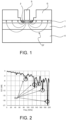
- FIG. 1 is a cross-sectional view showing an example of a conventional optical waveguide element.
- an optical waveguide 2 is formed by thermally diffusing Ti or the like on a substrate 1 having an electro-optic effect, such as lithium niobate (LN).
- a control electrode for applying an electric field to the optical waveguide is formed on the substrate 1, and specifically, a signal electrode S and a ground electrode G sandwiching the signal electrode S are formed.
- the lower portion of the ground electrode has a shape protruding toward the signal electrode side. This is because the electric field applied to the optical waveguide is enhanced by narrowing the distance between the signal electrode and the ground electrode in the vicinity of the optical waveguide. Another reason is that, by widening the distance between the signal electrode and the ground electrode at the upper portion of the electrode, speed matching is realized between a light wave propagating through the optical waveguide and a microwave propagating through the signal electrode, and impedance of the control electrode is increased, for example, to close to 50 ⁇ of an input impedance.
- FIG. 1 by reducing the thickness of the substrate 1, the efficiency of the electric field applied to the optical waveguide is improved.
- a holding substrate 4 is bonded via an adhesive layer 3 to reinforce the mechanical strength of the thin substrate 1.
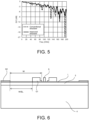
- FIG. 2 shows frequency characteristics of the optical waveguide element as shown in FIG. 1 .
- the horizontal axis of FIG. 2 represents a frequency of the microwave applied to the optical waveguide element, and the vertical axis represents loss (insertion loss) of transmission characteristics (S21) of the optical waveguide element.
- a so-called dip phenomenon occurs, in which the waveform is greatly depressed (dropped) in high frequency bands.
- the electric field (electric field lines EF) formed by the control electrode spreads not only in the substrate 1 but over the entirety including the holding substrate 4, and the high-frequency microwave applied to the signal electrode is coupled with a resonance mode (substrate mode) in the substrate.
- Patent Document 1 has disclosed that a low dielectric constant portion is locally formed in a holding substrate (reinforcing substrate).
- the method disclosed in Patent Document 1 has problems of complicating the manufacturing process of the holding substrate 4 and increasing the manufacturing cost.
- An objective of the disclosure is to provide an optical waveguide element which solves the above-described problems, suppresses the dip phenomenon of frequency characteristics, and suppresses an increase in manufacturing cost. Further, the disclosure provides an optical modulation device and an optical transmission device using the optical waveguide element.
- an optical waveguide element, and an optical modulation device and an optical transmission device using the same according to the disclosure include the following technical features.
- the disclosure provides an optical waveguide element including a substrate having an electro-optic effect, an optical waveguide formed in the substrate, and a control electrode arranged on the substrate to modulate a light wave propagating through the optical waveguide.
- the control electrode includes a signal electrode and a ground electrode.
- the signal electrode and the ground electrode are arranged along a modulation effect portion of the optical waveguide that performs modulation.
- a slit separating the ground electrode into a first ground electrode close to the signal electrode and a second ground electrode far from the signal electrode is formed in a range corresponding to the modulation effect portion. Therefore, coupling with the substrate mode is suppressed, and the dip phenomenon of the frequency characteristics is suppressed.
- an increase in manufacturing cost can also be suppressed.
- the optical waveguide element of the disclosure includes a substrate 1 having an electro-optic effect, an optical waveguide 2 formed in the substrate, and a control electrode arranged on the substrate 1 to modulate a light wave propagating through the optical waveguide.
- the optical waveguide element is characterized in that the control electrode includes a signal electrode S and a ground electrode, and the signal electrode S and the ground electrode are arranged along a modulation effect portion of the optical waveguide that performs modulation.
- a slit SL separating the ground electrode into a first ground electrode G1 close to the signal electrode S and a second ground electrode G2 far from the signal electrode S is formed in a range corresponding to the modulation effect portion.
- the material of the substrate 1 used in the optical waveguide element of the disclosure may include a ferroelectric material having an electro-optic effect, specifically, a substrate of lithium niobate (LN), lithium tantalate (LT), PLZT (lead lanthanum zirconate titanate), or a vapor-phase growth film made of these materials.
- a ferroelectric material having an electro-optic effect specifically, a substrate of lithium niobate (LN), lithium tantalate (LT), PLZT (lead lanthanum zirconate titanate), or a vapor-phase growth film made of these materials.
- Various materials such as semiconductor materials and organic materials may also be used as the substrate of the optical waveguide element.
- the thickness of the substrate 1 in which the optical waveguide is formed may be set to 20 ⁇ m or less, preferably 10 ⁇ m or less, and more preferably 5 ⁇ m or less or 2 ⁇ m or less.
- a holding substrate 4 having a thickness of 0.2 to 1 mm is attached via an adhesive layer (adhesive) having a thickness of about 20 to 80 ⁇ m, or the holding substrate and the substrate are directly bonded together. LN or the like may be used as the holding substrate.
- the method of forming the optical waveguide in the substrate 1 may include the following methods: a high refractive index type optical waveguide is formed by a method of thermally diffusing a high refractive index material such as Ti on a substrate or by a proton exchange method, or a rib-type optical waveguide in which a portion of the substrate corresponding to the optical waveguide is configured in a protruding shape is formed by etching the substrate or forming grooves on two sides of the optical waveguide.
- the feature of the optical waveguide element of the disclosure lies in that the ground electrode facing the signal electrode S is separated into the first ground electrode G1 and the second ground electrode G2 by using a slit.
- the slit SL may penetrate the ground electrode.
- the electric field (electric field lines EF) formed by the signal electrode S and the ground electrode concentrates on the first ground electrode, and coupling is suppressed between the frequency of a modulation signal and a substrate mode, which is a resonance mode of the entire substrate (including the substrate 1, the adhesive layer 3, and the holding substrate 4) including the holding substrate 4.
- FIG. 5 is a graph displaying a simulation result of frequency characteristics of the disclosure in the case where a width of the first ground electrode G1 is set to 48 ⁇ m and a slit width is set to 410 ⁇ m in FIG. 3 , superimposed with frequency characteristics (simulation result) of the conventional structure of FIG. 1 .
- a width of the first ground electrode G1 is set to 48 ⁇ m and a slit width is set to 410 ⁇ m in FIG. 3 , superimposed with frequency characteristics (simulation result) of the conventional structure of FIG. 1 .
- the optical waveguide element of the disclosure can suppress the dip phenomenon more effectively.
- the first ground electrode G1 has been provided to sandwich the signal electrode S
- the second ground electrode G2 has been provided on a side of the first ground electrode G1 opposite to the signal electrode S.
- a width of the slit SL located between the first ground electrode G1 and the second ground electrode G2 has been set as WSL.
- a total width (length) of the width of the first ground electrode G1 and the width of the slit SL has been set as W.
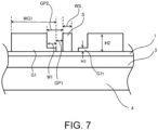
- FIG. 7 is a view illustrating various parameters which define the shapes of the signal electrode S and the first ground electrode G1.
- Each parameter has been set as follows, and the slit width WSL has been varied in the range of 0 to 80 ⁇ m.
- the thickness of the substrate 1 has been set to 9 ⁇ m
- the thickness of the adhesive layer 3 has been set to 55 ⁇ m
- the thickness of the holding substrate 4 has been set to 500 ⁇ m.
- FIG. 8B the approximate curve obtained in FIG. 8A was fit with respect to the frequency characteristics in the case of varying the slit width WSL, and a maximum deviation amount ( ⁇ max) of the frequency characteristics was measured from the approximate curve. It is evaluated that the larger the deviation amount ( ⁇ max) is, the lower the effect of improving the frequency characteristic is.
- FIG. 9 is a graph showing the deviation amount with respect to the slit width WSL, and the deviation amount tends to decrease as the slit width WSL increases. Specifically, it is understood that when the slit width WSL is 20 ⁇ m or more, the decreasing tendency becomes significant, and in particular, in the case where the slit width WSL is 40 ⁇ m or more, there is almost no change in the deviation amount, and the effect is stable. It is assumed that this is because the effect of separating the first ground electrode and the second ground electrode is weakened when the slit width is narrowed.
- the slit width WSL it is preferable to set the slit width WSL to 20 ⁇ m or more, and more preferably, to 40 ⁇ m or more.
- the width WG1 of the first ground electrode has been varied in the range of 48 (30+18) ⁇ m to 418 (400+18) ⁇ m.
- the thickness of the substrate 1 has been set to 9 ⁇ m, the thickness of the adhesive layer 3 has been set to 55 ⁇ m, and the thickness of the holding substrate 4 has been set to 500 ⁇ m.
- FIG. 10 is a graph showing the deviation amount with respect to the width WG1 of the first ground electrode, and as for the width of the first ground electrode (GND), the horizontal axis indicates a value of the width (WG1 - W1) of a bottom surface portion excluding the protruding portion G1t.
- the width (width of the bottom surface portion of the first ground electrode) WG1 of the first ground electrode is 170 ⁇ m or less, and more preferably, to 100 ⁇ m or less.
- the slit width (WSL) and the width (WG1) of the bottom surface portion of the first ground electrode have been examined separately, in general, the larger the slit width is with respect to the width of the first ground electrode, the more the electric field concentrates on the first ground electrode; the smaller the slit width is with respect to the width of the first ground electrode, the more the electric field is also distributed to the second ground electrode.
- Patent Document 2 for speed matching, low switching voltage (low drive voltage), and impedance matching, it has been disclosed to set the width of the earth electrode (ground electrode) to be three times or less the width of the thermal electrode (signal electrode).
- suppression of the dip phenomenon which is a problem addressed by the optical waveguide element of the disclosure, or the second ground electrode and the slit between the first ground electrode and the second ground electrode necessary for the configuration of the disclosure were not mentioned at all.
- substrates such as LN are prone to cracks during cutting.
- this phenomenon becomes significant.
- the dip phenomenon is suppressed and occurrence of cracks is also prevented.
- the shape of the first ground electrode has an L-shaped multi-step structure in which the lower portion is closer to the signal electrode than the upper portion, and the width W1 of the portion G1t in which the lower portion protrudes toward the signal electrode side more than the upper portion in a direction perpendicular to the extending direction of the modulation effect portion is set to a range of 20 to 70% of the width WS of the signal electrode.
- the shape of the first ground electrode has an L-shaped multi-step structure in which the lower portion is closer to the signal electrode than the upper portion, the height HI of the lower portion is 2 to 10 ⁇ m, and the total height of the lower portion and the upper portion is 20 to 50 ⁇ m.
- the portion where the signal electrode and two branch waveguides are parallel to each other is the "modulation effect portion (FP)".
- the slit of the ground electrode is formed over the entire region of the modulation effect portion.
- the ground electrode is separated into the first ground electrode and the second ground electrode by the slit, but preferably the two are electrically connected and kept at the same potential. Therefore, as shown in FIG. 11 , it is also possible to provide an electrical connection portion (dotted line frame A in FIG. 11 ) between the first ground electrode and the second ground electrode outside a range FP corresponding to the modulation effect portion of the optical waveguide. Moreover, as shown in FIG. 12 , it is also possible to electrically connect the first ground electrode G1 and the second ground electrode G2 by wire bonding (WB). In addition to wire bonding, various configurations may also be used to electrically connect the first ground electrode G1 and the second ground electrode G2 at least partially to each other.
- WB wire bonding
- ground electrodes may be arranged between optical waveguides (between 22 and 23).
- the ground electrode G31 serves as the first ground electrode
- the ground electrode G32 serves as the second ground electrode.
- a slit SL3 is provided.
- the ground electrode G32 serves as the first ground electrode
- the ground electrode G31 serves as the second ground electrode.
- the width of the slit SL is preferably 40 ⁇ m or more, and the width of each ground electrode (G31, G32) is preferably 100 ⁇ m or less.
- G11 and G12 indicate first ground electrodes, and G21 and G22 indicate second ground electrodes.
- SL1 and SL2 indicate slits.
- the optical waveguides are 21 to 24.
- 21 and 22 indicate branch waveguides of one Mach-Zehnder optical waveguide
- 23 and 24 indicate branch waveguides of another Mach-Zehnder optical waveguide.
- an optical waveguide element OE of the disclosure provides a modulation electrode (control electrode, not shown) which modulates a light wave propagating through an optical waveguide OW in a substrate and is accommodated in a housing CS.
- an optical modulation device MD can be configured by providing an optical fiber FB which inputs and outputs light waves (input light Lin and output light Lout) from and to the optical waveguide OW.
- the optical fiber may not only be arranged outside the housing CS as shown in FIG. 14 , but may also be introduced and fixed into the housing via a through-hole penetrating a sidewall of the housing.
- a sign PC indicates a polarization combining means.
- An optical transmission device OTA may be configured by connecting, to the optical modulation device MD, an electronic circuit (digital signal processor DSP) which outputs a modulation signal So causing the optical modulation device MD to perform a modulating operation.
- a driver circuit DRV is used since a modulation signal Sin applied to the optical waveguide element needs to be amplified.
- the driver circuit DRV and the digital signal processor DSP may be arranged outside the housing CS, but may also be arranged inside the housing CS. In particular, by arranging the driver circuit DRV inside the housing, it is possible to further reduce the propagation loss of the modulation signal from the driver circuit.
- an optical waveguide element which suppresses the dip phenomenon of frequency characteristics and suppresses an increase in manufacturing cost. Also, it is possible to provide an optical modulation device and an optical transmission device using the optical waveguide element.
Landscapes
- Physics & Mathematics (AREA)
- Nonlinear Science (AREA)
- General Physics & Mathematics (AREA)
- Optics & Photonics (AREA)
- Chemical & Material Sciences (AREA)
- Engineering & Computer Science (AREA)
- Ceramic Engineering (AREA)
- Crystallography & Structural Chemistry (AREA)
- Optical Modulation, Optical Deflection, Nonlinear Optics, Optical Demodulation, Optical Logic Elements (AREA)
Abstract
Description
- The disclosure relates to an optical waveguide element, and an optical modulation device and an optical transmission device using the same, and more particularly, to an optical waveguide element which suppresses a dip phenomenon of high frequency characteristics.
- Optical waveguide elements, e.g., optical modulators, using substrates formed with optical waveguides are widely used in the fields of optical measurement technology and optical communication technology. In recent years, there has been a demand for the use of optical modulators in higher frequency bands (e.g., 30 to 300 GHz) to respond to the increasing traffic volume of mobile communications.
-
FIG. 1 is a cross-sectional view showing an example of a conventional optical waveguide element. InFIG. 1 , anoptical waveguide 2 is formed by thermally diffusing Ti or the like on asubstrate 1 having an electro-optic effect, such as lithium niobate (LN). A control electrode for applying an electric field to the optical waveguide is formed on thesubstrate 1, and specifically, a signal electrode S and a ground electrode G sandwiching the signal electrode S are formed. - The lower portion of the ground electrode has a shape protruding toward the signal electrode side. This is because the electric field applied to the optical waveguide is enhanced by narrowing the distance between the signal electrode and the ground electrode in the vicinity of the optical waveguide. Another reason is that, by widening the distance between the signal electrode and the ground electrode at the upper portion of the electrode, speed matching is realized between a light wave propagating through the optical waveguide and a microwave propagating through the signal electrode, and impedance of the control electrode is increased, for example, to close to 50Ω of an input impedance.
- Further, in
FIG. 1 , by reducing the thickness of thesubstrate 1, the efficiency of the electric field applied to the optical waveguide is improved. Aholding substrate 4 is bonded via anadhesive layer 3 to reinforce the mechanical strength of thethin substrate 1. -
FIG. 2 shows frequency characteristics of the optical waveguide element as shown inFIG. 1 . The horizontal axis ofFIG. 2 represents a frequency of the microwave applied to the optical waveguide element, and the vertical axis represents loss (insertion loss) of transmission characteristics (S21) of the optical waveguide element. Referring to the frequency characteristics ofFIG. 2 , a so-called dip phenomenon occurs, in which the waveform is greatly depressed (dropped) in high frequency bands. - The reason lies in that, as shown in
FIG. 1 , the electric field (electric field lines EF) formed by the control electrode spreads not only in thesubstrate 1 but over the entirety including theholding substrate 4, and the high-frequency microwave applied to the signal electrode is coupled with a resonance mode (substrate mode) in the substrate. - To suppress such a dip (ripple) phenomenon,
Patent Document 1 has disclosed that a low dielectric constant portion is locally formed in a holding substrate (reinforcing substrate). The method disclosed inPatent Document 1 has problems of complicating the manufacturing process of theholding substrate 4 and increasing the manufacturing cost. -
- [Patent Document 1]
Japanese Patent Application Laid-Open No. 2019-174588 - [Patent Document 2]
Japanese Patent Application Laid-Open No. H5-196902 - An objective of the disclosure is to provide an optical waveguide element which solves the above-described problems, suppresses the dip phenomenon of frequency characteristics, and suppresses an increase in manufacturing cost. Further, the disclosure provides an optical modulation device and an optical transmission device using the optical waveguide element.
- To solve the above problems, an optical waveguide element, and an optical modulation device and an optical transmission device using the same according to the disclosure include the following technical features.
- (1) An optical waveguide element includes a substrate having an electro-optic effect, an optical waveguide formed in the substrate, and a control electrode arranged on the substrate to modulate a light wave propagating through the optical waveguide. The control electrode includes a signal electrode and a ground electrode. The signal electrode and the ground electrode are arranged along a modulation effect portion of the optical waveguide that performs modulation. In a shape of a bottom surface of the ground electrode facing the substrate, a slit separating the ground electrode into a first ground electrode close to the signal electrode and a second ground electrode far from the signal electrode is formed in a range corresponding to the modulation effect portion.
- (2) In the optical waveguide element according to (1) above, a width of the slit in a direction perpendicular to an extending direction of the modulation effect portion is 40 µm or more.
- (3) In the optical waveguide element according to (1) or (2) above, a width of a bottom surface portion of the first ground electrode in a direction perpendicular to an extending direction of the modulation effect portion is 100 µm or less.
- (4) In the optical waveguide element according to any one of (1) to (3) above, a ratio (WSL/WG1) of a width (WSL) of the slit in a direction perpendicular to an extending direction of the modulation effect portion to a width (WG1) of a bottom surface portion of the first ground electrode in the direction perpendicular to the extending direction of the modulation effect portion is 0.4 or more.
- (5) In the optical waveguide element according to any one of (1) to (4) above, a shape of the first ground electrode has an L-shaped multi-step structure in which a lower portion is closer to the signal electrode than an upper portion. A width of the lower portion protruding toward a signal electrode side more than the upper portion in a direction perpendicular to an extending direction of the modulation effect portion is set to a range of 20 to 70% of a width of the signal electrode.
- (6) In the optical waveguide element according to any one of (1) to (5) above, a shape of the first ground electrode has an L-shaped multi-step structure in which a lower portion is closer to the signal electrode than an upper portion. A height of the lower portion is 2 to 10 µm. A total height of the lower portion and the upper portion is 20 to 50 µm.
- (7) In the optical waveguide element according to any one of (1) to (6) above, the first ground electrode and the second ground electrode are electrically connected to each other outside the range corresponding to the modulation effect portion of the optical waveguide.
- (8) In the optical waveguide element according to any one of (1) to (7) above, the substrate has a thickness of 20 µm or less. A holding substrate is arranged on a back side of the substrate via an adhesive layer.
- (9) In an optical modulation device, the optical waveguide element according to any one of (1) to (8) above is accommodated in a housing, and the optical modulation device includes an optical fiber which inputs or outputs a light wave from or to the optical waveguide.
- (10) The optical modulation device according to (9) above includes an electronic circuit inside the housing to amplify a modulation signal inputted to the signal electrode of the optical waveguide element.
- (11) An optical transmission device includes the optical modulation device according to (9) or (10) above, and an electronic circuit which outputs a modulation signal causing the optical modulation device to perform a modulation operation.
- The disclosure provides an optical waveguide element including a substrate having an electro-optic effect, an optical waveguide formed in the substrate, and a control electrode arranged on the substrate to modulate a light wave propagating through the optical waveguide. The control electrode includes a signal electrode and a ground electrode. The signal electrode and the ground electrode are arranged along a modulation effect portion of the optical waveguide that performs modulation. In a shape of a bottom surface of the ground electrode facing the substrate, a slit separating the ground electrode into a first ground electrode close to the signal electrode and a second ground electrode far from the signal electrode is formed in a range corresponding to the modulation effect portion. Therefore, coupling with the substrate mode is suppressed, and the dip phenomenon of the frequency characteristics is suppressed. Moreover, since only the shape of the control electrode is changed, an increase in manufacturing cost can also be suppressed.
-
-
FIG. 1 is a cross-sectional view illustrating a structure of a conventional optical waveguide element. -
FIG. 2 is a graph showing frequency characteristics related to the optical waveguide element ofFIG. 1 . -
FIG. 3 is a cross-sectional view illustrating an embodiment related to an optical waveguide element of the disclosure. -
FIG. 4 is a view illustrating electric field lines (electric field distribution) related to the optical waveguide element ofFIG. 3 . -
FIG. 5 is a graph showing frequency characteristics related to the optical waveguide element of the disclosure. -
FIG. 6 is a view illustrating a simulation model related to the optical waveguide element of the disclosure. -
FIG. 7 is an enlarged view of the vicinity of a signal electrode S inFIG. 6 . -
FIG. 8A and FIG. 8B are graphs illustrating a method of evaluating frequency characteristics.FIG. 8A shows suitable frequency characteristics and an approximate curve (fitting curve) thereof.FIG. 8B shows the approximate curve ofFIG. 8A and frequency characteristic to be evaluated. -
FIG. 9 is a graph illustrating a relationship between a width of a slit used in the optical waveguide element of the disclosure and a deviation amount from the approximate curve (fitting curve). -
FIG. 10 is a graph illustrating a relationship between a width of a first ground electrode used in the optical waveguide element of the disclosure and a deviation amount from the approximate curve (fitting curve). -
FIG. 11 is a view illustrating an arrangement relationship between a modulation effect portion and the slit in the optical waveguide element of the disclosure. -
FIG. 12 is a view illustrating another electrical connection between a first ground electrode G1 and a second ground electrode G2 related to the optical waveguide element of the disclosure. -
FIG. 13 is a view illustrating an application example in which a plurality of Mach-Zehnder optical waveguides are provided in the optical waveguide element of the disclosure. -
FIG. 14 is a plan view illustrating an optical modulation device and an optical transmission device according to the disclosure. - Hereinafter, an optical waveguide element of the disclosure will be described in detail with reference to preferred examples.
- As shown in
FIG. 3 , the optical waveguide element of the disclosure includes asubstrate 1 having an electro-optic effect, anoptical waveguide 2 formed in the substrate, and a control electrode arranged on thesubstrate 1 to modulate a light wave propagating through the optical waveguide. The optical waveguide element is characterized in that the control electrode includes a signal electrode S and a ground electrode, and the signal electrode S and the ground electrode are arranged along a modulation effect portion of the optical waveguide that performs modulation. In the shape of a bottom surface of the ground electrode facing the substrate, a slit SL separating the ground electrode into a first ground electrode G1 close to the signal electrode S and a second ground electrode G2 far from the signal electrode S is formed in a range corresponding to the modulation effect portion. - The material of the
substrate 1 used in the optical waveguide element of the disclosure may include a ferroelectric material having an electro-optic effect, specifically, a substrate of lithium niobate (LN), lithium tantalate (LT), PLZT (lead lanthanum zirconate titanate), or a vapor-phase growth film made of these materials. Various materials such as semiconductor materials and organic materials may also be used as the substrate of the optical waveguide element. - To improve the electric field efficiency applied to the optical waveguide, the thickness of the
substrate 1 in which the optical waveguide is formed may be set to 20 µm or less, preferably 10 µm or less, and more preferably 5 µm or less or 2 µm or less. In such cases, to reinforce the mechanical strength of thesubstrate 1, for example, a holdingsubstrate 4 having a thickness of 0.2 to 1 mm is attached via an adhesive layer (adhesive) having a thickness of about 20 to 80 µm, or the holding substrate and the substrate are directly bonded together. LN or the like may be used as the holding substrate. - The method of forming the optical waveguide in the
substrate 1 may include the following methods: a high refractive index type optical waveguide is formed by a method of thermally diffusing a high refractive index material such as Ti on a substrate or by a proton exchange method, or a rib-type optical waveguide in which a portion of the substrate corresponding to the optical waveguide is configured in a protruding shape is formed by etching the substrate or forming grooves on two sides of the optical waveguide. - As shown in
FIG. 3 , the feature of the optical waveguide element of the disclosure lies in that the ground electrode facing the signal electrode S is separated into the first ground electrode G1 and the second ground electrode G2 by using a slit. As for the shape of the slit, as shown inFIG. 3 , the slit SL may penetrate the ground electrode. - By separating the ground electrode into the first ground electrode and the second ground electrode as in the disclosure, as shown in
FIG. 4 , the electric field (electric field lines EF) formed by the signal electrode S and the ground electrode concentrates on the first ground electrode, and coupling is suppressed between the frequency of a modulation signal and a substrate mode, which is a resonance mode of the entire substrate (including thesubstrate 1, theadhesive layer 3, and the holding substrate 4) including the holdingsubstrate 4. -
FIG. 5 is a graph displaying a simulation result of frequency characteristics of the disclosure in the case where a width of the first ground electrode G1 is set to 48 µm and a slit width is set to 410 µm inFIG. 3 , superimposed with frequency characteristics (simulation result) of the conventional structure ofFIG. 1 . Referring to the graph ofFIG. 5 , it is easily understood that the optical waveguide element of the disclosure can suppress the dip phenomenon more effectively. - To explore the shape of the control electrode suitable for the optical waveguide element of the disclosure, the models shown in
FIG. 6 andFIG. 7 have been set and simulations have been performed. - In
FIG. 6 , the first ground electrode G1 has been provided to sandwich the signal electrode S, and the second ground electrode G2 has been provided on a side of the first ground electrode G1 opposite to the signal electrode S. A width of the slit SL located between the first ground electrode G1 and the second ground electrode G2 has been set as WSL. A total width (length) of the width of the first ground electrode G1 and the width of the slit SL has been set as W. -
FIG. 7 is a view illustrating various parameters which define the shapes of the signal electrode S and the first ground electrode G1. - The definition of each parameter is as follows.
- WS: width of the signal electrode
- WG1: width of the first ground electrode
- W1: width of a portion (G1t) protruding toward the signal electrode side at a lower portion of the first ground electrode
- H1: height of the portion (G1t) protruding toward the signal electrode side at the lower portion of the first ground electrode
- H2: height of the first ground electrode
- GP1: distance (gap) between the signal electrode and the protruding portion (G1t) of the first ground electrode
- GP2: distance (gap) between the signal electrode and an upper portion of the first ground electrode
- WSL: width of the slit
- W: WG1 + WSL
- The following simulation has been performed to investigate an optimum value for the width of the slit SL.
- Each parameter has been set as follows, and the slit width WSL has been varied in the range of 0 to 80 µm.
- WS: 30 µm
- WG1: 48 µm
- W1: 18 µm
- H1: 4.5 µm
- H2: 40 µm
- GP1: 20 µm
- GP2: 38 µm
- Further, the thickness of the
substrate 1 has been set to 9 µm, the thickness of theadhesive layer 3 has been set to 55 µm, and the thickness of the holdingsubstrate 4 has been set to 500 µm. - To evaluate the frequency characteristics, the size of the dip has been measured using an approximate curve (fitting curve) as shown in
FIG. 8A and FIG. 8B . Specifically,FIG. 8A shows the frequency characteristics of WSL = 80 µm, and an approximate curve has been set based on this graph. Next, as shown inFIG. 8B , the approximate curve obtained inFIG. 8A was fit with respect to the frequency characteristics in the case of varying the slit width WSL, and a maximum deviation amount (δmax) of the frequency characteristics was measured from the approximate curve. It is evaluated that the larger the deviation amount (δmax) is, the lower the effect of improving the frequency characteristic is. -
FIG. 9 is a graph showing the deviation amount with respect to the slit width WSL, and the deviation amount tends to decrease as the slit width WSL increases. Specifically, it is understood that when the slit width WSL is 20 µm or more, the decreasing tendency becomes significant, and in particular, in the case where the slit width WSL is 40 µm or more, there is almost no change in the deviation amount, and the effect is stable. It is assumed that this is because the effect of separating the first ground electrode and the second ground electrode is weakened when the slit width is narrowed. - Based on the above, it is preferable to set the slit width WSL to 20 µm or more, and more preferably, to 40 µm or more.
- Next, to investigate an optimum value for the width WG1 of the first ground electrode, a simulation has been performed under the following conditions. The width WG1 of the first ground electrode has been varied in the range of 48 (30+18) µm to 418 (400+18) µm.
- WS: 30 µm
- W1: 18 µm
- H1: 4.5 µm
- H2: 40 µm
- GP1: 20 µm
- GP2: 38 µm
- WSL: 80 µm
- The thickness of the
substrate 1 has been set to 9 µm, the thickness of theadhesive layer 3 has been set to 55 µm, and the thickness of the holdingsubstrate 4 has been set to 500 µm. - Further, evaluation of the obtained frequency characteristics has been performed in the same manner as the evaluation using the approximate curve (fitting curve) described above.
-
FIG. 10 is a graph showing the deviation amount with respect to the width WG1 of the first ground electrode, and as for the width of the first ground electrode (GND), the horizontal axis indicates a value of the width (WG1 - W1) of a bottom surface portion excluding the protruding portion G1t. - Referring to
FIG. 10 , a tendency of decrease in the deviation amount starts around a point where the width (WG1 - W1) of the bottom surface portion is 150 µm (WG1 = 168 µm), and in particular, in the case of 80 µm (WG1 = 98 µm) or less, the deviation amount is more effectively suppressed to a low level, and the effect of improving the frequency characteristics is expected. It is assumed that this is because it is preferable to set the width of the first ground electrode to be narrower to suppress the spread of the electric field lines and locally form the electric field. - Based on the above, it is preferable to set the width (width of the bottom surface portion of the first ground electrode) WG1 of the first ground electrode to 170 µm or less, and more preferably, to 100 µm or less.
- In the above, although the slit width (WSL) and the width (WG1) of the bottom surface portion of the first ground electrode have been examined separately, in general, the larger the slit width is with respect to the width of the first ground electrode, the more the electric field concentrates on the first ground electrode; the smaller the slit width is with respect to the width of the first ground electrode, the more the electric field is also distributed to the second ground electrode. Therefore, there is a correlation between the slit width (WSL) and the width (WG1) of the bottom surface portion of the first ground electrode, and with reference to the above simulation results, upon calculating the ratio between the two (WSL/WG1), it is understood that the effect of the slit starts to appear at the ratio of 0.4 or more, and the effect becomes more significant when the ratio becomes 0.8 or more.
- In addition, in
Patent Document 2, for speed matching, low switching voltage (low drive voltage), and impedance matching, it has been disclosed to set the width of the earth electrode (ground electrode) to be three times or less the width of the thermal electrode (signal electrode). However, inPatent Document 2, suppression of the dip phenomenon, which is a problem addressed by the optical waveguide element of the disclosure, or the second ground electrode and the slit between the first ground electrode and the second ground electrode necessary for the configuration of the disclosure were not mentioned at all. - Also, substrates such as LN are prone to cracks during cutting. In particular, in the case where a thin LN substrate is used, this phenomenon becomes significant. To prevent occurrence of cracks, it is preferable to dispose the electrodes over the entire surface of the substrate and to the edges of the substrate, as shown in
FIG. 1 . In the disclosure, by providing a slit in the ground electrode, the dip phenomenon is suppressed and occurrence of cracks is also prevented. - As shown in
FIG. 7 , preferably, the shape of the first ground electrode has an L-shaped multi-step structure in which the lower portion is closer to the signal electrode than the upper portion, and the width W1 of the portion G1t in which the lower portion protrudes toward the signal electrode side more than the upper portion in a direction perpendicular to the extending direction of the modulation effect portion is set to a range of 20 to 70% of the width WS of the signal electrode. - Further, as shown in
FIG. 7 , preferably, the shape of the first ground electrode has an L-shaped multi-step structure in which the lower portion is closer to the signal electrode than the upper portion, the height HI of the lower portion is 2 to 10 µm, and the total height of the lower portion and the upper portion is 20 to 50 µm. - As shown in
FIG. 11 , in the case where the optical waveguide is a Mach-Zehnder optical waveguide, the portion where the signal electrode and two branch waveguides are parallel to each other is the "modulation effect portion (FP)". Preferably, the slit of the ground electrode is formed over the entire region of the modulation effect portion. By forming the slit of the ground electrode over the entire region of the modulation effect portion, it is possible to provide an optical waveguide element in which coupling with the substrate mode is suppressed and the dip phenomenon of the frequency characteristics is suppressed. - As described above, the ground electrode is separated into the first ground electrode and the second ground electrode by the slit, but preferably the two are electrically connected and kept at the same potential. Therefore, as shown in
FIG. 11 , it is also possible to provide an electrical connection portion (dotted line frame A inFIG. 11 ) between the first ground electrode and the second ground electrode outside a range FP corresponding to the modulation effect portion of the optical waveguide. Moreover, as shown inFIG. 12 , it is also possible to electrically connect the first ground electrode G1 and the second ground electrode G2 by wire bonding (WB). In addition to wire bonding, various configurations may also be used to electrically connect the first ground electrode G1 and the second ground electrode G2 at least partially to each other. - In cases of arranging a plurality of optical waveguides side by side in a substrate, or arranging a plurality of Mach-Zehnder optical waveguides side by side, as shown in
FIG. 13 , ground electrodes (G31, G32) may be arranged between optical waveguides (between 22 and 23). In such cases, when viewed from a signal electrode S1, the ground electrode G31 serves as the first ground electrode, and the ground electrode G32 serves as the second ground electrode. A slit SL3 is provided. On the other hand, when viewed from a signal electrode S2, the ground electrode G32 serves as the first ground electrode, and the ground electrode G31 serves as the second ground electrode. Therefore, the width of the slit SL is preferably 40 µm or more, and the width of each ground electrode (G31, G32) is preferably 100 µm or less. Regarding other signs inFIG. 13 , G11 and G12 indicate first ground electrodes, and G21 and G22 indicate second ground electrodes. SL1 and SL2 indicate slits. The optical waveguides are 21 to 24. For example, 21 and 22 indicate branch waveguides of one Mach-Zehnder optical waveguide, and 23 and 24 indicate branch waveguides of another Mach-Zehnder optical waveguide. - As shown in
FIG. 14 , an optical waveguide element OE of the disclosure provides a modulation electrode (control electrode, not shown) which modulates a light wave propagating through an optical waveguide OW in a substrate and is accommodated in a housing CS. Furthermore, an optical modulation device MD can be configured by providing an optical fiber FB which inputs and outputs light waves (input light Lin and output light Lout) from and to the optical waveguide OW. The optical fiber may not only be arranged outside the housing CS as shown inFIG. 14 , but may also be introduced and fixed into the housing via a through-hole penetrating a sidewall of the housing. A sign PC indicates a polarization combining means. - An optical transmission device OTA may be configured by connecting, to the optical modulation device MD, an electronic circuit (digital signal processor DSP) which outputs a modulation signal So causing the optical modulation device MD to perform a modulating operation. A driver circuit DRV is used since a modulation signal Sin applied to the optical waveguide element needs to be amplified. The driver circuit DRV and the digital signal processor DSP may be arranged outside the housing CS, but may also be arranged inside the housing CS. In particular, by arranging the driver circuit DRV inside the housing, it is possible to further reduce the propagation loss of the modulation signal from the driver circuit.
- As described above, according to the disclosure, it is possible to provide an optical waveguide element which suppresses the dip phenomenon of frequency characteristics and suppresses an increase in manufacturing cost. Also, it is possible to provide an optical modulation device and an optical transmission device using the optical waveguide element.
-
- [0049] 1
- Substrate
- 2
- Optical waveguide
- 3
- Adhesive layer
- 4
- Holding substrate
- SL
- Slit
- G1
- First ground electrode
- G2
- Second ground electrode
- OE
- Optical waveguide element
- MD
- Optical modulation device
- OTA
- Optical transmission device
Claims (11)
- An optical waveguide element (OE) comprising:a substrate (1) having an electro-optic effect;an optical waveguide (2, 21 to 24, OW) formed in the substrate (1); anda control electrode arranged on the substrate (1) to modulate a light wave propagating through the optical waveguide (2, 21 to 24, OW),wherein the control electrode comprises a signal electrode (S, S1, S2) and a ground electrode,the signal electrode (S, S1, S2) and the ground electrode are arranged along a modulation effect portion of the optical waveguide (2, 21 to 24, OW) that performs modulation, andin a shape of a bottom surface of the ground electrode facing the substrate (1), a slit (SL, SL1, SL2, SL3) separating the ground electrode into a first ground electrode (G1) close to the signal electrode (S, S1, S2) and a second ground electrode (G2) far from the signal electrode (S, S1, S2) is formed in a range corresponding to the modulation effect portion.
- The optical waveguide element (OE) according to claim 1, wherein a width of the slit (SL, SL1, SL2, SL3) in a direction perpendicular to an extending direction of the modulation effect portion is 40 µm or more.
- The optical waveguide element (OE) according to claim 1 or 2, wherein a width of a bottom surface portion of the first ground electrode (G1) in a direction perpendicular to an extending direction of the modulation effect portion is 100 µm or less.
- The optical waveguide element (OE) according to any one of claims 1 to 3, wherein a ratio (WSL/WG1) of a width (WSL) of the slit (SL, SL1, SL2, SL3) in a direction perpendicular to an extending direction of the modulation effect portion to a width (WG1) of a bottom surface portion of the first ground electrode (G1) in the direction perpendicular to the extending direction of the modulation effect portion is 0.4 or more.
- The optical waveguide element (OE) according to any one of claims 1 to 4, wherein a shape of the first ground electrode (G1) has an L-shaped multi-step structure in which a lower portion is closer to the signal electrode (S, S1, S2) than an upper portion, and
a width of the lower portion protruding toward a signal electrode side more than the upper portion in a direction perpendicular to an extending direction of the modulation effect portion is set to a range of 20 to 70% of a width of the signal electrode (S, S1, S2). - The optical waveguide element (OE) according to any one of claims 1 to 5, wherein a shape of the first ground electrode (G1) has an L-shaped multi-step structure in which a lower portion is closer to the signal electrode (S, S1, S2) than an upper portion,a height of the lower portion is 2 to 10 µm, anda total height of the lower portion and the upper portion is 20 to 50 µm.
- The optical waveguide element (OE) according to any one of claims 1 to 6, wherein the first ground electrode (G1) and the second ground electrode (G2) are electrically connected to each other outside the range corresponding to the modulation effect portion of the optical waveguide (2, 21 to 24, OW).
- The optical waveguide element (OE) according to any one of claims 1 to 7, wherein the substrate (1) has a thickness of 20 µm or less, and
a holding substrate (4) is arranged on a back side of the substrate (1) via an adhesive layer (3). - An optical modulation device (MD), wherein the optical waveguide element (OE) according to any one of claims 1 to 8 is accommodated in a housing (CS), and the optical modulation device (MD) comprises an optical fiber (FB) which inputs or outputs a light wave from or to the optical waveguide (2, 21 to 24, OW).
- The optical modulation device (MD) according to claim 9, comprising an electronic circuit (DRV) inside the housing (CS) to amplify a modulation signal inputted to the signal electrode (S, S1, S2) of the optical waveguide element (OE).
- An optical transmission device (OTA) comprising:the optical modulation device (MD) according to claim 9 or 10; andan electronic circuit (DSP) which outputs a modulation signal causing the optical modulation device (MD) to perform a modulation operation.
Applications Claiming Priority (1)
| Application Number | Priority Date | Filing Date | Title |
|---|---|---|---|
| JP2021162200A JP7677102B2 (en) | 2021-09-30 | 2021-09-30 | Optical waveguide element, optical modulation device using the same, and optical transmission device |
Publications (2)
| Publication Number | Publication Date |
|---|---|
| EP4160301A1 true EP4160301A1 (en) | 2023-04-05 |
| EP4160301B1 EP4160301B1 (en) | 2025-06-11 |
Family
ID=83506277
Family Applications (1)
| Application Number | Title | Priority Date | Filing Date |
|---|---|---|---|
| EP22197896.8A Active EP4160301B1 (en) | 2021-09-30 | 2022-09-27 | Optical waveguide element, and optical modulation device and optical transmission device using the same |
Country Status (4)
| Country | Link |
|---|---|
| US (1) | US12153295B2 (en) |
| EP (1) | EP4160301B1 (en) |
| JP (1) | JP7677102B2 (en) |
| CN (2) | CN218524976U (en) |
Citations (7)
| Publication number | Priority date | Publication date | Assignee | Title |
|---|---|---|---|---|
| JPH05196902A (en) | 1991-08-14 | 1993-08-06 | Hewlett Packard Co <Hp> | Traveling-wave optical modulator |
| EP1132764A1 (en) * | 2000-03-08 | 2001-09-12 | JDS Uniphase Corporation | Electro-optic modulator with enhanced temperature stability |
| US20040151414A1 (en) * | 2003-02-05 | 2004-08-05 | Jds Uniphase Corporation | Slotted electrode electro-optic modulator |
| US20180017839A1 (en) * | 2015-03-31 | 2018-01-18 | Sumitomo Osaka Cement Co., Ltd | Optical modulator |
| US20180173026A1 (en) * | 2016-12-16 | 2018-06-21 | Lumentum Operations Llc | Optical modulator |
| JP2019174588A (en) | 2018-03-28 | 2019-10-10 | 住友大阪セメント株式会社 | Optical waveguide element |
| WO2020202596A1 (en) * | 2019-03-29 | 2020-10-08 | 住友大阪セメント株式会社 | Optical modulator |
Family Cites Families (10)
| Publication number | Priority date | Publication date | Assignee | Title |
|---|---|---|---|---|
| JP2713087B2 (en) * | 1993-04-13 | 1998-02-16 | 日本電気株式会社 | Waveguide optical device |
| US5416859A (en) * | 1993-04-14 | 1995-05-16 | The United States Of America As Represented By The Secretary Of The Navy | Broadband, low drive voltage, electrooptic, intergrated optical modulator |
| JP3660529B2 (en) * | 1999-06-21 | 2005-06-15 | 住友大阪セメント株式会社 | Optical waveguide device |
| JP4443011B2 (en) * | 2000-07-27 | 2010-03-31 | 日本碍子株式会社 | Traveling wave type optical modulator |
| US7171063B2 (en) * | 2004-12-01 | 2007-01-30 | Jds Uniphase Corporation | Controllable electro-optic device having substrate trenches between electrodes |
| JP2009086336A (en) * | 2007-09-28 | 2009-04-23 | Sumitomo Osaka Cement Co Ltd | Optical waveguide type device |
| JP6575298B2 (en) * | 2015-10-27 | 2019-09-18 | 住友大阪セメント株式会社 | Light modulator |
| JP7087555B2 (en) * | 2018-03-29 | 2022-06-21 | 住友大阪セメント株式会社 | Optical modulator |
| JP7196736B2 (en) * | 2019-03-29 | 2022-12-27 | 住友大阪セメント株式会社 | Optical waveguide element and optical waveguide device |
| JP7463722B2 (en) * | 2019-12-26 | 2024-04-09 | 住友大阪セメント株式会社 | Optical waveguide element and optical modulator |
-
2021
- 2021-09-30 JP JP2021162200A patent/JP7677102B2/en active Active
-
2022
- 2022-09-27 US US17/954,304 patent/US12153295B2/en active Active
- 2022-09-27 EP EP22197896.8A patent/EP4160301B1/en active Active
- 2022-09-29 CN CN202222611564.1U patent/CN218524976U/en active Active
- 2022-09-29 CN CN202211200726.0A patent/CN115877597A/en active Pending
Patent Citations (7)
| Publication number | Priority date | Publication date | Assignee | Title |
|---|---|---|---|---|
| JPH05196902A (en) | 1991-08-14 | 1993-08-06 | Hewlett Packard Co <Hp> | Traveling-wave optical modulator |
| EP1132764A1 (en) * | 2000-03-08 | 2001-09-12 | JDS Uniphase Corporation | Electro-optic modulator with enhanced temperature stability |
| US20040151414A1 (en) * | 2003-02-05 | 2004-08-05 | Jds Uniphase Corporation | Slotted electrode electro-optic modulator |
| US20180017839A1 (en) * | 2015-03-31 | 2018-01-18 | Sumitomo Osaka Cement Co., Ltd | Optical modulator |
| US20180173026A1 (en) * | 2016-12-16 | 2018-06-21 | Lumentum Operations Llc | Optical modulator |
| JP2019174588A (en) | 2018-03-28 | 2019-10-10 | 住友大阪セメント株式会社 | Optical waveguide element |
| WO2020202596A1 (en) * | 2019-03-29 | 2020-10-08 | 住友大阪セメント株式会社 | Optical modulator |
Also Published As
| Publication number | Publication date |
|---|---|
| US20230096004A1 (en) | 2023-03-30 |
| CN115877597A (en) | 2023-03-31 |
| JP2023051482A (en) | 2023-04-11 |
| CN218524976U (en) | 2023-02-24 |
| JP7677102B2 (en) | 2025-05-15 |
| EP4160301B1 (en) | 2025-06-11 |
| US12153295B2 (en) | 2024-11-26 |
Similar Documents
| Publication | Publication Date | Title |
|---|---|---|
| EP2006723B1 (en) | Light control element | |
| US6741378B2 (en) | Optical modulator having element for varying optical phase by electrooptic effect | |
| US8737773B2 (en) | Optical control element | |
| US5790719A (en) | Optical control device | |
| US8391651B2 (en) | Optical waveguide device | |
| US8792752B2 (en) | Optical waveguide element module | |
| US20130243364A1 (en) | Optical control device | |
| EP2116889A1 (en) | Optical phase modulator | |
| WO2014156459A1 (en) | Optical modulator | |
| US8774564B2 (en) | Optical waveguide element module | |
| US20230194904A1 (en) | Optical modulator and optical transmitter | |
| EP1418461A2 (en) | Optical modulator | |
| US7319800B2 (en) | Optical waveguide device | |
| US12339529B2 (en) | Optical modulator and optical transmission device using same | |
| EP4160301B1 (en) | Optical waveguide element, and optical modulation device and optical transmission device using the same | |
| US6768570B2 (en) | Optical modulator | |
| JP2004294918A (en) | Optical device | |
| US10578893B2 (en) | Optical waveguide element | |
| US7433111B2 (en) | Electrooptic modulation element | |
| JP2016161661A (en) | Waveguide type optical device | |
| JP2011257480A (en) | Optical modulator and optical modulator module | |
| JP2009031707A (en) | Optical modulator | |
| JPH05257104A (en) | Optical control element |
Legal Events
| Date | Code | Title | Description |
|---|---|---|---|
| PUAI | Public reference made under article 153(3) epc to a published international application that has entered the european phase |
Free format text: ORIGINAL CODE: 0009012 |
|
| STAA | Information on the status of an ep patent application or granted ep patent |
Free format text: STATUS: THE APPLICATION HAS BEEN PUBLISHED |
|
| AK | Designated contracting states |
Kind code of ref document: A1 Designated state(s): AL AT BE BG CH CY CZ DE DK EE ES FI FR GB GR HR HU IE IS IT LI LT LU LV MC MK MT NL NO PL PT RO RS SE SI SK SM TR |
|
| STAA | Information on the status of an ep patent application or granted ep patent |
Free format text: STATUS: REQUEST FOR EXAMINATION WAS MADE |
|
| 17P | Request for examination filed |
Effective date: 20230915 |
|
| RBV | Designated contracting states (corrected) |
Designated state(s): AL AT BE BG CH CY CZ DE DK EE ES FI FR GB GR HR HU IE IS IT LI LT LU LV MC MK MT NL NO PL PT RO RS SE SI SK SM TR |
|
| RAP3 | Party data changed (applicant data changed or rights of an application transferred) |
Owner name: SUMITOMO OSAKA CEMENT CO., LTD. |
|
| GRAP | Despatch of communication of intention to grant a patent |
Free format text: ORIGINAL CODE: EPIDOSNIGR1 |
|
| STAA | Information on the status of an ep patent application or granted ep patent |
Free format text: STATUS: GRANT OF PATENT IS INTENDED |
|
| INTG | Intention to grant announced |
Effective date: 20250211 |
|
| GRAS | Grant fee paid |
Free format text: ORIGINAL CODE: EPIDOSNIGR3 |
|
| GRAA | (expected) grant |
Free format text: ORIGINAL CODE: 0009210 |
|
| STAA | Information on the status of an ep patent application or granted ep patent |
Free format text: STATUS: THE PATENT HAS BEEN GRANTED |
|
| AK | Designated contracting states |
Kind code of ref document: B1 Designated state(s): AL AT BE BG CH CY CZ DE DK EE ES FI FR GB GR HR HU IE IS IT LI LT LU LV MC MK MT NL NO PL PT RO RS SE SI SK SM TR |
|
| REG | Reference to a national code |
Ref country code: GB Ref legal event code: FG4D |
|
| REG | Reference to a national code |
Ref country code: CH Ref legal event code: EP |
|
| REG | Reference to a national code |
Ref country code: IE Ref legal event code: FG4D |
|
| REG | Reference to a national code |
Ref country code: DE Ref legal event code: R096 Ref document number: 602022015750 Country of ref document: DE |
|
| PG25 | Lapsed in a contracting state [announced via postgrant information from national office to epo] |
Ref country code: ES Free format text: LAPSE BECAUSE OF FAILURE TO SUBMIT A TRANSLATION OF THE DESCRIPTION OR TO PAY THE FEE WITHIN THE PRESCRIBED TIME-LIMIT Effective date: 20250611 Ref country code: FI Free format text: LAPSE BECAUSE OF FAILURE TO SUBMIT A TRANSLATION OF THE DESCRIPTION OR TO PAY THE FEE WITHIN THE PRESCRIBED TIME-LIMIT Effective date: 20250611 |
|
| PGFP | Annual fee paid to national office [announced via postgrant information from national office to epo] |
Ref country code: DE Payment date: 20250919 Year of fee payment: 4 |
|
| REG | Reference to a national code |
Ref country code: LT Ref legal event code: MG9D |
|
| PG25 | Lapsed in a contracting state [announced via postgrant information from national office to epo] |
Ref country code: NO Free format text: LAPSE BECAUSE OF FAILURE TO SUBMIT A TRANSLATION OF THE DESCRIPTION OR TO PAY THE FEE WITHIN THE PRESCRIBED TIME-LIMIT Effective date: 20250911 Ref country code: GR Free format text: LAPSE BECAUSE OF FAILURE TO SUBMIT A TRANSLATION OF THE DESCRIPTION OR TO PAY THE FEE WITHIN THE PRESCRIBED TIME-LIMIT Effective date: 20250912 |
|
| REG | Reference to a national code |
Ref country code: NL Ref legal event code: MP Effective date: 20250611 |
|
| PG25 | Lapsed in a contracting state [announced via postgrant information from national office to epo] |
Ref country code: BG Free format text: LAPSE BECAUSE OF FAILURE TO SUBMIT A TRANSLATION OF THE DESCRIPTION OR TO PAY THE FEE WITHIN THE PRESCRIBED TIME-LIMIT Effective date: 20250611 |
|
| PG25 | Lapsed in a contracting state [announced via postgrant information from national office to epo] |
Ref country code: HR Free format text: LAPSE BECAUSE OF FAILURE TO SUBMIT A TRANSLATION OF THE DESCRIPTION OR TO PAY THE FEE WITHIN THE PRESCRIBED TIME-LIMIT Effective date: 20250611 |
|
| PGFP | Annual fee paid to national office [announced via postgrant information from national office to epo] |
Ref country code: AT Payment date: 20251020 Year of fee payment: 4 |
|
| PG25 | Lapsed in a contracting state [announced via postgrant information from national office to epo] |
Ref country code: RS Free format text: LAPSE BECAUSE OF FAILURE TO SUBMIT A TRANSLATION OF THE DESCRIPTION OR TO PAY THE FEE WITHIN THE PRESCRIBED TIME-LIMIT Effective date: 20250911 |
|
| PG25 | Lapsed in a contracting state [announced via postgrant information from national office to epo] |
Ref country code: LV Free format text: LAPSE BECAUSE OF FAILURE TO SUBMIT A TRANSLATION OF THE DESCRIPTION OR TO PAY THE FEE WITHIN THE PRESCRIBED TIME-LIMIT Effective date: 20250611 |
|
| PG25 | Lapsed in a contracting state [announced via postgrant information from national office to epo] |
Ref country code: NL Free format text: LAPSE BECAUSE OF FAILURE TO SUBMIT A TRANSLATION OF THE DESCRIPTION OR TO PAY THE FEE WITHIN THE PRESCRIBED TIME-LIMIT Effective date: 20250611 |
|
| PG25 | Lapsed in a contracting state [announced via postgrant information from national office to epo] |
Ref country code: PT Free format text: LAPSE BECAUSE OF FAILURE TO SUBMIT A TRANSLATION OF THE DESCRIPTION OR TO PAY THE FEE WITHIN THE PRESCRIBED TIME-LIMIT Effective date: 20251013 |
|
| REG | Reference to a national code |
Ref country code: AT Ref legal event code: MK05 Ref document number: 1802720 Country of ref document: AT Kind code of ref document: T Effective date: 20250611 |
|
| PG25 | Lapsed in a contracting state [announced via postgrant information from national office to epo] |
Ref country code: IS Free format text: LAPSE BECAUSE OF FAILURE TO SUBMIT A TRANSLATION OF THE DESCRIPTION OR TO PAY THE FEE WITHIN THE PRESCRIBED TIME-LIMIT Effective date: 20251011 |
|
| PG25 | Lapsed in a contracting state [announced via postgrant information from national office to epo] |
Ref country code: AT Free format text: LAPSE BECAUSE OF FAILURE TO SUBMIT A TRANSLATION OF THE DESCRIPTION OR TO PAY THE FEE WITHIN THE PRESCRIBED TIME-LIMIT Effective date: 20250611 Ref country code: SM Free format text: LAPSE BECAUSE OF FAILURE TO SUBMIT A TRANSLATION OF THE DESCRIPTION OR TO PAY THE FEE WITHIN THE PRESCRIBED TIME-LIMIT Effective date: 20250611 |
|
| PGFP | Annual fee paid to national office [announced via postgrant information from national office to epo] |
Ref country code: IT Payment date: 20250930 Year of fee payment: 4 |
|
| PG25 | Lapsed in a contracting state [announced via postgrant information from national office to epo] |
Ref country code: CZ Free format text: LAPSE BECAUSE OF FAILURE TO SUBMIT A TRANSLATION OF THE DESCRIPTION OR TO PAY THE FEE WITHIN THE PRESCRIBED TIME-LIMIT Effective date: 20250611 |
|
| PG25 | Lapsed in a contracting state [announced via postgrant information from national office to epo] |
Ref country code: PL Free format text: LAPSE BECAUSE OF FAILURE TO SUBMIT A TRANSLATION OF THE DESCRIPTION OR TO PAY THE FEE WITHIN THE PRESCRIBED TIME-LIMIT Effective date: 20250611 |
|
| PG25 | Lapsed in a contracting state [announced via postgrant information from national office to epo] |
Ref country code: EE Free format text: LAPSE BECAUSE OF FAILURE TO SUBMIT A TRANSLATION OF THE DESCRIPTION OR TO PAY THE FEE WITHIN THE PRESCRIBED TIME-LIMIT Effective date: 20250611 |
|
| PG25 | Lapsed in a contracting state [announced via postgrant information from national office to epo] |
Ref country code: SK Free format text: LAPSE BECAUSE OF FAILURE TO SUBMIT A TRANSLATION OF THE DESCRIPTION OR TO PAY THE FEE WITHIN THE PRESCRIBED TIME-LIMIT Effective date: 20250611 |
|
| PG25 | Lapsed in a contracting state [announced via postgrant information from national office to epo] |
Ref country code: RO Free format text: LAPSE BECAUSE OF FAILURE TO SUBMIT A TRANSLATION OF THE DESCRIPTION OR TO PAY THE FEE WITHIN THE PRESCRIBED TIME-LIMIT Effective date: 20250611 |
|
| REG | Reference to a national code |
Ref country code: DE Ref legal event code: R097 Ref document number: 602022015750 Country of ref document: DE |
|
| PG25 | Lapsed in a contracting state [announced via postgrant information from national office to epo] |
Ref country code: DK Free format text: LAPSE BECAUSE OF FAILURE TO SUBMIT A TRANSLATION OF THE DESCRIPTION OR TO PAY THE FEE WITHIN THE PRESCRIBED TIME-LIMIT Effective date: 20250611 |
|
| PLBE | No opposition filed within time limit |
Free format text: ORIGINAL CODE: 0009261 |
|
| STAA | Information on the status of an ep patent application or granted ep patent |
Free format text: STATUS: NO OPPOSITION FILED WITHIN TIME LIMIT |
|
| REG | Reference to a national code |
Ref country code: CH Ref legal event code: L10 Free format text: ST27 STATUS EVENT CODE: U-0-0-L10-L00 (AS PROVIDED BY THE NATIONAL OFFICE) Effective date: 20260423 |
|
| REG | Reference to a national code |
Ref country code: CH Ref legal event code: H13 Free format text: ST27 STATUS EVENT CODE: U-0-0-H10-H13 (AS PROVIDED BY THE NATIONAL OFFICE) Effective date: 20260504 |