EP4160261A1 - Light receiving device and lidar system - Google Patents
Light receiving device and lidar system Download PDFInfo
- Publication number
- EP4160261A1 EP4160261A1 EP21833430.8A EP21833430A EP4160261A1 EP 4160261 A1 EP4160261 A1 EP 4160261A1 EP 21833430 A EP21833430 A EP 21833430A EP 4160261 A1 EP4160261 A1 EP 4160261A1
- Authority
- EP
- European Patent Office
- Prior art keywords
- light
- receiving apparatus
- beam homogenization
- optical receiving
- prism
- Prior art date
- Legal status (The legal status is an assumption and is not a legal conclusion. Google has not performed a legal analysis and makes no representation as to the accuracy of the status listed.)
- Granted
Links
Images



Classifications
-
- G—PHYSICS
- G01—MEASURING; TESTING
- G01S—RADIO DIRECTION-FINDING; RADIO NAVIGATION; DETERMINING DISTANCE OR VELOCITY BY USE OF RADIO WAVES; LOCATING OR PRESENCE-DETECTING BY USE OF THE REFLECTION OR RERADIATION OF RADIO WAVES; ANALOGOUS ARRANGEMENTS USING OTHER WAVES
- G01S17/00—Systems using the reflection or reradiation of electromagnetic waves other than radio waves, e.g. lidar systems
- G01S17/88—Lidar systems specially adapted for specific applications
- G01S17/89—Lidar systems specially adapted for specific applications for mapping or imaging
-
- G—PHYSICS
- G01—MEASURING; TESTING
- G01S—RADIO DIRECTION-FINDING; RADIO NAVIGATION; DETERMINING DISTANCE OR VELOCITY BY USE OF RADIO WAVES; LOCATING OR PRESENCE-DETECTING BY USE OF THE REFLECTION OR RERADIATION OF RADIO WAVES; ANALOGOUS ARRANGEMENTS USING OTHER WAVES
- G01S7/00—Details of systems according to groups G01S13/00, G01S15/00, G01S17/00
- G01S7/48—Details of systems according to groups G01S13/00, G01S15/00, G01S17/00 of systems according to group G01S17/00
- G01S7/481—Constructional features, e.g. arrangements of optical elements
- G01S7/4816—Constructional features, e.g. arrangements of optical elements of receivers alone
-
- G—PHYSICS
- G01—MEASURING; TESTING
- G01S—RADIO DIRECTION-FINDING; RADIO NAVIGATION; DETERMINING DISTANCE OR VELOCITY BY USE OF RADIO WAVES; LOCATING OR PRESENCE-DETECTING BY USE OF THE REFLECTION OR RERADIATION OF RADIO WAVES; ANALOGOUS ARRANGEMENTS USING OTHER WAVES
- G01S17/00—Systems using the reflection or reradiation of electromagnetic waves other than radio waves, e.g. lidar systems
- G01S17/02—Systems using the reflection of electromagnetic waves other than radio waves
-
- G—PHYSICS
- G01—MEASURING; TESTING
- G01S—RADIO DIRECTION-FINDING; RADIO NAVIGATION; DETERMINING DISTANCE OR VELOCITY BY USE OF RADIO WAVES; LOCATING OR PRESENCE-DETECTING BY USE OF THE REFLECTION OR RERADIATION OF RADIO WAVES; ANALOGOUS ARRANGEMENTS USING OTHER WAVES
- G01S7/00—Details of systems according to groups G01S13/00, G01S15/00, G01S17/00
- G01S7/48—Details of systems according to groups G01S13/00, G01S15/00, G01S17/00 of systems according to group G01S17/00
- G01S7/4802—Details of systems according to groups G01S13/00, G01S15/00, G01S17/00 of systems according to group G01S17/00 using analysis of echo signal for target characterisation; Target signature; Target cross-section
-
- G—PHYSICS
- G01—MEASURING; TESTING
- G01S—RADIO DIRECTION-FINDING; RADIO NAVIGATION; DETERMINING DISTANCE OR VELOCITY BY USE OF RADIO WAVES; LOCATING OR PRESENCE-DETECTING BY USE OF THE REFLECTION OR RERADIATION OF RADIO WAVES; ANALOGOUS ARRANGEMENTS USING OTHER WAVES
- G01S7/00—Details of systems according to groups G01S13/00, G01S15/00, G01S17/00
- G01S7/48—Details of systems according to groups G01S13/00, G01S15/00, G01S17/00 of systems according to group G01S17/00
- G01S7/481—Constructional features, e.g. arrangements of optical elements
- G01S7/4817—Constructional features, e.g. arrangements of optical elements relating to scanning
-
- G—PHYSICS
- G02—OPTICS
- G02B—OPTICAL ELEMENTS, SYSTEMS OR APPARATUS
- G02B19/00—Condensers, e.g. light collectors or similar non-imaging optics
- G02B19/0033—Condensers, e.g. light collectors or similar non-imaging optics characterised by the use
- G02B19/0076—Condensers, e.g. light collectors or similar non-imaging optics characterised by the use for use with a detector
-
- G—PHYSICS
- G02—OPTICS
- G02B—OPTICAL ELEMENTS, SYSTEMS OR APPARATUS
- G02B27/00—Optical systems or apparatus not provided for by any of the groups G02B1/00 - G02B26/00, G02B30/00
- G02B27/09—Beam shaping, e.g. changing the cross-sectional area, not otherwise provided for
- G02B27/0938—Using specific optical elements
- G02B27/095—Refractive optical elements
- G02B27/0955—Lenses
- G02B27/0961—Lens arrays
-
- G—PHYSICS
- G02—OPTICS
- G02B—OPTICAL ELEMENTS, SYSTEMS OR APPARATUS
- G02B27/00—Optical systems or apparatus not provided for by any of the groups G02B1/00 - G02B26/00, G02B30/00
- G02B27/09—Beam shaping, e.g. changing the cross-sectional area, not otherwise provided for
- G02B27/0938—Using specific optical elements
- G02B27/0994—Fibers, light pipes
-
- G—PHYSICS
- G02—OPTICS
- G02B—OPTICAL ELEMENTS, SYSTEMS OR APPARATUS
- G02B3/00—Simple or compound lenses
- G02B3/0006—Arrays
- G02B3/0037—Arrays characterized by the distribution or form of lenses
- G02B3/0056—Arrays characterized by the distribution or form of lenses arranged along two different directions in a plane, e.g. honeycomb arrangement of lenses
Definitions
- the disclosure relates to the light detection field, and in particular, to an optical receiving apparatus and a light detection and ranging system.
- a photodetector may be applied to many fields, for example, may be applied to a receiving apparatus in a light detection and ranging system.
- An operating principle of the light detection and ranging (LiDAR) system is that a laser beam at a specific frequency is emitted into a specified region, an object is encountered in a laser flying process, the laser beam is reflected on a surface of the object, and some lasers are reflected into a radar receiving apparatus to form an echo.
- the light detection and ranging receiving apparatus compares a received echo signal and a transmit signal, to obtain related information of the object, for example, a distance, an angle, or reflectivity.
- the silicon photomultiplier SiPM includes an avalanche diode array operating in a Geiger mode, and includes a photon counter of a plurality of pixels.
- One pixel includes a plurality of independent photosensitive units, referred to as a cell, and response signals of the plurality of photosensitive units are accumulated and output through a common output channel.
- the SiPM has characteristics such as high sensitivity, a low bias voltage, and a compact structure.
- the SiPM When the SiPM is used as an optical receiving detector, because a received optical signal is converged by a receiving lens, the converged optical signal is incident on a small part of a pixel of a photosensitive surface of the SiPM, causing a small dynamic range of the detector and low detection efficiency.
- Embodiments of the disclosure provide an optical receiving apparatus and a light detection and ranging system, to increase a dynamic range of a detector and the light detection and ranging system, and improve detection efficiency.
- an embodiment of the disclosure provides an optical receiving apparatus, including a photodetector and a plurality of beam homogenization units.
- the photodetector includes a plurality of pixels, each pixel includes a plurality of cells, and the cell is configured to convert a received optical signal into an electrical signal.
- Each beam homogenization unit corresponds to at least one pixel of the photodetector, and is configured to diffuse a received incident light beam to a plurality of cells included in the corresponding at least one pixel.
- the beam homogenization unit diffuses incident light to a plurality of cells, to increase a dynamic range of the entire detector, and improve detection efficiency.
- the beam homogenization unit includes a beam homogenization prism; and a side wall of the beam homogenization prism is coated with a reflective coating, so that the received light beam is diffused to the plurality of cells included in the at least one pixel of the photodetector.
- the beam homogenization prism is used to evenly diffuse the incident light to a light-emitting surface.
- a length L of the beam homogenization prism meets a condition: L ⁇ d/(2 ⁇ tan( ⁇ /2)), where d is a length of a short side of a light-passing cross section of the beam homogenization prism, and ⁇ is a divergence angle existing when a light beam enters the prism.
- the beam homogenization unit further includes a diffusion sheet, disposed before a light-entrance surface of the beam homogenization prism; and the diffusion sheet is configured to diffuse and output the received incident light beam to the light-entrance surface of the beam homogenization prism.
- a beam homogenization effect is further improved.
- the beam homogenization unit further includes a microlens, disposed on a light-entrance surface of the beam homogenization unit; and the microlens is configured to converge the received incident light beam on the diffusion sheet or the light-entrance surface of the beam homogenization prism.
- the microlens is used to enlarge an angle of incidence of the incident light.
- components of the beam homogenization unit are connected through bonding by using a photosensitive adhesive.
- the photosensitive adhesive is used to reduce an energy loss of the incident light.
- the photodetector is a silicon photomultiplier SiPM.
- the silicon photomultiplier SiPM is used to allow the detector to have higher sensitivity.
- a plurality of beam homogenization units are embraced and fastened by using a mechanical part, to improve durability of the optical receiving apparatus.
- the beam homogenization unit corresponds to a plurality of pixels
- the plurality of beam homogenization units are a prism without internal isolation, and form a row layout, a column layout, or an irregular-shape layout, so that an application scenario of the optical receiving apparatus is more extensive.
- a light-emitting end face of the beam homogenization unit has a same size as a photosensitive surface in the pixel of the detector, to reduce an energy loss of the incident light.
- an embodiment of the disclosure provides a light detection and ranging system, including a light source, a scanner, a receiving lens, the optical receiving apparatus, and a processor.
- the light source is configured to output a laser beam.
- the scanner is configured to perform scanning in a specified region.
- the receiving lens is configured to converge, on the optical receiving apparatus, an echo optical signal reflected by an object.
- the optical receiving apparatus is configured to convert the echo optical signal into an echo electrical signal.
- the processor is configured to: analyze the echo electrical signal, and control the light source, the scanner, and the optical receiving apparatus.
- the light detection and ranging system has a large dynamic range and high detection efficiency.
- an embodiment of the disclosure provides a detection method, applied to the light detection and ranging system, including: outputting a control signal to a light source, to drive the light source to output a laser beam; outputting a control signal to a scanner, to drive the scanner to perform scanning in a specified mode; and receiving an echo signal output by an optical receiving apparatus, processing the echo signal, and obtaining object information corresponding to an echo.
- a dynamic range of detection is increased, and detection efficiency is improved.
- a light detection and ranging system 10 includes a light source 101, a scanner 102, a receiving lens 103, an optical receiving apparatus 104, and a processor 105.
- the light source 101 is configured to output a laser beam.
- the scanner 102 is configured to perform two-dimensional scanning in a specified region.
- the receiving lens 103 is configured to converge, on the optical receiving apparatus 104, an echo optical signal reflected by an object 11.
- the optical receiving apparatus 104 is configured to convert the echo optical signal into an echo electrical signal.
- the processor 105 is configured to: control the light source 101, the scanner 102, and the optical receiving apparatus 104, and analyze the echo electrical signal to obtain a related parameter of the object 11. After two-dimensional scanning is completed, the processor 105 finally obtains a point cloud image through an analysis.
- the optical receiving apparatus 104 includes a photodetector, the photodetector may be a silicon photomultiplier SiPM.
- the SiPM includes a plurality of pixels, and the pixels usually form a two-dimensional pixel array, for example, M * N pixels, where M and N are positive integers greater than 1.
- Each pixel includes a plurality of cells, and each cell is an independent photosensitive unit (cell), and is configured to convert a received optical signal into an electrical signal. Electrical signals of a plurality of cells included in one pixel are accumulated and output through a common output channel.
- the SiPM detector includes 6 * 4 pixels, and each pixel includes 6 * 6 pixels.
- the scanner needs to perform scanning by setting 240 angles in a horizontal direction and setting 225 angles in a vertical direction, to finally form a complete point cloud image.
- the optical receiving apparatus 104 further includes a plurality of beam homogenization units, and each beam homogenization unit corresponds to one pixel of the photodetector.
- the beam homogenization unit is configured to diffuse the received echo optical signal to a plurality of pixels included in a corresponding pixel.
- the optical receiving apparatus includes 6 * 4 beam homogenization units (301), and the 24 beam homogenization units respectively correspond to 6 * 4 pixels (302) of the photodetector.
- a light-emitting surface of the beam homogenization unit usually fits a photosensitive surface of the SiPM detector.
- FIG. 4 is a schematic diagram in which a beam homogenization unit fits a SiPM detector.
- the photodetector in the figure includes 3 * 3 pixels, there are nine beam homogenization units 401, and the nine beam homogenization units 401 are in a one-to-one correspondence with the 9 pixels of the SiPM detector 402.
- a structure of the beam homogenization unit provided in this embodiment of the disclosure includes a microlens 501, a diffusion sheet 502, and a beam homogenization prism 503.
- the microlens 501, the diffusion sheet 502, and the beam homogenization prism 503 may be fixedly connected through bonding by using a photosensitive adhesive, to form a beam homogenization unit, as shown on a right side in FIG. 5 .
- the microlens 501 is configured to: receive an echo incident light beam, and converge the incident light beam on the diffusion sheet.
- the microlens may be used to enlarge a receiving numerical aperture, so that a light beam at a larger angle of incidence can enter the optical receiving apparatus.
- a radius of spherical surface curvature of the microlens may be designed to be 1.4 mm and a thickness is 1 mm. Therefore, the receiving numerical aperture is approximately 0.25.
- a material of the microlens may be BK7 glass, or the like.
- the diffusion sheet 502 is configured to diffuse the received incident light beam. A divergence angle of a light beam entering the diffusion sheet through the microlens is enlarged by the diffusion sheet, to rapidly diffuse the light beam in the beam homogenization prism, and reduce a length of the beam homogenization prism.
- a side wall of the beam homogenization prism 503 is usually coated with a reflective coating, so that the light beam passing through the diffusion sheet is further diffused to a plurality of cells of a corresponding pixel of the photodetector.
- the beam homogenization prism has a beam homogenization function: The light beam enters the beam homogenization prism.
- a "photon well" is formed because the side wall of the beam homogenization prism is coated with the reflective coating. When the light beam is reflected for a plurality of times in the well, and arrives at the photosensitive surface of the photodetector SiPM, energy is evenly distributed. Because of the reflective coating, a photon cannot pass through the prism to arrive at an adjacent beam homogenization unit, to avoid crosstalk.
- a light-passing cross section of the beam homogenization prism may be rectangular, and is usually square.
- FIG. 6 is a schematic diagram of light reflection of a beam homogenization prism.
- the length of the beam homogenization prism is L
- a side length of a cross-sectional square is d.
- d is usually the same size as or slightly greater than a size of a pixel of the corresponding SiPM detector, so that all light beams arrive at the photosensitive surface of the SiPM.
- the length L of the beam homogenization prism may be designed based on the following condition: L ⁇ d/(2 ⁇ tan( ⁇ /2)).
- d is a length of a shortest side of the light-passing cross section of the prism
- ⁇ is the divergence angle existing when the light beam enters the prism.
- a size of each pixel of the detector is 1 mm * 1 mm
- a size of a light-passing surface of each beam homogenization unit is 1 mm * 1 mm.
- d 1 mm.
- the side wall of the beam homogenization prism may be coated with the reflective coating, an upper end face, a lower end face, a light-entrance end face, and a light-exit end face may be coated with an anti-reflective coating, and light-passing surfaces of the microlens and the diffusion sheet may be coated with an anti-reflective coating.
- An operating end face of the microlens may be further polished.
- the optical receiving apparatus may include M ⁇ N beam homogenization units, and the M ⁇ N beam homogenization units correspond to M * N pixels of the photodetector.
- the beam homogenization units may be combined together in some common fastening manners, for example, may be bonded by using the photosensitive adhesive.
- the beam homogenization units may alternatively be embraced and fastened by using a mechanical part. As shown in FIG. 7 , 3 ⁇ 3 beam homogenization units are fastened by using one mechanical part 701, so that the entire optical receiving apparatus is not easily deformed, and detection performance is more stable.
- a light-emitting surface of each beam homogenization unit needs to cover an effective photosensitive surface of a corresponding pixel, and a size of the light-emitting surface is the same as a size of the corresponding pixel, or is the same as a size of the effective photosensitive surface of the corresponding pixel.
- An exit end fits the photosensitive surface of the SiPM, to ensure that an exit does not leak light.
- the light-emitting surface of the beam homogenization unit needs to be aligned with the photosensitive surface of the pixel of the SiPM detector.
- a possible assembly method is as follows:
- a light-entrance surface of the optical receiving apparatus 104 is a light-entrance surface 703 of the beam homogenization unit shown in FIG. 7 , and needs to be placed on a focal plane of the receiving lens 103, to avoid photo crosstalk at an entrance end.
- an embodiment of the disclosure further provides a scanning and detection method of a light detection and ranging system. As shown in FIG. 8 , the method includes the following steps.
- a processor 105 outputs a control signal to a light source 101, to drive the light source to output a laser beam.
- An output end of the light source 101 may further include an emitting lens, so that a transmit light beam is shaped into a spot light beam, and then enters a scanner 102.
- the processor 105 outputs a control signal, for example, information such as a scanning angle, to the scanner 102, to drive the scanner to perform scanning in a specified mode. In this way, the light beam output by the light source passes through the scanner and is transmitted to a target region.
- a control signal for example, information such as a scanning angle
- the processor 105 receives an echo signal, performs processing, and obtains information such as an angle and a distance of an object corresponding to a current echo.
- the light beam output from the scanner 102 encounters an object and is reflected, to transmit an echo light beam to the light detection and ranging system.
- the echo light beam is converged by a receiving lens 103, and enters an optical receiving apparatus 104. After passing through the beam homogenization unit, the light beam irradiates a photosensitive pixel of a SiPM detector. After photoelectric conversion, an echo electrical signal is output, and the processor receives the echo electrical signal for processing.
- the processor 105 continues the process, and performs two-dimensional scanning in the target region, to form a point cloud image of the target region.
- a plurality of beam homogenization units may be combined to form a row layout, a column layout, or an irregular-shape layout.
- beam homogenization prisms of three regular cubes are combined to form a cuboid beam homogenization prism, and correspond to 1 * 3 pixels of the SiPM detector.
- a combination method is: combining three beam homogenization prisms with optical path isolation, to form a prism without internal isolation.
- three spherical microlens groups shown in FIG. 9 may further form one cylindrical microlens.
- FIG. 10 is a stereogram of a cylindrical microlens.
- An embodiment of the disclosure further provides an optical receiving apparatus, applied to an array SiPM detector having a low pixel fill factor.
- an edge gap exists between photosensitive surfaces in pixels of the detector.
- a size of each pixel of the detector is 1.0 mm * 1.0 mm
- a size of a photosensitive surface of each pixel is 0.6 mm * 0.6 mm
- a width of an edge gap between pixels is 0.4 mm
- the fill factor is 60%.
- a structure of a beam homogenization unit is shown in FIG. 12 .
- a test diagram is on a left side
- a stereogram is on a right side.
- the beam homogenization unit includes a microlens 1201, a diffusion sheet 1202, a beam homogenization prism 1203, a fastening mechanical part 1204, and a SiPM detector 1205. It can be learned from the figure that, a size of a light-emitting surface of the beam homogenization prism is reduced to a size the same as a size of the photosensitive surface of the detector. In this way, all photons received by a light-entrance end face can be introduced to the photosensitive surface in the pixel, to improve light energy utilization. It is equivalent to increase the fill factor of the detector from 60% to 100%.
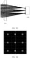
- FIG. 13 is a diagram of an optical path of an optical receiving apparatus to which no beam homogenization prism is added. After passing through a receiving prism 1301, an echo light ray is focused within a local range of a photosensitive surface of a SiPM detector with 3 ⁇ 3 pixels. Only a small part of each pixel, namely, a small quantity of cells, can receive an echo photon.
- FIG. 14 is a schematic diagram of receiving a corresponding echo photon. It can be learned that all echo photons are focus in a center of the 3 ⁇ 3 pixels.
- FIG. 15 is a diagram of an optical path of an optical receiving apparatus to which a beam homogenization prism is added.
- A3 ⁇ 3 beam homogenization prism 1503 is added before a SiPM detector 1502 with 3 ⁇ 3 pixels.
- an echo light ray is focused on a light-entrance surface of the homogenization prism.
- the echo light ray is reflected by a side wall of the beam homogenization prism for a plurality of times, the echo light ray is evenly distributed on a photosensitive surface of the 3 ⁇ 3 pixels. In other words, all cells in a pixel can receive an echo photon more evenly.
- FIG. 16 is a schematic diagram of receiving a corresponding echo photon. It can be learned that all echo photons are evenly distributed on the 3 ⁇ 3 pixels.
- the optical receiving apparatus including the beam homogenization unit may also be used in a product such as a security camera and a micro-light detection and imaging device.
- the product needs to detect a weak optical signal, and a better image may be obtained by using an array SiPM detector.
Landscapes
- Physics & Mathematics (AREA)
- Engineering & Computer Science (AREA)
- General Physics & Mathematics (AREA)
- Computer Networks & Wireless Communication (AREA)
- Radar, Positioning & Navigation (AREA)
- Remote Sensing (AREA)
- Optics & Photonics (AREA)
- Electromagnetism (AREA)
- Optical Radar Systems And Details Thereof (AREA)
- Optical Elements Other Than Lenses (AREA)
Abstract
Description
- This application claims priority to
Chinese Patent Application No. 202010619749.X, filed with the China National Intellectual Property Administration on June 30, 2020 - The disclosure relates to the light detection field, and in particular, to an optical receiving apparatus and a light detection and ranging system.
- A photodetector may be applied to many fields, for example, may be applied to a receiving apparatus in a light detection and ranging system. An operating principle of the light detection and ranging (LiDAR) system is that a laser beam at a specific frequency is emitted into a specified region, an object is encountered in a laser flying process, the laser beam is reflected on a surface of the object, and some lasers are reflected into a radar receiving apparatus to form an echo. The light detection and ranging receiving apparatus compares a received echo signal and a transmit signal, to obtain related information of the object, for example, a distance, an angle, or reflectivity.
- There are a plurality of photodetectors such as an avalanche photodiode (APD), a single photon avalanche diode (SPAD), or a silicon photomultiplier (SiPM). The silicon photomultiplier SiPM includes an avalanche diode array operating in a Geiger mode, and includes a photon counter of a plurality of pixels. One pixel includes a plurality of independent photosensitive units, referred to as a cell, and response signals of the plurality of photosensitive units are accumulated and output through a common output channel. The SiPM has characteristics such as high sensitivity, a low bias voltage, and a compact structure.
- When the SiPM is used as an optical receiving detector, because a received optical signal is converged by a receiving lens, the converged optical signal is incident on a small part of a pixel of a photosensitive surface of the SiPM, causing a small dynamic range of the detector and low detection efficiency.
- Embodiments of the disclosure provide an optical receiving apparatus and a light detection and ranging system, to increase a dynamic range of a detector and the light detection and ranging system, and improve detection efficiency. According to a first aspect, an embodiment of the disclosure provides an optical receiving apparatus, including a photodetector and a plurality of beam homogenization units. The photodetector includes a plurality of pixels, each pixel includes a plurality of cells, and the cell is configured to convert a received optical signal into an electrical signal. Each beam homogenization unit corresponds to at least one pixel of the photodetector, and is configured to diffuse a received incident light beam to a plurality of cells included in the corresponding at least one pixel. The beam homogenization unit diffuses incident light to a plurality of cells, to increase a dynamic range of the entire detector, and improve detection efficiency.
- In a possible design, the beam homogenization unit includes a beam homogenization prism; and a side wall of the beam homogenization prism is coated with a reflective coating, so that the received light beam is diffused to the plurality of cells included in the at least one pixel of the photodetector. The beam homogenization prism is used to evenly diffuse the incident light to a light-emitting surface.
- In a possible design, a length L of the beam homogenization prism meets a condition: L ≥ d/(2 ∗ tan(θ/2)), where d is a length of a short side of a light-passing cross section of the beam homogenization prism, and θ is a divergence angle existing when a light beam enters the prism. Such a dimensional characteristic enhances a diffusion effect.
- In a possible design, the beam homogenization unit further includes a diffusion sheet, disposed before a light-entrance surface of the beam homogenization prism; and the diffusion sheet is configured to diffuse and output the received incident light beam to the light-entrance surface of the beam homogenization prism. In this case, a beam homogenization effect is further improved.
- In a possible design, the beam homogenization unit further includes a microlens, disposed on a light-entrance surface of the beam homogenization unit; and the microlens is configured to converge the received incident light beam on the diffusion sheet or the light-entrance surface of the beam homogenization prism. The microlens is used to enlarge an angle of incidence of the incident light.
- In a possible design, components of the beam homogenization unit are connected through bonding by using a photosensitive adhesive. The photosensitive adhesive is used to reduce an energy loss of the incident light.
- In a possible design, the photodetector is a silicon photomultiplier SiPM. The silicon photomultiplier SiPM is used to allow the detector to have higher sensitivity.
- In a possible design, a plurality of beam homogenization units are embraced and fastened by using a mechanical part, to improve durability of the optical receiving apparatus.
- In a possible design, the beam homogenization unit corresponds to a plurality of pixels, and the plurality of beam homogenization units are a prism without internal isolation, and form a row layout, a column layout, or an irregular-shape layout, so that an application scenario of the optical receiving apparatus is more extensive.
- In a possible design, a light-emitting end face of the beam homogenization unit has a same size as a photosensitive surface in the pixel of the detector, to reduce an energy loss of the incident light.
- A second aspect, an embodiment of the disclosure provides a light detection and ranging system, including a light source, a scanner, a receiving lens, the optical receiving apparatus, and a processor. The light source is configured to output a laser beam. The scanner is configured to perform scanning in a specified region. The receiving lens is configured to converge, on the optical receiving apparatus, an echo optical signal reflected by an object. The optical receiving apparatus is configured to convert the echo optical signal into an echo electrical signal. The processor is configured to: analyze the echo electrical signal, and control the light source, the scanner, and the optical receiving apparatus. The light detection and ranging system has a large dynamic range and high detection efficiency.
- A third aspect, an embodiment of the disclosure provides a detection method, applied to the light detection and ranging system, including: outputting a control signal to a light source, to drive the light source to output a laser beam; outputting a control signal to a scanner, to drive the scanner to perform scanning in a specified mode; and receiving an echo signal output by an optical receiving apparatus, processing the echo signal, and obtaining object information corresponding to an echo. In this way, a dynamic range of detection is increased, and detection efficiency is improved.
-
-
FIG. 1 is a schematic diagram of a structure of a light detection and ranging system according to an embodiment of the disclosure; -
FIG. 2 is a schematic diagram of a photosensitive surface of a SiPM detector according to an embodiment of the disclosure; -
FIG. 3 is a schematic diagram of a relationship between a beam homogenization unit and a SiPM detector according to an embodiment of the disclosure; -
FIG. 4 is a schematic diagram in which a beam homogenization unit fits a SiPM detector according to an embodiment of the disclosure; -
FIG. 5 is a schematic diagram of a structure of a beam homogenization unit according to an embodiment of the disclosure; -
FIG. 6 is a schematic diagram of light reflection of a beam homogenization prism according to an embodiment of the disclosure; -
FIG. 7 is a schematic diagram in which beam homogenization units are embraced and fastened by using a mechanical part according to an embodiment of the disclosure; -
FIG. 8 is a schematic diagram of a scanning and detection method according to an embodiment of the disclosure; -
FIG. 9 is a schematic diagram in which beam homogenization prisms are combined according to an embodiment of the disclosure; -
FIG. 10 is a schematic three-dimensional diagram of a cylindrical microlens according to an embodiment of the disclosure; -
FIG. 11 is a schematic diagram in which an edge gap exists between photosensitive surfaces of a detector according to an embodiment of the disclosure; -
FIG. 12 is a schematic diagram of a structure of a beam homogenization unit corresponding toFIG. 11 according to an embodiment of the disclosure; -
FIG. 13 is a schematic diagram of an optical path of an optical receiving apparatus that does not include a beam homogenization prism according to an embodiment of the disclosure; -
FIG. 14 is a schematic diagram of receiving an echo photon corresponding toFIG. 13 according to an embodiment of the disclosure; -
FIG. 15 is a schematic diagram of an optical path of an optical receiving apparatus that includes a beam homogenization prism according to an embodiment of the disclosure; and -
FIG. 16 is a schematic diagram of receiving an echo photon corresponding toFIG. 15 according to an embodiment of the disclosure. - To make the objectives, technical solutions, and advantages of the disclosure clearer, the following further describes implementations of the disclosure in detail with reference to accompanying drawings.
- An embodiment of the disclosure provides an optical receiving apparatus, and a light detection and ranging system to which the optical receiving apparatus is applied. As shown in
FIG. 1 , a light detection and rangingsystem 10 includes alight source 101, ascanner 102, areceiving lens 103, anoptical receiving apparatus 104, and aprocessor 105. - The
light source 101 is configured to output a laser beam. - The
scanner 102 is configured to perform two-dimensional scanning in a specified region. - The receiving
lens 103 is configured to converge, on theoptical receiving apparatus 104, an echo optical signal reflected by anobject 11. - The
optical receiving apparatus 104 is configured to convert the echo optical signal into an echo electrical signal. Theprocessor 105 is configured to: control thelight source 101, thescanner 102, and theoptical receiving apparatus 104, and analyze the echo electrical signal to obtain a related parameter of theobject 11. After two-dimensional scanning is completed, theprocessor 105 finally obtains a point cloud image through an analysis. - The
optical receiving apparatus 104 includes a photodetector, the photodetector may be a silicon photomultiplier SiPM. The SiPM includes a plurality of pixels, and the pixels usually form a two-dimensional pixel array, for example, M * N pixels, where M and N are positive integers greater than 1. Each pixel includes a plurality of cells, and each cell is an independent photosensitive unit (cell), and is configured to convert a received optical signal into an electrical signal. Electrical signals of a plurality of cells included in one pixel are accumulated and output through a common output channel. - An example of the SiPM detector is shown in
FIG. 2 . The SiPM detector includes 6 * 4 pixels, and each pixel includes 6 * 6 pixels. To complete a point cloud image of 1440 * 900 pixels, for a SiPM detector of 6 * 4 pixels, the scanner needs to perform scanning by setting 240 angles in a horizontal direction and setting 225 angles in a vertical direction, to finally form a complete point cloud image. - The
optical receiving apparatus 104 further includes a plurality of beam homogenization units, and each beam homogenization unit corresponds to one pixel of the photodetector. The beam homogenization unit is configured to diffuse the received echo optical signal to a plurality of pixels included in a corresponding pixel. - As shown in
FIG. 3 , the optical receiving apparatus includes 6 * 4 beam homogenization units (301), and the 24 beam homogenization units respectively correspond to 6 * 4 pixels (302) of the photodetector. In an actual product, a light-emitting surface of the beam homogenization unit usually fits a photosensitive surface of the SiPM detector. -
FIG. 4 is a schematic diagram in which a beam homogenization unit fits a SiPM detector. For clarity, the photodetector in the figure includes 3 * 3 pixels, there are ninebeam homogenization units 401, and the ninebeam homogenization units 401 are in a one-to-one correspondence with the 9 pixels of theSiPM detector 402. - As shown in
FIG. 5 , a structure of the beam homogenization unit provided in this embodiment of the disclosure includes amicrolens 501, adiffusion sheet 502, and abeam homogenization prism 503. Themicrolens 501, thediffusion sheet 502, and thebeam homogenization prism 503 may be fixedly connected through bonding by using a photosensitive adhesive, to form a beam homogenization unit, as shown on a right side inFIG. 5 . - The
microlens 501 is configured to: receive an echo incident light beam, and converge the incident light beam on the diffusion sheet. The microlens may be used to enlarge a receiving numerical aperture, so that a light beam at a larger angle of incidence can enter the optical receiving apparatus. For example, a radius of spherical surface curvature of the microlens may be designed to be 1.4 mm and a thickness is 1 mm. Therefore, the receiving numerical aperture is approximately 0.25. A material of the microlens may be BK7 glass, or the like. - The
diffusion sheet 502 is configured to diffuse the received incident light beam. A divergence angle of a light beam entering the diffusion sheet through the microlens is enlarged by the diffusion sheet, to rapidly diffuse the light beam in the beam homogenization prism, and reduce a length of the beam homogenization prism. - A side wall of the
beam homogenization prism 503 is usually coated with a reflective coating, so that the light beam passing through the diffusion sheet is further diffused to a plurality of cells of a corresponding pixel of the photodetector. The beam homogenization prism has a beam homogenization function: The light beam enters the beam homogenization prism. A "photon well" is formed because the side wall of the beam homogenization prism is coated with the reflective coating. When the light beam is reflected for a plurality of times in the well, and arrives at the photosensitive surface of the photodetector SiPM, energy is evenly distributed. Because of the reflective coating, a photon cannot pass through the prism to arrive at an adjacent beam homogenization unit, to avoid crosstalk. - A light-passing cross section of the beam homogenization prism may be rectangular, and is usually square.
FIG. 6 is a schematic diagram of light reflection of a beam homogenization prism. InFIG. 6 , the length of the beam homogenization prism is L, and a side length of a cross-sectional square is d. Herein, d is usually the same size as or slightly greater than a size of a pixel of the corresponding SiPM detector, so that all light beams arrive at the photosensitive surface of the SiPM. - The length L of the beam homogenization prism may be designed based on the following condition: L ≥ d/(2 ∗ tan(θ/2)). Herein, d is a length of a shortest side of the light-passing cross section of the prism, and θ is the divergence angle existing when the light beam enters the prism. For example, in an embodiment, a size of each pixel of the detector is 1 mm * 1 mm, and a size of a light-passing surface of each beam homogenization unit is 1 mm * 1 mm. In other words, d = 1 mm.
- The side wall of the beam homogenization prism may be coated with the reflective coating, an upper end face, a lower end face, a light-entrance end face, and a light-exit end face may be coated with an anti-reflective coating, and light-passing surfaces of the microlens and the diffusion sheet may be coated with an anti-reflective coating. An operating end face of the microlens may be further polished.
- The optical receiving apparatus may include M ∗ N beam homogenization units, and the M ∗ N beam homogenization units correspond to M * N pixels of the photodetector. The beam homogenization units may be combined together in some common fastening manners, for example, may be bonded by using the photosensitive adhesive.
- The beam homogenization units may alternatively be embraced and fastened by using a mechanical part. As shown in
FIG. 7 ,3 ∗ 3 beam homogenization units are fastened by using onemechanical part 701, so that the entire optical receiving apparatus is not easily deformed, and detection performance is more stable. - A light-emitting surface of each beam homogenization unit needs to cover an effective photosensitive surface of a corresponding pixel, and a size of the light-emitting surface is the same as a size of the corresponding pixel, or is the same as a size of the effective photosensitive surface of the corresponding pixel. An exit end fits the photosensitive surface of the SiPM, to ensure that an exit does not leak light.
- When the optical receiving apparatus is assembled, the light-emitting surface of the beam homogenization unit needs to be aligned with the photosensitive surface of the pixel of the SiPM detector. A possible assembly method is as follows:
- Step 1: Fit the light-emitting end face of the beam homogenization unit and the photosensitive surface of the SiPM detector without applying an adhesive.
- Step 2: Irradiate a light-entrance port of any beam homogenization unit of the optical receiving apparatus by using a fine light beam of an operating band of the SiPM detector, monitor an output amplitude of a response signal of a corresponding pixel of the SiPM detector, adjust a location of the beam homogenization unit upward, downward, leftward, and rightward, and fasten the location of the beam homogenization unit when an output signal of the SiPM detector has a maximum amplitude.
- Step 3: Apply the photosensitive adhesive around a fitting part of the beam homogenization unit and the SiPM detector, so that the photosensitive adhesive and the SiPM detector are bonded together after the adhesive is dried. In
FIG. 7 , a location shown in 702 is the fitting part of the beam homogenization unit and the SiPM detector. - In the light detection and ranging system shown in
FIG. 1 , a light-entrance surface of theoptical receiving apparatus 104 is a light-entrance surface 703 of the beam homogenization unit shown inFIG. 7 , and needs to be placed on a focal plane of the receivinglens 103, to avoid photo crosstalk at an entrance end. - Corresponding to the light detection and ranging system shown in
FIG. 1 , an embodiment of the disclosure further provides a scanning and detection method of a light detection and ranging system. As shown inFIG. 8 , the method includes the following steps. - S1: A
processor 105 outputs a control signal to alight source 101, to drive the light source to output a laser beam. An output end of thelight source 101 may further include an emitting lens, so that a transmit light beam is shaped into a spot light beam, and then enters ascanner 102. - S2: The
processor 105 outputs a control signal, for example, information such as a scanning angle, to thescanner 102, to drive the scanner to perform scanning in a specified mode. In this way, the light beam output by the light source passes through the scanner and is transmitted to a target region. - S3: The
processor 105 receives an echo signal, performs processing, and obtains information such as an angle and a distance of an object corresponding to a current echo. The light beam output from thescanner 102 encounters an object and is reflected, to transmit an echo light beam to the light detection and ranging system. The echo light beam is converged by a receivinglens 103, and enters anoptical receiving apparatus 104. After passing through the beam homogenization unit, the light beam irradiates a photosensitive pixel of a SiPM detector. After photoelectric conversion, an echo electrical signal is output, and the processor receives the echo electrical signal for processing. Theprocessor 105 continues the process, and performs two-dimensional scanning in the target region, to form a point cloud image of the target region. - In some actual applications, a plurality of beam homogenization units may be combined to form a row layout, a column layout, or an irregular-shape layout. For example, as shown in
FIG. 9 , beam homogenization prisms of three regular cubes are combined to form a cuboid beam homogenization prism, and correspond to 1 * 3 pixels of the SiPM detector. A combination method is: combining three beam homogenization prisms with optical path isolation, to form a prism without internal isolation. Further, three spherical microlens groups shown inFIG. 9 may further form one cylindrical microlens.FIG. 10 is a stereogram of a cylindrical microlens. - An embodiment of the disclosure further provides an optical receiving apparatus, applied to an array SiPM detector having a low pixel fill factor. As shown in
FIG. 11 , an edge gap exists between photosensitive surfaces in pixels of the detector. In the figure, a size of each pixel of the detector is 1.0 mm * 1.0 mm, a size of a photosensitive surface of each pixel is 0.6 mm * 0.6 mm, a width of an edge gap between pixels is 0.4 mm, and the fill factor is 60%. Correspondingly, a structure of a beam homogenization unit is shown inFIG. 12 . In the figure, a test diagram is on a left side, and a stereogram is on a right side. The beam homogenization unit includes amicrolens 1201, adiffusion sheet 1202, abeam homogenization prism 1203, a fasteningmechanical part 1204, and aSiPM detector 1205. It can be learned from the figure that, a size of a light-emitting surface of the beam homogenization prism is reduced to a size the same as a size of the photosensitive surface of the detector. In this way, all photons received by a light-entrance end face can be introduced to the photosensitive surface in the pixel, to improve light energy utilization. It is equivalent to increase the fill factor of the detector from 60% to 100%. - The following describes an example technical effect of embodiments of the disclosure.
FIG. 13 is a diagram of an optical path of an optical receiving apparatus to which no beam homogenization prism is added. After passing through a receivingprism 1301, an echo light ray is focused within a local range of a photosensitive surface of a SiPM detector with 3 ∗ 3 pixels. Only a small part of each pixel, namely, a small quantity of cells, can receive an echo photon.FIG. 14 is a schematic diagram of receiving a corresponding echo photon. It can be learned that all echo photons are focus in a center of the 3 ∗ 3 pixels. -
FIG. 15 is a diagram of an optical path of an optical receiving apparatus to which a beam homogenization prism is added.A3 ∗ 3beam homogenization prism 1503 is added before aSiPM detector 1502 with 3 ∗ 3 pixels. After passing through a receivingprism 1501, an echo light ray is focused on a light-entrance surface of the homogenization prism. After the echo light ray is reflected by a side wall of the beam homogenization prism for a plurality of times, the echo light ray is evenly distributed on a photosensitive surface of the 3 ∗ 3 pixels. In other words, all cells in a pixel can receive an echo photon more evenly.FIG. 16 is a schematic diagram of receiving a corresponding echo photon. It can be learned that all echo photons are evenly distributed on the 3 ∗ 3 pixels. - The optical receiving apparatus including the beam homogenization unit may also be used in a product such as a security camera and a micro-light detection and imaging device. The product needs to detect a weak optical signal, and a better image may be obtained by using an array SiPM detector.
- Although the disclosure is described with reference to embodiments, in a process of implementing the disclosure that claims protection, persons skilled in the art may understand and implement another variation of the disclosed embodiments by viewing the accompanying drawings, disclosed content, and the appended claims. In the claims, "comprising" does not exclude another component or another step, and "a" or "one" does not exclude a case of multiple.
- Although the disclosure is described with reference to a specific feature and embodiments thereof, it is apparent that various modifications and combinations thereof may be made. Correspondingly, this specification and the accompanying drawings are merely example description of the disclosure defined by the appended claims, and are considered as any or all of modifications, variations, combinations or equivalents that cover the scope of the disclosure. It is clear that a person skilled in the art can make various modifications and variations to the disclosure without departing from the scope of the disclosure. The disclosure is intended to cover these modifications and variations provided that they fall within the scope of protection defined by the following claims and their equivalent technologies.
Claims (12)
- An optical receiving apparatus, comprising a photodetector and a plurality of beam homogenization units, whereinthe photodetector comprises a plurality of pixels, each pixel comprises a plurality of cells, and the cell is configured to convert a received optical signal into an electrical signal; andeach beam homogenization unit corresponds to at least one pixel of the photodetector, and is configured to diffuse a received incident light beam to a plurality of cells comprised in the corresponding at least one pixel.
- The optical receiving apparatus according to claim 1, wherein the beam homogenization unit comprises a beam homogenization prism; and
a side wall of the beam homogenization prism is coated with a reflective coating, so that the received light beam is diffused to the plurality of cells comprised in the at least one pixel of the photodetector. - The optical receiving apparatus according to claim 1, wherein a length L of the beam homogenization prism meets a condition: L ≥ d/(2 ∗ tan(θ/2)), wherein d is a length of a short side of a light-passing cross section of the beam homogenization prism, and θ is a divergence angle existing when a light beam enters the prism.
- The optical receiving apparatus according to claim 2 or 3, wherein the beam homogenization unit further comprises a diffusion sheet, disposed before a light-entrance surface of the beam homogenization prism; and the diffusion sheet is configured to diffuse and output the received incident light beam to the light-entrance surface of the beam homogenization prism.
- The optical receiving apparatus according to any one of claims 2 to 4, wherein the beam homogenization unit further comprises a microlens, disposed on a light-entrance surface of the beam homogenization unit; and the microlens is configured to converge the received incident light beam on the diffusion sheet or the light-entrance surface of the beam homogenization prism.
- The optical receiving apparatus according to any one of claims 1 to 5, wherein components of the beam homogenization unit are connected through bonding by using a photosensitive adhesive.
- The optical receiving apparatus according to any one of claims 1 to 6, wherein the photodetector is a silicon photomultiplier SiPM.
- The optical receiving apparatus according to any one of claims 1 to 7, wherein a plurality of beam homogenization units are embraced and fastened by using a mechanical part.
- The optical receiving apparatus according to any one of claims 1 to 8, wherein the beam homogenization unit corresponds to a plurality of pixels, and the plurality of beam homogenization units are a prism without internal isolation, and form a row layout, a column layout, or an irregular-shape layout.
- The optical receiving apparatus according to any one of claims 1 to 9, wherein a light-emitting surface of the beam homogenization unit has a same size as a photosensitive surface in the pixel of the photodetector.
- A light detection and ranging system, comprising a light source, a scanner, a receiving lens, the optical receiving apparatus according to claims 1 to 10, and a processor, whereinthe light source is configured to output a laser beam;the scanner is configured to perform scanning in a specified region;the receiving lens is configured to converge, on the optical receiving apparatus, an echo optical signal reflected by an object;the optical receiving apparatus is configured to convert the echo optical signal into an echo electrical signal; andthe processor is configured to: analyze the echo electrical signal, and control the light source, the scanner, and the optical receiving apparatus.
- A detection method, applied to the light detection and ranging system according to claim 11, comprising:outputting a control signal to a light source, to drive the light source to output a laser beam;outputting a control signal to a scanner, to drive the scanner to perform scanning in a specified mode; andreceiving an echo signal output by an optical receiving apparatus, processing the echo signal, and obtaining object information corresponding to an echo.
Applications Claiming Priority (2)
| Application Number | Priority Date | Filing Date | Title |
|---|---|---|---|
| CN202010619749.XA CN113945904A (en) | 2020-06-30 | 2020-06-30 | Light receiving device and laser radar system |
| PCT/CN2021/082359 WO2022001219A1 (en) | 2020-06-30 | 2021-03-23 | Light receiving device and lidar system |
Publications (3)
| Publication Number | Publication Date |
|---|---|
| EP4160261A1 true EP4160261A1 (en) | 2023-04-05 |
| EP4160261A4 EP4160261A4 (en) | 2024-02-21 |
| EP4160261B1 EP4160261B1 (en) | 2025-12-31 |
Family
ID=79317374
Family Applications (1)
| Application Number | Title | Priority Date | Filing Date |
|---|---|---|---|
| EP21833430.8A Active EP4160261B1 (en) | 2020-06-30 | 2021-03-23 | Light receiving device and lidar system |
Country Status (4)
| Country | Link |
|---|---|
| US (1) | US20230139155A1 (en) |
| EP (1) | EP4160261B1 (en) |
| CN (1) | CN113945904A (en) |
| WO (1) | WO2022001219A1 (en) |
Families Citing this family (6)
| Publication number | Priority date | Publication date | Assignee | Title |
|---|---|---|---|---|
| CN114488080A (en) * | 2022-03-11 | 2022-05-13 | 上海悠睿光学有限公司 | Light homogenizing sheet, light emitting unit for laser radar and laser radar |
| CN115316961B (en) | 2022-10-14 | 2023-02-24 | 南京诺源医疗器械有限公司 | Handheld fluorescence image probe and handheld image detector |
| CN115372950B (en) * | 2022-10-24 | 2023-01-20 | 北醒(北京)光子科技有限公司 | Silicon photomultiplier calibration device |
| CN116256729B (en) * | 2023-03-16 | 2026-01-09 | 蔚来汽车科技(安徽)有限公司 | Diffusion unit, transmission system, lidar and vehicle |
| CN116488738A (en) * | 2023-04-11 | 2023-07-25 | 浙江大学 | A SiPM optical equalization method for underwater wireless optical communication system |
| CN116593995A (en) * | 2023-06-20 | 2023-08-15 | 广州导远电子科技有限公司 | Optical signal receiving device and laser radar |
Family Cites Families (13)
| Publication number | Priority date | Publication date | Assignee | Title |
|---|---|---|---|---|
| US5357101A (en) * | 1992-09-15 | 1994-10-18 | Gap Technologies, Incorporated | Electro-optical transceiver with nonimaging concentrator |
| US20060185713A1 (en) * | 2005-02-23 | 2006-08-24 | Mook William J Jr | Solar panels with liquid superconcentrators exhibiting wide fields of view |
| US20090223555A1 (en) * | 2008-03-05 | 2009-09-10 | Stalix Llc | High Efficiency Concentrating Photovoltaic Module Method and Apparatus |
| US9318636B2 (en) * | 2012-12-11 | 2016-04-19 | International Business Machines Corporation | Secondary optic for concentrating photovoltaic device |
| CN105051522B (en) * | 2013-02-01 | 2017-10-10 | 伯乐生命医学产品有限公司 | Detection system with single-piece optics |
| CN105511083A (en) * | 2014-10-15 | 2016-04-20 | 深圳市绎立锐光科技开发有限公司 | Light homogenizing structure, manufacturing method thereof and light homogenizing system |
| JPWO2016088157A1 (en) * | 2014-12-05 | 2018-01-18 | オーエスシー株式会社 | Light receiving device for optical communication, optical communication module, and visible light communication system |
| KR102762966B1 (en) * | 2016-08-30 | 2025-02-05 | 삼성전자주식회사 | Image sensor and driving method thereof |
| CN108459328A (en) * | 2017-02-18 | 2018-08-28 | 北醒(北京)光子科技有限公司 | A kind of detection device with uniform receiving optics |
| CN206470403U (en) * | 2017-02-18 | 2017-09-05 | 北醒(北京)光子科技有限公司 | A kind of detection device with uniform receiving optics |
| CN116338711A (en) * | 2017-04-10 | 2023-06-27 | 株式会社电装 | Optical Measuring Device |
| CN111033301A (en) * | 2017-08-31 | 2020-04-17 | 深圳市大疆创新科技有限公司 | Solid state light detection and ranging (LIDAR) system |
| CN111198382B (en) * | 2018-11-16 | 2022-07-12 | 精準基因生物科技股份有限公司 | Time-of-flight distance measuring sensor and time-of-flight distance measuring method |
-
2020
- 2020-06-30 CN CN202010619749.XA patent/CN113945904A/en active Pending
-
2021
- 2021-03-23 WO PCT/CN2021/082359 patent/WO2022001219A1/en not_active Ceased
- 2021-03-23 EP EP21833430.8A patent/EP4160261B1/en active Active
-
2022
- 2022-12-28 US US18/147,242 patent/US20230139155A1/en active Pending
Also Published As
| Publication number | Publication date |
|---|---|
| EP4160261B1 (en) | 2025-12-31 |
| WO2022001219A1 (en) | 2022-01-06 |
| EP4160261A4 (en) | 2024-02-21 |
| CN113945904A (en) | 2022-01-18 |
| US20230139155A1 (en) | 2023-05-04 |
Similar Documents
| Publication | Publication Date | Title |
|---|---|---|
| US20230139155A1 (en) | Optical receiving apparatus and light detection and ranging system | |
| CN110780283B (en) | Receiving system, laser radar comprising same and echo receiving method | |
| US12461206B2 (en) | LIDAR receiver using a waveguide and an aperture | |
| JP7154230B2 (en) | Optical Imaging Transmitter with Enhanced Brightness | |
| CN113640819B (en) | Laser radar | |
| US10955531B2 (en) | Focal region optical elements for high-performance optical scanners | |
| WO2020187103A1 (en) | Prism and multi-beam lidar system | |
| CN113748358B (en) | Laser receiving device, laser receiving method and laser radar | |
| CN113227827A (en) | Laser radar and autopilot device | |
| CN210347920U (en) | Laser receiving device and laser radar system | |
| KR20230155523A (en) | laser radar | |
| CN111033301A (en) | Solid state light detection and ranging (LIDAR) system | |
| CN116559825B (en) | Laser system and laser measurement method | |
| US11378785B2 (en) | Monocentric reception arrangement | |
| CN114063088A (en) | Receiving unit of lidar, lidar and detection method thereof | |
| JPH04296642A (en) | Sample surface defect detection device | |
| CN119224786A (en) | LiDAR Systems and Vehicles | |
| CN112558038A (en) | Scanning method of laser radar | |
| CN113419247A (en) | Laser detection system | |
| US12607722B2 (en) | Optical waveguide device used in laser detection and ranging system | |
| CN113075643A (en) | Laser radar system and manufacturing method thereof | |
| US20230375672A1 (en) | Lidar device with spatial light modulators | |
| WO2025152840A1 (en) | Receiving module, radar, terminal, and vehicle end | |
| CN120871071A (en) | Area array detector, detection device, laser radar and terminal | |
| JP2026003323A (en) | Light-emitting module |
Legal Events
| Date | Code | Title | Description |
|---|---|---|---|
| STAA | Information on the status of an ep patent application or granted ep patent |
Free format text: STATUS: THE INTERNATIONAL PUBLICATION HAS BEEN MADE |
|
| PUAI | Public reference made under article 153(3) epc to a published international application that has entered the european phase |
Free format text: ORIGINAL CODE: 0009012 |
|
| STAA | Information on the status of an ep patent application or granted ep patent |
Free format text: STATUS: REQUEST FOR EXAMINATION WAS MADE |
|
| 17P | Request for examination filed |
Effective date: 20221230 |
|
| AK | Designated contracting states |
Kind code of ref document: A1 Designated state(s): AL AT BE BG CH CY CZ DE DK EE ES FI FR GB GR HR HU IE IS IT LI LT LU LV MC MK MT NL NO PL PT RO RS SE SI SK SM TR |
|
| DAV | Request for validation of the european patent (deleted) | ||
| DAX | Request for extension of the european patent (deleted) | ||
| RIC1 | Information provided on ipc code assigned before grant |
Ipc: G02B 27/09 20060101ALI20231017BHEP Ipc: G02B 19/00 20060101ALI20231017BHEP Ipc: G02B 3/00 20060101ALI20231017BHEP Ipc: G01S 7/481 20060101AFI20231017BHEP |
|
| A4 | Supplementary search report drawn up and despatched |
Effective date: 20240123 |
|
| RIC1 | Information provided on ipc code assigned before grant |
Ipc: G02B 27/09 20060101ALI20240117BHEP Ipc: G02B 19/00 20060101ALI20240117BHEP Ipc: G02B 3/00 20060101ALI20240117BHEP Ipc: G01S 7/481 20060101AFI20240117BHEP |
|
| RAP1 | Party data changed (applicant data changed or rights of an application transferred) |
Owner name: SHENZHEN YINWANG INTELLIGENTTECHNOLOGIES CO., LTD. |
|
| GRAP | Despatch of communication of intention to grant a patent |
Free format text: ORIGINAL CODE: EPIDOSNIGR1 |
|
| STAA | Information on the status of an ep patent application or granted ep patent |
Free format text: STATUS: GRANT OF PATENT IS INTENDED |
|
| INTG | Intention to grant announced |
Effective date: 20250811 |
|
| GRAS | Grant fee paid |
Free format text: ORIGINAL CODE: EPIDOSNIGR3 |
|
| GRAA | (expected) grant |
Free format text: ORIGINAL CODE: 0009210 |
|
| STAA | Information on the status of an ep patent application or granted ep patent |
Free format text: STATUS: THE PATENT HAS BEEN GRANTED |
|
| AK | Designated contracting states |
Kind code of ref document: B1 Designated state(s): AL AT BE BG CH CY CZ DE DK EE ES FI FR GB GR HR HU IE IS IT LI LT LU LV MC MK MT NL NO PL PT RO RS SE SI SK SM TR |
|
| REG | Reference to a national code |
Ref country code: CH Ref legal event code: F10 Free format text: ST27 STATUS EVENT CODE: U-0-0-F10-F00 (AS PROVIDED BY THE NATIONAL OFFICE) Effective date: 20251231 Ref country code: GB Ref legal event code: FG4D |
|
| REG | Reference to a national code |
Ref country code: DE Ref legal event code: R096 Ref document number: 602021045629 Country of ref document: DE |
|
| REG | Reference to a national code |
Ref country code: IE Ref legal event code: FG4D |
|
| PGFP | Annual fee paid to national office [announced via postgrant information from national office to epo] |
Ref country code: GB Payment date: 20260202 Year of fee payment: 6 |
|
| REG | Reference to a national code |
Ref country code: LT Ref legal event code: MG9D |
|
| PG25 | Lapsed in a contracting state [announced via postgrant information from national office to epo] |
Ref country code: NO Free format text: LAPSE BECAUSE OF FAILURE TO SUBMIT A TRANSLATION OF THE DESCRIPTION OR TO PAY THE FEE WITHIN THE PRESCRIBED TIME-LIMIT Effective date: 20260331 |
|
| PGFP | Annual fee paid to national office [announced via postgrant information from national office to epo] |
Ref country code: DE Payment date: 20260204 Year of fee payment: 6 |
|
| PG25 | Lapsed in a contracting state [announced via postgrant information from national office to epo] |
Ref country code: HR Free format text: LAPSE BECAUSE OF FAILURE TO SUBMIT A TRANSLATION OF THE DESCRIPTION OR TO PAY THE FEE WITHIN THE PRESCRIBED TIME-LIMIT Effective date: 20251231 Ref country code: FI Free format text: LAPSE BECAUSE OF FAILURE TO SUBMIT A TRANSLATION OF THE DESCRIPTION OR TO PAY THE FEE WITHIN THE PRESCRIBED TIME-LIMIT Effective date: 20251231 |
|
| PG25 | Lapsed in a contracting state [announced via postgrant information from national office to epo] |
Ref country code: RS Free format text: LAPSE BECAUSE OF FAILURE TO SUBMIT A TRANSLATION OF THE DESCRIPTION OR TO PAY THE FEE WITHIN THE PRESCRIBED TIME-LIMIT Effective date: 20260331 |
|
| PGFP | Annual fee paid to national office [announced via postgrant information from national office to epo] |
Ref country code: FR Payment date: 20260209 Year of fee payment: 6 |
|
| PG25 | Lapsed in a contracting state [announced via postgrant information from national office to epo] |
Ref country code: LV Free format text: LAPSE BECAUSE OF FAILURE TO SUBMIT A TRANSLATION OF THE DESCRIPTION OR TO PAY THE FEE WITHIN THE PRESCRIBED TIME-LIMIT Effective date: 20251231 |
|
| PG25 | Lapsed in a contracting state [announced via postgrant information from national office to epo] |
Ref country code: BG Free format text: LAPSE BECAUSE OF FAILURE TO SUBMIT A TRANSLATION OF THE DESCRIPTION OR TO PAY THE FEE WITHIN THE PRESCRIBED TIME-LIMIT Effective date: 20251231 |
|
| REG | Reference to a national code |
Ref country code: NL Ref legal event code: MP Effective date: 20251231 |
|
| REG | Reference to a national code |
Ref country code: CH Ref legal event code: W10 Free format text: ST27 STATUS EVENT CODE: U-0-0-W10-W00 (AS PROVIDED BY THE NATIONAL OFFICE) Effective date: 20260507 |