EP4157091B1 - Biometric sensor integrated with electronic display of a wearable device - Google Patents
Biometric sensor integrated with electronic display of a wearable device Download PDFInfo
- Publication number
- EP4157091B1 EP4157091B1 EP21756095.2A EP21756095A EP4157091B1 EP 4157091 B1 EP4157091 B1 EP 4157091B1 EP 21756095 A EP21756095 A EP 21756095A EP 4157091 B1 EP4157091 B1 EP 4157091B1
- Authority
- EP
- European Patent Office
- Prior art keywords
- biometric sensor
- double
- computing device
- circuit board
- printed circuit
- Prior art date
- Legal status (The legal status is an assumption and is not a legal conclusion. Google has not performed a legal analysis and makes no representation as to the accuracy of the status listed.)
- Active
Links
Images







Classifications
-
- G—PHYSICS
- G06—COMPUTING OR CALCULATING; COUNTING
- G06F—ELECTRIC DIGITAL DATA PROCESSING
- G06F1/00—Details not covered by groups G06F3/00 - G06F13/00 and G06F21/00
- G06F1/16—Constructional details or arrangements
- G06F1/1613—Constructional details or arrangements for portable computers
- G06F1/163—Wearable computers, e.g. on a belt
-
- A—HUMAN NECESSITIES
- A61—MEDICAL OR VETERINARY SCIENCE; HYGIENE
- A61B—DIAGNOSIS; SURGERY; IDENTIFICATION
- A61B5/00—Measuring for diagnostic purposes; Identification of persons
- A61B5/02—Detecting, measuring or recording for evaluating the cardiovascular system, e.g. pulse, heart rate, blood pressure or blood flow
- A61B5/024—Measuring pulse rate or heart rate
- A61B5/02438—Measuring pulse rate or heart rate with portable devices, e.g. worn by the patient
-
- A—HUMAN NECESSITIES
- A61—MEDICAL OR VETERINARY SCIENCE; HYGIENE
- A61B—DIAGNOSIS; SURGERY; IDENTIFICATION
- A61B5/00—Measuring for diagnostic purposes; Identification of persons
- A61B5/02—Detecting, measuring or recording for evaluating the cardiovascular system, e.g. pulse, heart rate, blood pressure or blood flow
- A61B5/024—Measuring pulse rate or heart rate
- A61B5/02444—Details of sensor
-
- A—HUMAN NECESSITIES
- A61—MEDICAL OR VETERINARY SCIENCE; HYGIENE
- A61B—DIAGNOSIS; SURGERY; IDENTIFICATION
- A61B5/00—Measuring for diagnostic purposes; Identification of persons
- A61B5/02—Detecting, measuring or recording for evaluating the cardiovascular system, e.g. pulse, heart rate, blood pressure or blood flow
- A61B5/024—Measuring pulse rate or heart rate
- A61B5/0245—Measuring pulse rate or heart rate by using sensing means generating electric signals, i.e. ECG signals
-
- A—HUMAN NECESSITIES
- A61—MEDICAL OR VETERINARY SCIENCE; HYGIENE
- A61B—DIAGNOSIS; SURGERY; IDENTIFICATION
- A61B5/00—Measuring for diagnostic purposes; Identification of persons
- A61B5/05—Detecting, measuring or recording for diagnosis by means of electric currents or magnetic fields; Measuring using microwaves or radio waves
- A61B5/053—Measuring electrical impedance or conductance of a portion of the body
- A61B5/0531—Measuring skin impedance
-
- A—HUMAN NECESSITIES
- A61—MEDICAL OR VETERINARY SCIENCE; HYGIENE
- A61B—DIAGNOSIS; SURGERY; IDENTIFICATION
- A61B5/00—Measuring for diagnostic purposes; Identification of persons
- A61B5/24—Detecting, measuring or recording bioelectric or biomagnetic signals of the body or parts thereof
- A61B5/25—Bioelectric electrodes therefor
- A61B5/251—Means for maintaining electrode contact with the body
- A61B5/256—Wearable electrodes, e.g. having straps or bands
-
- A—HUMAN NECESSITIES
- A61—MEDICAL OR VETERINARY SCIENCE; HYGIENE
- A61B—DIAGNOSIS; SURGERY; IDENTIFICATION
- A61B5/00—Measuring for diagnostic purposes; Identification of persons
- A61B5/24—Detecting, measuring or recording bioelectric or biomagnetic signals of the body or parts thereof
- A61B5/25—Bioelectric electrodes therefor
- A61B5/279—Bioelectric electrodes therefor specially adapted for particular uses
- A61B5/28—Bioelectric electrodes therefor specially adapted for particular uses for electrocardiography [ECG]
-
- A—HUMAN NECESSITIES
- A61—MEDICAL OR VETERINARY SCIENCE; HYGIENE
- A61B—DIAGNOSIS; SURGERY; IDENTIFICATION
- A61B5/00—Measuring for diagnostic purposes; Identification of persons
- A61B5/68—Arrangements of detecting, measuring or recording means, e.g. sensors, in relation to patient
- A61B5/6801—Arrangements of detecting, measuring or recording means, e.g. sensors, in relation to patient specially adapted to be attached to or worn on the body surface
- A61B5/6802—Sensor mounted on worn items
- A61B5/681—Wristwatch-type devices
-
- G—PHYSICS
- G06—COMPUTING OR CALCULATING; COUNTING
- G06F—ELECTRIC DIGITAL DATA PROCESSING
- G06F1/00—Details not covered by groups G06F3/00 - G06F13/00 and G06F21/00
- G06F1/16—Constructional details or arrangements
- G06F1/1613—Constructional details or arrangements for portable computers
- G06F1/1633—Constructional details or arrangements of portable computers not specific to the type of enclosures covered by groups G06F1/1615 - G06F1/1626
- G06F1/1637—Details related to the display arrangement, including those related to the mounting of the display in the housing
- G06F1/1643—Details related to the display arrangement, including those related to the mounting of the display in the housing the display being associated to a digitizer, e.g. laptops that can be used as penpads
-
- G—PHYSICS
- G06—COMPUTING OR CALCULATING; COUNTING
- G06F—ELECTRIC DIGITAL DATA PROCESSING
- G06F1/00—Details not covered by groups G06F3/00 - G06F13/00 and G06F21/00
- G06F1/16—Constructional details or arrangements
- G06F1/1613—Constructional details or arrangements for portable computers
- G06F1/1633—Constructional details or arrangements of portable computers not specific to the type of enclosures covered by groups G06F1/1615 - G06F1/1626
- G06F1/1656—Details related to functional adaptations of the enclosure, e.g. to provide protection against EMI, shock, water, or to host detachable peripherals like a mouse or removable expansions units like PCMCIA cards, or to provide access to internal components for maintenance or to removable storage supports like CDs or DVDs, or to mechanically mount accessories
-
- G—PHYSICS
- G06—COMPUTING OR CALCULATING; COUNTING
- G06F—ELECTRIC DIGITAL DATA PROCESSING
- G06F1/00—Details not covered by groups G06F3/00 - G06F13/00 and G06F21/00
- G06F1/16—Constructional details or arrangements
- G06F1/1613—Constructional details or arrangements for portable computers
- G06F1/1633—Constructional details or arrangements of portable computers not specific to the type of enclosures covered by groups G06F1/1615 - G06F1/1626
- G06F1/1656—Details related to functional adaptations of the enclosure, e.g. to provide protection against EMI, shock, water, or to host detachable peripherals like a mouse or removable expansions units like PCMCIA cards, or to provide access to internal components for maintenance or to removable storage supports like CDs or DVDs, or to mechanically mount accessories
- G06F1/1658—Details related to functional adaptations of the enclosure, e.g. to provide protection against EMI, shock, water, or to host detachable peripherals like a mouse or removable expansions units like PCMCIA cards, or to provide access to internal components for maintenance or to removable storage supports like CDs or DVDs, or to mechanically mount accessories related to the mounting of internal components, e.g. disc drive or any other functional module
-
- G—PHYSICS
- G06—COMPUTING OR CALCULATING; COUNTING
- G06F—ELECTRIC DIGITAL DATA PROCESSING
- G06F1/00—Details not covered by groups G06F3/00 - G06F13/00 and G06F21/00
- G06F1/16—Constructional details or arrangements
- G06F1/1613—Constructional details or arrangements for portable computers
- G06F1/1633—Constructional details or arrangements of portable computers not specific to the type of enclosures covered by groups G06F1/1615 - G06F1/1626
- G06F1/1684—Constructional details or arrangements related to integrated I/O peripherals not covered by groups G06F1/1635 - G06F1/1675
-
- A—HUMAN NECESSITIES
- A61—MEDICAL OR VETERINARY SCIENCE; HYGIENE
- A61B—DIAGNOSIS; SURGERY; IDENTIFICATION
- A61B2503/00—Evaluating a particular growth phase or type of persons or animals
- A61B2503/10—Athletes
-
- A—HUMAN NECESSITIES
- A61—MEDICAL OR VETERINARY SCIENCE; HYGIENE
- A61B—DIAGNOSIS; SURGERY; IDENTIFICATION
- A61B2560/00—Constructional details of operational features of apparatus; Accessories for medical measuring apparatus
- A61B2560/04—Constructional details of apparatus
- A61B2560/0462—Apparatus with built-in sensors
- A61B2560/0468—Built-in electrodes
-
- A—HUMAN NECESSITIES
- A61—MEDICAL OR VETERINARY SCIENCE; HYGIENE
- A61B—DIAGNOSIS; SURGERY; IDENTIFICATION
- A61B2562/00—Details of sensors; Constructional details of sensor housings or probes; Accessories for sensors
- A61B2562/02—Details of sensors specially adapted for in-vivo measurements
- A61B2562/0209—Special features of electrodes classified in A61B5/24, A61B5/25, A61B5/283, A61B5/291, A61B5/296, A61B5/053
-
- A—HUMAN NECESSITIES
- A61—MEDICAL OR VETERINARY SCIENCE; HYGIENE
- A61B—DIAGNOSIS; SURGERY; IDENTIFICATION
- A61B2562/00—Details of sensors; Constructional details of sensor housings or probes; Accessories for sensors
- A61B2562/12—Manufacturing methods specially adapted for producing sensors for in-vivo measurements
- A61B2562/125—Manufacturing methods specially adapted for producing sensors for in-vivo measurements characterised by the manufacture of electrodes
-
- A—HUMAN NECESSITIES
- A61—MEDICAL OR VETERINARY SCIENCE; HYGIENE
- A61B—DIAGNOSIS; SURGERY; IDENTIFICATION
- A61B2562/00—Details of sensors; Constructional details of sensor housings or probes; Accessories for sensors
- A61B2562/16—Details of sensor housings or probes; Details of structural supports for sensors
-
- A—HUMAN NECESSITIES
- A61—MEDICAL OR VETERINARY SCIENCE; HYGIENE
- A61B—DIAGNOSIS; SURGERY; IDENTIFICATION
- A61B2562/00—Details of sensors; Constructional details of sensor housings or probes; Accessories for sensors
- A61B2562/16—Details of sensor housings or probes; Details of structural supports for sensors
- A61B2562/166—Details of sensor housings or probes; Details of structural supports for sensors the sensor is mounted on a specially adapted printed circuit board
-
- A—HUMAN NECESSITIES
- A61—MEDICAL OR VETERINARY SCIENCE; HYGIENE
- A61B—DIAGNOSIS; SURGERY; IDENTIFICATION
- A61B2562/00—Details of sensors; Constructional details of sensor housings or probes; Accessories for sensors
- A61B2562/22—Arrangements of medical sensors with cables or leads; Connectors or couplings specifically adapted for medical sensors
- A61B2562/225—Connectors or couplings
- A61B2562/227—Sensors with electrical connectors
Definitions
- the present disclosure relates generally to wearable computing devices, and more particularly, to a biometric sensor electrode integrated in the top surface of the covering of a wearable computing device, thereby providing increased surface area and improved signal quality of the sensor.
- biometric monitoring devices may collect, derive, and/or provide one or more of the following types of information: heart rate, calorie burn, floors climbed and/or descended, location and/or heading, elevation, ambulatory speed and/or distance traveled, etc.
- the front or top surface is typically occupied by a large electronic display, often covered with an optically clear covering constructed of certain materials (such as glass, polycarbonate, acrylic, etc.). This covering often requires a seal around its perimeter, making the electronic display covering larger than the active region of the electronic display itself.
- the present disclosure is related to a biometric sensor electrode integrated in the top surface of the covering of such wearable computing devices, thereby providing increased surface area and improved signal quality of the sensor.
- the biometric sensor electrode integrated in the top surface of the covering of such wearable computing devices, thereby providing increased surface area and improved signal quality of the sensor.
- the wearable computing device includes an outer covering defining an outer-most top surface and an outer perimeter and an internal volume defined, at least in part, by an inner surface of the outer covering.
- the wearable computing device also includes an electronic display and an electronic display module connector arranged within the internal volume.
- the wearable computing device includes at least one biometric sensor electrode positioned on the outer-most top surface of the outer covering and wrapping around one or more side edges of the outer covering to the internal volume.
- the wearable computing device includes a printed circuit board arranged within the internal volume.
- the wearable computing device includes a conductive component electrically connecting the biometric sensor electrode(s) to the printed circuit board through the electronic display module connector. Further, the conductive component defines a low-resistance path.
- Another example aspect of the present disclosure is directed to a method of assembling a wearable computing device.
- the method includes providing an outer covering defining an outer-most top surface and an outer perimeter, an inner surface of the outer covering defining an internal volume.
- the method also includes positioning a first portion of at least one biometric sensor electrode on the outer-most top surface of the outer covering and wrapping a second portion of the at least one biometric sensor electrode around one or more side edges of the outer covering such that the second portion is within the internal volume.
- the method includes placing an electronic display and an electronic display module connector within the internal volume.
- the method includes arranging a printed circuit board within the internal volume adjacent to the electronic display.
- the method includes electrically connecting the biometric sensor electrode(s) to the printed circuit board through the electronic display module connector via at least one conductive component. Further, the conductive component(s) defines a low-resistance path.
- the front or top surface is typically occupied by a large electronic display, often covered with an optically clear covering constructed of certain materials (such as glass, polycarbonate, acrylic, etc.).
- This covering often requires a seal around its perimeter, making the electronic display covering larger than the active region of the electronic display itself.
- the present disclosure is related to a biometric sensor electrode integrated in the top surface of the covering on a wearable computing device, thereby providing increased surface area and improved signal quality of the sensor.
- the user is able to access the sensor in a more ergonomic manner, allowing the user to make contact with a variety of extremities (palm, fingers, leg, etc.) without requiring high dexterity on a small surface.
- the present disclosure is also directed to an improved conductive component between the biometric sensor electrode and the main circuit of the wearable computing device.
- the present disclosure provides for electrically connecting an efficient and effective conductive component to a printed or flexible circuit board through the electronic display module and into the main circuit of the wearable computing device.
- the improved conductive component of the present disclosure has a low feed-thru electrical resistance and does not require extra space.
- the integrated biometric sensor electrode allows for an easy assembly process without increasing costs or reducing reliability.
- a direct/indirect connection may be used with conductive foam and an adhesive (such as anisotropic conductive film (ACF) and silver epoxy).
- an adhesive such as anisotropic conductive film (ACF) and silver epoxy.
- PVD physical vapor deposition
- a low-resistance conductive foam is placed between the sensor metal bottom and the PVD contact pads to connect the biometric sensor electrode to PVD contact pad(s).
- the PVD contact pad(s) on the top surface is connected to a flexible printed circuit (FBC) through the electronic display module connector.
- the FBC is bonded on the top surface using an adhesive, such as ACF, by conventional FPC bonding processes.
- the electronic display module connector is secured to the main device body, where the main circuit is located.
- FIG. 1 illustrates a perspective view of a wearable computing device 100 according to the present disclosure.
- the wearable computing device 100 may be worn on a person's forearm like a wristwatch.
- the wearable computing device 100 has a housing 102 that contains the electronics associated with the wearable computing device 100.
- the wearable computing device 100 includes one or more buttons 104 and an electronic display 106 that is accessible/visible through the housing 102.
- the button(s) 404 may be implemented to provide a mechanism to activate a heart rate sensor to collect heart rate data.
- the electronic display 106 may cover an electronics package 110 (also referred to herein as an electronic display module connector), which is also housed with the housing 102.
- an electronics package 110 also referred to herein as an electronic display module connector
- a wristband 108 may be integrated with the housing 102.
- FIGS. 2-7 various views of the housing 102 of the wearable computing device 100 according to the present disclosure are illustrated.
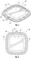
- FIG. 2 illustrates a top view of one embodiment of the housing 102 according to the present disclosure
- FIG. 3 illustrates a side view of one embodiment of the housing 102 according to the present disclosure
- FIG. 4 illustrates an exploded side view of one embodiment of the housing 102 according to the present disclosure
- FIG. 5 illustrates a transparent, perspective view of one embodiment of the housing 102 according to the present disclosure
- FIG. 6 illustrates a transparent, top view of one embodiment of the housing 102 according to the present disclosure
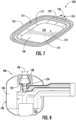
- FIG. 7 illustrates a transparent, perspective view of one embodiment of the housing 102 according to the present disclosure
- FIG. 8 illustrates a rear view of one embodiment of the electronics package 110 within the housing 102 according to the present disclosure.
- the housing 102 includes an outer covering 112 defining an outer-most top surface 114 and an outer perimeter 116.
- the outer covering 112 may be constructed of glass, polycarbonate, acrylic, or similar.
- an internal volume 118 is defined, at least in part, by an inner surface 120 of the outer covering 112.
- the wearable computing device 100 may also include a seal 115 arranged along the outer perimeter 116 of the outer covering 112.
- the internal volume 118 is defined by the inner surface 120 of the outer covering 112 and an inner edge 117 of the seal 115.
- the electronic display 106 and the electronic display module connector 110 may be arranged within the internal volume 118, as further described herein.
- the wearable computing device 100 further includes at least one biometric sensor electrode, such as a first biometric sensor electrode 122 and a second biometric sensor electrode 124, positioned on the outer-most top surface 114 of the outer covering 112 and wrapping around one or more side edges of the outer covering 112 to the internal volume 118 (see e.g., FIG. 7 ).
- the wearable computing device 100 may include two sensor electrodes 122, 124 placed in a pair. In such embodiment, the two sensor electrodes 122, 124 may have an overlapped space over a display dimension.
- the wearable computing device 100 includes a printed circuit board 128 arranged within the internal volume 118, i.e., on a rear side of the electronics display 106.
- the first and second biometric sensor electrodes 122, 124 are arranged on opposite sides of the printed circuit board 128.
- the first and second biometric sensor electrodes 122, 124 are arranged on the same side of the printed circuit board 128.
- the biometric sensor electrode(s) 122, 124 described herein may each include a physical vapor deposition (PVD) sensor pad.
- the biometric sensor electrode(s) 122, 124 described herein may include an electrocardiogram (ECG) sensor, an electrodermal activity (EDA) sensor, or any other suitable sensor type.
- ECG electrocardiogram
- EDA electrodermal activity
- the biometric sensor electrode(s) 122, 124 described herein may be connected through inter-media materials to the electronic display module connector 110, which may include a computing system configured to operate the wearable computing device 100.
- the electronic display module connector 110 may include a computing system configured to operate the wearable computing device 100.
- FIG. 9 a block diagram of an example computing system 150 according to example embodiments of the present disclosure is illustrated.
- the computing system 150 includes a user computing device 152, a server computing system 160, and a training computing system 170 that are communicatively coupled over a network 180.
- components of the user computing device 152 may be part of the wearable computing device 100.
- the user computing device 152 includes one or more processors 154 and a memory 155.
- the one or more processors 154 can be any suitable processing device (e.g., a processor core, a microprocessor, an ASIC, an FPGA, a controller, a microcontroller, etc.) and can be one processor or a plurality of processors that are operatively connected.
- the memory 155 can include one or more non-transitory computer-readable storage media, such as RAM, ROM, EEPROM, EPROM, flash memory devices, magnetic disks, etc., and combinations thereof.
- the memory 155 can store data 156 and instructions 157 which are executed by the processor 154 to cause the user computing device 152 to perform operations.
- the model(s) 158 can be received from the server computing system 160 over the network 180, stored in the user computing device memory 155, and then used or otherwise implemented by the processor(s) 154. Additionally, or alternatively, one or more models 168 can be included in or otherwise stored and implemented by the server computing system 160 that communicates with the user computing device 152 according to a client-server relationship. Thus, the model(s) 158 can be stored and implemented at the user computing device 152 and/or the model(s) 168 can be stored and implemented at the server computing system 160.
- the user computing device 152 can also include one or more user input components 159 that receives user input.
- the user input component 159 can be a touch-sensitive component (e.g., a touch-sensitive display screen or a touch pad) that is sensitive to the touch of a user input object (e.g., a finger or a stylus).
- the touch-sensitive component can serve to implement a virtual keyboard.
- Other example user input components include a microphone, a traditional keyboard, or other means by which a user can provide user input.
- the server computing system 160 can be any type of computing device, such as, for example, a personal computing device (e.g., laptop or desktop), a mobile computing device (e.g., smartphone or tablet), a gaming console or controller, a wearable computing device, an embedded computing device, or any other type of computing device. Further, as shown, the server computing system 160 includes one or more processors 162 and a memory 164.
- the processor(s) 162 can be any suitable processing device (e.g., a processor core, a microprocessor, an ASIC, an FPGA, a controller, a microcontroller, etc.) and can be one processor or a plurality of processors that are operatively connected.
- the memory 164 can include one or more non-transitory computer-readable storage media, such as RAM, ROM, EEPROM, EPROM, flash memory devices, magnetic disks, etc., and combinations thereof.
- the memory 164 can store data 165 and instructions 166 which are executed by the processor 162 to cause the server computing system 160 to perform operations.
- the server computing system 160 includes or is otherwise implemented by one or more server computing devices. In instances in which the server computing system 160 includes plural server computing devices, such server computing devices can operate according to sequential computing architectures, parallel computing architectures, or some combination thereof.
- the server computing system 160 can store or otherwise include one or more models 168.
- the model(s) 168 can be or can otherwise include various machine-learned models.
- Example machine-learned models include neural networks or other multi-layer non-linear models.
- Example neural networks include feed forward neural networks, deep neural networks, recurrent neural networks, and convolutional neural networks.
- the user computing device 152 and/or the server computing system 160 can train the models 158 and/or 168 via interaction with the training computing system 170 that is communicatively coupled over the network 180.
- the training computing system 170 can be separate from the server computing system 160 or can be a portion of the server computing system 160.
- the training computing system 170 includes one or more processors 172 and a memory 174.
- the processor(s) 172 can be any suitable processing device (e.g., a processor core, a microprocessor, an ASIC, an FPGA, a controller, a microcontroller, etc.) and can be one processor or a plurality of processors that are operatively connected.
- the memory 174 can include one or more non-transitory computer-readable storage media, such as RAM, ROM, EEPROM, EPROM, flash memory devices, magnetic disks, etc., and combinations thereof.
- the memory 174 can store data 175 and instructions 176 which are executed by the processor 172 to cause the training computing system 170 to perform operations.
- the training computing system 170 includes or is otherwise implemented by one or more server computing devices.
- the training computing system 170 can also include a model trainer 177 that trains the machine-learned models 158 and/or 168 stored at the user computing device 152 and/or the server computing system 160 using various training or learning techniques.
- the model trainer 177 can train the models 158 and/or 168 based on a set of training data 178.
- the model trainer 177 includes computer logic utilized to provide desired functionality.
- the model trainer 177 can be implemented in hardware, firmware, and/or software controlling a general purpose processor.
- the model trainer 177 includes program files stored on a storage device, loaded into a memory and executed by one or more processors.
- the model trainer 177 includes one or more sets of computer-executable instructions that are stored in a tangible computer-readable storage medium such as RAM, hard disk, or optical or magnetic media.
- the network 180 can be any type of communications network, such as a local area network (e.g., intranet), wide area network (e.g., Internet), or some combination thereof and can include any number of wired or wireless links.
- communication over the network 180 can be carried via any type of wired and/or wireless connection, using a wide variety of communication protocols (e.g., TCP/IP, HTTP, SMTP, FTP), encodings or formats (e.g., HTML, XML), and/or protection schemes (e.g., VPN, secure HTTP, SSL).
- the wearable computing device 100 of the present disclosure further includes a conductive component 130 electrically connecting the biometric sensor electrode(s) 122, 124 to the printed circuit board 128 through the electronic display module connector 110.
- the conductive component 130 described herein provides a low-resistance path (e.g., on the order of less than about 50 Ohms, in particular less than 10 Ohms).
- the conductive component 130 is double-side conductive foam 132 or tape.
- the double-side conductive foam 132 or tape may be sandwiched between a bottom surface 138 of the outer covering 112 and a top surface 140 of the electronic display 106.
- the signal path as indicated by arrows 123, travels through the electronic display 106 first and then through the printed circuit board 128.
- the electronic display 106 can be connected through the printed circuit board 128 by anisotropic conductive film (ACF) bonding.
- ACF anisotropic conductive film
- ACF bonding generally refers to a lead-free and environmentally friendly adhesive interconnect film system or paste that can be used to make electrical and mechanical connections.
- conductive line(s) 142 connected to the biometric sensor electrode(s) 122, 124 and the conductive component 130 are connected to the printed circuit board 128 to deliver the sensing signal to the electronics package 110.
- the double-side conductive foam 132 or tape may be placed on a top surface 121 of the printed circuit board 128.
- the electronic display 106 becomes part of the printed circuit board 128 (i.e., its top surface).
- the double-side conductive foam 132 or tape is configured to sit on the top surface 121 of the printed circuit board 128 (e.g., on the wing side top surface of the electronic display 106).
- the signal path as indicated by arrows 125, travels by the electronic display 106 and directly through the printed circuit board 128.
- the conductive component 130 is double-side conductive tape 134 or film.
- the conductive tape 134 or film may be applied directly to the biometric sensor electrode(s) 122, 124 to electrically connect the biometric sensor electrode(s) 122, 124 to the printed circuit board 128.
- the biometric sensor electrode(s) 122, 124 wrap around the side edge of the outer covering 112 to the internal volume 118 such that a first end of the conductive tape 134 or film can be secured to an end of the biometric sensor electrode(s) 122, 124 and an opposing end of the conductive tape 134 or film can be secured directly to the printed circuit board 128 (or to a conductive component in direct contact with the printed circuit board 128).
- the conductive component 130 may include separate conductive tapes or a single conductive tape with two conductive lines.
- the conductive component 130 is ACF (anisotropic conductive film or paste) bonding 135.
- the ACF bonding 135 can be applied directly to the biometric sensor electrode(s) 122, 124 to electrically connect the biometric sensor electrode(s) 122, 124 to the printed circuit board 128.
- the ACF bonding 135 can be used alone or in combination with the conductive tape 134 or film to provide additional support.
- the ACF bonding 135 can be connected to the biometric sensor electrode(s) 122, 124, which are located on a hard glass surface.
- the electronics display 106 can then be laminated on top of the ACF bonding 135.
- the ACF bonding 135 can be connected to the printed circuit board 128 or any suitable location that can ultimately be electrically connected to the printed circuit board 128. Such a connection can be completed using, for example, soldering, connectors, springs, fasteners, or similar.
- the conductive component 130 is a conductive adhesive 136 through direct contact, such as, for example, silver epoxy.
- the conductive component 130 may be single-side conductive tape, single-side conductive foam, anisotropic conductive film, or combinations thereof. In further embodiments, any suitable connection is possible to connect such components together to define the desired low-resistance path.
- the wearable computing device 100 may further include a contact pad 144 arranged between the double-side conductive foam 130, 132 or tape and the top surface 140 of the electronic display 106.
- the contact pad 144 may be a thin metal film.
- the printed circuit board 128 is electrically coupled to an edge of the contact pad 144, e.g., through conductive line(s) 142.
- the printed circuit board 128 may be arranged adjacent to the contact pad 144 and may be electrically connected to a bottom surface of the contact pad 144 such that the conductive line(s) 142 can be omitted.
- the wearable computing device may be any suitable wearable computing device such as the wearable computing device 100 described herein with reference to FIGS. 1-23 .
- the method 200 is described herein with reference to the wearable computing device 100 of FIGS. 1-24 .
- the disclosed method 200 may be implemented with any other suitable wearable computing device having any other suitable configurations.
- FIG. 24 depicts steps performed in a particular order for purposes of illustration and discussion, the methods discussed herein are not limited to any particular order or arrangement.
- One skilled in the art, using the disclosures provided herein, will appreciate that various steps of the methods disclosed herein can be omitted, rearranged, combined, and/or adapted in various ways without deviating from the scope of the present disclosure.
- the method 200 includes providing an outer covering defining an outer-most top surface and an outer perimeter, an inner surface of the outer covering defining an internal volume.
- FIGS. 2-7 generally illustrate an embodiment of the outer covering 112 according to the present disclosure.
- the method 200 includes positioning a first portion of at least one biometric sensor electrode on the outer-most top surface of the outer covering and wrapping a second portion of the at least one biometric sensor electrode around one or more side edges of the outer covering such that the second portion is within the internal volume.
- FIGS. 2-7 generally illustrate an embodiment of a first portion of the biometric sensor electrodes 122, 124 on the outer-most top surface 114 of the outer covering 112.
- a second portion of the biometric sensor electrodes 122, 124 wrap around one or more side edges of the outer covering 112 such that the second portion is within the internal volume 118 of the wearable computing device 100 according to the present disclosure.
- the method 200 includes placing an electronic display and an electronic display module connector within the internal volume. As shown at (208), the method 200 includes arranging a printed circuit board within the internal volume adjacent to the electronic display.
- the method 200 includes electrically connecting the biometric sensor electrode(s) to the printed circuit board through the electronic display module connector via at least one conductive component.
- the conductive component(s) defines a low-resistance path.
- electrically connecting the biometric sensor electrode(s) 122, 124 to the printed circuit board 128 through the electronic display module connector 110 includes placing the conductive component(s) 130 between the bottom surface 138 of the outer covering 112 and a top surface of 119 the electronic display 106.
- FIG. 10-14 electrically connecting the biometric sensor electrode(s) 122, 124 to the printed circuit board 128 through the electronic display module connector 110 includes placing the conductive component(s) 130 between the bottom surface 138 of the outer covering 112 and a top surface of 119 the electronic display 106.
- electrically connecting the biometric sensor electrode(s) 122, 124 to the printed circuit board 128 through the electronic display module connector 110 includes placing the conductive component(s) 130 on a top surface 121 of the printed circuit board 128.
- the conductive component(s) 130 may be double-side conductive tape, double-side conductive foam, single-side conductive tape, single-side conductive foam, conductive adhesive, anisotropic conductive film, or combinations thereof.
- the method 200 may include laminating the outer covering 112, the double-side conductive tape or the double-side conductive foam 132, and the biometric sensor electrode(s) 122, 124 together.
- the technology discussed herein makes reference to servers, databases, software applications, and other computer-based systems, as well as actions taken and information sent to and from such systems.
- the inherent flexibility of computer-based systems allows for a great variety of possible configurations, combinations, and divisions of tasks and functionality between and among components.
- processes discussed herein can be implemented using a single device or component or multiple devices or components working in combination.
- Databases and applications can be implemented on a single system or distributed across multiple systems. Distributed components can operate sequentially or in parallel.
Landscapes
- Health & Medical Sciences (AREA)
- Engineering & Computer Science (AREA)
- Life Sciences & Earth Sciences (AREA)
- Physics & Mathematics (AREA)
- Computer Hardware Design (AREA)
- Theoretical Computer Science (AREA)
- Animal Behavior & Ethology (AREA)
- Veterinary Medicine (AREA)
- Biophysics (AREA)
- Biomedical Technology (AREA)
- Heart & Thoracic Surgery (AREA)
- Medical Informatics (AREA)
- Molecular Biology (AREA)
- Surgery (AREA)
- Pathology (AREA)
- General Health & Medical Sciences (AREA)
- Public Health (AREA)
- Cardiology (AREA)
- General Engineering & Computer Science (AREA)
- Human Computer Interaction (AREA)
- General Physics & Mathematics (AREA)
- Physiology (AREA)
- Radiology & Medical Imaging (AREA)
- Nuclear Medicine, Radiotherapy & Molecular Imaging (AREA)
- Dermatology (AREA)
- Signal Processing (AREA)
- Measurement And Recording Of Electrical Phenomena And Electrical Characteristics Of The Living Body (AREA)
- User Interface Of Digital Computer (AREA)
Description
- The present disclosure relates generally to wearable computing devices, and more particularly, to a biometric sensor electrode integrated in the top surface of the covering of a wearable computing device, thereby providing increased surface area and improved signal quality of the sensor.
- Recent consumer interest in personal health has led to a variety of personal health monitoring devices being offered on the market. Recent advances in sensor, electronics, and power source miniaturization have allowed the size of personal health monitoring devices, also referred to herein as "biometric tracking" or "biometric monitoring" devices, to be offered in extremely small sizes that were previously impractical.
- These biometric monitoring devices may collect, derive, and/or provide one or more of the following types of information: heart rate, calorie burn, floors climbed and/or descended, location and/or heading, elevation, ambulatory speed and/or distance traveled, etc. For a wearable computing device, the front or top surface is typically occupied by a large electronic display, often covered with an optically clear covering constructed of certain materials (such as glass, polycarbonate, acrylic, etc.). This covering often requires a seal around its perimeter, making the electronic display covering larger than the active region of the electronic display itself.
- Documents
US2016/062417A1 ,US2018/235542A1 andUS2016/058375A1 disclose a biometric sensor electrode integrated in a wearable computing device according to prior art. - Accordingly, the present disclosure is related to a biometric sensor electrode integrated in the top surface of the covering of such wearable computing devices, thereby providing increased surface area and improved signal quality of the sensor. By integrating the biometric sensor electrode onto the covering, the user is able to access the sensor in a more ergonomic manner, allowing the user to make contact with a variety of extremities (palm, fingers, leg, etc.) without requiring high dexterity on a small surface.
- Aspects and advantages of embodiments of the present disclosure will be set forth in part in the following description, or can be learned from the description, or can be learned through practice of the embodiments.
- One example aspect of the present disclosure is directed to a wearable computing device. The wearable computing device includes an outer covering defining an outer-most top surface and an outer perimeter and an internal volume defined, at least in part, by an inner surface of the outer covering. The wearable computing device also includes an electronic display and an electronic display module connector arranged within the internal volume. Further, the wearable computing device includes at least one biometric sensor electrode positioned on the outer-most top surface of the outer covering and wrapping around one or more side edges of the outer covering to the internal volume. Moreover, the wearable computing device includes a printed circuit board arranged within the internal volume. In addition, the wearable computing device includes a conductive component electrically connecting the biometric sensor electrode(s) to the printed circuit board through the electronic display module connector. Further, the conductive component defines a low-resistance path.
- Another example aspect of the present disclosure is directed to a method of assembling a wearable computing device. The method includes providing an outer covering defining an outer-most top surface and an outer perimeter, an inner surface of the outer covering defining an internal volume. The method also includes positioning a first portion of at least one biometric sensor electrode on the outer-most top surface of the outer covering and wrapping a second portion of the at least one biometric sensor electrode around one or more side edges of the outer covering such that the second portion is within the internal volume. Further, the method includes placing an electronic display and an electronic display module connector within the internal volume. Moreover, the method includes arranging a printed circuit board within the internal volume adjacent to the electronic display. In addition, the method includes electrically connecting the biometric sensor electrode(s) to the printed circuit board through the electronic display module connector via at least one conductive component. Further, the conductive component(s) defines a low-resistance path.
- Other aspects of the present disclosure are directed to various systems, apparatuses, non-transitory computer-readable media, user interfaces, and electronic devices.
- These and other features, aspects, and advantages of various embodiments of the present disclosure will become better understood with reference to the following description and appended claims. The accompanying drawings, which are incorporated in and constitute a part of this specification, illustrate example embodiments of the present disclosure and, together with the description, serve to explain the related principles.
- Detailed discussion of embodiments directed to one of ordinary skill in the art is set forth in the specification, which makes reference to the appended figures, in which:
-
FIG. 1 provides a perspective view of a wearable computing device according to one embodiment of the present disclosure; -
FIG. 2 provides a top view of the display of the wearable computing device ofFIG. 1 ; -
FIG. 3 provides a side view of the display of the wearable computing device ofFIG. 1 ; -
FIG. 4 provides an exploded view of the display of the wearable computing device ofFIG. 1 ; -
FIG. 5 provides a transparent, top, perspective view of the display of the wearable computing device ofFIG. 1 ; -
FIG. 6 provides a transparent, top view of the display of the wearable computing device ofFIG. 1 ; -
FIG. 7 provides a transparent, bottom, perspective view of the display of the wearable computing device ofFIG. 1 ; -
FIG. 8 provides a schematic view of various electrical connections of the display of the wearable computing device ofFIG. 1 ; -
FIG. 9 provides a block diagram of an example computing system for a wearable computing device according to one embodiment of the present disclosure; -
FIG. 10 provides a side view of a two-dimensional wearable computing device according to one embodiment of the present disclosure, particularly illustrating a double-side conductive tape or double-side conductive foam electrically connecting a biometric sensor electrode partly on an outer-most top surface of the outer covering and partly on an inner surface of the outer covering to a printed or flexible circuit board through the electronic display module connector; -
FIG. 11 provides a side view of a three-dimensional wearable computing device according to one embodiment of the present disclosure, particularly illustrating a double-side conductive tape or double-side conductive foam electrically connecting a biometric sensor electrode partly on an outer-most top surface of the outer covering and partly on an inner surface of the outer covering to a printed or flexible circuit board through the electronic display module connector; -
FIG. 12 provides top view of the double-side conductive tape or the double-side conductive foam arranged on the electronic display of the wearable computing device according to one embodiment of the present disclosure; -
FIG. 13 provides top view of the wearable computing device according to one embodiment of the present disclosure, particularly illustrating double-side conductive tape or foam arranged on the electronic display of the wearable computing device; -
FIG. 14 provides a cross-sectional view of the wearable computing device according to one embodiment of the present disclosure, particularly illustrating first and second biometric sensor electrodes arranged on opposite sides of a printed circuit board and arranged between a bottom surface of the outer covering and a top surface of the electronic display; -
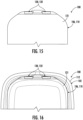
FIG. 15 provides top view of the double-side conductive tape or the double-side conductive foam arranged on the electronic display of the wearable computing device according to another embodiment of the present disclosure; -
FIG. 16 provides top view of the wearable computing device according to another embodiment of the present disclosure, particularly illustrating double-side conductive tape or foam placed on a top surface of the printed circuit board; -
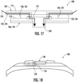
FIG. 17 provides a cross-sectional view of the wearable computing device according to one embodiment of the present disclosure, particularly illustrating first and second biometric sensor electrodes arranged on opposite sides of a printed circuit board and placed on a top surface of the printed circuit board; -
FIG. 18 provides a cross-sectional view of the wearable computing device according to one embodiment of the present disclosure, particularly illustrating first and second biometric sensor electrodes arranged on the same side of a printed circuit board; -
FIG. 19 provides a partial, perspective view of a rear-side of a wearable computing device according to one embodiment of the present disclosure, particularly illustrating first and second biometric sensor electrodes electrically connected to a printed circuit board via single-side conductive tape; -
FIG. 20 provides a partial, perspective view of another rear-side of a wearable computing device according to one embodiment of the present disclosure, particularly illustrating first and second biometric sensor electrodes electrically connected to a printed circuit board via single-side conductive tape; -
FIG. 21 provides a partial, side view of a wearable computing device according to one embodiment of the present disclosure, particularly illustrating first and second biometric sensor electrodes electrically connected to a printed circuit board via single-side conductive tape and conductive adhesive; -
FIG. 22 provides a partial, rear-side view of the wearable computing device ofFIG. 16 , particularly illustrating first and second biometric sensor electrodes electrically connected to a printed circuit board via single-side conductive tape and conductive adhesive; -
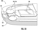
FIG. 23 provides a partial, side view of a wearable computing device according to one embodiment of the present disclosure, particularly illustrating first and second biometric sensor electrodes electrically connected to a printed circuit board via anisotropic conductive film; and -
FIG. 24 provides a flow chart illustrating one embodiment of a method of assembling a wearable computing device according to the present disclosure. - Reference now will be made in detail to embodiments of the invention, one or more examples of which are illustrated in the drawings. The invention is defined by the appended claims.
- For a wearable computing device, the front or top surface is typically occupied by a large electronic display, often covered with an optically clear covering constructed of certain materials (such as glass, polycarbonate, acrylic, etc.). This covering often requires a seal around its perimeter, making the electronic display covering larger than the active region of the electronic display itself. Accordingly, the present disclosure is related to a biometric sensor electrode integrated in the top surface of the covering on a wearable computing device, thereby providing increased surface area and improved signal quality of the sensor. By integrating the biometric sensor electrode onto the covering, the user is able to access the sensor in a more ergonomic manner, allowing the user to make contact with a variety of extremities (palm, fingers, leg, etc.) without requiring high dexterity on a small surface.
- To activate the biometric sensor electrode created on the top surface of the covering, the sensor requires electrically connecting the sensor to the sense hub (which contains the main circuit) in the system board within the wearable computing device. Thus, the present disclosure is also directed to an improved conductive component between the biometric sensor electrode and the main circuit of the wearable computing device. As such, the present disclosure provides for electrically connecting an efficient and effective conductive component to a printed or flexible circuit board through the electronic display module and into the main circuit of the wearable computing device. In particular, the improved conductive component of the present disclosure has a low feed-thru electrical resistance and does not require extra space. Moreover, the integrated biometric sensor electrode allows for an easy assembly process without increasing costs or reducing reliability.
- For example, in an embodiment, a direct/indirect connection may be used with conductive foam and an adhesive (such as anisotropic conductive film (ACF) and silver epoxy). In such an embodiment, physical vapor deposition (PVD) contact pads are positioned on the top surface and sandwiched between the sensor metal bottom of the covering and the top surface of the electronic display module. Next, a low-resistance conductive foam is placed between the sensor metal bottom and the PVD contact pads to connect the biometric sensor electrode to PVD contact pad(s). Further, the PVD contact pad(s) on the top surface is connected to a flexible printed circuit (FBC) through the electronic display module connector. The FBC is bonded on the top surface using an adhesive, such as ACF, by conventional FPC bonding processes. Moreover, the electronic display module connector is secured to the main device body, where the main circuit is located.
- In particular, by providing a conductive component between the biometric sensor electrode and the main circuit of the wearable computing device, it is e.g., possible to obtain a compact and robust design of the wearable computing.
- With reference now to the Figures, example embodiments of the present disclosure will be discussed in further detail.
- Referring now to the drawings,
FIG. 1 illustrates a perspective view of awearable computing device 100 according to the present disclosure. In particular, as shown, thewearable computing device 100 may be worn on a person's forearm like a wristwatch. In addition, as shown, thewearable computing device 100 has ahousing 102 that contains the electronics associated with thewearable computing device 100. Further, as shown, thewearable computing device 100 includes one ormore buttons 104 and anelectronic display 106 that is accessible/visible through thehousing 102. In some embodiments, for example, the button(s) 404 may be implemented to provide a mechanism to activate a heart rate sensor to collect heart rate data. Moreover, in an embodiment, theelectronic display 106 may cover an electronics package 110 (also referred to herein as an electronic display module connector), which is also housed with thehousing 102. In addition, as shown, awristband 108 may be integrated with thehousing 102. - Referring now to
FIGS. 2-7 , various views of thehousing 102 of thewearable computing device 100 according to the present disclosure are illustrated. In particular,FIG. 2 illustrates a top view of one embodiment of thehousing 102 according to the present disclosure;FIG. 3 illustrates a side view of one embodiment of thehousing 102 according to the present disclosure;FIG. 4 illustrates an exploded side view of one embodiment of thehousing 102 according to the present disclosure;FIG. 5 illustrates a transparent, perspective view of one embodiment of thehousing 102 according to the present disclosure;FIG. 6 illustrates a transparent, top view of one embodiment of thehousing 102 according to the present disclosure;FIG. 7 illustrates a transparent, perspective view of one embodiment of thehousing 102 according to the present disclosure; andFIG. 8 illustrates a rear view of one embodiment of theelectronics package 110 within thehousing 102 according to the present disclosure. - Furthermore, as shown generally in
FIGS. 2-7 , thehousing 102 includes anouter covering 112 defining an outer-mosttop surface 114 and anouter perimeter 116. For example, in an embodiment, theouter covering 112 may be constructed of glass, polycarbonate, acrylic, or similar. Thus, as shown particularly inFIG. 7 , aninternal volume 118 is defined, at least in part, by aninner surface 120 of theouter covering 112. In addition, as shown inFIGS. 5 and7 , thewearable computing device 100 may also include aseal 115 arranged along theouter perimeter 116 of theouter covering 112. Thus, in such embodiments, as shown inFIG. 7 , theinternal volume 118 is defined by theinner surface 120 of theouter covering 112 and aninner edge 117 of theseal 115. Accordingly, as shown, theelectronic display 106 and the electronicdisplay module connector 110 may be arranged within theinternal volume 118, as further described herein. - In addition, as shown in
FIGS. 2-7 , thewearable computing device 100 further includes at least one biometric sensor electrode, such as a firstbiometric sensor electrode 122 and a secondbiometric sensor electrode 124, positioned on the outer-mosttop surface 114 of theouter covering 112 and wrapping around one or more side edges of theouter covering 112 to the internal volume 118 (see e.g.,FIG. 7 ). Thus, as shown, in an embodiment, thewearable computing device 100 may include twosensor electrodes sensor electrodes - For example, as shown in
FIG. 7 , in an embodiment, the biometric sensor electrode(s) 122, 124 wrap around the side edge of theouter covering 112 and theinner edge 117 of theseal 115 to theinternal volume 118. Furthermore, in such embodiments, as shown generally inFIGS. 2-7 , the first and secondbiometric sensor electrodes more gaps 126. More specifically, as shown inFIG. 2 , the first and secondbiometric sensor electrodes multiple gaps 126 on opposing sides of theouter covering 112. In other words, as shown, the twosensor electrodes - Moreover, as shown in
FIG. 8 , thewearable computing device 100 includes a printedcircuit board 128 arranged within theinternal volume 118, i.e., on a rear side of theelectronics display 106. Thus, in an embodiment, as shown inFIGS. 8 and12 , the first and secondbiometric sensor electrodes circuit board 128. Alternatively, as shown inFIG. 18 , the first and secondbiometric sensor electrodes circuit board 128. Furthermore, in certain embodiments, the biometric sensor electrode(s) 122, 124 described herein may each include a physical vapor deposition (PVD) sensor pad. In addition, in an embodiment, the biometric sensor electrode(s) 122, 124 described herein may include an electrocardiogram (ECG) sensor, an electrodermal activity (EDA) sensor, or any other suitable sensor type. - Accordingly, the biometric sensor electrode(s) 122, 124 described herein may be connected through inter-media materials to the electronic
display module connector 110, which may include a computing system configured to operate thewearable computing device 100. In particular, as shown inFIG. 9 , a block diagram of anexample computing system 150 according to example embodiments of the present disclosure is illustrated. Further, as shown, in an embodiment, thecomputing system 150 includes auser computing device 152, aserver computing system 160, and atraining computing system 170 that are communicatively coupled over anetwork 180. Thus, in an embodiment, components of theuser computing device 152 may be part of thewearable computing device 100. - In particular, as shown, the
user computing device 152 includes one or more processors 154 and amemory 155. The one or more processors 154 can be any suitable processing device (e.g., a processor core, a microprocessor, an ASIC, an FPGA, a controller, a microcontroller, etc.) and can be one processor or a plurality of processors that are operatively connected. Thememory 155 can include one or more non-transitory computer-readable storage media, such as RAM, ROM, EEPROM, EPROM, flash memory devices, magnetic disks, etc., and combinations thereof. Thememory 155 can storedata 156 andinstructions 157 which are executed by the processor 154 to cause theuser computing device 152 to perform operations. - In some implementations, the
user computing device 152 can store or include one ormore models 158. For example, in an embodiment, the model(s) 158 can be or can otherwise include various machine-learned models such as neural networks (e.g., deep neural networks) or other types of machine-learned models, including non-linear models and/or linear models. Neural networks can include feed-forward neural networks, recurrent neural networks (e.g., long short-term memory recurrent neural networks), convolutional neural networks or other forms of neural networks. - Thus, in some implementations, the model(s) 158 can be received from the
server computing system 160 over thenetwork 180, stored in the usercomputing device memory 155, and then used or otherwise implemented by the processor(s) 154. Additionally, or alternatively, one ormore models 168 can be included in or otherwise stored and implemented by theserver computing system 160 that communicates with theuser computing device 152 according to a client-server relationship. Thus, the model(s) 158 can be stored and implemented at theuser computing device 152 and/or the model(s) 168 can be stored and implemented at theserver computing system 160. - The
user computing device 152 can also include one or moreuser input components 159 that receives user input. For example, theuser input component 159 can be a touch-sensitive component (e.g., a touch-sensitive display screen or a touch pad) that is sensitive to the touch of a user input object (e.g., a finger or a stylus). The touch-sensitive component can serve to implement a virtual keyboard. Other example user input components include a microphone, a traditional keyboard, or other means by which a user can provide user input. - The
server computing system 160 can be any type of computing device, such as, for example, a personal computing device (e.g., laptop or desktop), a mobile computing device (e.g., smartphone or tablet), a gaming console or controller, a wearable computing device, an embedded computing device, or any other type of computing device. Further, as shown, theserver computing system 160 includes one ormore processors 162 and amemory 164. The processor(s) 162 can be any suitable processing device (e.g., a processor core, a microprocessor, an ASIC, an FPGA, a controller, a microcontroller, etc.) and can be one processor or a plurality of processors that are operatively connected. Thememory 164 can include one or more non-transitory computer-readable storage media, such as RAM, ROM, EEPROM, EPROM, flash memory devices, magnetic disks, etc., and combinations thereof. Thememory 164 can storedata 165 andinstructions 166 which are executed by theprocessor 162 to cause theserver computing system 160 to perform operations. - In some implementations, the
server computing system 160 includes or is otherwise implemented by one or more server computing devices. In instances in which theserver computing system 160 includes plural server computing devices, such server computing devices can operate according to sequential computing architectures, parallel computing architectures, or some combination thereof. - As described above, the
server computing system 160 can store or otherwise include one ormore models 168. For example, the model(s) 168 can be or can otherwise include various machine-learned models. Example machine-learned models include neural networks or other multi-layer non-linear models. Example neural networks include feed forward neural networks, deep neural networks, recurrent neural networks, and convolutional neural networks. - The
user computing device 152 and/or theserver computing system 160 can train themodels 158 and/or 168 via interaction with thetraining computing system 170 that is communicatively coupled over thenetwork 180. Thetraining computing system 170 can be separate from theserver computing system 160 or can be a portion of theserver computing system 160. - The
training computing system 170 includes one ormore processors 172 and amemory 174. The processor(s) 172 can be any suitable processing device (e.g., a processor core, a microprocessor, an ASIC, an FPGA, a controller, a microcontroller, etc.) and can be one processor or a plurality of processors that are operatively connected. Thememory 174 can include one or more non-transitory computer-readable storage media, such as RAM, ROM, EEPROM, EPROM, flash memory devices, magnetic disks, etc., and combinations thereof. Thememory 174 can storedata 175 andinstructions 176 which are executed by theprocessor 172 to cause thetraining computing system 170 to perform operations. In some implementations, thetraining computing system 170 includes or is otherwise implemented by one or more server computing devices. Thetraining computing system 170 can also include amodel trainer 177 that trains the machine-learnedmodels 158 and/or 168 stored at theuser computing device 152 and/or theserver computing system 160 using various training or learning techniques. In particular, in an embodiment, themodel trainer 177 can train themodels 158 and/or 168 based on a set oftraining data 178. - The
model trainer 177 includes computer logic utilized to provide desired functionality. Themodel trainer 177 can be implemented in hardware, firmware, and/or software controlling a general purpose processor. For example, in some implementations, themodel trainer 177 includes program files stored on a storage device, loaded into a memory and executed by one or more processors. In other implementations, themodel trainer 177 includes one or more sets of computer-executable instructions that are stored in a tangible computer-readable storage medium such as RAM, hard disk, or optical or magnetic media. - The
network 180 can be any type of communications network, such as a local area network (e.g., intranet), wide area network (e.g., Internet), or some combination thereof and can include any number of wired or wireless links. In general, communication over thenetwork 180 can be carried via any type of wired and/or wireless connection, using a wide variety of communication protocols (e.g., TCP/IP, HTTP, SMTP, FTP), encodings or formats (e.g., HTML, XML), and/or protection schemes (e.g., VPN, secure HTTP, SSL). - Referring now to
FIGS. 10-20 , thewearable computing device 100 of the present disclosure further includes a conductive component 130 electrically connecting the biometric sensor electrode(s) 122, 124 to the printedcircuit board 128 through the electronicdisplay module connector 110. In particular, the conductive component 130 described herein provides a low-resistance path (e.g., on the order of less than about 50 Ohms, in particular less than 10 Ohms). - More specifically, as shown in
FIGS. 10-17 , the conductive component 130 is double-side conductive foam 132 or tape. In one embodiment, for example, and as shown particularly inFIGS. 10, 11 , and14 , the double-side conductive foam 132 or tape may be sandwiched between abottom surface 138 of theouter covering 112 and atop surface 140 of theelectronic display 106. In such embodiments, as shown particularly inFIG. 14 , the signal path, as indicated by arrows 123, travels through theelectronic display 106 first and then through the printedcircuit board 128. Thus, as shown inFIGS. 10, 11 , and14 , in certain embodiments, theelectronic display 106 can be connected through the printedcircuit board 128 by anisotropic conductive film (ACF) bonding. As used herein, ACF bonding generally refers to a lead-free and environmentally friendly adhesive interconnect film system or paste that can be used to make electrical and mechanical connections. Further, as shown, conductive line(s) 142 connected to the biometric sensor electrode(s) 122, 124 and the conductive component 130 are connected to the printedcircuit board 128 to deliver the sensing signal to theelectronics package 110. - In alternative embodiments, as shown in
FIGS. 15-17 , the double-side conductive foam 132 or tape may be placed on atop surface 121 of the printedcircuit board 128. In such embodiments, as shown, theelectronic display 106 becomes part of the printed circuit board 128 (i.e., its top surface). Accordingly, as shown particularly inFIG. 17 , the double-side conductive foam 132 or tape is configured to sit on thetop surface 121 of the printed circuit board 128 (e.g., on the wing side top surface of the electronic display 106). In such embodiments, as shown particularly inFIG. 17 , the signal path, as indicated byarrows 125, travels by theelectronic display 106 and directly through the printedcircuit board 128. - Alternatively, as shown in
FIGS. 19-20 , the conductive component 130 is double-side conductive tape 134 or film. In such embodiments, as shown, the conductive tape 134 or film may be applied directly to the biometric sensor electrode(s) 122, 124 to electrically connect the biometric sensor electrode(s) 122, 124 to the printedcircuit board 128. More particularly, as shown, the biometric sensor electrode(s) 122, 124 wrap around the side edge of theouter covering 112 to theinternal volume 118 such that a first end of the conductive tape 134 or film can be secured to an end of the biometric sensor electrode(s) 122, 124 and an opposing end of the conductive tape 134 or film can be secured directly to the printed circuit board 128 (or to a conductive component in direct contact with the printed circuit board 128). Furthermore, in such embodiments, the conductive component 130 may include separate conductive tapes or a single conductive tape with two conductive lines. - Referring now to
FIG. 21 , the conductive component 130 is ACF (anisotropic conductive film or paste) bonding 135. In such embodiments, as an example, the ACF bonding 135 can be applied directly to the biometric sensor electrode(s) 122, 124 to electrically connect the biometric sensor electrode(s) 122, 124 to the printedcircuit board 128. In such embodiments, the ACF bonding 135 can be used alone or in combination with the conductive tape 134 or film to provide additional support. Thus, in such embodiments, as shown at step (1), the ACF bonding 135 can be connected to the biometric sensor electrode(s) 122, 124, which are located on a hard glass surface. As shown at step (2), the electronics display 106 can then be laminated on top of the ACF bonding 135. Moreover, as shown at step (3), the ACF bonding 135 can be connected to the printedcircuit board 128 or any suitable location that can ultimately be electrically connected to the printedcircuit board 128. Such a connection can be completed using, for example, soldering, connectors, springs, fasteners, or similar. - In still another embodiment, as shown in
FIGS. 22-23 , the conductive component 130 is a conductive adhesive 136 through direct contact, such as, for example, silver epoxy. In still further embodiments, the conductive component 130 may be single-side conductive tape, single-side conductive foam, anisotropic conductive film, or combinations thereof. In further embodiments, any suitable connection is possible to connect such components together to define the desired low-resistance path. - In still further embodiments, as shown in
FIGS. 10 and 11 , thewearable computing device 100 may further include acontact pad 144 arranged between the double-side conductive foam 130, 132 or tape and thetop surface 140 of theelectronic display 106. In such embodiments, for example, thecontact pad 144 may be a thin metal film. Thus, as shown, the printedcircuit board 128 is electrically coupled to an edge of thecontact pad 144, e.g., through conductive line(s) 142. In further embodiments, the printedcircuit board 128 may be arranged adjacent to thecontact pad 144 and may be electrically connected to a bottom surface of thecontact pad 144 such that the conductive line(s) 142 can be omitted. - Referring now to
FIG. 24 , a flow diagram of one embodiment of amethod 200 of assembling a wearable computing device is provided. In an embodiment, for example, the wearable computing device may be any suitable wearable computing device such as thewearable computing device 100 described herein with reference toFIGS. 1-23 . In general, themethod 200 is described herein with reference to thewearable computing device 100 ofFIGS. 1-24 . However, it should be appreciated that the disclosedmethod 200 may be implemented with any other suitable wearable computing device having any other suitable configurations. In addition, althoughFIG. 24 depicts steps performed in a particular order for purposes of illustration and discussion, the methods discussed herein are not limited to any particular order or arrangement. One skilled in the art, using the disclosures provided herein, will appreciate that various steps of the methods disclosed herein can be omitted, rearranged, combined, and/or adapted in various ways without deviating from the scope of the present disclosure. - As shown at (202), the
method 200 includes providing an outer covering defining an outer-most top surface and an outer perimeter, an inner surface of the outer covering defining an internal volume. For example,FIGS. 2-7 generally illustrate an embodiment of theouter covering 112 according to the present disclosure. Referring back toFIG. 24 , as shown at (204), themethod 200 includes positioning a first portion of at least one biometric sensor electrode on the outer-most top surface of the outer covering and wrapping a second portion of the at least one biometric sensor electrode around one or more side edges of the outer covering such that the second portion is within the internal volume. For example,FIGS. 2-7 generally illustrate an embodiment of a first portion of thebiometric sensor electrodes top surface 114 of theouter covering 112. Furthermore, as shown particularly inFIGS. 5 ,7 ,15, 16 ,18 , and19 , a second portion of thebiometric sensor electrodes outer covering 112 such that the second portion is within theinternal volume 118 of thewearable computing device 100 according to the present disclosure. - Referring back to
FIG. 24 , as shown at (206), themethod 200 includes placing an electronic display and an electronic display module connector within the internal volume. As shown at (208), themethod 200 includes arranging a printed circuit board within the internal volume adjacent to the electronic display. - As shown at (210), the
method 200 includes electrically connecting the biometric sensor electrode(s) to the printed circuit board through the electronic display module connector via at least one conductive component. In such embodiments, the conductive component(s) defines a low-resistance path. For example, in an embodiment, as shown inFIGS. 10-14 , electrically connecting the biometric sensor electrode(s) 122, 124 to the printedcircuit board 128 through the electronicdisplay module connector 110 includes placing the conductive component(s) 130 between thebottom surface 138 of theouter covering 112 and a top surface of 119 theelectronic display 106. In alternative embodiments, as shown inFIG. 15-17 , electrically connecting the biometric sensor electrode(s) 122, 124 to the printedcircuit board 128 through the electronicdisplay module connector 110 includes placing the conductive component(s) 130 on atop surface 121 of the printedcircuit board 128. In addition, in certain embodiments, as described herein, the conductive component(s) 130 may be double-side conductive tape, double-side conductive foam, single-side conductive tape, single-side conductive foam, conductive adhesive, anisotropic conductive film, or combinations thereof. In an embodiment, for example, wherein the conductive component 130 is the double-side conductive tape or the double-side conductive foam, themethod 200 may include laminating theouter covering 112, the double-side conductive tape or the double-side conductive foam 132, and the biometric sensor electrode(s) 122, 124 together. - The technology discussed herein makes reference to servers, databases, software applications, and other computer-based systems, as well as actions taken and information sent to and from such systems. The inherent flexibility of computer-based systems allows for a great variety of possible configurations, combinations, and divisions of tasks and functionality between and among components. For instance, processes discussed herein can be implemented using a single device or component or multiple devices or components working in combination. Databases and applications can be implemented on a single system or distributed across multiple systems. Distributed components can operate sequentially or in parallel.
- The invention is defined by the appended claims.
Claims (14)
- A wearable computing device (100), comprising:an outer covering (112) defining an outer-most top surface (114) and an outer perimeter (116);an internal volume (118) defined, at least in part, by an inner surface (120) of the outer covering (112);
an electronic display (106) and an electronic display module connector arranged within the internal volume (118);at least one biometric sensor electrode (122, 124) positioned on the outer-most top surface (114) of the
outer covering (112) and wrapping around one or more side edges of the outer covering (112) to the internal volume (118);a printed circuit board (128) arranged within the internal volume (118); anda conductive component (130) electrically connecting the at least one biometric sensor electrode to the printed circuit board (128) through the electronic display module connector. - The wearable computing device of claim 1, further comprising a seal (115) arranged along the outer perimeter (116) of the outer covering (112), the internal volume (118) being defined by the inner surface (120) of the outer covering (112) and an inner edge (117) of the seal (115), the at least one biometric sensor electrode (122, 124) wrapping around the one or more side edges of the outer covering (112) and the inner edge (117) of the seal (115) to the internal volume (118).
- The wearable computing device of claims 1 or 2, wherein the conductive component (130) comprises at least one of double-side conductive tape, double-side conductive foam, single-side conductive tape, single-side conductive foam, conductive adhesive, anisotropic conductive film, or combinations thereof.
- The wearable computing device of claim 3, wherein the conductive component (130) between the at least one biometric sensor electrode (122, 124) and the printed circuit board (128) comprises the double-side conductive tape or the double-side conductive foam, the double-side conductive tape or the double-side conductive foam being sandwiched between a bottom surface of the outer covering (112) and a top surface of the electronic display (106).
- The wearable computing device of claims 3 or 4, further comprising a contact pad arranged between the double-side conductive tape or the double-side conductive foam and the top surface of the electronic display.
- The wearable computing device of claim 5, wherein the contact pad comprises a thin metal film or wherein the printed circuit board is electrically coupled to an edge of the contact pad or wherein the printed circuit board (128) is arranged adjacent to the contact pad and is electrically connected to a bottom surface of the contact pad.
- The wearable computing device of claim 3, wherein the conductive component between the at least one biometric sensor electrode (122, 124) and the printed circuit board (128) comprises the double-side conductive tape or the double-side conductive foam, the double-side conductive tape or the double-side conductive foam being on a top surface of the printed circuit board (128).
- The wearable computing device of any of the preceding claims, wherein the at least one biometric sensor electrode (122, 124) comprises, at least, a first biometric sensor electrode (122) and a second biometric sensor electrode (124), the first and second biometric sensor electrodes (122, 124) being spaced apart by a gap.
- The wearable computing device of claim 8, wherein the first and second biometric sensor electrodes (122, 124) are arranged on the same side of the printed circuit board (128) or wherein the first and second biometric sensor electrodes (122, 124) are arranged on opposite sides of the printed circuit board (128)
- The wearable computing device of any of the preceding claims, wherein the at least one biometric sensor electrode (122, 124) comprises a physical vapor deposition (PVD) sensorpad and / or wherein the outer covering (112) is constructed of at least one of glass, poly carbonate, or acrylic.
- The wearable computing device of any of the preceding claims, wherein the at least one biometric sensor electrode (122, 124) comprises at least one of an electrocardiogram (ECG)sensor or an electrodermal activity (EDA) sensor.
- A method of assembling a wearable computing device, the method comprising:providing an outer covering (112) defining an outer-most top surface (114) and an outer perimeter (116), an inner surface (120) of the outer covering (112) defining an internal volume (118);positioning a first portion of at least one biometric sensor electrode (122, 124) on the outer-most top surface (114) of the outer covering (112) and wrapping a second portion of the at least one biometric sensor electrode (122, 124) around one or more side edges of the outer covering (112)such that the second portion is within the internal volume (118);placing an electronic display (106) and an electronic display module connector within the internal volume (118);arranging a printed circuit board (128) within the internal volume (118) adjacent to the electronic display (106); and electrically connecting the at least one biometric sensor electrode (122, 124) to the printed circuit board (128) through the electronic display module connector via at least one conductive component (130).
- The method of claim 12, wherein electrically connecting the at least one biometric sensor electrode (122, 124) to the electronic display module connector through the printed circuit board (128) further comprises placing the at least one conductive component (130) between a bottom surface of the outer covering (112) and a top surface of the electronic display (106) or on a top surface of the printed circuit board (128), the at least one conductive component (130) comprising at least one of double-side conductive tape, double-side conductive foam, single-side conductive tape, single-side conductive foam, conductive adhesive, anisotropic conductive film, or combinations thereof.
- The method of claim 13, wherein the conductive component (130) between the at least one biometric sensor electrode (122, 124) and the printed circuit board (128) comprises the double-side conductive tape or the double-side conductive foam, the method further comprising laminating the outer covering (112), the double-side conductive tape or the double-side conductive foam, and the at least one biometric sensor electrode (122, 124) together, in particular further comprising placing a contact pad adjacent the double-side conductive tape or the double-side conductive foam, more in particular comprising electrically connecting the printed circuit board (128) to an edge of the contact pad.
Applications Claiming Priority (1)
| Application Number | Priority Date | Filing Date | Title |
|---|---|---|---|
| PCT/US2021/042169 WO2023003529A1 (en) | 2021-07-19 | 2021-07-19 | Biometric sensor integrated with electronic display of a wearable device |
Publications (2)
| Publication Number | Publication Date |
|---|---|
| EP4157091A1 EP4157091A1 (en) | 2023-04-05 |
| EP4157091B1 true EP4157091B1 (en) | 2025-04-02 |
Family
ID=77398635
Family Applications (1)
| Application Number | Title | Priority Date | Filing Date |
|---|---|---|---|
| EP21756095.2A Active EP4157091B1 (en) | 2021-07-19 | 2021-07-19 | Biometric sensor integrated with electronic display of a wearable device |
Country Status (6)
| Country | Link |
|---|---|
| US (1) | US20230255559A1 (en) |
| EP (1) | EP4157091B1 (en) |
| JP (1) | JP7555437B2 (en) |
| KR (1) | KR20230031844A (en) |
| CN (1) | CN116075271A (en) |
| WO (1) | WO2023003529A1 (en) |
Families Citing this family (2)
| Publication number | Priority date | Publication date | Assignee | Title |
|---|---|---|---|---|
| US20250219669A1 (en) * | 2023-12-29 | 2025-07-03 | Google Llc | Computing Device Having Sensor with Integrated Antenna |
| CN119964458B (en) * | 2025-01-16 | 2025-11-14 | 昆山国显光电有限公司 | Display panel, display module and display device |
Family Cites Families (15)
| Publication number | Priority date | Publication date | Assignee | Title |
|---|---|---|---|---|
| US10042422B2 (en) * | 2013-11-12 | 2018-08-07 | Thalmic Labs Inc. | Systems, articles, and methods for capacitive electromyography sensors |
| WO2015126095A1 (en) * | 2014-02-21 | 2015-08-27 | 삼성전자 주식회사 | Electronic device |
| TWM493362U (en) * | 2014-08-26 | 2015-01-11 | 華碩電腦股份有限公司 | Wearable electronic device |
| US10599101B2 (en) * | 2014-09-02 | 2020-03-24 | Apple Inc. | Wearable electronic device |
| KR20170118439A (en) * | 2016-04-15 | 2017-10-25 | 삼성전자주식회사 | Electronic device for measuring biometric data and device for charging the electronic device |
| US9870033B1 (en) | 2016-08-30 | 2018-01-16 | Apple Inc. | Sensor assemblies for electronic devices |
| KR102567892B1 (en) | 2016-09-05 | 2023-08-17 | 삼성전자주식회사 | Electronic Device Involving Multi-Band Antenna |
| US10729347B1 (en) | 2017-01-31 | 2020-08-04 | Verily Life Sciences Llc | Device with light-processing component covered by light-permeable touchable electrode for detecting biologic activity |
| KR102739761B1 (en) * | 2017-02-03 | 2024-12-09 | 삼성전자주식회사 | Electronic device with body information detection function |
| KR102717009B1 (en) * | 2017-02-21 | 2024-10-15 | 삼성전자주식회사 | Electronic device for measuring biometric information |
| US11122688B2 (en) * | 2017-05-05 | 2021-09-14 | Bloomer Health Tech., Inc. | Padded, flexible encasing for body monitoring systems in fabrics |
| US10957969B2 (en) * | 2017-09-11 | 2021-03-23 | Apple Inc. | Integrated antennas for portable electronic devices |
| JP6949638B2 (en) * | 2017-09-15 | 2021-10-13 | オムロンヘルスケア株式会社 | Pulse wave measurement unit and pulse wave measurement device |
| EP3626159A1 (en) * | 2018-09-24 | 2020-03-25 | Koninklijke Philips N.V. | Body mountable sensor unit |
| KR102848437B1 (en) * | 2019-07-31 | 2025-08-21 | 삼성전자주식회사 | Electronic device having electrode measuring biological signal |
-
2021
- 2021-07-19 JP JP2022580522A patent/JP7555437B2/en active Active
- 2021-07-19 WO PCT/US2021/042169 patent/WO2023003529A1/en not_active Ceased
- 2021-07-19 EP EP21756095.2A patent/EP4157091B1/en active Active
- 2021-07-19 CN CN202180046338.9A patent/CN116075271A/en active Pending
- 2021-07-19 US US18/013,717 patent/US20230255559A1/en active Pending
- 2021-07-19 KR KR1020227045944A patent/KR20230031844A/en not_active Ceased
Also Published As
| Publication number | Publication date |
|---|---|
| WO2023003529A1 (en) | 2023-01-26 |
| JP2024508200A (en) | 2024-02-26 |
| EP4157091A1 (en) | 2023-04-05 |
| US20230255559A1 (en) | 2023-08-17 |
| CN116075271A (en) | 2023-05-05 |
| KR20230031844A (en) | 2023-03-07 |
| JP7555437B2 (en) | 2024-09-24 |
Similar Documents
| Publication | Publication Date | Title |
|---|---|---|
| CN205050119U (en) | A touch input device for detecting electrode slice of pressure reaches including this electrode slice | |
| CN102368949B (en) | ECG signal detection device | |
| JP3871991B2 (en) | Touch panel | |
| US20230255559A1 (en) | Biometric Sensor Integrated with Electronic Display of a Wearable Device | |
| JP6527343B2 (en) | Touch input device | |
| CN205068342U (en) | Touch input device | |
| EP3977240B1 (en) | Motion-restricting apparatus with common base electrode | |
| TWI490742B (en) | Touch panel | |
| US20130259329A1 (en) | Fingerprint sensor packagings and methods | |
| US10114411B2 (en) | Electronic device and manufacturing method therefor | |
| JP6146998B2 (en) | Electronics | |
| CN106872583B (en) | Ultrasonic sensor | |
| JP2019502203A (en) | Electrode sheet capable of detecting pressure applied with temperature compensation and touch input device | |
| KR101693337B1 (en) | Touch input device | |
| CN104067298A (en) | Information gathering device | |
| KR101838570B1 (en) | Electrode sheet and touch input device | |
| JP6965955B2 (en) | Information gathering device | |
| KR101865304B1 (en) | Touch input device | |
| TW200839361A (en) | Anti-EMI touch panel and liquid crystal display using same | |
| TW201913347A (en) | Wearable electronic device and reflective capacitive touch panel thereof | |
| KR20260027021A (en) | Electronic device, method, and non-transitory computer readable storage medium for recording food intake pattern | |
| CN103279227A (en) | Touch detection device | |
| WO2025209318A1 (en) | Button module and electronic device | |
| KR20170067134A (en) | Electrode sheet and touch input device for detecting pressure with temperature compensation | |
| CN103271730A (en) | Touch detection device |
Legal Events
| Date | Code | Title | Description |
|---|---|---|---|
| STAA | Information on the status of an ep patent application or granted ep patent |
Free format text: STATUS: UNKNOWN |
|
| STAA | Information on the status of an ep patent application or granted ep patent |
Free format text: STATUS: THE INTERNATIONAL PUBLICATION HAS BEEN MADE |
|
| PUAI | Public reference made under article 153(3) epc to a published international application that has entered the european phase |
Free format text: ORIGINAL CODE: 0009012 |
|
| STAA | Information on the status of an ep patent application or granted ep patent |
Free format text: STATUS: REQUEST FOR EXAMINATION WAS MADE |
|
| 17P | Request for examination filed |
Effective date: 20221229 |
|
| AK | Designated contracting states |
Kind code of ref document: A1 Designated state(s): AL AT BE BG CH CY CZ DE DK EE ES FI FR GB GR HR HU IE IS IT LI LT LU LV MC MK MT NL NO PL PT RO RS SE SI SK SM TR |
|
| DAV | Request for validation of the european patent (deleted) | ||
| DAX | Request for extension of the european patent (deleted) | ||
| GRAP | Despatch of communication of intention to grant a patent |
Free format text: ORIGINAL CODE: EPIDOSNIGR1 |
|
| STAA | Information on the status of an ep patent application or granted ep patent |
Free format text: STATUS: GRANT OF PATENT IS INTENDED |
|
| INTG | Intention to grant announced |
Effective date: 20241218 |
|
| GRAS | Grant fee paid |
Free format text: ORIGINAL CODE: EPIDOSNIGR3 |
|
| GRAA | (expected) grant |
Free format text: ORIGINAL CODE: 0009210 |
|
| STAA | Information on the status of an ep patent application or granted ep patent |
Free format text: STATUS: THE PATENT HAS BEEN GRANTED |
|
| AK | Designated contracting states |
Kind code of ref document: B1 Designated state(s): AL AT BE BG CH CY CZ DE DK EE ES FI FR GB GR HR HU IE IS IT LI LT LU LV MC MK MT NL NO PL PT RO RS SE SI SK SM TR |
|
| P01 | Opt-out of the competence of the unified patent court (upc) registered |
Free format text: CASE NUMBER: APP_9176/2025 Effective date: 20250224 |
|
| REG | Reference to a national code |
Ref country code: GB Ref legal event code: FG4D |
|
| REG | Reference to a national code |
Ref country code: CH Ref legal event code: EP |
|
| REG | Reference to a national code |
Ref country code: IE Ref legal event code: FG4D |
|
| REG | Reference to a national code |
Ref country code: DE Ref legal event code: R096 Ref document number: 602021028576 Country of ref document: DE |
|
| REG | Reference to a national code |
Ref country code: NL Ref legal event code: MP Effective date: 20250402 |
|
| PG25 | Lapsed in a contracting state [announced via postgrant information from national office to epo] |
Ref country code: NL Free format text: LAPSE BECAUSE OF FAILURE TO SUBMIT A TRANSLATION OF THE DESCRIPTION OR TO PAY THE FEE WITHIN THE PRESCRIBED TIME-LIMIT Effective date: 20250402 |
|
| REG | Reference to a national code |
Ref country code: AT Ref legal event code: MK05 Ref document number: 1780472 Country of ref document: AT Kind code of ref document: T Effective date: 20250402 |
|
| PG25 | Lapsed in a contracting state [announced via postgrant information from national office to epo] |
Ref country code: FI Free format text: LAPSE BECAUSE OF FAILURE TO SUBMIT A TRANSLATION OF THE DESCRIPTION OR TO PAY THE FEE WITHIN THE PRESCRIBED TIME-LIMIT Effective date: 20250402 Ref country code: ES Free format text: LAPSE BECAUSE OF FAILURE TO SUBMIT A TRANSLATION OF THE DESCRIPTION OR TO PAY THE FEE WITHIN THE PRESCRIBED TIME-LIMIT Effective date: 20250402 Ref country code: PT Free format text: LAPSE BECAUSE OF FAILURE TO SUBMIT A TRANSLATION OF THE DESCRIPTION OR TO PAY THE FEE WITHIN THE PRESCRIBED TIME-LIMIT Effective date: 20250804 |
|
| PGFP | Annual fee paid to national office [announced via postgrant information from national office to epo] |
Ref country code: DE Payment date: 20250729 Year of fee payment: 5 |
|
| REG | Reference to a national code |
Ref country code: LT Ref legal event code: MG9D |
|
| PG25 | Lapsed in a contracting state [announced via postgrant information from national office to epo] |
Ref country code: NO Free format text: LAPSE BECAUSE OF FAILURE TO SUBMIT A TRANSLATION OF THE DESCRIPTION OR TO PAY THE FEE WITHIN THE PRESCRIBED TIME-LIMIT Effective date: 20250702 Ref country code: GR Free format text: LAPSE BECAUSE OF FAILURE TO SUBMIT A TRANSLATION OF THE DESCRIPTION OR TO PAY THE FEE WITHIN THE PRESCRIBED TIME-LIMIT Effective date: 20250703 |
|
| PG25 | Lapsed in a contracting state [announced via postgrant information from national office to epo] |
Ref country code: PL Free format text: LAPSE BECAUSE OF FAILURE TO SUBMIT A TRANSLATION OF THE DESCRIPTION OR TO PAY THE FEE WITHIN THE PRESCRIBED TIME-LIMIT Effective date: 20250402 |
|
| PG25 | Lapsed in a contracting state [announced via postgrant information from national office to epo] |
Ref country code: BG Free format text: LAPSE BECAUSE OF FAILURE TO SUBMIT A TRANSLATION OF THE DESCRIPTION OR TO PAY THE FEE WITHIN THE PRESCRIBED TIME-LIMIT Effective date: 20250402 |
|
| PGFP | Annual fee paid to national office [announced via postgrant information from national office to epo] |
Ref country code: GB Payment date: 20250728 Year of fee payment: 5 |
|
| PG25 | Lapsed in a contracting state [announced via postgrant information from national office to epo] |
Ref country code: HR Free format text: LAPSE BECAUSE OF FAILURE TO SUBMIT A TRANSLATION OF THE DESCRIPTION OR TO PAY THE FEE WITHIN THE PRESCRIBED TIME-LIMIT Effective date: 20250402 |
|
| PG25 | Lapsed in a contracting state [announced via postgrant information from national office to epo] |
Ref country code: AT Free format text: LAPSE BECAUSE OF FAILURE TO SUBMIT A TRANSLATION OF THE DESCRIPTION OR TO PAY THE FEE WITHIN THE PRESCRIBED TIME-LIMIT Effective date: 20250402 |
|
| PG25 | Lapsed in a contracting state [announced via postgrant information from national office to epo] |
Ref country code: RS Free format text: LAPSE BECAUSE OF FAILURE TO SUBMIT A TRANSLATION OF THE DESCRIPTION OR TO PAY THE FEE WITHIN THE PRESCRIBED TIME-LIMIT Effective date: 20250702 |
|
| PG25 | Lapsed in a contracting state [announced via postgrant information from national office to epo] |
Ref country code: IS Free format text: LAPSE BECAUSE OF FAILURE TO SUBMIT A TRANSLATION OF THE DESCRIPTION OR TO PAY THE FEE WITHIN THE PRESCRIBED TIME-LIMIT Effective date: 20250802 |
|
| PG25 | Lapsed in a contracting state [announced via postgrant information from national office to epo] |
Ref country code: LV Free format text: LAPSE BECAUSE OF FAILURE TO SUBMIT A TRANSLATION OF THE DESCRIPTION OR TO PAY THE FEE WITHIN THE PRESCRIBED TIME-LIMIT Effective date: 20250402 |
|
| REG | Reference to a national code |
Ref country code: DE Ref legal event code: R097 Ref document number: 602021028576 Country of ref document: DE |
|
| PG25 | Lapsed in a contracting state [announced via postgrant information from national office to epo] |
Ref country code: DK Free format text: LAPSE BECAUSE OF FAILURE TO SUBMIT A TRANSLATION OF THE DESCRIPTION OR TO PAY THE FEE WITHIN THE PRESCRIBED TIME-LIMIT Effective date: 20250402 Ref country code: SM Free format text: LAPSE BECAUSE OF FAILURE TO SUBMIT A TRANSLATION OF THE DESCRIPTION OR TO PAY THE FEE WITHIN THE PRESCRIBED TIME-LIMIT Effective date: 20250402 |
|
| PG25 | Lapsed in a contracting state [announced via postgrant information from national office to epo] |
Ref country code: CZ Free format text: LAPSE BECAUSE OF FAILURE TO SUBMIT A TRANSLATION OF THE DESCRIPTION OR TO PAY THE FEE WITHIN THE PRESCRIBED TIME-LIMIT Effective date: 20250402 |
|
| PG25 | Lapsed in a contracting state [announced via postgrant information from national office to epo] |
Ref country code: EE Free format text: LAPSE BECAUSE OF FAILURE TO SUBMIT A TRANSLATION OF THE DESCRIPTION OR TO PAY THE FEE WITHIN THE PRESCRIBED TIME-LIMIT Effective date: 20250402 |
|
| PG25 | Lapsed in a contracting state [announced via postgrant information from national office to epo] |
Ref country code: SK Free format text: LAPSE BECAUSE OF FAILURE TO SUBMIT A TRANSLATION OF THE DESCRIPTION OR TO PAY THE FEE WITHIN THE PRESCRIBED TIME-LIMIT Effective date: 20250402 |
|
| PG25 | Lapsed in a contracting state [announced via postgrant information from national office to epo] |
Ref country code: IT Free format text: LAPSE BECAUSE OF FAILURE TO SUBMIT A TRANSLATION OF THE DESCRIPTION OR TO PAY THE FEE WITHIN THE PRESCRIBED TIME-LIMIT Effective date: 20250402 |
|
| PLBE | No opposition filed within time limit |
Free format text: ORIGINAL CODE: 0009261 |
|
| STAA | Information on the status of an ep patent application or granted ep patent |
Free format text: STATUS: NO OPPOSITION FILED WITHIN TIME LIMIT |
|
| PG25 | Lapsed in a contracting state [announced via postgrant information from national office to epo] |
Ref country code: RO Free format text: LAPSE BECAUSE OF FAILURE TO SUBMIT A TRANSLATION OF THE DESCRIPTION OR TO PAY THE FEE WITHIN THE PRESCRIBED TIME-LIMIT Effective date: 20250402 |
|
| REG | Reference to a national code |
Ref country code: CH Ref legal event code: L10 Free format text: ST27 STATUS EVENT CODE: U-0-0-L10-L00 (AS PROVIDED BY THE NATIONAL OFFICE) Effective date: 20260211 |
|
| REG | Reference to a national code |
Ref country code: CH Ref legal event code: H13 Free format text: ST27 STATUS EVENT CODE: U-0-0-H10-H13 (AS PROVIDED BY THE NATIONAL OFFICE) Effective date: 20260224 |
|
| 26N | No opposition filed |
Effective date: 20260105 |
|
| PG25 | Lapsed in a contracting state [announced via postgrant information from national office to epo] |
Ref country code: LU Free format text: LAPSE BECAUSE OF NON-PAYMENT OF DUE FEES Effective date: 20250719 |
|
| REG | Reference to a national code |
Ref country code: BE Ref legal event code: MM Effective date: 20250731 |
|
| PG25 | Lapsed in a contracting state [announced via postgrant information from national office to epo] |
Ref country code: BE Free format text: LAPSE BECAUSE OF NON-PAYMENT OF DUE FEES Effective date: 20250731 |
|
| PG25 | Lapsed in a contracting state [announced via postgrant information from national office to epo] |
Ref country code: FR Free format text: LAPSE BECAUSE OF NON-PAYMENT OF DUE FEES Effective date: 20250731 |
|
| PG25 | Lapsed in a contracting state [announced via postgrant information from national office to epo] |
Ref country code: CH Free format text: LAPSE BECAUSE OF NON-PAYMENT OF DUE FEES Effective date: 20250731 |