EP4156508A1 - Doherty amplifier - Google Patents
Doherty amplifier Download PDFInfo
- Publication number
- EP4156508A1 EP4156508A1 EP20941985.2A EP20941985A EP4156508A1 EP 4156508 A1 EP4156508 A1 EP 4156508A1 EP 20941985 A EP20941985 A EP 20941985A EP 4156508 A1 EP4156508 A1 EP 4156508A1
- Authority
- EP
- European Patent Office
- Prior art keywords
- amplification element
- signal
- auxiliary
- auxiliary amplification
- phase
- Prior art date
- Legal status (The legal status is an assumption and is not a legal conclusion. Google has not performed a legal analysis and makes no representation as to the accuracy of the status listed.)
- Granted
Links
Images


Classifications
-
- H—ELECTRICITY
- H03—ELECTRONIC CIRCUITRY
- H03F—AMPLIFIERS
- H03F1/00—Details of amplifiers with only discharge tubes, only semiconductor devices or only unspecified devices as amplifying elements
- H03F1/02—Modifications of amplifiers to raise the efficiency, e.g. gliding Class A stages, use of an auxiliary oscillation
- H03F1/0205—Modifications of amplifiers to raise the efficiency, e.g. gliding Class A stages, use of an auxiliary oscillation in transistor amplifiers
- H03F1/0288—Modifications of amplifiers to raise the efficiency, e.g. gliding Class A stages, use of an auxiliary oscillation in transistor amplifiers using a main and one or several auxiliary peaking amplifiers whereby the load is connected to the main amplifier using an impedance inverter, e.g. Doherty amplifiers
-
- H—ELECTRICITY
- H03—ELECTRONIC CIRCUITRY
- H03F—AMPLIFIERS
- H03F1/00—Details of amplifiers with only discharge tubes, only semiconductor devices or only unspecified devices as amplifying elements
- H03F1/42—Modifications of amplifiers to extend the bandwidth
-
- H—ELECTRICITY
- H03—ELECTRONIC CIRCUITRY
- H03F—AMPLIFIERS
- H03F1/00—Details of amplifiers with only discharge tubes, only semiconductor devices or only unspecified devices as amplifying elements
- H03F1/56—Modifications of input or output impedances, not otherwise provided for
- H03F1/565—Modifications of input or output impedances, not otherwise provided for using inductive elements
-
- H—ELECTRICITY
- H03—ELECTRONIC CIRCUITRY
- H03F—AMPLIFIERS
- H03F3/00—Amplifiers with only discharge tubes or only semiconductor devices as amplifying elements
- H03F3/60—Amplifiers in which coupling networks have distributed constants, e.g. with waveguide resonators
- H03F3/602—Combinations of several amplifiers
-
- H—ELECTRICITY
- H03—ELECTRONIC CIRCUITRY
- H03F—AMPLIFIERS
- H03F3/00—Amplifiers with only discharge tubes or only semiconductor devices as amplifying elements
- H03F3/68—Combinations of amplifiers, e.g. multi-channel amplifiers for stereophonics
-
- H—ELECTRICITY
- H03—ELECTRONIC CIRCUITRY
- H03H—IMPEDANCE NETWORKS, e.g. RESONANT CIRCUITS; RESONATORS
- H03H7/00—Multiple-port networks comprising only passive electrical elements as network components
- H03H7/01—Frequency selective two-port networks
- H03H7/06—Frequency selective two-port networks including resistors
- H03H7/07—Bridged T-filters
-
- H—ELECTRICITY
- H03—ELECTRONIC CIRCUITRY
- H03F—AMPLIFIERS
- H03F2200/00—Indexing scheme relating to amplifiers
- H03F2200/267—A capacitor based passive circuit, e.g. filter, being used in an amplifying circuit
-
- H—ELECTRICITY
- H03—ELECTRONIC CIRCUITRY
- H03F—AMPLIFIERS
- H03F2200/00—Indexing scheme relating to amplifiers
- H03F2200/318—A matching circuit being used as coupling element between two amplifying stages
-
- H—ELECTRICITY
- H03—ELECTRONIC CIRCUITRY
- H03F—AMPLIFIERS
- H03F2200/00—Indexing scheme relating to amplifiers
- H03F2200/408—Indexing scheme relating to amplifiers the output amplifying stage of an amplifier comprising three power stages
-
- H—ELECTRICITY
- H03—ELECTRONIC CIRCUITRY
- H03F—AMPLIFIERS
- H03F2200/00—Indexing scheme relating to amplifiers
- H03F2200/411—Indexing scheme relating to amplifiers the output amplifying stage of an amplifier comprising two power stages
-
- H—ELECTRICITY
- H03—ELECTRONIC CIRCUITRY
- H03F—AMPLIFIERS
- H03F2200/00—Indexing scheme relating to amplifiers
- H03F2200/451—Indexing scheme relating to amplifiers the amplifier being a radio frequency amplifier
Definitions
- the present disclosure relates to a Doherty amplifier.
- Doherty amplifiers used as amplifiers for wireless communications there are Doherty amplifiers in each of which two carrier amplifiers are connected in series and two peak amplifiers are connected in series.
- a loop in which one of two signals into which a signal is split by the splitter circuit passes through each of the following circuits: the carrier amplifier, the combiner and the peak amplifier, and then returns to the splitter circuit may be formed.
- a splitter circuit includes a low pass filter which is a ⁇ type circuit and a high pass filter which is a T type circuit (for example, refer to Patent Literature 1).
- Patent Literature 1 WO 2017/119062
- a Doherty amplifier including: a first main amplification element to amplify a first signal; a second main amplification element to amplify the first signal amplified by the first main amplification element; a first auxiliary amplification element to amplify a second signal; a second auxiliary amplification element to amplify the second signal amplified by the first auxiliary amplification element; a combination circuit to combine the first signal amplified by the second main amplification element and the second signal amplified by the second auxiliary amplification element; and a phase adjustment circuit connected between the first auxiliary amplification element and the second auxiliary amplification element, in which the phase adjustment circuit adjusts either a phase of a return signal going to the first auxiliary amplification element as a result of passage of the first signal amplified by the second main amplification element through the second auxiliary amplification element as the return signal, or a phase of the return signal going to the second auxiliary amplification
- an oscillation phenomenon occurring between the first auxiliary amplification element and the second auxiliary amplification element can be prevented.
- Fig. 1 is a schematic diagram showing a Doherty amplifier according to Embodiment 1.
- an input terminal 1 is one to which a signal to be amplified is supplied from the outside.
- a signal splitter circuit 2 includes a T-branch circuit 3 and a signal delay circuit 4.
- the signal splitter circuit 2 splits the signal to be amplified into two signals, and outputs one of the signals after split, as a first signal, to a first main amplification element 5.
- the signal splitter circuit 2 delays the phase of the other one of the signals after split by 90 degrees, and outputs the other signal whose phase is delayed by 90 degrees, as a second signal, to a first auxiliary amplification element 7.
- the T-branch circuit 3 splits the signal to be amplified into two signals, and outputs one of the signals after split, as a first signal, to the first main amplification element 5 and outputs the other one of the signals after split to the signal delay circuit 4.
- the signal delay circuit 4 delays the phase of the other signal outputted from the T-branch circuit 3 by 90 degrees, and outputs the other signal whose phase is delayed by 90 degrees, as a second signal, to the first auxiliary amplification element 7.
- the signal splitter circuit 2 includes the T-branch circuit 3 and the signal delay circuit 4.
- the signal splitter circuit 2 may include a Wilkinson power splitter circuit instead of the T-branch circuit 3, or may include a 90-degree hybrid circuit instead of the T-branch circuit 3 and the signal delay circuit 4.
- the one of the signals after split by the T-branch circuit 3 and the other one of the signals after split by the T-branch circuit 3 have the same amplitude.
- a circuit such as an impedance conversion circuit or a phase circuit may be connected.
- the first main amplification element 5 is implemented by, for example, either a field effect transistor (FET) or an amplification circuit including an FET and an impedance conversion circuit.
- FET field effect transistor
- the first main amplification element 5 is a carrier amplifier that operates in AB class, and amplifies the first signal outputted from the signal splitter circuit 2 and outputs the amplified first signal to a second main amplification element 6 via a second phase adjustment circuit 14.
- the second main amplification element 6 is implemented by, for example, either an FET or an amplification circuit including an FET and an impedance conversion circuit.
- the second main amplification element 6 is a carrier amplifier that operates in AB class, and further amplifies the first signal amplified by the first main amplification element 5 and outputs the amplified first signal to a combination circuit 9.
- the first auxiliary amplification element 7 is implemented by, for example, either an FET or an amplification circuit including an FET and an impedance conversion circuit.
- the first auxiliary amplification element 7 is a peak amplifier that operates in either B class or C class at a time of a backoff operation, and that operates in AB class at a time of a saturated operation.
- the first auxiliary amplification element 7 amplifies the second signal outputted from the signal splitter circuit 2, and outputs the amplified second signal to a second auxiliary amplification element 8 via a first phase adjustment circuit 13.
- the time of the backoff operation is an operation when because the power of the second signal outputted from the signal splitter circuit 2 is small, the output power of the first auxiliary amplification element 7 is lower than the output power of the first main amplification element 5.
- the time of the saturated operation is an operation when the output power of the first auxiliary amplification element 7 is the same as the output power of the first main amplification element 5.
- the second auxiliary amplification element 8 is implemented by, for example, either an FET or an amplification circuit including an FET and an impedance conversion circuit.
- the second auxiliary amplification element 8 is a peak amplifier that operates in either B class or C class at a time of a backoff operation, and that operates in AB class at a time of a saturated operation.
- the second auxiliary amplification element 8 further amplifies the second signal amplified by the first auxiliary amplification element 7, and outputs the amplified second signal to the combination circuit 9.
- the time of the backoff operation is an operation when because the power of the second signal amplified by the first auxiliary amplification element 7 is small, the output power of the second auxiliary amplification element 8 is lower than the output power of the second main amplification element 6.
- the time of the saturated operation is an operation when the output power of the second auxiliary amplification element 8 is the same as the output power of the second main amplification element 6.
- the combination circuit 9 includes a 90-degree line 10 and a signal combination point 11.
- the combination circuit 9 combines the first signal amplified by the second main amplification element 6 and the second signal amplified by the second auxiliary amplification element 8, and outputs a composite signal of the first signal and the second signal to an output terminal 12.
- the 90-degree line 10 is a circuit having an electric length of 90 degrees in the operating frequency band of the signal to be amplified.
- the first signal which has passed through the 90-degree line 10 and the second signal amplified by the second auxiliary amplification element 8 are combined.
- the combination circuit 9 includes the 90-degree line 10 and the signal combination point 11. What is necessary for the combination circuit 9 is just to be able to combine the first signal amplified by the second main amplification element 6 and the second signal amplified by the second auxiliary amplification element 8, and the combination circuit 9 may be implemented by, for example, a lumped constant element, a distributed constant element, a ⁇ type circuit, a T type circuit, or a combination of those elements or circuits.
- the output terminal 12 is a terminal via which the composite signal outputted from the combination circuit 9 is outputted to the outside.
- a circuit such as an impedance conversion circuit or a phase circuit may be connected.
- the first phase adjustment circuit 13 is implemented by, for example, a lumped constant element, a distributed constant element, a ⁇ type circuit, a T type circuit, or a combination of those elements or circuits.
- One end of the first phase adjustment circuit 13 is connected to an output side of the first auxiliary amplification element 7, and the other end of the first phase adjustment circuit 13 is connected to an input side of the second auxiliary amplification element 8.
- the first signal amplified by the second main amplification element 6 passes through the second auxiliary amplification element 8 as a return signal, and, as a result, the return signal goes to the first auxiliary amplification element 7. Further, there is a case in which the return signal is reflected by the first auxiliary amplification element 7, and, as a result, the return signal goes to the second auxiliary amplification element 8.
- the first phase adjustment circuit 13 adjusts either the phase of the return signal going to the first auxiliary amplification element 7 or the phase of the return signal going to the second auxiliary amplification element 8 in such a way that the sum of the phase of the return signal going to the first auxiliary amplification element 7 and the phase of the return signal going to the second auxiliary amplification element 8 is not equal to 0 degrees in the operating frequency band of the first signal.
- the first phase adjustment circuit 13 acts as an impedance converter at the time of the saturated operation of the second auxiliary amplification element 8.
- the second phase adjustment circuit 14 is implemented by, for example, a lumped constant element, a distributed constant element, a ⁇ type circuit, a T type circuit, or a combination of those elements or circuits.
- One end of the second phase adjustment circuit 14 is connected to an output side of the first main amplification element 5, and the other end of the second phase adjustment circuit 14 is connected to an input side of the second main amplification element 6.
- the second phase adjustment circuit 14 adjusts the phase of the first signal going from the first main amplification element 5 to the second main amplification element 6 in order to make the signal which reaches the signal combination point 11 via the first main amplification element 5 from the T-branch circuit 3 be in phase with the signal which reaches the signal combination point 11 via the first auxiliary amplification element 7 from the T-branch circuit 3.
- the second auxiliary amplification element 8 which is a peak amplifier is an ideal transistor, the impedance of the second auxiliary amplification element is high at the time of the backoff operation. Therefore, the connection of the second auxiliary amplification element 8 to the signal combination point 11 of the combination circuit 9 is equivalently in a connectionless state. More specifically, an output side of the second auxiliary amplification element 8 serves as an open end equivalently.
- the second auxiliary amplification element 8 mounted in the Doherty amplifier shown in Fig. 1 has an isolation characteristic, there is a case in which the impedance of the second auxiliary amplification element 8 is not high depending on the frequency f 0 of the signal to be amplified.
- the first signal amplified by the second main amplification element 6 may pass through the second auxiliary amplification element 8 as a return signal.
- the return signal has the maximum gain.
- the above-mentioned oscillation phenomenon is maximized.
- the first phase adjustment circuit 13 adjusts either the phase of the return signal going to the first auxiliary amplification element 7 or the phase of the return signal going to the second auxiliary amplification element 8 in such a way that the sum of the phase of the return signal going to the first auxiliary amplification element 7 and the phase of the return signal going to the second auxiliary amplification element 8 is not equal to 0 degrees at the frequency f 0 of the signal to be amplified.
- the phase of the return signal going to the second auxiliary amplification element 8 is, for example, within a range of +45 degrees to +65 degrees in the operating frequency band of the signal to be amplified.
- the first phase adjustment circuit 13 adjusts the phase of the return signal going to the first auxiliary amplification element 7 in such a way that the phase of the return signal going to the first auxiliary amplification element 7 does not fall within a range of -45 degrees to -65 degrees.
- the first phase adjustment circuit 13 adjusting either the phase of the return signal going to the first auxiliary amplification element 7 or the phase of the return signal going to the second auxiliary amplification element 8 in such a way that the sum of the phase of the return signal going to the first auxiliary amplification element 7 and the phase of the return signal going to the second auxiliary amplification element 8 is not equal to 0 degrees. What is necessary is just to make the sum of the phase of the return signal going to the first auxiliary amplification element 7 and the phase of the return signal going to the second auxiliary amplification element 8 be not 0 degrees.
- the first phase adjustment circuit 13 may adjust either the phase of the return signal going to the first auxiliary amplification element 7 or the phase of the return signal going to the second auxiliary amplification element 8 in such a way that the sum does not fall within a range of -5 degrees to +5 degrees, for example.
- the first phase adjustment circuit 13 has a characteristic impedance of the same value as the output impedance of the first auxiliary amplification element 7 at the time of the saturated operation or the input impedance of the second auxiliary amplification element 8 at the time of the saturated operation.
- the first phase adjustment circuit 13 has the above-mentioned characteristic impedance, the first phase adjustment circuit can change only the phase characteristic at the time of the backoff operation without having an influence on the impedance matching at the time of the saturated operation.
- the input impedance of the second auxiliary amplification element 8 at the time of the saturated operation is, for example, 50 ⁇
- the phase of the return signal going to the second auxiliary amplification element 8 is within a range of +45 degrees to +65 degrees, for example.
- the first phase adjustment circuit 13 has a circuit configuration in which the first phase adjustment circuit has a characteristic impedance of 50 ⁇ and has a phase characteristic where the phase of the return signal going to the first auxiliary amplification element 7 is outside a range of -45 degrees to -65 degrees.
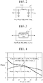
- FIG. 2 and 3 is a schematic diagram showing an example of the first phase adjustment circuit 13.
- the circuit configuration of the first phase adjustment circuit 13 is determined on the basis of the operating frequency band of the signal to be amplified.
- the first phase adjustment circuit 13 shown in Fig. 2 is implemented by a coil 13a and capacitors 13b and 13c.
- One end of the coil 13a is connected to the output side of the first auxiliary amplification element 7, and the other end of the coil 13a is connected to the input side of the second auxiliary amplification element 8.
- One end of the capacitor 13b is connected to each of the following parts: the output side of the first auxiliary amplification element 7 and the one end of the coil 13a, and the other end of the capacitor 13b is grounded.
- One end of the capacitor 13c is connected to each of the following parts: the input side of the second auxiliary amplification element 8 and the other end of the coil 13a, and the other end of the capacitor 13c is grounded.
- the first phase adjustment circuit 13 shown in Fig. 3 is implemented by a transmission line 13d.
- the configuration of the first phase adjustment circuit 13 shown by each of Figs. 2 and 3 is only an example, and the first phase adjustment circuit 13 may have a configuration different from that shown by each of Figs. 2 and 3 as long as the first phase adjustment circuit can change the phase characteristic at the time of the backoff operation while implementing the impedance matching at the time of the saturated operation.
- Fig. 4 is an explanatory drawing showing a result of simulation of a stability factor at the time of the backoff operation of the Doherty amplifier.
- a solid line shows the stability factor (Kfactor) at the time of the backoff operation of a conventional Doherty amplifier which does not include the first phase adjustment circuit 13.
- a broken line shows the stability factor at the time of the backoff operation of the Doherty amplifier shown in Fig. 1 .
- the operating frequency band of the signal to be amplified ranges from 25 to 31 GHz.
- the stability factor is equal to or less than 1 and thus its amplifying operation is unstable, depending on the operating frequency of the signal to be amplified.
- the stability factor is equal to or greater than 1 and thus its amplifying operation is stable over the entire operating frequency band.
- the Doherty amplifier includes: the first main amplification element 5 to amplify the first signal; the second main amplification element 6 to amplify the first signal amplified by the first main amplification element 5; the first auxiliary amplification element 7 to amplify the second signal; the second auxiliary amplification element 8 to amplify the second signal amplified by the first auxiliary amplification element 7; the combination circuit 9 to combine the first signal amplified by the second main amplification element 6 and the second signal amplified by the second auxiliary amplification element 8; and the first phase adjustment circuit 13 connected between the first auxiliary amplification element 7 and the second auxiliary amplification element 8.
- the Doherty amplifier is then configured in such a way that the first phase adjustment circuit 13 adjusts either the phase of a return signal going to the first auxiliary amplification element 7 as a result of passage of the first signal amplified by the second main amplification element 6 through the second auxiliary amplification element 8 as the return signal, or the phase of the return signal going to the second auxiliary amplification element 8 as a result of reflection of the return signal by the first auxiliary amplification element 7, at the time of the backoff operation of the second auxiliary amplification element 8, in such a way that the sum of the phase of the return signal going to the first auxiliary amplification element 7 and the phase of the return signal going to the second auxiliary amplification element 8 is not equal to 0 degrees in the operating frequency band of the first signal. Therefore, the Doherty amplifier can prevent an oscillation phenomenon occurring between the first auxiliary amplification element 7 and the second auxiliary amplification element 8.
- Embodiment 2 a Doherty amplifier including a main amplification element 20 that amplifies a signal to be amplified and outputs the amplified signal to a signal splitter circuit 2 will be explained.
- Fig. 5 is a schematic diagram showing the Doherty amplifier according to Embodiment 2.
- Fig. 5 because the same reference signs as those shown in Fig. 1 denote the same components or like components, an explanation of the components will be omitted.
- the main amplification element 20 is implemented by, for example, either an FET or an amplification circuit including an FET and an impedance conversion circuit.
- the main amplification element 20 is a carrier amplifier that operates in AB class, and amplifies a signal to be amplified and outputs the amplified signal to a signal splitter circuit 2.
- the Doherty amplifier shown in Fig. 5 is configured in such a way as to include the main amplification element 20 that amplifies the signal to be amplified and outputs the amplified signal to the signal splitter circuit 2. Therefore, the Doherty amplifier shown in Fig. 5 can prevent an oscillation phenomenon occurring between a first auxiliary amplification element 7 and a second auxiliary amplification element 8, like the Doherty amplifier shown in Fig. 1 . Further, the Doherty amplifier shown in Fig. 5 can increase the power of a composite signal to greater than that in the Doherty amplifier shown in Fig. 1 .
- the single main amplification element 20 is provided in a stage preceding the signal splitter circuit 2.
- Embodiment 3 a Doherty amplifier including a first signal generator 21 and a second signal generator 22 will be explained.
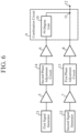
- Fig. 6 is a schematic diagram showing the Doherty amplifier according to Embodiment 3.
- Fig. 6 because the same reference signs as those shown in Fig. 1 denote the same components or like components, an explanation of the components will be omitted.
- the first signal generator 21 generates a first signal, and can change each of the following quantities: the frequency and amplitude of the first signal. Further, the first signal generator 21 can synchronize the phase of the first signal with a reference phase.
- the first signal generator 21 outputs the first signal whose phase is synchronized with the reference phase to a first main amplification element 5.
- the second signal generator 22 generates a second signal, and can change each of the following quantities: the frequency and amplitude of the second signal.
- the second signal generator 22 outputs the second signal whose phase lags 90 degrees behind the phase of the first signal outputted from the first signal generator 21 to a first auxiliary amplification element 7.
- the first signal outputted from the first signal generator 21 and the second signal outputted from the second signal generator 22 have the same amplitude.
- the Doherty amplifier shown in Fig. 6 includes the first signal generator 21 and the second signal generator 22 instead of the signal splitter circuit 2 shown in Fig. 1 .
- the first signal outputted from the first signal generator 21 to the first main amplification element 5 is the same as the first signal outputted from the signal splitter circuit 2 to the first main amplification element 5. Further, the second signal outputted from the second signal generator 22 to the first auxiliary amplification element 7 is the same as the second signal outputted from the signal splitter circuit 2 to the first auxiliary amplification element 7.
- the Doherty amplifier shown in Fig. 6 can prevent an oscillation phenomenon occurring between the first auxiliary amplification element 7 and a second auxiliary amplification element 8, like the Doherty amplifier shown in Fig. 1 .
- the present disclosure is suitable for Doherty amplifiers.
Landscapes
- Engineering & Computer Science (AREA)
- Power Engineering (AREA)
- Amplifiers (AREA)
Abstract
Description
- The present disclosure relates to a Doherty amplifier.
- Among Doherty amplifiers used as amplifiers for wireless communications, there are Doherty amplifiers in each of which two carrier amplifiers are connected in series and two peak amplifiers are connected in series.
- By the way, in a typical Doherty amplifier including a splitter circuit, a carrier amplifier, a peak amplifier and a combiner, a loop in which one of two signals into which a signal is split by the splitter circuit passes through each of the following circuits: the carrier amplifier, the combiner and the peak amplifier, and then returns to the splitter circuit may be formed. In order to suppress a loop oscillation which occurs because such a loop has a gain, there is a Doherty amplifier in which a splitter circuit includes a low pass filter which is a π type circuit and a high pass filter which is a T type circuit (for example, refer to Patent Literature 1).
- Patent Literature 1:
WO 2017/119062 - In conventional Doherty amplifiers in each of which two carrier amplifiers are connected in series and two peak amplifiers are connected in series, at a time of backoff operations of the peak amplifiers, a signal amplified by the two carrier amplifiers may pass through the peak amplifier on an output side, out of the two peak amplifiers, as a return signal. At this time, there is a problem that an oscillation phenomenon occurs in which the return signal which has passed through the peak amplifier on the output side is reflected by the other peak amplifier on an input side, and in which the return signal reflected by the other peak amplifier on the input side is further reflected by the peak amplifier on the output side.
- Even though the splitter circuit in the Doherty amplifier described in
Patent Literature 1 can prevent loop oscillations, the splitter circuit cannot be used to solve the above-mentioned problem. - According to the present disclosure, there is provided a Doherty amplifier including: a first main amplification element to amplify a first signal; a second main amplification element to amplify the first signal amplified by the first main amplification element; a first auxiliary amplification element to amplify a second signal; a second auxiliary amplification element to amplify the second signal amplified by the first auxiliary amplification element; a combination circuit to combine the first signal amplified by the second main amplification element and the second signal amplified by the second auxiliary amplification element; and a phase adjustment circuit connected between the first auxiliary amplification element and the second auxiliary amplification element, in which the phase adjustment circuit adjusts either a phase of a return signal going to the first auxiliary amplification element as a result of passage of the first signal amplified by the second main amplification element through the second auxiliary amplification element as the return signal, or a phase of the return signal going to the second auxiliary amplification element as a result of reflection of the return signal by the first auxiliary amplification element, at a time of a backoff operation of the second auxiliary amplification element, in such a way that a sum of the phase of the return signal going to the first auxiliary amplification element and the phase of the return signal going to the second auxiliary amplification element is not equal to 0 degrees in an operating frequency band of the first signal.
- According to the present disclosure, an oscillation phenomenon occurring between the first auxiliary amplification element and the second auxiliary amplification element can be prevented.
-
-
Fig. 1 is a schematic diagram showing a Doherty amplifier according toEmbodiment 1; -
Fig. 2 is a schematic diagram showing an example of a firstphase adjustment circuit 13; -
Fig. 3 is a schematic diagram showing an example of the firstphase adjustment circuit 13; -
Fig. 4 is an explanatory drawing showing a result of simulation of a stability factor at a time of a backoff operation of the Doherty amplifier; -
Fig. 5 is a schematic diagram showing a Doherty amplifier according toEmbodiment 2; and -
Fig. 6 is a schematic diagram showing a Doherty amplifier according toEmbodiment 3. - Hereinafter, in order to explain the present disclosure in greater detail, embodiments of the present disclosure will be explained with reference to the accompanying drawings.
-
Fig. 1 is a schematic diagram showing a Doherty amplifier according toEmbodiment 1. - In
Fig. 1 , aninput terminal 1 is one to which a signal to be amplified is supplied from the outside. - A
signal splitter circuit 2 includes a T-branch circuit 3 and asignal delay circuit 4. - The
signal splitter circuit 2 splits the signal to be amplified into two signals, and outputs one of the signals after split, as a first signal, to a firstmain amplification element 5. - The
signal splitter circuit 2 delays the phase of the other one of the signals after split by 90 degrees, and outputs the other signal whose phase is delayed by 90 degrees, as a second signal, to a first auxiliary amplification element 7. - The T-
branch circuit 3 splits the signal to be amplified into two signals, and outputs one of the signals after split, as a first signal, to the firstmain amplification element 5 and outputs the other one of the signals after split to thesignal delay circuit 4. - The
signal delay circuit 4 delays the phase of the other signal outputted from the T-branch circuit 3 by 90 degrees, and outputs the other signal whose phase is delayed by 90 degrees, as a second signal, to the first auxiliary amplification element 7. - In the Doherty amplifier shown in
Fig. 1 , thesignal splitter circuit 2 includes the T-branch circuit 3 and thesignal delay circuit 4. However, this is only an example, and thesignal splitter circuit 2 may include a Wilkinson power splitter circuit instead of the T-branch circuit 3, or may include a 90-degree hybrid circuit instead of the T-branch circuit 3 and thesignal delay circuit 4. - In the Doherty amplifier shown in
Fig. 1 , it is assumed that the one of the signals after split by the T-branch circuit 3 and the other one of the signals after split by the T-branch circuit 3 have the same amplitude. However, this is only an example, and the one of the signals after split by the T-branch circuit 3 and the other one of the signals after split by the T-branch circuit 3 may have different amplitudes. - Note that, to the
input terminal 1, a circuit such as an impedance conversion circuit or a phase circuit may be connected. - The first
main amplification element 5 is implemented by, for example, either a field effect transistor (FET) or an amplification circuit including an FET and an impedance conversion circuit. - The first
main amplification element 5 is a carrier amplifier that operates in AB class, and amplifies the first signal outputted from thesignal splitter circuit 2 and outputs the amplified first signal to a second main amplification element 6 via a secondphase adjustment circuit 14. - The second main amplification element 6 is implemented by, for example, either an FET or an amplification circuit including an FET and an impedance conversion circuit.
- The second main amplification element 6 is a carrier amplifier that operates in AB class, and further amplifies the first signal amplified by the first
main amplification element 5 and outputs the amplified first signal to acombination circuit 9. - The first auxiliary amplification element 7 is implemented by, for example, either an FET or an amplification circuit including an FET and an impedance conversion circuit.
- The first auxiliary amplification element 7 is a peak amplifier that operates in either B class or C class at a time of a backoff operation, and that operates in AB class at a time of a saturated operation.
- The first auxiliary amplification element 7 amplifies the second signal outputted from the
signal splitter circuit 2, and outputs the amplified second signal to a second auxiliary amplification element 8 via a firstphase adjustment circuit 13. - The time of the backoff operation is an operation when because the power of the second signal outputted from the
signal splitter circuit 2 is small, the output power of the first auxiliary amplification element 7 is lower than the output power of the firstmain amplification element 5. The time of the saturated operation is an operation when the output power of the first auxiliary amplification element 7 is the same as the output power of the firstmain amplification element 5. - The second auxiliary amplification element 8 is implemented by, for example, either an FET or an amplification circuit including an FET and an impedance conversion circuit.
- The second auxiliary amplification element 8 is a peak amplifier that operates in either B class or C class at a time of a backoff operation, and that operates in AB class at a time of a saturated operation.
- The second auxiliary amplification element 8 further amplifies the second signal amplified by the first auxiliary amplification element 7, and outputs the amplified second signal to the
combination circuit 9. - The time of the backoff operation is an operation when because the power of the second signal amplified by the first auxiliary amplification element 7 is small, the output power of the second auxiliary amplification element 8 is lower than the output power of the second main amplification element 6.
- The time of the saturated operation is an operation when the output power of the second auxiliary amplification element 8 is the same as the output power of the second main amplification element 6.
- The
combination circuit 9 includes a 90-degree line 10 and asignal combination point 11. - The
combination circuit 9 combines the first signal amplified by the second main amplification element 6 and the second signal amplified by the second auxiliary amplification element 8, and outputs a composite signal of the first signal and the second signal to anoutput terminal 12. - The 90-
degree line 10 is a circuit having an electric length of 90 degrees in the operating frequency band of the signal to be amplified. - At the
signal combination point 11, the first signal which has passed through the 90-degree line 10 and the second signal amplified by the second auxiliary amplification element 8 are combined. - In the Doherty amplifier shown in
Fig. 1 , thecombination circuit 9 includes the 90-degree line 10 and thesignal combination point 11. What is necessary for thecombination circuit 9 is just to be able to combine the first signal amplified by the second main amplification element 6 and the second signal amplified by the second auxiliary amplification element 8, and thecombination circuit 9 may be implemented by, for example, a lumped constant element, a distributed constant element, a π type circuit, a T type circuit, or a combination of those elements or circuits. - The
output terminal 12 is a terminal via which the composite signal outputted from thecombination circuit 9 is outputted to the outside. - Note that, to the
output terminal 12, a circuit such as an impedance conversion circuit or a phase circuit may be connected. - The first
phase adjustment circuit 13 is implemented by, for example, a lumped constant element, a distributed constant element, a π type circuit, a T type circuit, or a combination of those elements or circuits. - One end of the first
phase adjustment circuit 13 is connected to an output side of the first auxiliary amplification element 7, and the other end of the firstphase adjustment circuit 13 is connected to an input side of the second auxiliary amplification element 8. - At the time of the backoff operation of the second auxiliary amplification element 8, there is a case in which the first signal amplified by the second main amplification element 6 passes through the second auxiliary amplification element 8 as a return signal, and, as a result, the return signal goes to the first auxiliary amplification element 7. Further, there is a case in which the return signal is reflected by the first auxiliary amplification element 7, and, as a result, the return signal goes to the second auxiliary amplification element 8.
- The first
phase adjustment circuit 13 adjusts either the phase of the return signal going to the first auxiliary amplification element 7 or the phase of the return signal going to the second auxiliary amplification element 8 in such a way that the sum of the phase of the return signal going to the first auxiliary amplification element 7 and the phase of the return signal going to the second auxiliary amplification element 8 is not equal to 0 degrees in the operating frequency band of the first signal. - The first
phase adjustment circuit 13 acts as an impedance converter at the time of the saturated operation of the second auxiliary amplification element 8. - The second
phase adjustment circuit 14 is implemented by, for example, a lumped constant element, a distributed constant element, a π type circuit, a T type circuit, or a combination of those elements or circuits. - One end of the second
phase adjustment circuit 14 is connected to an output side of the firstmain amplification element 5, and the other end of the secondphase adjustment circuit 14 is connected to an input side of the second main amplification element 6. - The second
phase adjustment circuit 14 adjusts the phase of the first signal going from the firstmain amplification element 5 to the second main amplification element 6 in order to make the signal which reaches thesignal combination point 11 via the firstmain amplification element 5 from the T-branch circuit 3 be in phase with the signal which reaches thesignal combination point 11 via the first auxiliary amplification element 7 from the T-branch circuit 3. - Next, the operation of the Doherty amplifier shown in
Fig. 1 will be explained. - If the second auxiliary amplification element 8 which is a peak amplifier is an ideal transistor, the impedance of the second auxiliary amplification element is high at the time of the backoff operation. Therefore, the connection of the second auxiliary amplification element 8 to the
signal combination point 11 of thecombination circuit 9 is equivalently in a connectionless state. More specifically, an output side of the second auxiliary amplification element 8 serves as an open end equivalently. - However, because the second auxiliary amplification element 8 mounted in the Doherty amplifier shown in
Fig. 1 has an isolation characteristic, there is a case in which the impedance of the second auxiliary amplification element 8 is not high depending on the frequency f0 of the signal to be amplified. - In the case where the impedance of the second auxiliary amplification element 8 is not high at the time of the backoff operation of the second auxiliary amplification element 8, the first signal amplified by the second main amplification element 6 may pass through the second auxiliary amplification element 8 as a return signal.
- At this time, there may occur an oscillation phenomenon in which the return signal which has passed through the second auxiliary amplification element 8 is reflected by the first auxiliary amplification element 7, and the return signal reflected by the first auxiliary amplification element 7 is further reflected by the second auxiliary amplification element 8.
- In accordance with the Nyquist theorem, at the frequency where the sum of the phase of the return signal going to the first auxiliary amplification element 7 and the phase of the return signal going to the second auxiliary amplification element 8 is 0 degrees, the return signal has the maximum gain. When the return signal has the maximum gain, the above-mentioned oscillation phenomenon is maximized.
- In order to prevent the above-mentioned oscillation phenomenon, the first
phase adjustment circuit 13 adjusts either the phase of the return signal going to the first auxiliary amplification element 7 or the phase of the return signal going to the second auxiliary amplification element 8 in such a way that the sum of the phase of the return signal going to the first auxiliary amplification element 7 and the phase of the return signal going to the second auxiliary amplification element 8 is not equal to 0 degrees at the frequency f0 of the signal to be amplified. - It is assumed that the phase of the return signal going to the second auxiliary amplification element 8 is, for example, within a range of +45 degrees to +65 degrees in the operating frequency band of the signal to be amplified. In this case, the first
phase adjustment circuit 13 adjusts the phase of the return signal going to the first auxiliary amplification element 7 in such a way that the phase of the return signal going to the first auxiliary amplification element 7 does not fall within a range of -45 degrees to -65 degrees. - In the Doherty amplifier shown in
Fig. 1 , the firstphase adjustment circuit 13 adjusting either the phase of the return signal going to the first auxiliary amplification element 7 or the phase of the return signal going to the second auxiliary amplification element 8 in such a way that the sum of the phase of the return signal going to the first auxiliary amplification element 7 and the phase of the return signal going to the second auxiliary amplification element 8 is not equal to 0 degrees. What is necessary is just to make the sum of the phase of the return signal going to the first auxiliary amplification element 7 and the phase of the return signal going to the second auxiliary amplification element 8 be not 0 degrees. Therefore, the firstphase adjustment circuit 13 may adjust either the phase of the return signal going to the first auxiliary amplification element 7 or the phase of the return signal going to the second auxiliary amplification element 8 in such a way that the sum does not fall within a range of -5 degrees to +5 degrees, for example. - In the Doherty amplifier shown in
Fig. 1 , the firstphase adjustment circuit 13 has a characteristic impedance of the same value as the output impedance of the first auxiliary amplification element 7 at the time of the saturated operation or the input impedance of the second auxiliary amplification element 8 at the time of the saturated operation. - Because the first
phase adjustment circuit 13 has the above-mentioned characteristic impedance, the first phase adjustment circuit can change only the phase characteristic at the time of the backoff operation without having an influence on the impedance matching at the time of the saturated operation. - It is assumed that the input impedance of the second auxiliary amplification element 8 at the time of the saturated operation is, for example, 50 Ω, and the phase of the return signal going to the second auxiliary amplification element 8 is within a range of +45 degrees to +65 degrees, for example. In this case, the first
phase adjustment circuit 13 has a circuit configuration in which the first phase adjustment circuit has a characteristic impedance of 50 Ω and has a phase characteristic where the phase of the return signal going to the first auxiliary amplification element 7 is outside a range of -45 degrees to -65 degrees. - Each of
Figs. 2 and 3 is a schematic diagram showing an example of the firstphase adjustment circuit 13. - The circuit configuration of the first
phase adjustment circuit 13 is determined on the basis of the operating frequency band of the signal to be amplified. - The first
phase adjustment circuit 13 shown inFig. 2 is implemented by acoil 13a andcapacitors - One end of the
coil 13a is connected to the output side of the first auxiliary amplification element 7, and the other end of thecoil 13a is connected to the input side of the second auxiliary amplification element 8. - One end of the
capacitor 13b is connected to each of the following parts: the output side of the first auxiliary amplification element 7 and the one end of thecoil 13a, and the other end of thecapacitor 13b is grounded. - One end of the
capacitor 13c is connected to each of the following parts: the input side of the second auxiliary amplification element 8 and the other end of thecoil 13a, and the other end of thecapacitor 13c is grounded. - The first
phase adjustment circuit 13 shown inFig. 3 is implemented by atransmission line 13d. - The configuration of the first
phase adjustment circuit 13 shown by each ofFigs. 2 and 3 is only an example, and the firstphase adjustment circuit 13 may have a configuration different from that shown by each ofFigs. 2 and 3 as long as the first phase adjustment circuit can change the phase characteristic at the time of the backoff operation while implementing the impedance matching at the time of the saturated operation. -
Fig. 4 is an explanatory drawing showing a result of simulation of a stability factor at the time of the backoff operation of the Doherty amplifier. - In
Fig. 4 , a solid line shows the stability factor (Kfactor) at the time of the backoff operation of a conventional Doherty amplifier which does not include the firstphase adjustment circuit 13. A broken line shows the stability factor at the time of the backoff operation of the Doherty amplifier shown inFig. 1 . - The operating frequency band of the signal to be amplified ranges from 25 to 31 GHz.
- In the conventional Doherty amplifier, the stability factor is equal to or less than 1 and thus its amplifying operation is unstable, depending on the operating frequency of the signal to be amplified.
- In the Doherty amplifier shown in
Fig. 1 , the stability factor is equal to or greater than 1 and thus its amplifying operation is stable over the entire operating frequency band. - In above-mentioned
Embodiment 1, the Doherty amplifier includes: the firstmain amplification element 5 to amplify the first signal; the second main amplification element 6 to amplify the first signal amplified by the firstmain amplification element 5; the first auxiliary amplification element 7 to amplify the second signal; the second auxiliary amplification element 8 to amplify the second signal amplified by the first auxiliary amplification element 7; thecombination circuit 9 to combine the first signal amplified by the second main amplification element 6 and the second signal amplified by the second auxiliary amplification element 8; and the firstphase adjustment circuit 13 connected between the first auxiliary amplification element 7 and the second auxiliary amplification element 8. The Doherty amplifier is then configured in such a way that the firstphase adjustment circuit 13 adjusts either the phase of a return signal going to the first auxiliary amplification element 7 as a result of passage of the first signal amplified by the second main amplification element 6 through the second auxiliary amplification element 8 as the return signal, or the phase of the return signal going to the second auxiliary amplification element 8 as a result of reflection of the return signal by the first auxiliary amplification element 7, at the time of the backoff operation of the second auxiliary amplification element 8, in such a way that the sum of the phase of the return signal going to the first auxiliary amplification element 7 and the phase of the return signal going to the second auxiliary amplification element 8 is not equal to 0 degrees in the operating frequency band of the first signal. Therefore, the Doherty amplifier can prevent an oscillation phenomenon occurring between the first auxiliary amplification element 7 and the second auxiliary amplification element 8. - In
Embodiment 2, a Doherty amplifier including amain amplification element 20 that amplifies a signal to be amplified and outputs the amplified signal to asignal splitter circuit 2 will be explained. -
Fig. 5 is a schematic diagram showing the Doherty amplifier according toEmbodiment 2. InFig. 5 , because the same reference signs as those shown inFig. 1 denote the same components or like components, an explanation of the components will be omitted. - The
main amplification element 20 is implemented by, for example, either an FET or an amplification circuit including an FET and an impedance conversion circuit. - The
main amplification element 20 is a carrier amplifier that operates in AB class, and amplifies a signal to be amplified and outputs the amplified signal to asignal splitter circuit 2. - In
Embodiment 2, the Doherty amplifier shown inFig. 5 is configured in such a way as to include themain amplification element 20 that amplifies the signal to be amplified and outputs the amplified signal to thesignal splitter circuit 2. Therefore, the Doherty amplifier shown inFig. 5 can prevent an oscillation phenomenon occurring between a first auxiliary amplification element 7 and a second auxiliary amplification element 8, like the Doherty amplifier shown inFig. 1 . Further, the Doherty amplifier shown inFig. 5 can increase the power of a composite signal to greater than that in the Doherty amplifier shown inFig. 1 . - In the Doherty amplifier shown in
Fig. 5 , the singlemain amplification element 20 is provided in a stage preceding thesignal splitter circuit 2. However, this is only an example, and multiplemain amplification elements 20 may be connected in series in a stage preceding thesignal splitter circuit 2. - In
Embodiment 3, a Doherty amplifier including afirst signal generator 21 and asecond signal generator 22 will be explained. -
Fig. 6 is a schematic diagram showing the Doherty amplifier according toEmbodiment 3. InFig. 6 , because the same reference signs as those shown inFig. 1 denote the same components or like components, an explanation of the components will be omitted. - The
first signal generator 21 generates a first signal, and can change each of the following quantities: the frequency and amplitude of the first signal. Further, thefirst signal generator 21 can synchronize the phase of the first signal with a reference phase. - The
first signal generator 21 outputs the first signal whose phase is synchronized with the reference phase to a firstmain amplification element 5. - The
second signal generator 22 generates a second signal, and can change each of the following quantities: the frequency and amplitude of the second signal. - The
second signal generator 22 outputs the second signal whose phase lags 90 degrees behind the phase of the first signal outputted from thefirst signal generator 21 to a first auxiliary amplification element 7. - In the Doherty amplifier shown in
Fig. 6 , it is assumed that the first signal outputted from thefirst signal generator 21 and the second signal outputted from thesecond signal generator 22 have the same amplitude. However, this is only an example, and the first signal outputted from thefirst signal generator 21 and the second signal outputted from thesecond signal generator 22 may have different amplitudes. - The Doherty amplifier shown in
Fig. 6 includes thefirst signal generator 21 and thesecond signal generator 22 instead of thesignal splitter circuit 2 shown inFig. 1 . - The first signal outputted from the
first signal generator 21 to the firstmain amplification element 5 is the same as the first signal outputted from thesignal splitter circuit 2 to the firstmain amplification element 5. Further, the second signal outputted from thesecond signal generator 22 to the first auxiliary amplification element 7 is the same as the second signal outputted from thesignal splitter circuit 2 to the first auxiliary amplification element 7. - Therefore, the Doherty amplifier shown in
Fig. 6 can prevent an oscillation phenomenon occurring between the first auxiliary amplification element 7 and a second auxiliary amplification element 8, like the Doherty amplifier shown inFig. 1 . - It is to be understood that an arbitrary combination of two or more of the above-mentioned embodiments can be made, various changes can be made in an arbitrary component according to any one of the above-mentioned embodiments, or an arbitrary component according to any one of the above-mentioned embodiments can be omitted.
- The present disclosure is suitable for Doherty amplifiers.
- 1 input terminal, 2 signal splitter circuit, 3 T-branch circuit, 4 signal delay circuit, 5 first main amplification element, 6 second main amplification element, 7 first auxiliary amplification element, 8 second auxiliary amplification element, 9 combination circuit, 10 90-degree line, 11 signal combination point, 12 output terminal, 13 first phase adjustment circuit, 13a coil, 13b, 13c capacitor, 13d transmission line, 14 second phase adjustment circuit, 20 main amplification element, 21 first signal generator, and 22 second signal generator.
Claims (4)
- A Doherty amplifier comprising:a first main amplification element to amplify a first signal;a second main amplification element to amplify the first signal amplified by the first main amplification element;a first auxiliary amplification element to amplify a second signal;a second auxiliary amplification element to amplify the second signal amplified by the first auxiliary amplification element;a combination circuit to combine the first signal amplified by the second main amplification element and the second signal amplified by the second auxiliary amplification element; anda phase adjustment circuit connected between the first auxiliary amplification element and the second auxiliary amplification element,wherein the phase adjustment circuit adjusts either a phase of a return signal going to the first auxiliary amplification element as a result of passage of the first signal amplified by the second main amplification element through the second auxiliary amplification element as the return signal, or a phase of the return signal going to the second auxiliary amplification element as a result of reflection of the return signal by the first auxiliary amplification element, at a time of a backoff operation of the second auxiliary amplification element, in such a way that a sum of the phase of the return signal going to the first auxiliary amplification element and the phase of the return signal going to the second auxiliary amplification element is not equal to 0 degrees in an operating frequency band of the first signal.
- The Doherty amplifier according to claim 1, wherein the Doherty amplifier comprises a signal splitter circuit to split a signal into two signals, output one of the signals after split, as the first signal, to the first main amplification element, delay a phase of the other one of the signals after split by 90 degrees, and output the other signal whose phase is delayed by 90 degrees, as the second signal, to the first auxiliary amplification element.
- The Doherty amplifier according to claim 2, wherein the Doherty amplifier comprises a main amplification element to amplify a signal to be amplified and output the amplified signal to the signal splitter circuit.
- The Doherty amplifier according to claim 1, wherein the Doherty amplifier comprises a first signal generator to output the first signal to the first main amplification element, and a second signal generator to output the second signal whose phase lags 90 degrees behind a phase of the first signal outputted from the first signal generator to the first auxiliary amplification element.
Applications Claiming Priority (1)
| Application Number | Priority Date | Filing Date | Title |
|---|---|---|---|
| PCT/JP2020/024778 WO2021260828A1 (en) | 2020-06-24 | 2020-06-24 | Doherty amplifier |
Publications (3)
| Publication Number | Publication Date |
|---|---|
| EP4156508A1 true EP4156508A1 (en) | 2023-03-29 |
| EP4156508A4 EP4156508A4 (en) | 2023-07-19 |
| EP4156508B1 EP4156508B1 (en) | 2024-08-21 |
Family
ID=79282595
Family Applications (1)
| Application Number | Title | Priority Date | Filing Date |
|---|---|---|---|
| EP20941985.2A Active EP4156508B1 (en) | 2020-06-24 | 2020-06-24 | Doherty amplifier |
Country Status (5)
| Country | Link |
|---|---|
| US (1) | US20230048682A1 (en) |
| EP (1) | EP4156508B1 (en) |
| JP (1) | JP7166491B2 (en) |
| CN (1) | CN115804007A (en) |
| WO (1) | WO2021260828A1 (en) |
Families Citing this family (1)
| Publication number | Priority date | Publication date | Assignee | Title |
|---|---|---|---|---|
| JP7670044B2 (en) | 2022-11-15 | 2025-04-30 | 株式会社村田製作所 | Power Amplifiers |
Family Cites Families (10)
| Publication number | Priority date | Publication date | Assignee | Title |
|---|---|---|---|---|
| CN101582682B (en) * | 2009-06-12 | 2011-12-28 | 华为技术有限公司 | Power amplifier and transmitter |
| JP2013090037A (en) * | 2011-10-14 | 2013-05-13 | Mitsubishi Electric Corp | High frequency signal amplifier |
| WO2014108716A1 (en) * | 2013-01-10 | 2014-07-17 | Freescale Semiconductor, Inc. | Doherty amplifier |
| JP6384105B2 (en) * | 2014-04-22 | 2018-09-05 | 三菱電機株式会社 | Power amplifier |
| US9450541B2 (en) * | 2014-05-13 | 2016-09-20 | Skyworks Solutions, Inc. | Systems and methods related to linear and efficient broadband power amplifiers |
| JP5913442B2 (en) * | 2014-06-18 | 2016-04-27 | 住友電工デバイス・イノベーション株式会社 | Doherty amplifier |
| US10340855B2 (en) | 2016-01-05 | 2019-07-02 | Mitsubishi Electric Corporation | Doherty amplifier |
| US10778156B2 (en) * | 2017-06-20 | 2020-09-15 | Infineon Technologies Ag | Interstage matching network |
| US20200136564A1 (en) * | 2017-07-27 | 2020-04-30 | Mitsubishi Electric Corporation | Doherty amplifier and amplification circuit |
| JP6861908B2 (en) * | 2018-11-30 | 2021-04-21 | 三菱電機株式会社 | Transmitter |
-
2020
- 2020-06-24 WO PCT/JP2020/024778 patent/WO2021260828A1/en not_active Ceased
- 2020-06-24 EP EP20941985.2A patent/EP4156508B1/en active Active
- 2020-06-24 CN CN202080102026.0A patent/CN115804007A/en active Pending
- 2020-06-24 JP JP2022531303A patent/JP7166491B2/en active Active
-
2022
- 2022-11-02 US US17/979,251 patent/US20230048682A1/en not_active Abandoned
Also Published As
| Publication number | Publication date |
|---|---|
| US20230048682A1 (en) | 2023-02-16 |
| EP4156508B1 (en) | 2024-08-21 |
| EP4156508A4 (en) | 2023-07-19 |
| JP7166491B2 (en) | 2022-11-07 |
| CN115804007A (en) | 2023-03-14 |
| WO2021260828A1 (en) | 2021-12-30 |
| JPWO2021260828A1 (en) | 2021-12-30 |
Similar Documents
| Publication | Publication Date | Title |
|---|---|---|
| JP4027988B2 (en) | Multistage high efficiency linear power amplifier and method | |
| US6538509B2 (en) | Linearizer for a power amplifier | |
| US4926136A (en) | Power amplifier combiner for improving linearity of an output | |
| US6242979B1 (en) | Linearization using parallel cancellation in linear power amplifier | |
| EP3700087B1 (en) | Doherty amplifier and doherty amplifier circuit | |
| US5576660A (en) | Broadband predistortion linearizer with automatic temperature compensation for microwave amplifiers | |
| US10340855B2 (en) | Doherty amplifier | |
| JPH0878965A (en) | Feed forward amplifier | |
| US20220239259A1 (en) | Doherty amplifier and communication device | |
| US8023908B2 (en) | Intermodulation signal generator of power amplifier and pre-distortion linearizer having the same | |
| US20230048682A1 (en) | Doherty amplifier | |
| US6744314B2 (en) | Wideband power amplifier linearization technique | |
| US6198346B1 (en) | Adaptive linear amplifier without output power loss | |
| JP2003198273A (en) | Amplifier circuit | |
| US6392481B1 (en) | Method and apparatus for improved fed forward amplification | |
| JP2003332852A (en) | Pre-distortion circuit | |
| JP2006339888A (en) | High frequency amplifier circuit | |
| RU2178946C2 (en) | Nonlinear distortion corrector | |
| US20030020541A1 (en) | Feedforward amplifier and feedforward amplification method | |
| KR950003278B1 (en) | Feed-Forward Linearization Circuit of Power Amplifiers | |
| KR100858063B1 (en) | Doherty Amplifier | |
| JP2006074699A (en) | Distortion generation circuit and distortion compensation apparatus | |
| EP4148989A1 (en) | Amplification circuit | |
| WO2024257289A1 (en) | Balance-type amplifier | |
| JP2025095451A (en) | Amplification circuit |
Legal Events
| Date | Code | Title | Description |
|---|---|---|---|
| STAA | Information on the status of an ep patent application or granted ep patent |
Free format text: STATUS: THE INTERNATIONAL PUBLICATION HAS BEEN MADE |
|
| PUAI | Public reference made under article 153(3) epc to a published international application that has entered the european phase |
Free format text: ORIGINAL CODE: 0009012 |
|
| STAA | Information on the status of an ep patent application or granted ep patent |
Free format text: STATUS: REQUEST FOR EXAMINATION WAS MADE |
|
| 17P | Request for examination filed |
Effective date: 20221213 |
|
| AK | Designated contracting states |
Kind code of ref document: A1 Designated state(s): AL AT BE BG CH CY CZ DE DK EE ES FI FR GB GR HR HU IE IS IT LI LT LU LV MC MK MT NL NO PL PT RO RS SE SI SK SM TR |
|
| A4 | Supplementary search report drawn up and despatched |
Effective date: 20230619 |
|
| RIC1 | Information provided on ipc code assigned before grant |
Ipc: H03F 3/60 20060101ALI20230613BHEP Ipc: H03F 1/56 20060101ALI20230613BHEP Ipc: H03F 1/02 20060101AFI20230613BHEP |
|
| DAV | Request for validation of the european patent (deleted) | ||
| DAX | Request for extension of the european patent (deleted) | ||
| REG | Reference to a national code |
Ref country code: DE Ref legal event code: R079 Free format text: PREVIOUS MAIN CLASS: H03F0001020000 Ipc: H03F0001420000 Ref country code: DE Ref legal event code: R079 Ref document number: 602020036470 Country of ref document: DE Free format text: PREVIOUS MAIN CLASS: H03F0001020000 Ipc: H03F0001420000 |
|
| GRAP | Despatch of communication of intention to grant a patent |
Free format text: ORIGINAL CODE: EPIDOSNIGR1 |
|
| STAA | Information on the status of an ep patent application or granted ep patent |
Free format text: STATUS: GRANT OF PATENT IS INTENDED |
|
| RIC1 | Information provided on ipc code assigned before grant |
Ipc: H03F 3/60 20060101ALI20240304BHEP Ipc: H03F 1/56 20060101ALI20240304BHEP Ipc: H03F 1/02 20060101ALI20240304BHEP Ipc: H03F 1/42 20060101AFI20240304BHEP |
|
| INTG | Intention to grant announced |
Effective date: 20240328 |
|
| GRAS | Grant fee paid |
Free format text: ORIGINAL CODE: EPIDOSNIGR3 |
|
| GRAA | (expected) grant |
Free format text: ORIGINAL CODE: 0009210 |
|
| STAA | Information on the status of an ep patent application or granted ep patent |
Free format text: STATUS: THE PATENT HAS BEEN GRANTED |
|
| AK | Designated contracting states |
Kind code of ref document: B1 Designated state(s): AL AT BE BG CH CY CZ DE DK EE ES FI FR GB GR HR HU IE IS IT LI LT LU LV MC MK MT NL NO PL PT RO RS SE SI SK SM TR |
|
| REG | Reference to a national code |
Ref country code: GB Ref legal event code: FG4D |
|
| REG | Reference to a national code |
Ref country code: CH Ref legal event code: EP |
|
| REG | Reference to a national code |
Ref country code: IE Ref legal event code: FG4D |
|
| REG | Reference to a national code |
Ref country code: DE Ref legal event code: R096 Ref document number: 602020036470 Country of ref document: DE |
|
| REG | Reference to a national code |
Ref country code: LT Ref legal event code: MG9D |
|
| REG | Reference to a national code |
Ref country code: NL Ref legal event code: MP Effective date: 20240821 |
|
| PG25 | Lapsed in a contracting state [announced via postgrant information from national office to epo] |
Ref country code: NO Free format text: LAPSE BECAUSE OF FAILURE TO SUBMIT A TRANSLATION OF THE DESCRIPTION OR TO PAY THE FEE WITHIN THE PRESCRIBED TIME-LIMIT Effective date: 20241121 |
|
| REG | Reference to a national code |
Ref country code: AT Ref legal event code: MK05 Ref document number: 1716519 Country of ref document: AT Kind code of ref document: T Effective date: 20240821 |
|
| PG25 | Lapsed in a contracting state [announced via postgrant information from national office to epo] |
Ref country code: NL Free format text: LAPSE BECAUSE OF FAILURE TO SUBMIT A TRANSLATION OF THE DESCRIPTION OR TO PAY THE FEE WITHIN THE PRESCRIBED TIME-LIMIT Effective date: 20240821 Ref country code: GR Free format text: LAPSE BECAUSE OF FAILURE TO SUBMIT A TRANSLATION OF THE DESCRIPTION OR TO PAY THE FEE WITHIN THE PRESCRIBED TIME-LIMIT Effective date: 20241122 Ref country code: FI Free format text: LAPSE BECAUSE OF FAILURE TO SUBMIT A TRANSLATION OF THE DESCRIPTION OR TO PAY THE FEE WITHIN THE PRESCRIBED TIME-LIMIT Effective date: 20240821 Ref country code: PT Free format text: LAPSE BECAUSE OF FAILURE TO SUBMIT A TRANSLATION OF THE DESCRIPTION OR TO PAY THE FEE WITHIN THE PRESCRIBED TIME-LIMIT Effective date: 20241223 Ref country code: PL Free format text: LAPSE BECAUSE OF FAILURE TO SUBMIT A TRANSLATION OF THE DESCRIPTION OR TO PAY THE FEE WITHIN THE PRESCRIBED TIME-LIMIT Effective date: 20240821 |
|
| PG25 | Lapsed in a contracting state [announced via postgrant information from national office to epo] |
Ref country code: BG Free format text: LAPSE BECAUSE OF FAILURE TO SUBMIT A TRANSLATION OF THE DESCRIPTION OR TO PAY THE FEE WITHIN THE PRESCRIBED TIME-LIMIT Effective date: 20240821 |
|
| PG25 | Lapsed in a contracting state [announced via postgrant information from national office to epo] |
Ref country code: LV Free format text: LAPSE BECAUSE OF FAILURE TO SUBMIT A TRANSLATION OF THE DESCRIPTION OR TO PAY THE FEE WITHIN THE PRESCRIBED TIME-LIMIT Effective date: 20240821 |
|
| PG25 | Lapsed in a contracting state [announced via postgrant information from national office to epo] |
Ref country code: IS Free format text: LAPSE BECAUSE OF FAILURE TO SUBMIT A TRANSLATION OF THE DESCRIPTION OR TO PAY THE FEE WITHIN THE PRESCRIBED TIME-LIMIT Effective date: 20241221 Ref country code: AT Free format text: LAPSE BECAUSE OF FAILURE TO SUBMIT A TRANSLATION OF THE DESCRIPTION OR TO PAY THE FEE WITHIN THE PRESCRIBED TIME-LIMIT Effective date: 20240821 |
|
| PG25 | Lapsed in a contracting state [announced via postgrant information from national office to epo] |
Ref country code: HR Free format text: LAPSE BECAUSE OF FAILURE TO SUBMIT A TRANSLATION OF THE DESCRIPTION OR TO PAY THE FEE WITHIN THE PRESCRIBED TIME-LIMIT Effective date: 20240821 |
|
| PG25 | Lapsed in a contracting state [announced via postgrant information from national office to epo] |
Ref country code: ES Free format text: LAPSE BECAUSE OF FAILURE TO SUBMIT A TRANSLATION OF THE DESCRIPTION OR TO PAY THE FEE WITHIN THE PRESCRIBED TIME-LIMIT Effective date: 20240821 Ref country code: RS Free format text: LAPSE BECAUSE OF FAILURE TO SUBMIT A TRANSLATION OF THE DESCRIPTION OR TO PAY THE FEE WITHIN THE PRESCRIBED TIME-LIMIT Effective date: 20241121 |
|
| PG25 | Lapsed in a contracting state [announced via postgrant information from national office to epo] |
Ref country code: RS Free format text: LAPSE BECAUSE OF FAILURE TO SUBMIT A TRANSLATION OF THE DESCRIPTION OR TO PAY THE FEE WITHIN THE PRESCRIBED TIME-LIMIT Effective date: 20241121 Ref country code: PT Free format text: LAPSE BECAUSE OF FAILURE TO SUBMIT A TRANSLATION OF THE DESCRIPTION OR TO PAY THE FEE WITHIN THE PRESCRIBED TIME-LIMIT Effective date: 20241223 Ref country code: PL Free format text: LAPSE BECAUSE OF FAILURE TO SUBMIT A TRANSLATION OF THE DESCRIPTION OR TO PAY THE FEE WITHIN THE PRESCRIBED TIME-LIMIT Effective date: 20240821 Ref country code: NO Free format text: LAPSE BECAUSE OF FAILURE TO SUBMIT A TRANSLATION OF THE DESCRIPTION OR TO PAY THE FEE WITHIN THE PRESCRIBED TIME-LIMIT Effective date: 20241121 Ref country code: NL Free format text: LAPSE BECAUSE OF FAILURE TO SUBMIT A TRANSLATION OF THE DESCRIPTION OR TO PAY THE FEE WITHIN THE PRESCRIBED TIME-LIMIT Effective date: 20240821 Ref country code: LV Free format text: LAPSE BECAUSE OF FAILURE TO SUBMIT A TRANSLATION OF THE DESCRIPTION OR TO PAY THE FEE WITHIN THE PRESCRIBED TIME-LIMIT Effective date: 20240821 Ref country code: IS Free format text: LAPSE BECAUSE OF FAILURE TO SUBMIT A TRANSLATION OF THE DESCRIPTION OR TO PAY THE FEE WITHIN THE PRESCRIBED TIME-LIMIT Effective date: 20241221 Ref country code: HR Free format text: LAPSE BECAUSE OF FAILURE TO SUBMIT A TRANSLATION OF THE DESCRIPTION OR TO PAY THE FEE WITHIN THE PRESCRIBED TIME-LIMIT Effective date: 20240821 Ref country code: GR Free format text: LAPSE BECAUSE OF FAILURE TO SUBMIT A TRANSLATION OF THE DESCRIPTION OR TO PAY THE FEE WITHIN THE PRESCRIBED TIME-LIMIT Effective date: 20241122 Ref country code: FI Free format text: LAPSE BECAUSE OF FAILURE TO SUBMIT A TRANSLATION OF THE DESCRIPTION OR TO PAY THE FEE WITHIN THE PRESCRIBED TIME-LIMIT Effective date: 20240821 Ref country code: ES Free format text: LAPSE BECAUSE OF FAILURE TO SUBMIT A TRANSLATION OF THE DESCRIPTION OR TO PAY THE FEE WITHIN THE PRESCRIBED TIME-LIMIT Effective date: 20240821 Ref country code: BG Free format text: LAPSE BECAUSE OF FAILURE TO SUBMIT A TRANSLATION OF THE DESCRIPTION OR TO PAY THE FEE WITHIN THE PRESCRIBED TIME-LIMIT Effective date: 20240821 Ref country code: AT Free format text: LAPSE BECAUSE OF FAILURE TO SUBMIT A TRANSLATION OF THE DESCRIPTION OR TO PAY THE FEE WITHIN THE PRESCRIBED TIME-LIMIT Effective date: 20240821 |
|
| PG25 | Lapsed in a contracting state [announced via postgrant information from national office to epo] |
Ref country code: SM Free format text: LAPSE BECAUSE OF FAILURE TO SUBMIT A TRANSLATION OF THE DESCRIPTION OR TO PAY THE FEE WITHIN THE PRESCRIBED TIME-LIMIT Effective date: 20240821 Ref country code: RO Free format text: LAPSE BECAUSE OF FAILURE TO SUBMIT A TRANSLATION OF THE DESCRIPTION OR TO PAY THE FEE WITHIN THE PRESCRIBED TIME-LIMIT Effective date: 20240821 Ref country code: DK Free format text: LAPSE BECAUSE OF FAILURE TO SUBMIT A TRANSLATION OF THE DESCRIPTION OR TO PAY THE FEE WITHIN THE PRESCRIBED TIME-LIMIT Effective date: 20240821 |
|
| PG25 | Lapsed in a contracting state [announced via postgrant information from national office to epo] |
Ref country code: EE Free format text: LAPSE BECAUSE OF FAILURE TO SUBMIT A TRANSLATION OF THE DESCRIPTION OR TO PAY THE FEE WITHIN THE PRESCRIBED TIME-LIMIT Effective date: 20240821 |
|
| PG25 | Lapsed in a contracting state [announced via postgrant information from national office to epo] |
Ref country code: CZ Free format text: LAPSE BECAUSE OF FAILURE TO SUBMIT A TRANSLATION OF THE DESCRIPTION OR TO PAY THE FEE WITHIN THE PRESCRIBED TIME-LIMIT Effective date: 20240821 |
|
| PG25 | Lapsed in a contracting state [announced via postgrant information from national office to epo] |
Ref country code: SK Free format text: LAPSE BECAUSE OF FAILURE TO SUBMIT A TRANSLATION OF THE DESCRIPTION OR TO PAY THE FEE WITHIN THE PRESCRIBED TIME-LIMIT Effective date: 20240821 Ref country code: IT Free format text: LAPSE BECAUSE OF FAILURE TO SUBMIT A TRANSLATION OF THE DESCRIPTION OR TO PAY THE FEE WITHIN THE PRESCRIBED TIME-LIMIT Effective date: 20240821 |
|
| REG | Reference to a national code |
Ref country code: DE Ref legal event code: R097 Ref document number: 602020036470 Country of ref document: DE |
|
| PLBE | No opposition filed within time limit |
Free format text: ORIGINAL CODE: 0009261 |
|
| STAA | Information on the status of an ep patent application or granted ep patent |
Free format text: STATUS: NO OPPOSITION FILED WITHIN TIME LIMIT |
|
| PGFP | Annual fee paid to national office [announced via postgrant information from national office to epo] |
Ref country code: DE Payment date: 20250429 Year of fee payment: 6 |
|
| PGFP | Annual fee paid to national office [announced via postgrant information from national office to epo] |
Ref country code: GB Payment date: 20250501 Year of fee payment: 6 |
|
| PGFP | Annual fee paid to national office [announced via postgrant information from national office to epo] |
Ref country code: FR Payment date: 20250508 Year of fee payment: 6 |
|
| 26N | No opposition filed |
Effective date: 20250522 |
|
| PG25 | Lapsed in a contracting state [announced via postgrant information from national office to epo] |
Ref country code: SE Free format text: LAPSE BECAUSE OF FAILURE TO SUBMIT A TRANSLATION OF THE DESCRIPTION OR TO PAY THE FEE WITHIN THE PRESCRIBED TIME-LIMIT Effective date: 20240821 |
|
| P01 | Opt-out of the competence of the unified patent court (upc) registered |
Free format text: CASE NUMBER: UPC_APP_4946_4156508/2025 Effective date: 20250827 |
|
| REG | Reference to a national code |
Ref country code: CH Ref legal event code: H13 Free format text: ST27 STATUS EVENT CODE: U-0-0-H10-H13 (AS PROVIDED BY THE NATIONAL OFFICE) Effective date: 20260127 |
|
| PG25 | Lapsed in a contracting state [announced via postgrant information from national office to epo] |
Ref country code: MC Free format text: LAPSE BECAUSE OF FAILURE TO SUBMIT A TRANSLATION OF THE DESCRIPTION OR TO PAY THE FEE WITHIN THE PRESCRIBED TIME-LIMIT Effective date: 20240821 |
|
| PG25 | Lapsed in a contracting state [announced via postgrant information from national office to epo] |
Ref country code: LU Free format text: LAPSE BECAUSE OF NON-PAYMENT OF DUE FEES Effective date: 20250624 |
|
| REG | Reference to a national code |
Ref country code: BE Ref legal event code: MM Effective date: 20250630 |
|
| PG25 | Lapsed in a contracting state [announced via postgrant information from national office to epo] |
Ref country code: IE Free format text: LAPSE BECAUSE OF NON-PAYMENT OF DUE FEES Effective date: 20250624 |
|
| PG25 | Lapsed in a contracting state [announced via postgrant information from national office to epo] |
Ref country code: BE Free format text: LAPSE BECAUSE OF NON-PAYMENT OF DUE FEES Effective date: 20250630 |
|
| PG25 | Lapsed in a contracting state [announced via postgrant information from national office to epo] |
Ref country code: CH Free format text: LAPSE BECAUSE OF NON-PAYMENT OF DUE FEES Effective date: 20250630 |