EP4156187A1 - Semiconductor structure and layout thereof, and semiconductor device - Google Patents
Semiconductor structure and layout thereof, and semiconductor device Download PDFInfo
- Publication number
- EP4156187A1 EP4156187A1 EP21916637.8A EP21916637A EP4156187A1 EP 4156187 A1 EP4156187 A1 EP 4156187A1 EP 21916637 A EP21916637 A EP 21916637A EP 4156187 A1 EP4156187 A1 EP 4156187A1
- Authority
- EP
- European Patent Office
- Prior art keywords
- conductive layer
- capacitor
- semiconductor structure
- pattern
- capacitor plate
- Prior art date
- Legal status (The legal status is an assumption and is not a legal conclusion. Google has not performed a legal analysis and makes no representation as to the accuracy of the status listed.)
- Withdrawn
Links
Images


Classifications
-
- H—ELECTRICITY
- H10—SEMICONDUCTOR DEVICES; ELECTRIC SOLID-STATE DEVICES NOT OTHERWISE PROVIDED FOR
- H10B—ELECTRONIC MEMORY DEVICES
- H10B12/00—Dynamic random access memory [DRAM] devices
- H10B12/30—DRAM devices comprising one-transistor - one-capacitor [1T-1C] memory cells
-
- H—ELECTRICITY
- H10—SEMICONDUCTOR DEVICES; ELECTRIC SOLID-STATE DEVICES NOT OTHERWISE PROVIDED FOR
- H10D—INORGANIC ELECTRIC SEMICONDUCTOR DEVICES
- H10D1/00—Resistors, capacitors or inductors
- H10D1/60—Capacitors
- H10D1/68—Capacitors having no potential barriers
- H10D1/692—Electrodes
-
- G—PHYSICS
- G11—INFORMATION STORAGE
- G11C—STATIC STORES
- G11C11/00—Digital stores characterised by the use of particular electric or magnetic storage elements; Storage elements therefor
- G11C11/21—Digital stores characterised by the use of particular electric or magnetic storage elements; Storage elements therefor using electric elements
- G11C11/34—Digital stores characterised by the use of particular electric or magnetic storage elements; Storage elements therefor using electric elements using semiconductor devices
- G11C11/40—Digital stores characterised by the use of particular electric or magnetic storage elements; Storage elements therefor using electric elements using semiconductor devices using transistors
- G11C11/401—Digital stores characterised by the use of particular electric or magnetic storage elements; Storage elements therefor using electric elements using semiconductor devices using transistors forming cells needing refreshing or charge regeneration, i.e. dynamic cells
-
- G—PHYSICS
- G11—INFORMATION STORAGE
- G11C—STATIC STORES
- G11C5/00—Details of stores covered by group G11C11/00
- G11C5/06—Arrangements for interconnecting storage elements electrically, e.g. by wiring
- G11C5/063—Voltage and signal distribution in integrated semi-conductor memory access lines, e.g. word-line, bit-line, cross-over resistance, propagation delay
-
- G—PHYSICS
- G11—INFORMATION STORAGE
- G11C—STATIC STORES
- G11C5/00—Details of stores covered by group G11C11/00
- G11C5/06—Arrangements for interconnecting storage elements electrically, e.g. by wiring
- G11C5/10—Arrangements for interconnecting storage elements electrically, e.g. by wiring for interconnecting capacitors
-
- H—ELECTRICITY
- H10—SEMICONDUCTOR DEVICES; ELECTRIC SOLID-STATE DEVICES NOT OTHERWISE PROVIDED FOR
- H10W—GENERIC PACKAGES, INTERCONNECTIONS, CONNECTORS OR OTHER CONSTRUCTIONAL DETAILS OF DEVICES COVERED BY CLASS H10
- H10W20/00—Interconnections in chips, wafers or substrates
- H10W20/40—Interconnections external to wafers or substrates, e.g. back-end-of-line [BEOL] metallisations or vias connecting to gate electrodes
- H10W20/41—Interconnections external to wafers or substrates, e.g. back-end-of-line [BEOL] metallisations or vias connecting to gate electrodes characterised by their conductive parts
- H10W20/43—Layouts of interconnections
-
- G—PHYSICS
- G11—INFORMATION STORAGE
- G11C—STATIC STORES
- G11C11/00—Digital stores characterised by the use of particular electric or magnetic storage elements; Storage elements therefor
- G11C11/21—Digital stores characterised by the use of particular electric or magnetic storage elements; Storage elements therefor using electric elements
- G11C11/22—Digital stores characterised by the use of particular electric or magnetic storage elements; Storage elements therefor using electric elements using ferroelectric elements
- G11C11/221—Digital stores characterised by the use of particular electric or magnetic storage elements; Storage elements therefor using electric elements using ferroelectric elements using ferroelectric capacitors
-
- G—PHYSICS
- G11—INFORMATION STORAGE
- G11C—STATIC STORES
- G11C11/00—Digital stores characterised by the use of particular electric or magnetic storage elements; Storage elements therefor
- G11C11/21—Digital stores characterised by the use of particular electric or magnetic storage elements; Storage elements therefor using electric elements
- G11C11/34—Digital stores characterised by the use of particular electric or magnetic storage elements; Storage elements therefor using electric elements using semiconductor devices
- G11C11/40—Digital stores characterised by the use of particular electric or magnetic storage elements; Storage elements therefor using electric elements using semiconductor devices using transistors
- G11C11/401—Digital stores characterised by the use of particular electric or magnetic storage elements; Storage elements therefor using electric elements using semiconductor devices using transistors forming cells needing refreshing or charge regeneration, i.e. dynamic cells
- G11C11/4063—Auxiliary circuits, e.g. for addressing, decoding, driving, writing, sensing or timing
- G11C11/407—Auxiliary circuits, e.g. for addressing, decoding, driving, writing, sensing or timing for memory cells of the field-effect type
- G11C11/4074—Power supply or voltage generation circuits, e.g. bias voltage generators, substrate voltage generators, back-up power, power control circuits
-
- G—PHYSICS
- G11—INFORMATION STORAGE
- G11C—STATIC STORES
- G11C5/00—Details of stores covered by group G11C11/00
- G11C5/02—Disposition of storage elements, e.g. in the form of a matrix array
- G11C5/025—Geometric lay-out considerations of storage- and peripheral-blocks in a semiconductor storage device
-
- G—PHYSICS
- G11—INFORMATION STORAGE
- G11C—STATIC STORES
- G11C5/00—Details of stores covered by group G11C11/00
- G11C5/14—Power supply arrangements, e.g. power down, chip selection or deselection, layout of wirings or power grids, or multiple supply levels
- G11C5/145—Applications of charge pumps; Boosted voltage circuits; Clamp circuits therefor
-
- H—ELECTRICITY
- H10—SEMICONDUCTOR DEVICES; ELECTRIC SOLID-STATE DEVICES NOT OTHERWISE PROVIDED FOR
- H10D—INORGANIC ELECTRIC SEMICONDUCTOR DEVICES
- H10D86/00—Integrated devices formed in or on insulating or conducting substrates, e.g. formed in silicon-on-insulator [SOI] substrates or on stainless steel or glass substrates
- H10D86/80—Integrated devices formed in or on insulating or conducting substrates, e.g. formed in silicon-on-insulator [SOI] substrates or on stainless steel or glass substrates characterised by multiple passive components, e.g. resistors, capacitors or inductors
- H10D86/85—Integrated devices formed in or on insulating or conducting substrates, e.g. formed in silicon-on-insulator [SOI] substrates or on stainless steel or glass substrates characterised by multiple passive components, e.g. resistors, capacitors or inductors characterised by only passive components
Definitions
- the disclosure relates to the field of semiconductors, in particular to a semiconductor structure a layout of the semiconductor structure and a semiconductor device.
- a capacitor plate is usually set on a capacitor, but a resistance of the capacitor plate is high at present, and reaches 50 ohms in some memories, which seriously affects performance of a structure.
- the main purpose of the disclosure is to provide a semiconductor structure, a layout of the semiconductor structure and a semiconductor device, so as to improve the performance of a semiconductor structure.
- a semiconductor structure includes: a plurality of first conductive layers that are spaced; a plurality of capacitor banks, and the capacitor bank being on the first conductive layer in one-to-one correspondence and the capacitor bank including at least a capacitor, each capacitor including a lower electrode layer, a capacitance dielectric layer and an upper electrode layer stacked from bottom to top; a capacitor plate, wherein the capacitor plate is on each upper electrode layer; and a second conductive layer, wherein the second conductive layer is above the capacitor plate and connected with the capacitor plate.
- a layout of a semiconductor structure includes: a plurality of first conductive layer patterns that are set intervals; a plurality of capacitor bank patterns, and the capacitor bank pattern being on the first conductive layer pattern in one-to-one correspondence, the capacitor bank pattern including at least a capacitor pattern; a capacitor plate pattern, wherein the capacitor plate pattern is overlaid on each of the plurality of the capacitor bank patterns; and a second conductive layer pattern, wherein the second conductive layer pattern is overlaid on at least a part of the capacitor plate pattern.
- a semiconductor device including any one of the semiconductor structures; or the layout of the semiconductor device include any one of the layout of the semiconductor structures.
- the second conductive layer is formed above the capacitor plate, and the second conductive layer is connected with the capacitor plate, so that in the semiconductor structure, the second conductive layer is equivalent to being connected in parallel at two ends of the capacitor plate, that is, the second conductive layer is connected with the capacitor plate in parallel, and the resistance formed by the parallel connection of the second conductive layer and the capacitor plate is lower than the resistance of the capacitor plate itself. Therefore, compared to the semiconductor structure without the second conductive layer, the resistance of the semiconductor structure with the second conductive layer is low, thereby avoiding the problem of affecting the performance due to the high resistance and improving the performance of the semiconductor structure.
- a component such as a layer, a film, an area, or a substrate
- this component can be directly on the another component, or there can be an intermediate component.
- this component when a component is described as being “connected” to another component, this component can be “directly connected” to the another component or “connected” to the other component through a third component.
- the disclosure presents a semiconductor structure, a layout of the semiconductor structure and a semiconductor device.
- a semiconductor structure is provided.
- the semiconductor structure includes a plurality of first conductive layers 10 which are spaced, a plurality of capacitor banks 20, a capacitor plate 30 and a second conductive layer 50.
- the plurality of the capacitor banks 20 are on the plurality of first conductive layers 10 in one-to-one correspondence.
- the capacitor bank 20 includes at least a capacitor 21.
- Each capacitor 21 includes a lower electrode layer, a capacitance dielectric layer and an upper electrode layer stacked from bottom to top, that is, the lower electrode layer is on the first conductive layer 10, the capacitance dielectric layer is on the lower electrode layer, and the upper electrode layer is on the capacitance dielectric layer.
- the specific structure of the capacitor bank 20 is not shown in the figure.
- the capacitor plate 30 is on each upper electrode layer, that is, the plurality of the capacitor banks are actually connected in series.
- the second conductive layer 50 is above the capacitor plate 30 and connected with the capacitor plate 30.
- the second conductive layer 50 is formed above the capacitor plate 30, and the second conductive layer 50 is connected with the capacitor plate 30, so that in the semiconductor structure, the second conductive layer 50 is equivalent to being connected in parallel at two ends of the capacitor plate 30, that is, the second conductive layer 50 is connected with the capacitor plate 30 in parallel, and the resistance formed by the parallel connection of the second conductive layer and the capacitor plate is lower than the resistance of the capacitor plate 30 itself. Therefore, compared to the semiconductor structure without the second conductive layer 50, the resistance of the semiconductor structure with the second conductive layer 50 is low, thereby avoiding the problem of affecting the performance due to the high resistance and improving the performance of the semiconductor structure.
- the semiconductor structure further includes a first contact via 40, which is between the capacitor plate 30 and the second conductive layer 50, and is used for connecting the capacitor plate 30 and the second conductive layer 50.
- the second conductive layer 50 and the capacitor plate 30 can be more conveniently connected through the first contact via 40.
- the equivalent circuit diagram of the structure is shown in Fig. 2 . It can be seen from Fig.
- R total R CT+M1 //R TCP
- R CT+M1 is the resistance of the second conductive layer 50 and the first contact via 40
- R total is the equivalent resistance of the capacitor plate 30 and the second conductive layer 50 connected in parallel. Therefore, compared to the semiconductor structure without the second conductive layer 50, the resistance in the structure is still low.
- the materials of the first contact via in the disclosure are conductive materials, which can be selected according to the actual situation, including but not limited to wolfram (W), cuprum (Cu), nickel (Ni), aurum (Au) or argentum (Ag), etc.
- the number of the first contact vias can be set according to the area of the second conductive layer, etc. There can be a plurality of the first contact vias, and there can also be one first contact via. For example, when the area of the second conductive layer is large, the number of the first contact vias can be set to be larger; when the area of the second conductive layer is small, the number of the first contact vias can be set to be small correspondingly. The larger the number of the first contact vias, the lower the overall equivalent resistance, and the lower the equivalent resistance of the capacitor plate 30 and the second conductive layer 50 connected in parallel.
- the area of the second conductive layer 50 is approximately equal to that of the capacitor plate 30 (actually the area of the second conductive layer is slightly smaller).
- the second conductive layers 50 there can be a plurality of the second conductive layers 50.
- the plurality of the second conductive layers 50 are set intervals in a predetermined direction which is perpendicular to the thickness direction of the first conductive layer 10.
- the sum of the areas of all of the plurality of the second conductive layers 50 can be approximately equal to the area of the capacitor plate 30.
- the second conductive layer can be formed by one or a plurality of metal materials.
- the plurality of the metal materials can be mixed to form a single layer, or can form a metal layer separately, and the plurality of the metal materials form a plurality of the metal layers, and the plurality of the metal layers are superimposed to form the second conductive layer.
- the materials and thicknesses of the plurality of the second conductive layers can be the same or different. When the thicknesses are different, the height of the first contact via can also be adjusted.
- the specific material setting of each of the plurality of the second conductive layers can be seen in the case of one second conductive layer, which will not be described here.
- the material of the first conductive layer of the disclosure can be metal, that is, the first conductive layer is a metal layer.
- the top of the first conductive layer is connected with the bottom of the lower electrode layer.
- the lower electrode layer of the disclosure can include conductive compounds formed by one or two of metal nitrides and metal silicides, such as Titanium Nitride, Titanium Silicide, Nickel Silicide, and TiSixNy.
- the lower electrode layer includes a titanium nitride layer formed by Atomic Layer Deposition (ALD).
- the upper electrode layer of the disclosure can include compounds formed by one or two of metal nitrides and metal silicides, such as Titanium Nitride, Titanium Silicide, Nickel Silicide, and TiSixNy.
- the upper electrode layer include a titanium nitride layer formed by ALD.
- the materials of the second conductive layer and the first conductive layer in the disclosure can include, but are not limited to, wolfram (W), cuprum (Cu), nickel (Ni), aurum (Au) or argentum (Ag), etc.
- the materials of the second conductive layer and the first conductive layer can be the same or different, and those skilled in the art can choose the suitable material according to the actual situation.
- the capacitor plate of the disclosure is a conductive layer, which can include conductive materials and semiconductor materials, such as Si and/or Ge. Suitable materials can be selected according to the actual situation to form the capacitor plate 30 of the disclosure.
- one or more second contact vias can be set according to the actual situation, and the specific position can also be adjusted according to the actual situation.
- the resistance of the semiconductor structure corresponding to the layout added the second conductive layer pattern is low, thereby avoiding the problem of affecting the performance due to the high resistance and improving the performance of the semiconductor structure.
- the semiconductor structure further includes a first contact via pattern 400, which is between the capacitor plate pattern 300 and the second conductive layer pattern 500.
- the first contact via pattern 400 is on the capacitor plate pattern 300
- the second conductive layer pattern 500 is overlaid on the first contact via pattern 400.
- the corresponding first contact via pattern forms a first contact via
- the first contact via is connected with the capacitor plate 30 and the second conductive layer 50, as shown in Fig. 1 .
- the second conductive layer 50 and the capacitor plate 30 can be more conveniently connected through the first contact via 40.
- the equivalent circuit diagram of the structure is shown in Fig. 2 . It can be seen from Fig.
- R total R CT+M1 //R TCP
- R CT+M1 is the resistance of the second conductive layer 50 and the first contact via 40
- R total is the equivalent resistance of the capacitor plate 30 and the second conductive layer 50 connected in parallel. Therefore, compared to the layout of the semiconductor structure without the second conductive layer pattern 500, the layout makes the resistance in the corresponding semiconductor structure is still low.
- Fig. 4 and Fig. 6 of the disclosure are actually perspectives of the layout, that is, some patterns that have actually been covered by other patterns are also shown.
- Fig. 4 the capacitor bank pattern 200 that has been covered by the capacitor plate pattern 300 is shown, and the first contact via pattern 400 that has been covered by the second conductive layer pattern 500 is also shown.
- Fig. 6 the capacitor bank pattern 200 that has actually been covered by the capacitor plate pattern 300 is shown.
- the number of the first contact via patterns 400 can be set according to the area of the second conductive layer pattern 500, etc. There can be a plurality of the first contact vias or one first contact via. For example, when the area of the second conductive layer pattern 500 is large, the number of the first contact via patterns 400 can be set to be larger; when the area of the second conductive layer pattern 500 is small, the number of the first contact via patterns 400 can be set to be smaller correspondingly. The larger the number of the first contact via patterns, the lower the overall equivalent resistance, and the lower the equivalent resistance of the capacitor plate 30 and the second conductive layer 50 connected in parallel.
- the area of the second conductive layer pattern 500 is approximately equal to that of the capacitor plate pattern 300 (the area of the second conductive layer pattern is slightly smaller).
- the capacitor in the semiconductor structure corresponding to the layout of the disclosure includes a lower electrode layer.
- the lower electrode layer can include conductive compounds formed by one or two of metal nitrides and metal silicides, such as Titanium Nitride, Titanium Silicide, Nickel Silicide, and TiSixNy.
- the lower electrode layer can include a titanium nitride layer formed by ALD.
- the capacitor in the semiconductor structure corresponding to the layout of the disclosure includes a capacitance dielectric layer.
- the capacitance dielectric layer can be a high K dielectric layer, so as to improve the capacitance value per unit area, and can include a layer stack formed by nitrides or one of ZrOx, HfOx, ZrTiOx, RuOx, SbOx and AlOx or more than two of the group of the above materials.
- the capacitor in the semiconductor structure corresponding to the layout of the disclosure includes an upper electrode layer.
- the upper electrode layer can include compounds formed by one or two of metal nitrides and metal silicides, such as Titanium Nitride, Titanium Silicide, Nickel Silicide, and TiSixNy.
- the upper electrode layer include a titanium nitride layer formed by ALD.
- the materials of the second conductive layer pattern and the first conductive layer in the semiconductor structure corresponding to the layout of the disclosure can include, but are not limited to, wolfram (W), cuprum (Cu), nickel (Ni), aurum (Au) or argentum (Ag), etc.
- the materials of the second conductive layer and the first conductive layer can be the same or different, and those skilled in the art can choose the suitable material according to the actual situation.
- the capacitor plate in the semiconductor structure corresponding to the layout of the disclosure is a conductive layer, which can include conductive materials and semiconductor materials, such as Si and/or Ge. Suitable materials can be selected according to the actual situation to form the capacitor plate of the disclosure.
- the layout of the disclosure also includes a second contact via pattern 600, which is on the first conductive layer pattern 100 and outside a predetermined area of the capacitor plate pattern.
- the predetermined area is an area, in which the capacitor bank pattern 200 is set, of the first conductive layer pattern 100.
- the material of the second contact via formed by the second contact via pattern is conductive material, which can be selected according to the actual situation, including but not limited to wolfram (W), cuprum (Cu), nickel (Ni), aurum (Au) or argentum (Ag), etc.
- there are a plurality of the second contact via patterns 600 there are a plurality of the second contact via patterns 600.
- a semiconductor device which can include the above semiconductor structure; or a layout of the semiconductor device include any one of the above layout of the semiconductor structures.
- the above description can be referred to the specific semiconductor structure and the layout of the semiconductor structure, and elaborations are omitted herein.
- the above semiconductor device includes the above semiconductor structure.
- the second conductive layer 50 is formed above the capacitor plate 30, and the second conductive layer 50 is connected with the capacitor plate 30, so that in the semiconductor structure, the second conductive layer 50 is equivalent to being connected in parallel at two ends of the capacitor plate 30, that is, the second conductive layer 50 is connected with the capacitor plate 30 in parallel, and the resistance formed by the parallel connection of the second conductive layer and the capacitor plate is lower than the resistance of the capacitor plate 30 itself. Therefore, compared to the semiconductor structure without the second conductive layer 50, the resistance of the semiconductor structure with the second conductive layer 50 is low, thereby avoiding the problem of affecting the performance due to the high resistance and improving the performance of the semiconductor device.
- the semiconductor device is a semiconductor memory.
- the semiconductor memory structure further includes a transistor structure.
- Each of a memory cell usually includes a capacitor bank 20 and a transistor.
- a gate of the transistor is connected with a word line, a drain of the transistor is connected with a bit line, and a source of the transistor is connected with the capacitor bank 20.
- a voltage signal of the word line can control the transistor on or off, and then data information stored in the capacitor bank 20 is read through the bit line, or the data information is written to the capacitor bank 20 through the bit line for storage.
- the above semiconductor device is a charge pump.
- the circuit diagram of the charge pump is shown in Fig. 5 .
- the charge pump includes the above semiconductor structure, and for including the above semiconductor structure, its resistance is lower and less power is consumed, so that the pump efficiency of the charge pump is improved.
- the semiconductor structure is formed by a plurality of first conductive layers 10, a plurality of capacitor banks 20, a capacitor plate 30, a plurality of first contact vias 40 and a second conductive layer 50.
- the plurality of first conductive layers 10 are set intervals.
- a plurality of the capacitor banks 20 are on the first conductive layers 10 in one-to-one correspondence.
- Each capacitor 21 includes a lower electrode layer, a capacitance dielectric layer and an upper electrode layer stacked from bottom to top.
- the capacitor plate 30 is on each upper electrode layer.
- the second conductive layer 50 is above the capacitor plate 30 and connected with the capacitor plate 30 through the plurality of the first contact vias 40.
- the capacitor plate 30 is formed by a first part 31, a second part 32 and a third part 33.
- the projection of the first part 31 on the first conductive layers 10 is located on one of two adjacent first conductive layers 10, the projection of the third part 33 on the first conductive layers 10 is located on the other of the two adjacent first conductive layers 10, and the second part 32 is between the first part 31 and the second part 32.
- There are the plurality of the first contact vias 40 which are evenly distributed formed on the first part 31 and the third part 33.
- the second conductive layer 50 is connected with each of the plurality of the first contact vias 40, and the projection of the second conductive layer 50 on the first conductive layers 10 can be located in the projection of the capacitor plate 30 on the first conductive layers 10.
- the semiconductor structure does not include the second conductive layer 50 and the first contact via 40. Its layout is shown in Fig. 6 , its structure is shown in Fig. 7 , and its equivalent circuit structure is shown in Fig. 8 .
Landscapes
- Engineering & Computer Science (AREA)
- Microelectronics & Electronic Packaging (AREA)
- Computer Hardware Design (AREA)
- Power Engineering (AREA)
- Semiconductor Integrated Circuits (AREA)
- Ceramic Capacitors (AREA)
- Fixed Capacitors And Capacitor Manufacturing Machines (AREA)
- Semiconductor Memories (AREA)
- Physics & Mathematics (AREA)
- Geometry (AREA)
Abstract
Description
- The disclosure takes the patent document No.
202110915940.3, filed on August 10, 2021 - The disclosure relates to the field of semiconductors, in particular to a semiconductor structure a layout of the semiconductor structure and a semiconductor device.
- Inventors found that, a capacitor plate is usually set on a capacitor, but a resistance of the capacitor plate is high at present, and reaches 50 ohms in some memories, which seriously affects performance of a structure.
- At present, there is no effective solution to a problem of high resistance of semiconductor devices due to the high resistance of the capacitor plate on the capacitor.
- The above information disclosed in the background is only used to enhance understanding of the background art of the technology described herein; therefore, the background art can include some information that does not form known conventional art in the country for those skilled in the art.
- The main purpose of the disclosure is to provide a semiconductor structure, a layout of the semiconductor structure and a semiconductor device, so as to improve the performance of a semiconductor structure.
- For this purpose, according to an aspect of the disclosure, a semiconductor structure is provided, the semiconductor structure includes: a plurality of first conductive layers that are spaced; a plurality of capacitor banks, and the capacitor bank being on the first conductive layer in one-to-one correspondence and the capacitor bank including at least a capacitor, each capacitor including a lower electrode layer, a capacitance dielectric layer and an upper electrode layer stacked from bottom to top; a capacitor plate, wherein the capacitor plate is on each upper electrode layer; and a second conductive layer, wherein the second conductive layer is above the capacitor plate and connected with the capacitor plate.
- According to another aspect of the disclosure, a layout of a semiconductor structure is provided, the layout include: a plurality of first conductive layer patterns that are set intervals; a plurality of capacitor bank patterns, and the capacitor bank pattern being on the first conductive layer pattern in one-to-one correspondence, the capacitor bank pattern including at least a capacitor pattern; a capacitor plate pattern, wherein the capacitor plate pattern is overlaid on each of the plurality of the capacitor bank patterns; and a second conductive layer pattern, wherein the second conductive layer pattern is overlaid on at least a part of the capacitor plate pattern.
- According to yet another aspect of the disclosure, a semiconductor device is provided, the semiconductor device include any one of the semiconductor structures; or the layout of the semiconductor device include any one of the layout of the semiconductor structures.
- By the technical solutions of the disclosure, in the above semiconductor structure, the second conductive layer is formed above the capacitor plate, and the second conductive layer is connected with the capacitor plate, so that in the semiconductor structure, the second conductive layer is equivalent to being connected in parallel at two ends of the capacitor plate, that is, the second conductive layer is connected with the capacitor plate in parallel, and the resistance formed by the parallel connection of the second conductive layer and the capacitor plate is lower than the resistance of the capacitor plate itself. Therefore, compared to the semiconductor structure without the second conductive layer, the resistance of the semiconductor structure with the second conductive layer is low, thereby avoiding the problem of affecting the performance due to the high resistance and improving the performance of the semiconductor structure.
- The accompanying drawings constituting a part of the disclosure are used for providing further understanding of the disclosure. Schematic embodiments of the disclosure and description thereof are used for illustrating the disclosure and not intended to form an improper limit to the disclosure. In the accompanying drawings:
-
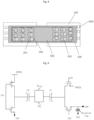
Fig. 1 is a structure diagram of an embodiment of a semiconductor structure according to the disclosure; -
Fig. 2 is an equivalent circuit diagram of an embodiment of the semiconductor structure inFig. 1 ; -
Fig. 3 is a structure diagram of an embodiment of a semiconductor structure according to the disclosure; -
Fig. 4 is a schematic diagram of an embodiment of a layout of a semiconductor structure according to the disclosure; -
Fig. 5 is a structure diagram of a charge pump including a semiconductor structure; -
Fig. 6 is a schematic layout diagram of a comparison embodiment of a semiconductor structure according to the disclosure; -
Fig. 7 is a structure diagram of a comparison embodiment of a semiconductor structure according to the disclosure; and -
Fig. 8 is an equivalent circuit diagram of an embodiment of the semiconductor structure inFig. 7 . - 10, first conductive layer; 20, capacitor bank; 21, capacitor; 30, capacitor plate; 31, first part; 32, second part; 33, third part; 40, first contact via; 50, second conductive layer; 60, second contact via; 100, first conductive layer pattern; 200, capacitor bank pattern; 201, capacitor pattern; 300, capacitor plate pattern; 400, first contact via pattern; 500, second conductive layer pattern; 600, second contact via pattern.
- It should be noted that the following detailed description is illustrative and is intended to provide a further description of the disclosure. Unless otherwise indicated, all technical and scientific terms used herein have the same meaning as that commonly understood by those of ordinary skill in the art to which the disclosure belongs.
- It is to be noted that terms used herein are only to describe specific embodiments, and are not intended to limit the exemplary embodiments of the disclosure. As used herein, unless otherwise explicitly indicated in the context, a singular form is also intended to include a plural form. In addition, it is also to be understood that when the terms "include" and/or "have" are used in the description, they are intended to indicate the presence of features, steps, operations, devices, components, and/or combinations thereof.
- It is to be understood that when a component (such as a layer, a film, an area, or a substrate) is described as being "on" another component, this component can be directly on the another component, or there can be an intermediate component. Further, in the specification and the claims, when a component is described as being "connected" to another component, this component can be "directly connected" to the another component or "connected" to the other component through a third component.
- As introduced in the background, in a semiconductor structure including a capacitor in the conventional art, the resistance of a capacitor plate on the capacitor is large, so the resistance of the semiconductor structure is large, which affects the performance of the semiconductor structure. In order to solve the above technical problem, the disclosure presents a semiconductor structure, a layout of the semiconductor structure and a semiconductor device.
- In a typical implementation mode of the disclosure, a semiconductor structure is provided. As shown in
Fig. 1 , the semiconductor structure includes a plurality of firstconductive layers 10 which are spaced, a plurality ofcapacitor banks 20, acapacitor plate 30 and a secondconductive layer 50. The plurality of thecapacitor banks 20 are on the plurality of firstconductive layers 10 in one-to-one correspondence. Thecapacitor bank 20 includes at least acapacitor 21. Eachcapacitor 21 includes a lower electrode layer, a capacitance dielectric layer and an upper electrode layer stacked from bottom to top, that is, the lower electrode layer is on the firstconductive layer 10, the capacitance dielectric layer is on the lower electrode layer, and the upper electrode layer is on the capacitance dielectric layer. The specific structure of thecapacitor bank 20 is not shown in the figure. Thecapacitor plate 30 is on each upper electrode layer, that is, the plurality of the capacitor banks are actually connected in series. The secondconductive layer 50 is above thecapacitor plate 30 and connected with thecapacitor plate 30. - In the above semiconductor structure, the second
conductive layer 50 is formed above thecapacitor plate 30, and the secondconductive layer 50 is connected with thecapacitor plate 30, so that in the semiconductor structure, the secondconductive layer 50 is equivalent to being connected in parallel at two ends of thecapacitor plate 30, that is, the secondconductive layer 50 is connected with thecapacitor plate 30 in parallel, and the resistance formed by the parallel connection of the second conductive layer and the capacitor plate is lower than the resistance of thecapacitor plate 30 itself. Therefore, compared to the semiconductor structure without the secondconductive layer 50, the resistance of the semiconductor structure with the secondconductive layer 50 is low, thereby avoiding the problem of affecting the performance due to the high resistance and improving the performance of the semiconductor structure. - As shown in
Fig. 1 , in a specific embodiment of the disclosure, the semiconductor structure further includes a first contact via 40, which is between thecapacitor plate 30 and the secondconductive layer 50, and is used for connecting thecapacitor plate 30 and the secondconductive layer 50. The secondconductive layer 50 and thecapacitor plate 30 can be more conveniently connected through the first contact via 40. The equivalent circuit diagram of the structure is shown inFig. 2 . It can be seen fromFig. 2 that the resistance of the part formed by thecapacitor plate 30, the secondconductive layer 50 and the first contact via 40 meets Rtotal=RCT+M1//RTCP, and RTCP is the resistance of thecapacitor plate 30, RCT+M1 is the resistance of the secondconductive layer 50 and the first contact via 40, and Rtotal is the equivalent resistance of thecapacitor plate 30 and the secondconductive layer 50 connected in parallel. Therefore, compared to the semiconductor structure without the secondconductive layer 50, the resistance in the structure is still low. - The materials of the first contact via in the disclosure are conductive materials, which can be selected according to the actual situation, including but not limited to wolfram (W), cuprum (Cu), nickel (Ni), aurum (Au) or argentum (Ag), etc.
- Specifically, the number of the first contact vias can be set according to the area of the second conductive layer, etc. There can be a plurality of the first contact vias, and there can also be one first contact via. For example, when the area of the second conductive layer is large, the number of the first contact vias can be set to be larger; when the area of the second conductive layer is small, the number of the first contact vias can be set to be small correspondingly. The larger the number of the first contact vias, the lower the overall equivalent resistance, and the lower the equivalent resistance of the
capacitor plate 30 and the secondconductive layer 50 connected in parallel. - In order to connect the second
conductive layer 50 and thecapacitor plate 30 better, and stably support the secondconductive layer 50, as shown inFig. 1 , in a specific embodiment of the disclosure, there are a plurality of thefirst contact vias 40, and the plurality of thefirst contact vias 40 are set intervals. - There can be one second
conductive layer 50, as shown inFig. 1 ; in this case, the area of the secondconductive layer 50 is approximately equal to that of the capacitor plate 30 (actually the area of the second conductive layer is slightly smaller). - Of course, there can be a plurality of the second
conductive layers 50. In an embodiment of the disclosure, as shown inFig. 3 , there are a plurality of the secondconductive layers 50, and the plurality of the secondconductive layers 50 are set intervals in a predetermined direction which is perpendicular to the thickness direction of the firstconductive layer 10. In this case, the sum of the areas of all of the plurality of the secondconductive layers 50 can be approximately equal to the area of thecapacitor plate 30. - It is also to be noted that when there is one second conductive layer, the second conductive layer can be formed by one or a plurality of metal materials. When the second conductive layer is formed by the plurality of the metal materials, the plurality of the metal materials can be mixed to form a single layer, or can form a metal layer separately, and the plurality of the metal materials form a plurality of the metal layers, and the plurality of the metal layers are superimposed to form the second conductive layer. When there are the plurality of the second conductive layers, the materials and thicknesses of the plurality of the second conductive layers can be the same or different. When the thicknesses are different, the height of the first contact via can also be adjusted. In addition, the specific material setting of each of the plurality of the second conductive layers can be seen in the case of one second conductive layer, which will not be described here.
- In another embodiment of the disclosure, the material of the first conductive layer of the disclosure can be metal, that is, the first conductive layer is a metal layer. The top of the first conductive layer is connected with the bottom of the lower electrode layer.
- The lower electrode layer of the disclosure can include conductive compounds formed by one or two of metal nitrides and metal silicides, such as Titanium Nitride, Titanium Silicide, Nickel Silicide, and TiSixNy. In a specific embodiment of the disclosure, the lower electrode layer includes a titanium nitride layer formed by Atomic Layer Deposition (ALD).
- The capacitance dielectric layer of the disclosure can be a high K dielectric layer, so as to improve the capacitance value per unit area, and can include a layer stack formed by nitrides or one of ZrOx, HfOx, ZrTiOx, RuOx, SbOx and AlOx or more than two of the group of the above materials.
- The upper electrode layer of the disclosure can include compounds formed by one or two of metal nitrides and metal silicides, such as Titanium Nitride, Titanium Silicide, Nickel Silicide, and TiSixNy. In a specific embodiment, the upper electrode layer include a titanium nitride layer formed by ALD.
- It is to be noted that the materials of the second conductive layer and the first conductive layer in the disclosure can include, but are not limited to, wolfram (W), cuprum (Cu), nickel (Ni), aurum (Au) or argentum (Ag), etc. The materials of the second conductive layer and the first conductive layer can be the same or different, and those skilled in the art can choose the suitable material according to the actual situation.
- The capacitor plate of the disclosure is a conductive layer, which can include conductive materials and semiconductor materials, such as Si and/or Ge. Suitable materials can be selected according to the actual situation to form the
capacitor plate 30 of the disclosure. - In a specific embodiment, as shown in
Fig. 1 , the semiconductor structure of the disclosure also includes a second contact via 60, which is on the firstconductive layer 10 and outside a predetermined area of the capacitor plate. The predetermined area is an area, in which the capacitor bank is set, of the first conductive layer. - The material of the second contact via is a conductive material, which can be selected according to the actual situation, including but not limited to wolfram (W), cuprum (Cu), nickel (Ni), aurum (Au) or argentum (Ag), etc.
- In a specific embodiment of the disclosure, there are a plurality of the
second contact vias 60. In the specific design process, one or more second contact vias can be set according to the actual situation, and the specific position can also be adjusted according to the actual situation. - In another typical implementation mode of the disclosure, a layout of a semiconductor structure is provided. As shown in
Fig. 4 , the layout includes a plurality of firstconductive layer patterns 100 which are set intervals, a plurality ofcapacitor bank patterns 200, acapacitor plate pattern 300 and a secondconductive layer pattern 500. Thecapacitor bank pattern 200 is on the firstconductive layer pattern 100 in one-to-one correspondence. Thecapacitor bank pattern 200 includes at least acapacitor pattern 201. Thecapacitor plate pattern 300 is overlaid on each of the plurality of thecapacitor bank patterns 200. The secondconductive layer pattern 500 is overlaid on at least a part of thecapacitor plate pattern 300. - In the layout of the semiconductor structure, the second conductive pattern is on the capacitor plate pattern, so that the second conductive layer is formed correspondingly on the capacitor plate in the semiconductor structure corresponding to the layout, that is, the second conductive layer connected with the capacitor plate is formed; the second conductive layer is equivalent to being connected in parallel at two ends of the capacitor plate, that is, the second conductive layer is connected with the capacitor plate in parallel, and the resistance formed by the parallel connection of the second conductive layer and the capacitor plate is lower than the resistance of the capacitor plate itself. Therefore, compared to the layout of the semiconductor structure without the second conductive layer pattern, the resistance of the semiconductor structure corresponding to the layout added the second conductive layer pattern is low, thereby avoiding the problem of affecting the performance due to the high resistance and improving the performance of the semiconductor structure.
- As shown in
Fig. 4 , in a specific embodiment of the disclosure, the semiconductor structure further includes a first contact viapattern 400, which is between thecapacitor plate pattern 300 and the secondconductive layer pattern 500. Specifically, the first contact viapattern 400 is on thecapacitor plate pattern 300, and the secondconductive layer pattern 500 is overlaid on the first contact viapattern 400. In this way, when the semiconductor structure corresponding to the layout is used, the corresponding first contact via pattern forms a first contact via, and the first contact via is connected with thecapacitor plate 30 and the secondconductive layer 50, as shown inFig. 1 . The secondconductive layer 50 and thecapacitor plate 30 can be more conveniently connected through the first contact via 40. The equivalent circuit diagram of the structure is shown inFig. 2 . It can be seen fromFig. 2 that the resistance of the part formed by thecapacitor plate 30, the secondconductive layer 50 and the first contact via 40 meets Rtotal=RCT+M1//RTCP, and RTCP is the resistance of thecapacitor plate 30, RCT+M1 is the resistance of the secondconductive layer 50 and the first contact via 40, and Rtotal is the equivalent resistance of thecapacitor plate 30 and the secondconductive layer 50 connected in parallel. Therefore, compared to the layout of the semiconductor structure without the secondconductive layer pattern 500, the layout makes the resistance in the corresponding semiconductor structure is still low. - It is to be noted that in order to display each pattern, so that those skilled in the art can more clearly know the position of each pattern,
Fig. 4 andFig. 6 of the disclosure are actually perspectives of the layout, that is, some patterns that have actually been covered by other patterns are also shown. InFig. 4 , thecapacitor bank pattern 200 that has been covered by thecapacitor plate pattern 300 is shown, and the first contact viapattern 400 that has been covered by the secondconductive layer pattern 500 is also shown. InFig. 6 , thecapacitor bank pattern 200 that has actually been covered by thecapacitor plate pattern 300 is shown. - Specifically, the number of the first contact via
patterns 400 can be set according to the area of the secondconductive layer pattern 500, etc. There can be a plurality of the first contact vias or one first contact via. For example, when the area of the secondconductive layer pattern 500 is large, the number of the first contact viapatterns 400 can be set to be larger; when the area of the secondconductive layer pattern 500 is small, the number of the first contact viapatterns 400 can be set to be smaller correspondingly. The larger the number of the first contact via patterns, the lower the overall equivalent resistance, and the lower the equivalent resistance of thecapacitor plate 30 and the secondconductive layer 50 connected in parallel. - In order to better connect the second
conductive layer 50 and thecapacitor plate 30 in the corresponding semiconductor structure, and stably support the secondconductive layer 50, as shown inFig. 4 , in a specific embodiment of the disclosure, there are a plurality of the first contact viapatterns 400, and the plurality of the first contact viapatterns 400 are spaced. - There can be one second
conductive layer pattern 500, as shown inFig. 4 ; in this case, the area of the secondconductive layer pattern 500 is approximately equal to that of the capacitor plate pattern 300 (the area of the second conductive layer pattern is slightly smaller). - Of course, there can be a plurality of the second
conductive layer patterns 500. In an embodiment of the disclosure, there are a plurality of the second conductive layer patterns, and the plurality of the second conductive layer patterns are spaced. In this case, the sum of the areas of all the second conductive layer patterns can be approximately equal to the area of thecapacitor plate pattern 300. - The capacitor in the semiconductor structure corresponding to the layout of the disclosure includes a lower electrode layer. The lower electrode layer can include conductive compounds formed by one or two of metal nitrides and metal silicides, such as Titanium Nitride, Titanium Silicide, Nickel Silicide, and TiSixNy. In a specific embodiment of the disclosure, the lower electrode layer can include a titanium nitride layer formed by ALD.
- The capacitor in the semiconductor structure corresponding to the layout of the disclosure includes a capacitance dielectric layer. The capacitance dielectric layer can be a high K dielectric layer, so as to improve the capacitance value per unit area, and can include a layer stack formed by nitrides or one of ZrOx, HfOx, ZrTiOx, RuOx, SbOx and AlOx or more than two of the group of the above materials. The capacitor in the semiconductor structure corresponding to the layout of the disclosure includes an upper electrode layer. The upper electrode layer can include compounds formed by one or two of metal nitrides and metal silicides, such as Titanium Nitride, Titanium Silicide, Nickel Silicide, and TiSixNy. In a specific embodiment, the upper electrode layer include a titanium nitride layer formed by ALD. It is also to be noted that the materials of the second conductive layer pattern and the first conductive layer in the semiconductor structure corresponding to the layout of the disclosure can include, but are not limited to, wolfram (W), cuprum (Cu), nickel (Ni), aurum (Au) or argentum (Ag), etc. The materials of the second conductive layer and the first conductive layer can be the same or different, and those skilled in the art can choose the suitable material according to the actual situation.
- The capacitor plate in the semiconductor structure corresponding to the layout of the disclosure is a conductive layer, which can include conductive materials and semiconductor materials, such as Si and/or Ge. Suitable materials can be selected according to the actual situation to form the capacitor plate of the disclosure.
- In a specific embodiment, as shown in
Fig. 4 , the layout of the disclosure also includes a second contact viapattern 600, which is on the firstconductive layer pattern 100 and outside a predetermined area of the capacitor plate pattern. The predetermined area is an area, in which thecapacitor bank pattern 200 is set, of the firstconductive layer pattern 100. Correspondingly, the material of the second contact via formed by the second contact via pattern is conductive material, which can be selected according to the actual situation, including but not limited to wolfram (W), cuprum (Cu), nickel (Ni), aurum (Au) or argentum (Ag), etc. In another embodiment of the disclosure, there are a plurality of the second contact viapatterns 600. - In another typical embodiment of the disclosure, a semiconductor device is also provided, which can include the above semiconductor structure; or a layout of the semiconductor device include any one of the above layout of the semiconductor structures. The above description can be referred to the specific semiconductor structure and the layout of the semiconductor structure, and elaborations are omitted herein.
- The above semiconductor device includes the above semiconductor structure. In the semiconductor structure, the second
conductive layer 50 is formed above thecapacitor plate 30, and the secondconductive layer 50 is connected with thecapacitor plate 30, so that in the semiconductor structure, the secondconductive layer 50 is equivalent to being connected in parallel at two ends of thecapacitor plate 30, that is, the secondconductive layer 50 is connected with thecapacitor plate 30 in parallel, and the resistance formed by the parallel connection of the second conductive layer and the capacitor plate is lower than the resistance of thecapacitor plate 30 itself. Therefore, compared to the semiconductor structure without the secondconductive layer 50, the resistance of the semiconductor structure with the secondconductive layer 50 is low, thereby avoiding the problem of affecting the performance due to the high resistance and improving the performance of the semiconductor device. - In a specific embodiment, the semiconductor device is a semiconductor memory. The semiconductor memory structure further includes a transistor structure. Each of a memory cell usually includes a
capacitor bank 20 and a transistor. A gate of the transistor is connected with a word line, a drain of the transistor is connected with a bit line, and a source of the transistor is connected with thecapacitor bank 20. A voltage signal of the word line can control the transistor on or off, and then data information stored in thecapacitor bank 20 is read through the bit line, or the data information is written to thecapacitor bank 20 through the bit line for storage. - In another embodiment of the disclosure, the above semiconductor device is a charge pump. The circuit diagram of the charge pump is shown in
Fig. 5 . The charge pump includes the above semiconductor structure, and for including the above semiconductor structure, its resistance is lower and less power is consumed, so that the pump efficiency of the charge pump is improved. - Of course, the semiconductor device of the disclosure is not limited to the semiconductor memory or the charge pump, but can also be any other device including the semiconductor structure, that is, those skilled in the art in the field can apply the semiconductor structure in any device needing it.
- In order to make those skilled in the art more clearly understand the technical solutions of the disclosure, elaborations will be given below in combination with specific embodiments.
- As shown in
Fig. 1 , the semiconductor structure is formed by a plurality of firstconductive layers 10, a plurality ofcapacitor banks 20, acapacitor plate 30, a plurality offirst contact vias 40 and a secondconductive layer 50. The plurality of firstconductive layers 10 are set intervals. A plurality of thecapacitor banks 20 are on the firstconductive layers 10 in one-to-one correspondence. Eachcapacitor 21 includes a lower electrode layer, a capacitance dielectric layer and an upper electrode layer stacked from bottom to top. Thecapacitor plate 30 is on each upper electrode layer. The secondconductive layer 50 is above thecapacitor plate 30 and connected with thecapacitor plate 30 through the plurality of thefirst contact vias 40. - The
capacitor plate 30 is formed by afirst part 31, asecond part 32 and athird part 33. The projection of thefirst part 31 on the firstconductive layers 10 is located on one of two adjacent firstconductive layers 10, the projection of thethird part 33 on the firstconductive layers 10 is located on the other of the two adjacent firstconductive layers 10, and thesecond part 32 is between thefirst part 31 and thesecond part 32. There are the plurality of thefirst contact vias 40 which are evenly distributed formed on thefirst part 31 and thethird part 33. - The second
conductive layer 50 is connected with each of the plurality of thefirst contact vias 40, and the projection of the secondconductive layer 50 on the firstconductive layers 10 can be located in the projection of thecapacitor plate 30 on the firstconductive layers 10. - The equivalent circuit structure of the structure shown in
Fig. 1 is shown inFig. 2 , correspondingly, the equivalent resistance of the part inFig. 1 meets Rtotal1=RCT+M1//RTCP, and RCT+M1 is the resistance value of the secondconductive layer 50 and the first contact via 40 connected in series, and RTCP is the resistance of thecapacitor plate 30. - Unlike the embodiment, the semiconductor structure does not include the second
conductive layer 50 and the first contact via 40. Its layout is shown inFig. 6 , its structure is shown inFig. 7 , and its equivalent circuit structure is shown inFig. 8 . The equivalent resistance of the part inFig. 7 meets Rtotal2=RTCP, and RTCP is the resistance of thecapacitor plate 30. - It can be known from the comparison of the equivalent resistance in the above embodiment and comparison embodiment, the resistance of the semiconductor structure is reduced due to adding the first contact via 40 and the second
conductive layer 50 in the embodiment. - It can be seen from above description that the above embodiments of the disclosure achieve the following technical effects.
- 1) In the semiconductor structure of the disclosure, the second conductive layer is formed above the capacitor plate, and the second conductive layer is connected with the capacitor plate, so that in the semiconductor structure, the second conductive layer is equivalent to being connected in parallel at two ends of the capacitor plate, that is, the second conductive layer is connected with the capacitor plate in parallel, and the resistance formed by the parallel connection of the second conductive layer and the capacitor plate is lower than the resistance of the capacitor plate itself. Therefore, compared to the semiconductor structure without the second conductive layer, the resistance of the semiconductor structure with the second conductive layer is low, thereby avoiding the problem of affecting the performance due to the high resistance and improving the performance of the semiconductor structure.
- 2) The semiconductor device of the disclosure includes the semiconductor structure. In the semiconductor structure, the second conductive layer is formed above the capacitor plate, and the second conductive layer is connected with the capacitor plate, so that in the semiconductor structure, the second conductive layer is equivalent to being connected in parallel at two ends of the capacitor plate, that is, the second conductive layer is connected with the capacitor plate in parallel, and the resistance formed by the parallel connection of the second conductive layer and the capacitor plate is lower than the resistance of the capacitor plate itself. Therefore, compared to the semiconductor structure without the second conductive layer, the resistance of the semiconductor structure with the second conductive layer is low, thereby avoiding the problem of affecting the performance due to the high resistance and improving the performance of the semiconductor device.
- 3) In the layout of the semiconductor structure of the disclosure, the second conductive pattern is on the capacitor plate pattern, so that the second conductive layer is formed correspondingly on the capacitor plate in the semiconductor structure corresponding to the layout, that is, the second conductive layer connected with the capacitor plate is formed; the second conductive layer is equivalent to being connected in parallel at two ends of the capacitor plate, that is, the second conductive layer is connected with the capacitor plate in parallel, and the resistance formed by the parallel connection of the second conductive layer and the capacitor plate is lower than the resistance of the capacitor plate itself. Therefore, compared to the layout of the semiconductor structure without the second conductive layer pattern, the resistance of the semiconductor structure corresponding to the layout added the second conductive layer pattern is low, thereby avoiding the problem of affecting the performance due to the high resistance and improving the performance of the semiconductor structure.
- The above is only the preferred embodiments of the disclosure and not intended to limit the disclosure; for those skilled in the art, the disclosure can have various modifications and changes. Any modifications, equivalent replacements, improvements and the like within the spirit and principle of the disclosure should fall within the protection scope of the claims of the disclosure.
Claims (15)
- A semiconductor structure, comprising:a plurality of first conductive layers that are spaced;a plurality of capacitor banks, and the capacitor bank being on the first conductive layer in one-to-one correspondence and the capacitor bank comprising at least a capacitor, each capacitor comprising a lower electrode layer, a capacitance dielectric layer and an upper electrode layer stacked from bottom to top;a capacitor plate, wherein the capacitor plate is on each upper electrode layer; anda second conductive layer, wherein the second conductive layer is above the capacitor plate and connected with the capacitor plate.
- The semiconductor structure according to claim 1, the semiconductor structure further comprises:
a first contact via, wherein the first contact via is between the capacitor plate and the second conductive layer, and is configured to connect the capacitor plate and the second conductive layer. - The semiconductor structure according to claim 2, wherein there are a plurality of the first contact vias, and the plurality of the first contact vias are set intervals.
- The semiconductor structure according to claim 1, wherein each of the plurality of the capacitor banks comprises a plurality of capacitors.
- The semiconductor structure according to claim 1, the semiconductor structure further comprises:
a second contact via, wherein the second contact via is on the first conductive layer and outside a predetermined area, the predetermined area being an area, in which the capacitor bank is set, of the first conductive layer. - The semiconductor structure according to claim 5, wherein there are a plurality of the second contact vias.
- The semiconductor structure according to claim 5, wherein the first conductive layer and the second conductive layer are metal layer, or the first conductive layer or the second conductive layer is the metal layer.
- A layout of a semiconductor structure, comprising:a plurality of first conductive layer patterns that are set intervals;a plurality of capacitor bank patterns, and the capacitor bank pattern being on the first conductive layer pattern in one-to-one correspondence, the capacitor bank pattern comprising at least a capacitor pattern;a capacitor plate pattern, wherein the capacitor plate pattern is overlaid on each of the plurality of the capacitor bank patterns; anda second conductive layer pattern, wherein the second conductive layer pattern is overlaid on at least a part of the capacitor plate pattern.
- The layout according to claim 8, the layout further comprises:a first contact via pattern, wherein the first contact via pattern is on the capacitor plate pattern;the second conductive layer pattern overlays on the first contact via pattern.
- The layout according to claim 9, wherein there are a plurality of the first contact via patterns that are set intervals, and the second conductive layer pattern is overlaid on all of the plurality of the first contact via patterns.
- The layout according to claim 8, the layout further comprises:
a second contact via pattern, wherein the second contact via pattern is on the first conductive layer pattern and outside a predetermined area, the predetermined area being an area, in which the capacitor bank pattern is set, of the first conductive layer pattern. - The layout according to claim 11, wherein there are a plurality of the second contact via patterns.
- The layout according to claim 8, wherein the capacitor bank pattern comprises a plurality of the capacitor patterns.
- A semiconductor device, comprising the semiconductor structure according to any one of claims 1 to 7, or a layout of the semiconductor device comprises the layout of the semiconductor structure according to any one of claims 8 to 13.
- The semiconductor device according to claim 14, wherein the semiconductor device is a semiconductor memory.
Applications Claiming Priority (2)
| Application Number | Priority Date | Filing Date | Title |
|---|---|---|---|
| CN202110915940.3A CN115706110A (en) | 2021-08-10 | 2021-08-10 | Semiconductor structure, layout thereof and semiconductor device |
| PCT/CN2021/119422 WO2023015678A1 (en) | 2021-08-10 | 2021-09-18 | Semiconductor structure and layout thereof, and semiconductor device |
Publications (2)
| Publication Number | Publication Date |
|---|---|
| EP4156187A1 true EP4156187A1 (en) | 2023-03-29 |
| EP4156187A4 EP4156187A4 (en) | 2023-11-01 |
Family
ID=85176437
Family Applications (1)
| Application Number | Title | Priority Date | Filing Date |
|---|---|---|---|
| EP21916637.8A Withdrawn EP4156187A4 (en) | 2021-08-10 | 2021-09-18 | SEMICONDUCTOR STRUCTURE AND ITS ARRANGEMENT, AND SEMICONDUCTOR DEVICE |
Country Status (4)
| Country | Link |
|---|---|
| US (1) | US20230050145A1 (en) |
| EP (1) | EP4156187A4 (en) |
| JP (1) | JP2023540594A (en) |
| KR (1) | KR20230047178A (en) |
Family Cites Families (7)
| Publication number | Priority date | Publication date | Assignee | Title |
|---|---|---|---|---|
| JP3045419B2 (en) * | 1991-11-08 | 2000-05-29 | ローム株式会社 | Dielectric film capacitors |
| JP3900542B2 (en) * | 1997-03-24 | 2007-04-04 | セイコーエプソン株式会社 | Semiconductor capacitance device and semiconductor device using the same |
| US7282757B2 (en) * | 2003-10-20 | 2007-10-16 | Taiwan Semiconductor Manufacturing Company, Ltd. | MIM capacitor structure and method of manufacture |
| JP2005136074A (en) * | 2003-10-29 | 2005-05-26 | Kyocera Corp | Capacitor, series capacitor and variable capacitor |
| US9666262B2 (en) * | 2012-03-13 | 2017-05-30 | Samsung Electronics Co., Ltd. | Semiconductor memory device including power decoupling capacitor |
| KR20160035407A (en) * | 2014-09-23 | 2016-03-31 | 삼성전자주식회사 | Semiconductor devices and methods of manufacturing the same |
| KR20190140162A (en) * | 2018-06-11 | 2019-12-19 | 삼성전자주식회사 | Semiconductor memory device, power decoupling capacitor array thereof, and memory system having the same |
-
2021
- 2021-09-18 KR KR1020237008302A patent/KR20230047178A/en not_active Ceased
- 2021-09-18 JP JP2023515371A patent/JP2023540594A/en active Pending
- 2021-09-18 EP EP21916637.8A patent/EP4156187A4/en not_active Withdrawn
-
2022
- 2022-04-28 US US17/661,085 patent/US20230050145A1/en not_active Abandoned
Also Published As
| Publication number | Publication date |
|---|---|
| EP4156187A4 (en) | 2023-11-01 |
| KR20230047178A (en) | 2023-04-06 |
| JP2023540594A (en) | 2023-09-25 |
| US20230050145A1 (en) | 2023-02-16 |
Similar Documents
| Publication | Publication Date | Title |
|---|---|---|
| US12113052B2 (en) | Memory devices and electronic systems | |
| US20240381626A1 (en) | Memory, method for manufacturing memory, and electronic device | |
| CN116209258B (en) | Storage structure and preparation method of storage unit | |
| TWI894044B (en) | Microelectronic devices and methods of forming microelectronic devices | |
| KR20190024251A (en) | Semiconductor device | |
| US20030013210A1 (en) | Ferroelectric circuit element that can be fabricated at low temperatures and method for making the same | |
| EP4380330A1 (en) | Memory cell, 3d memory and preparation method therefor, and electronic device | |
| US20150364474A1 (en) | Semiconductor devices and methods of manufacturing the same | |
| WO2025213726A1 (en) | Semiconductor device and manufacturing method therefor, and electronic device | |
| US11672128B2 (en) | Methods of incorporating leaker devices into capacitor configurations to reduce cell disturb, and capacitor configurations incorporating leaker devices | |
| US20260018561A1 (en) | Microelectronic devices, and related methods and electronic systems | |
| US20230050145A1 (en) | Semiconductor Structure, Layout of Semiconductor Structure and Semiconductor Device | |
| TWI825814B (en) | Semiconductor structures, their layouts, and semiconductor devices | |
| TWI827230B (en) | Semiconductor structure and manufacturing method thereof, memory chip, electronic device | |
| US20240244820A1 (en) | Microelectronic devices, and related memory devices, and electronic systems | |
| US20230413508A1 (en) | Semiconductor structure and method for manufacturing semiconductor structure | |
| CN115843181B (en) | Memory device and manufacturing method thereof | |
| WO2022086609A1 (en) | Widened conductive line structures and staircase structures for semiconductor devices | |
| US6084261A (en) | DRAM cell with a fork-shaped capacitor | |
| JP4602635B2 (en) | Semiconductor device | |
| KR20030002202A (en) | Method for fabricating a merged semiconductor memory device | |
| US20250240940A1 (en) | Semiconductor device and manufacturing method thereof | |
| US20250048629A1 (en) | Semiconductor device and manufacturing method of the semiconductor device | |
| US20260107440A1 (en) | Semiconductor device | |
| KR20250090571A (en) | Semiconductor Device Including a Selector and a Buffer Layer |
Legal Events
| Date | Code | Title | Description |
|---|---|---|---|
| STAA | Information on the status of an ep patent application or granted ep patent |
Free format text: STATUS: UNKNOWN |
|
| STAA | Information on the status of an ep patent application or granted ep patent |
Free format text: STATUS: THE INTERNATIONAL PUBLICATION HAS BEEN MADE |
|
| PUAI | Public reference made under article 153(3) epc to a published international application that has entered the european phase |
Free format text: ORIGINAL CODE: 0009012 |
|
| STAA | Information on the status of an ep patent application or granted ep patent |
Free format text: STATUS: REQUEST FOR EXAMINATION WAS MADE |
|
| 17P | Request for examination filed |
Effective date: 20220712 |
|
| AK | Designated contracting states |
Kind code of ref document: A1 Designated state(s): AL AT BE BG CH CY CZ DE DK EE ES FI FR GB GR HR HU IE IS IT LI LT LU LV MC MK MT NL NO PL PT RO RS SE SI SK SM TR |
|
| REG | Reference to a national code |
Ref country code: DE Ref legal event code: R079 Free format text: PREVIOUS MAIN CLASS: G11C0011406300 Ipc: G11C0005060000 |
|
| A4 | Supplementary search report drawn up and despatched |
Effective date: 20231005 |
|
| RIC1 | Information provided on ipc code assigned before grant |
Ipc: H01L 27/01 20060101ALN20230928BHEP Ipc: G11C 11/4074 20060101ALN20230928BHEP Ipc: G11C 11/401 20060101ALN20230928BHEP Ipc: G11C 11/22 20060101ALN20230928BHEP Ipc: G11C 5/14 20060101ALN20230928BHEP Ipc: G11C 5/02 20060101ALN20230928BHEP Ipc: G11C 5/10 20060101ALI20230928BHEP Ipc: G11C 5/06 20060101AFI20230928BHEP |
|
| STAA | Information on the status of an ep patent application or granted ep patent |
Free format text: STATUS: THE APPLICATION HAS BEEN WITHDRAWN |
|
| 18W | Application withdrawn |
Effective date: 20231208 |