EP4152381A1 - An integrated circuit chip comprising back-side power delivery tracks - Google Patents
An integrated circuit chip comprising back-side power delivery tracks Download PDFInfo
- Publication number
- EP4152381A1 EP4152381A1 EP21197018.1A EP21197018A EP4152381A1 EP 4152381 A1 EP4152381 A1 EP 4152381A1 EP 21197018 A EP21197018 A EP 21197018A EP 4152381 A1 EP4152381 A1 EP 4152381A1
- Authority
- EP
- European Patent Office
- Prior art keywords
- tsvs
- power delivery
- power
- power rails
- rails
- Prior art date
- Legal status (The legal status is an assumption and is not a legal conclusion. Google has not performed a legal analysis and makes no representation as to the accuracy of the status listed.)
- Granted
Links
Images





Classifications
-
- H—ELECTRICITY
- H10—SEMICONDUCTOR DEVICES; ELECTRIC SOLID-STATE DEVICES NOT OTHERWISE PROVIDED FOR
- H10W—GENERIC PACKAGES, INTERCONNECTIONS, CONNECTORS OR OTHER CONSTRUCTIONAL DETAILS OF DEVICES COVERED BY CLASS H10
- H10W20/00—Interconnections in chips, wafers or substrates
- H10W20/40—Interconnections external to wafers or substrates, e.g. back-end-of-line [BEOL] metallisations or vias connecting to gate electrodes
- H10W20/41—Interconnections external to wafers or substrates, e.g. back-end-of-line [BEOL] metallisations or vias connecting to gate electrodes characterised by their conductive parts
- H10W20/427—Power or ground buses
-
- H—ELECTRICITY
- H10—SEMICONDUCTOR DEVICES; ELECTRIC SOLID-STATE DEVICES NOT OTHERWISE PROVIDED FOR
- H10D—INORGANIC ELECTRIC SEMICONDUCTOR DEVICES
- H10D89/00—Aspects of integrated devices not covered by groups H10D84/00 - H10D88/00
- H10D89/10—Integrated device layouts
-
- H—ELECTRICITY
- H10—SEMICONDUCTOR DEVICES; ELECTRIC SOLID-STATE DEVICES NOT OTHERWISE PROVIDED FOR
- H10W—GENERIC PACKAGES, INTERCONNECTIONS, CONNECTORS OR OTHER CONSTRUCTIONAL DETAILS OF DEVICES COVERED BY CLASS H10
- H10W20/00—Interconnections in chips, wafers or substrates
- H10W20/01—Manufacture or treatment
- H10W20/021—Manufacture or treatment of interconnections within wafers or substrates
-
- H—ELECTRICITY
- H10—SEMICONDUCTOR DEVICES; ELECTRIC SOLID-STATE DEVICES NOT OTHERWISE PROVIDED FOR
- H10W—GENERIC PACKAGES, INTERCONNECTIONS, CONNECTORS OR OTHER CONSTRUCTIONAL DETAILS OF DEVICES COVERED BY CLASS H10
- H10W20/00—Interconnections in chips, wafers or substrates
- H10W20/01—Manufacture or treatment
- H10W20/021—Manufacture or treatment of interconnections within wafers or substrates
- H10W20/023—Manufacture or treatment of interconnections within wafers or substrates the interconnections being through-semiconductor vias
-
- H—ELECTRICITY
- H10—SEMICONDUCTOR DEVICES; ELECTRIC SOLID-STATE DEVICES NOT OTHERWISE PROVIDED FOR
- H10W—GENERIC PACKAGES, INTERCONNECTIONS, CONNECTORS OR OTHER CONSTRUCTIONAL DETAILS OF DEVICES COVERED BY CLASS H10
- H10W20/00—Interconnections in chips, wafers or substrates
- H10W20/01—Manufacture or treatment
- H10W20/021—Manufacture or treatment of interconnections within wafers or substrates
- H10W20/023—Manufacture or treatment of interconnections within wafers or substrates the interconnections being through-semiconductor vias
- H10W20/0245—Manufacture or treatment of interconnections within wafers or substrates the interconnections being through-semiconductor vias comprising use of blind vias during the manufacture
-
- H—ELECTRICITY
- H10—SEMICONDUCTOR DEVICES; ELECTRIC SOLID-STATE DEVICES NOT OTHERWISE PROVIDED FOR
- H10W—GENERIC PACKAGES, INTERCONNECTIONS, CONNECTORS OR OTHER CONSTRUCTIONAL DETAILS OF DEVICES COVERED BY CLASS H10
- H10W20/00—Interconnections in chips, wafers or substrates
- H10W20/01—Manufacture or treatment
- H10W20/021—Manufacture or treatment of interconnections within wafers or substrates
- H10W20/023—Manufacture or treatment of interconnections within wafers or substrates the interconnections being through-semiconductor vias
- H10W20/0249—Manufacture or treatment of interconnections within wafers or substrates the interconnections being through-semiconductor vias wherein the through-semiconductor via protrudes from backsides of the chips, wafers or substrates during the manufacture
-
- H—ELECTRICITY
- H10—SEMICONDUCTOR DEVICES; ELECTRIC SOLID-STATE DEVICES NOT OTHERWISE PROVIDED FOR
- H10W—GENERIC PACKAGES, INTERCONNECTIONS, CONNECTORS OR OTHER CONSTRUCTIONAL DETAILS OF DEVICES COVERED BY CLASS H10
- H10W20/00—Interconnections in chips, wafers or substrates
- H10W20/20—Interconnections within wafers or substrates, e.g. through-silicon vias [TSV]
-
- H—ELECTRICITY
- H10—SEMICONDUCTOR DEVICES; ELECTRIC SOLID-STATE DEVICES NOT OTHERWISE PROVIDED FOR
- H10W—GENERIC PACKAGES, INTERCONNECTIONS, CONNECTORS OR OTHER CONSTRUCTIONAL DETAILS OF DEVICES COVERED BY CLASS H10
- H10W20/00—Interconnections in chips, wafers or substrates
- H10W20/20—Interconnections within wafers or substrates, e.g. through-silicon vias [TSV]
- H10W20/211—Through-semiconductor vias, e.g. TSVs
- H10W20/212—Top-view shapes or dispositions, e.g. top-view layouts of the vias
-
- H—ELECTRICITY
- H10—SEMICONDUCTOR DEVICES; ELECTRIC SOLID-STATE DEVICES NOT OTHERWISE PROVIDED FOR
- H10W—GENERIC PACKAGES, INTERCONNECTIONS, CONNECTORS OR OTHER CONSTRUCTIONAL DETAILS OF DEVICES COVERED BY CLASS H10
- H10W20/00—Interconnections in chips, wafers or substrates
- H10W20/20—Interconnections within wafers or substrates, e.g. through-silicon vias [TSV]
- H10W20/211—Through-semiconductor vias, e.g. TSVs
- H10W20/212—Top-view shapes or dispositions, e.g. top-view layouts of the vias
- H10W20/2125—Top-view shapes
-
- H—ELECTRICITY
- H10—SEMICONDUCTOR DEVICES; ELECTRIC SOLID-STATE DEVICES NOT OTHERWISE PROVIDED FOR
- H10W—GENERIC PACKAGES, INTERCONNECTIONS, CONNECTORS OR OTHER CONSTRUCTIONAL DETAILS OF DEVICES COVERED BY CLASS H10
- H10W20/00—Interconnections in chips, wafers or substrates
- H10W20/20—Interconnections within wafers or substrates, e.g. through-silicon vias [TSV]
- H10W20/211—Through-semiconductor vias, e.g. TSVs
- H10W20/218—Through-semiconductor vias, e.g. TSVs in silicon-on-insulator [SOI] wafers
-
- H—ELECTRICITY
- H10—SEMICONDUCTOR DEVICES; ELECTRIC SOLID-STATE DEVICES NOT OTHERWISE PROVIDED FOR
- H10W—GENERIC PACKAGES, INTERCONNECTIONS, CONNECTORS OR OTHER CONSTRUCTIONAL DETAILS OF DEVICES COVERED BY CLASS H10
- H10W20/00—Interconnections in chips, wafers or substrates
- H10W20/40—Interconnections external to wafers or substrates, e.g. back-end-of-line [BEOL] metallisations or vias connecting to gate electrodes
- H10W20/41—Interconnections external to wafers or substrates, e.g. back-end-of-line [BEOL] metallisations or vias connecting to gate electrodes characterised by their conductive parts
- H10W20/42—Vias, e.g. via plugs
-
- H—ELECTRICITY
- H10—SEMICONDUCTOR DEVICES; ELECTRIC SOLID-STATE DEVICES NOT OTHERWISE PROVIDED FOR
- H10W—GENERIC PACKAGES, INTERCONNECTIONS, CONNECTORS OR OTHER CONSTRUCTIONAL DETAILS OF DEVICES COVERED BY CLASS H10
- H10W20/00—Interconnections in chips, wafers or substrates
- H10W20/40—Interconnections external to wafers or substrates, e.g. back-end-of-line [BEOL] metallisations or vias connecting to gate electrodes
- H10W20/41—Interconnections external to wafers or substrates, e.g. back-end-of-line [BEOL] metallisations or vias connecting to gate electrodes characterised by their conductive parts
- H10W20/43—Layouts of interconnections
-
- H—ELECTRICITY
- H10—SEMICONDUCTOR DEVICES; ELECTRIC SOLID-STATE DEVICES NOT OTHERWISE PROVIDED FOR
- H10W—GENERIC PACKAGES, INTERCONNECTIONS, CONNECTORS OR OTHER CONSTRUCTIONAL DETAILS OF DEVICES COVERED BY CLASS H10
- H10W20/00—Interconnections in chips, wafers or substrates
- H10W20/40—Interconnections external to wafers or substrates, e.g. back-end-of-line [BEOL] metallisations or vias connecting to gate electrodes
- H10W20/481—Interconnections external to wafers or substrates, e.g. back-end-of-line [BEOL] metallisations or vias connecting to gate electrodes on the rear surfaces of the wafers or substrates
-
- H—ELECTRICITY
- H10—SEMICONDUCTOR DEVICES; ELECTRIC SOLID-STATE DEVICES NOT OTHERWISE PROVIDED FOR
- H10D—INORGANIC ELECTRIC SEMICONDUCTOR DEVICES
- H10D84/00—Integrated devices formed in or on semiconductor substrates that comprise only semiconducting layers, e.g. on Si wafers or on GaAs-on-Si wafers
- H10D84/01—Manufacture or treatment
- H10D84/0123—Integrating together multiple components covered by H10D12/00 or H10D30/00, e.g. integrating multiple IGBTs
- H10D84/0126—Integrating together multiple components covered by H10D12/00 or H10D30/00, e.g. integrating multiple IGBTs the components including insulated gates, e.g. IGFETs
- H10D84/0165—Integrating together multiple components covered by H10D12/00 or H10D30/00, e.g. integrating multiple IGBTs the components including insulated gates, e.g. IGFETs the components including complementary IGFETs, e.g. CMOS devices
- H10D84/0193—Integrating together multiple components covered by H10D12/00 or H10D30/00, e.g. integrating multiple IGBTs the components including insulated gates, e.g. IGFETs the components including complementary IGFETs, e.g. CMOS devices the components including FinFETs
-
- H—ELECTRICITY
- H10—SEMICONDUCTOR DEVICES; ELECTRIC SOLID-STATE DEVICES NOT OTHERWISE PROVIDED FOR
- H10D—INORGANIC ELECTRIC SEMICONDUCTOR DEVICES
- H10D84/00—Integrated devices formed in or on semiconductor substrates that comprise only semiconducting layers, e.g. on Si wafers or on GaAs-on-Si wafers
- H10D84/01—Manufacture or treatment
- H10D84/02—Manufacture or treatment characterised by using material-based technologies
- H10D84/03—Manufacture or treatment characterised by using material-based technologies using Group IV technology, e.g. silicon technology or silicon-carbide [SiC] technology
- H10D84/038—Manufacture or treatment characterised by using material-based technologies using Group IV technology, e.g. silicon technology or silicon-carbide [SiC] technology using silicon technology, e.g. SiGe
-
- H—ELECTRICITY
- H10—SEMICONDUCTOR DEVICES; ELECTRIC SOLID-STATE DEVICES NOT OTHERWISE PROVIDED FOR
- H10D—INORGANIC ELECTRIC SEMICONDUCTOR DEVICES
- H10D84/00—Integrated devices formed in or on semiconductor substrates that comprise only semiconducting layers, e.g. on Si wafers or on GaAs-on-Si wafers
- H10D84/80—Integrated devices formed in or on semiconductor substrates that comprise only semiconducting layers, e.g. on Si wafers or on GaAs-on-Si wafers characterised by the integration of at least one component covered by groups H10D12/00 or H10D30/00, e.g. integration of IGFETs
- H10D84/82—Integrated devices formed in or on semiconductor substrates that comprise only semiconducting layers, e.g. on Si wafers or on GaAs-on-Si wafers characterised by the integration of at least one component covered by groups H10D12/00 or H10D30/00, e.g. integration of IGFETs of only field-effect components
- H10D84/83—Integrated devices formed in or on semiconductor substrates that comprise only semiconducting layers, e.g. on Si wafers or on GaAs-on-Si wafers characterised by the integration of at least one component covered by groups H10D12/00 or H10D30/00, e.g. integration of IGFETs of only field-effect components of only insulated-gate FETs [IGFET]
- H10D84/85—Complementary IGFETs, e.g. CMOS
- H10D84/853—Complementary IGFETs, e.g. CMOS comprising FinFETs
-
- H—ELECTRICITY
- H10—SEMICONDUCTOR DEVICES; ELECTRIC SOLID-STATE DEVICES NOT OTHERWISE PROVIDED FOR
- H10D—INORGANIC ELECTRIC SEMICONDUCTOR DEVICES
- H10D84/00—Integrated devices formed in or on semiconductor substrates that comprise only semiconducting layers, e.g. on Si wafers or on GaAs-on-Si wafers
- H10D84/90—Masterslice integrated circuits
- H10D84/903—Masterslice integrated circuits comprising field effect technology
- H10D84/907—CMOS gate arrays
- H10D84/968—Macro-architecture
- H10D84/974—Layout specifications, i.e. inner core regions
- H10D84/981—Power supply lines
-
- H—ELECTRICITY
- H10—SEMICONDUCTOR DEVICES; ELECTRIC SOLID-STATE DEVICES NOT OTHERWISE PROVIDED FOR
- H10D—INORGANIC ELECTRIC SEMICONDUCTOR DEVICES
- H10D86/00—Integrated devices formed in or on insulating or conducting substrates, e.g. formed in silicon-on-insulator [SOI] substrates or on stainless steel or glass substrates
- H10D86/01—Manufacture or treatment
- H10D86/011—Manufacture or treatment comprising FinFETs
-
- H—ELECTRICITY
- H10—SEMICONDUCTOR DEVICES; ELECTRIC SOLID-STATE DEVICES NOT OTHERWISE PROVIDED FOR
- H10D—INORGANIC ELECTRIC SEMICONDUCTOR DEVICES
- H10D86/00—Integrated devices formed in or on insulating or conducting substrates, e.g. formed in silicon-on-insulator [SOI] substrates or on stainless steel or glass substrates
- H10D86/201—Integrated devices formed in or on insulating or conducting substrates, e.g. formed in silicon-on-insulator [SOI] substrates or on stainless steel or glass substrates the substrates comprising an insulating layer on a semiconductor body, e.g. SOI
- H10D86/215—Integrated devices formed in or on insulating or conducting substrates, e.g. formed in silicon-on-insulator [SOI] substrates or on stainless steel or glass substrates the substrates comprising an insulating layer on a semiconductor body, e.g. SOI comprising FinFETs
-
- H—ELECTRICITY
- H10—SEMICONDUCTOR DEVICES; ELECTRIC SOLID-STATE DEVICES NOT OTHERWISE PROVIDED FOR
- H10W—GENERIC PACKAGES, INTERCONNECTIONS, CONNECTORS OR OTHER CONSTRUCTIONAL DETAILS OF DEVICES COVERED BY CLASS H10
- H10W46/00—Marks applied to devices, e.g. for alignment or identification
Definitions
- the present invention is related to integrated circuit chips, hereafter abbreviated to ICs or IC chips, in particular to the aspect of the delivery of power to the active devices on the chip.
- CMOS devices In advanced CMOS devices, electronic circuits are designed and realized as combinations of so-called standard cells : combinations of n- and p-MOS devices organized in rectangular cells bound on two sides by respectively a supply and a reference (usually ground) power supply track, coupled to voltages which are usually labelled Vdd and Vss respectively.
- These power supply tracks are traditionally connected to metal traces higher in the back end of line metal stack, collecting all the currents from the small pitches at transistor level to the large pitches at power and ground level.
- the resistance of the metal tracks at the standard cell level have become a bottleneck for the power supply, resulting in large voltage drops of the supply current and reducing overall potential device performance.
- buried power rails Basically, the tracks used for Vdd and Vss that are typically horizontal (broad & thin) are now realized vertically (narrow/heigh) and recessed ("buried") between the fins or nano-sheets onto which the active devices in advance CMOS standard cells are built.
- the TSVs have to be realized without contacting adjacent power rails, setting a limit to the width of these TSVs that takes into account the minimal spacing to the neighbouring Vdd or Vss track and the expected overlay tolerance when patterning the TSVs from the wafer backside.
- the TSV width needs to exceed the width of the power rails.
- the area where the TSV is landing on the Vdd and Vss rails cannot be used for placement of regular standard cells.
- the TSVs are elongate slit-shaped TSVs aligned to the power rails and arranged in a staggered pattern, so that any one of the power delivery tracks is connected to a first row of mutually parallel TSVs, and the power delivery track or tracks directly adjacent to said power delivery track is connected to another row of TSVs which are staggered relative to the TSVs of the first row.
- the staggered arrangement of the TSVs enables a more relaxed overlay tolerance in the patterning steps required to form the power delivery tracks on the back side, while still allowing a very dense interconnectivity of the TSVs, thereby also ensuring that a low resistive path is formed from the power supply to the active devices at the front of the substrate.
- the distance between two directly adjacent TSVs which are mutually aligned along their longitudinal direction is smaller than or equal to the length of the TSVs.
- the width of the power delivery tracks is essentially equal to the distance between directly adjacent power delivery tracks.
- the power rails are buried only in said dielectric layer and not in the substrate.
- the active devices are fin-based devices or nano-sheet based devices and wherein the power rails run parallel to the fins or to the nano-sheets.
- the power delivery tracks are essentially perpendicular to the buried power rails.
- the invention is also related to a method for producing an IC chip according to the invention, the method comprising the steps of :
- the power delivery tracks are essentially perpendicular to the power rails.
- an embodiment of an integrated circuit chip according to the invention is described.
- the IC chip is produced by processing a CMOS layout of finFET transistors arranged in standard cells on a semiconductor device wafer.
- the invention is not limited to this particular application field.
- the invention is related also to a specific method for producing the chip according to the invention, this method is described first on a step-by-step basis, with reference to Figures 1a to 1l .
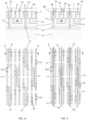
- Figure 1a shows a small portion of a device wafer, comprising a monocrystalline Si layer 1, into which a number of fins 2 and 2' have been produced by a known lithography and etch technique, applying etch masks 3.
- the width of the fins may be in the order of 10 nm or less.
- the two different types of hatching indicate different doping types (referred to also by respective references 2 and 2'), typically p-type and n-type doping.
- the Si layer 1 is a p-type layer, implanted with n-type dopants in consecutive well-areas 4.
- the well-areas 4 reach about half the depth of the Si layer 1 but could also reach to the back surface of the Si layer.
- the image is merely a schematic indication of the fact that adjacent p- and n-areas are created on the device wafer.
- This layout is typically used for producing pMOS and nMOS transistors arranged in multiple standard cells.
- alternate pairs of 2 p-type fins 2 and 2 n-type fins 2' are arranged with equal distances between the fins.
- the fin lengths differ and that the fins are arranged according to a pattern.
- the pattern shown is a random example of a possible fin pattern.
- the Si layer 1 is a monocrystalline top layer of a multi-layer device wafer comprising a base wafer 5, typically a Si wafer, and a thin etch stop layer 6, which could be a SiGe layer.
- the Si layer 1 (including the fins) preferably has a thickness less than 1 ⁇ m, for example about 500 nm.
- the etch stop layer 6 may be a SiGe layer of about 50nm thick for example. Its function as an etch stop layer is to stop the etching of the base wafer 5 for the removal of said base wafer from the back side, as will be explained later in this description.
- the SiGe layer 6 and the monocrystalline Si layer 1 may be produced on a Si base wafer 5 by techniques well known in the art, preferably by epitaxial growth methods.
- SOI silicon-on-insulator
- the fins 2, 2' are embedded in a layer 7 of dielectric material. Typically, this is a layer of silicon oxide (SiO 2 ), also referred to as 'shallow trench isolation' oxide. We will hereafter refer to this layer as the STI layer 7.
- a plurality of slits 10 is produced through the STI layer 7 and through the Si layer 1, stopping in the SiGe layer 6. This is done by lithography and anisotropic etching, using a suitable etch technique known in the art.
- the slits 10 are formed between fins of the same type (n or p) and no slits are formed between any p-type fin and its directly adjacent n-type fin.
- the slits 10 are formed in a staggered pattern : the slits 10 formed between the n-type fins 2' are shifted in the longitudinal direction of the slits, with respect to the slits 10 formed between the p-type fins 2. This pattern is repeated across a given area of the wafer as illustrated in the plane view in Figure 1b .
- the etching of the slits 10 is stopped inside the SiGe layer 6.
- the slits 10 could also stop at the upper surface of the SiGe layer 6, or be etched fully through the SiGe layer 36 and slightly into the base substrate 5.
- the slits 10 are formed essentially through the complete thickness of the Si layer 1.
- the width of the slits 10 is shown in the drawings to be in the same order of magnitude as the width of the fins 2,2', but may in reality exceed this width to some degree, whilst remaining in the order of tens of nanometres. Possibly, the spacing between the fins of the same type may be larger than shown in the drawings, to accommodate the processing of the slits 10.
- TSV is commonly understood as Through Silicon Via, but in the context of the present invention, the term is not limited to silicon, and may be understood as 'Through Semiconductor Via'.
- CMOS front end of line process steps is performed, of which the result is illustrated in a simplified way in Figure 1e .
- This is the processing of source or drain (S/D) contacts 13 on the fins 2,2', in accordance with a given layout of standard cells arranged between the TSVs 11.
- the source or drain contacts 13 are schematically drawn on top of the fins.
- the STI layer 7 is etched back to expose the top of the fins, and the S/D contacts are formed thereon by epitaxial techniques well known in the art.
- buried contact rails 15 are now produced, as shown in Figure 1f .
- trenches aligned to each line of mutually aligned TSVs 11 are first formed by lithography and etching, through the dielectric layers 14 and 7, until reaching the top of the TSVs 11. These trenches may be somewhat narrower than the TSVs 11, as illustrated in the drawings.
- the trenches are filled (possibly after conformal deposition of a dielectric liner and barrier layer) with an electrically conductive material, preferably the same material as used for the TSVs 11. After filling the trenches, the top surface of the wafer is planarized.
- the result is a set of parallel rails 15, each rail interconnecting a set of TSVs 11 which are mutually aligned along their longitudinal direction.
- the rails 15 are destined to become connected alternately to the IC's supply voltage (hereafter referred to as Vdd) and to the reference voltage (hereafter referred to a Vss), so that two adjacent rails 15 are configured to supply power to standard cells arranged between a Vdd rail and a Vss rail.
- the rails are therefore equivalent to the buried power rails described for example in EP3324436A1 and EP3651188A1 , where these rails are however formed prior to the formation of the S/D contacts and extend deeper into the device wafer, being buried in the Si layer 1 itself, whereas in the embodiment shown in Figure 1f , the rails 15 are not buried in the Si layer 1, only in the dielectric materials present between two adjacent fins.
- the so-called M0 metal layer is formed, see Figure 1g .
- This is the formation of metal conductors 16 which connect some of the source or drain contacts 13 to the buried rails 15, in accordance once more with a given standard cell arrangement.
- the M0 conductors 16 may be formed so as to contact the upper surface of the rails 15 directly, as shown in the section view of Figure 1g , by first planarizing the wafer to expose the S/D contacts 13 and the rails 15, followed by a single damascene-type process for producing the conductors 16. This is advantageous compared to the more traditional deep buried rails, which require the formation of a narrow contact via between the rail and the M0 conductor.
- this BEOL portion is a stack of interconnects comprising several metallization levels (M1,M2 etc), including a passivation layer on top (not shown).
- the conductors 16 are indicated as part of the front end of line portion 20 in the drawings. They could however be regarded as part of the BEOL portion 21. This distinction has no bearing on the characterising features of the present invention.
- the base wafer 5 is removed by a thinning sequence that may comprise etching and/or grinding steps, ending with a highly selective etch step, preferably a wet etch in the case of a SiGe etch stop layer 6, that effectively stops when reaching the SiGe layer 6.
- a highly selective etch step preferably a wet etch in the case of a SiGe etch stop layer 6, that effectively stops when reaching the SiGe layer 6.
- Such highly selective etch recipes are well known for the selective etch of Si relative to SiGe as well as for other material combinations.
- the etch stop layer 6 itself is removed, resulting in the situation illustrated in Figure 1j , preferably with the TSVs 11 slightly protruding outward from the back surface of the Si layer 1. If necessary, the material of the Si layer 1 is slightly recessed in order to obtain this result.
- the plane view of Figure 1j is in this case an actual top view, showing only what is visible on this back surface, namely the staggered pattern of TSVs 11. It is seen that this pattern comprises at least one pair of rows R1 and R2 of TSVs 11, extending in the direction perpendicular to the TSVs 11 and the power rails 15 and with the TSVs 11 of the second row R2 in a staggered position relative to the TSVs of the first row R1, i.e. the two rows comprise mutually staggered TSVs. Most ICs according to the invention will of course comprise many of such 'pairs of a first row and a second row of TSVs'.
- a next pair of rows R1, R2 (only R1 is shown) follows under the first pair, and so on.
- the TSVs of all the 'first rows' R1 are aligned to each other, and the TSVs of all the 'second rows' R2 are aligned to each other and shifted with respect to the first rows by the same distance A indicated in Figure 1j , corresponding to the pitch of the array of parallel power rails 15.
- the length L TSV of the TSVs is preferably the same across the complete pattern.
- a dielectric layer 25 (for example an oxide or nitride) is then deposited on the back surface of the Si layer 1, followed by a planarization, exposing the TSVs 11, as illustrated in Figure 1k .
- electrically conductive power delivery tracks 26 are formed on the back side by a single damascene process, possibly using copper as the material for the tracks 26.
- the tracks are arranged transversely, in practice this will be essentially perpendicularly, with respect to the TSVs 11.
- the tracks 26 are arranged in pairs T1, T2 of mutually parallel tracks, respectively overlapping and contacting two rows R1, R2 of mutually staggered TSVs.
- the TSVs 11 are arranged in a staggered pattern, configured so that any one of the power delivery tracks 26 is connected to a first row of mutually parallel TSVs 11, and any power delivery track (26) directly adjacent to said power delivery track (i.e. the tracks on either side of the first track or on one side only, if the first one is located at the edge of the array of tracks 26) is connected to a second row of mutually parallel TSVs which are staggered relative to the TSVs of the first row, the second row being directly adjacent the first row.
- the tracks 26 are alternately coupled to Vdd and Vss, i.e. every T1 coupled to Vdd and every T2 coupled to Vss, to thereby deliver these voltages alternately to the parallel rails 15, and to the standard cells arranged between each pair of rails 15.
- further processing is done to produce a full power delivery network on the back side, connected to terminals of the finished IC that are configured to be coupled to external Vdd and Vss supply lines.
- These processing steps which are similar to BEOL processing are well known and therefore not described here in detail.
- the wafer is singulated to form separate IC chips for example by cutting or sawing.
- the singulated portion of the Si layer 1 is then the semiconductor substrate of the chip, indicated by the same reference numeral 1 in the appended claims, with active devices mounted on the front surface of the substrate 1, and a power delivery network on the back surface.
- the arrangement of the TSVs 11 as slit-shaped volumes of length L TSV aligned to the power rails 15 in a staggered pattern offers several advantages over the prior art solutions. It is a via-first approach, i.e. etching TSVs from the back side is not applied and the TSVs are aligned to the power rails 15, having a width that is essentially equal to or that only slightly exceeds the width of the power rails 15. This eliminates the problems related to wafer distortion and area overhead, as far as the processing and distribution of TSVs is concerned. In the direction of the rails 15, the distance between two adjacent TSVs can be shortened compared to the TSVs produced by the TSV-last approach, because the area of the TSVs no longer has an influence on the available area for the active devices.
- the staggered pattern allows to combine a dense front side metal grid (power rails 15 close together), with a coarser back side power track arrangement, with relaxed overlay tolerance for patterning the back side power delivery tracks 26 relative to the TSVs 11.
- the staggered pattern of TSVs allows adapting the length of the TSVs to a chosen width and pitch of the tracks 26 on the back side.
- Figures 2a and 2b are schematic images of two staggered TSV configurations. In both images, the TSVs 11 are now drawn horizontally and the tracks 26 vertically.
- the references R1,R2 and T1, T2 are again included to indicate the pairs of rows R1,R2 of TSVs and the corresponding pairs of tracks T1 ,T2.
- trenches 30 are produced at the locations where the buried power rails are to be formed, before producing the TSVs. These trenches 30 are not etched through the complete thickness of the Si layer 1, but the etch is stopped before reaching the back surface of this layer 1. The trenches 30 are formed along the complete length of a given fin pattern (said length being measured in the longitudinal direction of the fins).
- an electrically conductive material is deposited in the slits 31 and in the trenches 30 in a single deposition step (see Figure 3c ), followed by etching back the conductive material in the trenches and depositing a dielectric 12.
- further steps for producing the IC are known as such, and include the formation of the source and drain contacts and further FEOL processing, M0 processing, BEOL processing and back side processing for producing the power delivery tracks 26.
- One difference with the method described earlier is that the power rails 15 are now buried deeper into the Si layer 1. This may require the formation of narrow via connections between the buried power rails 15 and the M0 conductors 16.
- the invention is not limited to an IC comprising fin-based devices.
- the staggered pattern of TSVs can be applied in combination with any type of known active devices on the front surface of the Si layer 1.
- the devices could be nano-sheet based devices, well known in the art, wherein stacks of nano-sheets are processed on the front surface of the Si layer 1, said stacks have a similar profile to the fins 2 and 2' shown in the drawings.
Landscapes
- Semiconductor Integrated Circuits (AREA)
Abstract
Description
- The present invention is related to integrated circuit chips, hereafter abbreviated to ICs or IC chips, in particular to the aspect of the delivery of power to the active devices on the chip.
- Semiconductor processing for the fabrication of integrated circuit chips continues to evolve towards increasing device-density : higher numbers of active devices (mainly transistors) of ever decreasing device dimensions are placed on a given surface of semiconductor material.
- In advanced CMOS devices, electronic circuits are designed and realized as combinations of so-called standard cells : combinations of n- and p-MOS devices organized in rectangular cells bound on two sides by respectively a supply and a reference (usually ground) power supply track, coupled to voltages which are usually labelled Vdd and Vss respectively. These power supply tracks are traditionally connected to metal traces higher in the back end of line metal stack, collecting all the currents from the small pitches at transistor level to the large pitches at power and ground level. With continued device scaling, the resistance of the metal tracks at the standard cell level have become a bottleneck for the power supply, resulting in large voltage drops of the supply current and reducing overall potential device performance.
- One known solution to this problem is to use so-called buried power rails. Basically, the tracks used for Vdd and Vss that are typically horizontal (broad & thin) are now realized vertically (narrow/heigh) and recessed ("buried") between the fins or nano-sheets onto which the active devices in advance CMOS standard cells are built.
- To further improve the power supply to the devices, it is proposed in patent publication document
EP3324436A1 to connect these buried power rails from the back side of the wafer onto which the CMOS processing takes place. After thinning of the wafer, small Through Silicon Via connections (often called "nano"-TSVs) are realized from the thinned wafer backside, contacting the buried power rails. On the back side, parallel power delivery tracks form a pattern of alternating Vdd and Vss-coupled lines with narrow pitch. As the standard cell is expected to scale down to the 100nm regime, the TSVs have to be realized without contacting adjacent power rails, setting a limit to the width of these TSVs that takes into account the minimal spacing to the neighbouring Vdd or Vss track and the expected overlay tolerance when patterning the TSVs from the wafer backside. At the same time, the TSV width needs to exceed the width of the power rails. However, the area where the TSV is landing on the Vdd and Vss rails cannot be used for placement of regular standard cells. Therefore, to minimize the area overhead of the TSVs, the distance between TSVs contacting the same buried rail is made relatively high, which makes it difficult to decrease the contact resistance between the backside Vdd and Vss metal traces and the buried rails. It is furthermore known that processed wafers exhibit wafer distortions after wafer-to-wafer bonding. This requires extensive use of metrology and litho corrections to result in minimal overlay errors. - Some of the problems of the above-described 'TSV-last' approach have been solved by the method described in patent publication document
EP3651188A1 , that describes a 'TSV-first' approach for producing the TSVs. An adequate way of reducing or controlling the contact resistance to the backside Vdd and Vss tracks is however still not available on the basis of this disclosure. Also, wafer distortions are still limiting the overlay tolerance applied when patterning back side power delivery tracks relative to the TSVs. - The invention aims to provide a way of contacting buried interconnect rails that is scalable beyond the above-described limitations. This is achieved by an integrated circuit chip in accordance with the appended claims and by a method for producing the IC chip. An IC chip according to the invention comprises a semiconductor substrate comprising active devices on its front surface and power delivery tracks on its back surface. The active devices are powered through mutually parallel buried power rails, with the power delivery tracks running transversely with respect to the power rails, and connected to said power rails by a plurality of Through Semiconductor Via connections, TSVs, which run from the power rails to the back of the substrate. According to the invention, the TSVs are elongate slit-shaped TSVs aligned to the power rails and arranged in a staggered pattern, so that any one of the power delivery tracks is connected to a first row of mutually parallel TSVs, and the power delivery track or tracks directly adjacent to said power delivery track is connected to another row of TSVs which are staggered relative to the TSVs of the first row. The staggered arrangement of the TSVs enables a more relaxed overlay tolerance in the patterning steps required to form the power delivery tracks on the back side, while still allowing a very dense interconnectivity of the TSVs, thereby also ensuring that a low resistive path is formed from the power supply to the active devices at the front of the substrate.
- The invention is also related to a method for producing an IC chip according to the invention, characterised in that the slit-shaped TSVs are produced before the buried power rails, thereby enabling a shorter connection from the TSVs to the active devices.
- The invention is in particular related to an integrated circuit chip comprising:
- a semiconductor substrate having a front surface and a back surface,
- active devices on the front surface of the substrate, isolated from each other by a dielectric layer,
- mutually parallel power rails extending in one direction and buried in the substrate and/or in said dielectric layer,
- through semiconductor via connections, hereafter referred to as TSVs, connecting the power rails to the back surface of the substrate,
- power delivery tracks on the back surface of the substrate, oriented transversely with respect to the power rails, and connected to the power rails by said TSVs,
- the power delivery tracks are part of a power delivery network configured to be coupled to a supply voltage and to a reference voltage,
- the power delivery tracks are configured to be alternately connected to the supply voltage and to the reference voltage,
- the TSVs are arranged so that the power rails are equally configured to be alternately connected to the supply voltage and the reference voltage,
- the TSVs are formed as elongate slit-shaped volumes aligned to the power rails,
- the TSVs are arranged in a staggered pattern, so that any one of the power delivery tracks is connected to a first row of mutually parallel TSVs, and any power delivery track directly adjacent to said power delivery track is connected to a second row of mutually parallel TSVs which are staggered relative to the TSVs of the first row, the second row being directly adjacent the first row.
- According to an embodiment, the distance between two directly adjacent TSVs which are mutually aligned along their longitudinal direction is smaller than or equal to the length of the TSVs.
- According to an embodiment, the distance between two directly adjacent TSVs which are mutually aligned along their longitudinal direction is essentially equal to the length of the TSVs, and all the power delivery tracks have essentially the same width and are configured by an essentially constant distance between directly adjacent power delivery tracks.
- According to an embodiment, the width of the power delivery tracks is essentially equal to the distance between directly adjacent power delivery tracks.
- According to an embodiment, the power rails are buried only in said dielectric layer and not in the substrate.
- According to an embodiment, the active devices are fin-based devices or nano-sheet based devices and wherein the power rails run parallel to the fins or to the nano-sheets.
- According to an embodiment, the power delivery tracks are essentially perpendicular to the buried power rails.
- The invention is also related to a method for producing an IC chip according to the invention, the method comprising the steps of :
- providing a device wafer comprising a semiconductor layer on its upper surface,
- producing slits in the semiconductor layer, according to said staggered pattern, the slits going through the complete thickness of the semiconductor layer,
- filling the slits with an electrically conductive material,
- etching back the conductive material in the slits from the front surface of the semiconductor layer to thereby produce the staggered TSVs and depositing a dielectric material on top of the TSVs,
- producing active devices including contacts on the front surface of the semiconductor layer, said active devices being isolated from each other by a dielectric layer, said active devices defining at least part of a front end of line portion of the IC chip,
- by etching trenches from the front side of the device wafer and into said dielectric layer and by filling said trenches with an electrically conductive material, producing the power rails aligned to the TSVs, so that any two directly adjacent power rails are connected respectively to two groups of mutually staggered TSVs,
- producing electrical conductors on the front side of the device wafer, said conductors connecting the power rails to a plurality of the contacts, producing a back end of line portion of the IC chip on the front end of line portion,
- flipping the wafer and bonding it to a carrier wafer,
- thinning the device wafer until the TSVs are exposed on the back surface of the semiconductor layer,
- producing the power delivery tracks transversely with respect to the TSVs.
- According to an embodiment of the method of the invention, the power delivery tracks are essentially perpendicular to the power rails.
- The enclosed figures are illustrating the main features of the invention. They are not drawn to scale and should not be regarded as technical drawings of real structures.
-
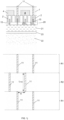
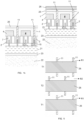
Figures 1a to 1l illustrate a number of steps of an embodiment of the method according to the invention by showing consecutive images of a small portion of a process wafer. Some figures include a section view and a plane view printed under the section view, with the position of the section plane indicated in the plane view. Others comprise only a section view, in which case the section plane is the same as the one indicated in the preceding drawings. Most plane views should not be regarded as horizontal sections nor as top views of the process wafer. The plane views are rather meant to illustrate the position of any component that is relevant for understanding the method steps. -
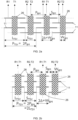
Figures 2a and 2b show additional images of staggered patterns of TSVs and their position with respect to back side power delivery tracks in an IC according to the invention, indicating a number of geometrical parameters of the pattern and of the power delivery tracks. -
Figures 3a to 3c illustrate key steps of an alternative method of producing an IC according to the invention. - In the following detailed description, an embodiment of an integrated circuit chip according to the invention is described. The IC chip is produced by processing a CMOS layout of finFET transistors arranged in standard cells on a semiconductor device wafer. However, the invention is not limited to this particular application field. As the invention is related also to a specific method for producing the chip according to the invention, this method is described first on a step-by-step basis, with reference to
Figures 1a to 1l . -
Figure 1a shows a small portion of a device wafer, comprising amonocrystalline Si layer 1, into which a number offins 2 and 2' have been produced by a known lithography and etch technique, applying etch masks 3. The width of the fins may be in the order of 10 nm or less. The two different types of hatching indicate different doping types (referred to also byrespective references 2 and 2'), typically p-type and n-type doping. In the embodiment shown, theSi layer 1 is a p-type layer, implanted with n-type dopants in consecutive well-areas 4. The well-areas 4 reach about half the depth of theSi layer 1 but could also reach to the back surface of the Si layer. The image is merely a schematic indication of the fact that adjacent p- and n-areas are created on the device wafer. This layout is typically used for producing pMOS and nMOS transistors arranged in multiple standard cells. In this example, alternate pairs of 2 p-type fins 2 and 2 n-type fins 2' are arranged with equal distances between the fins. This could also be groups of more than 2 p-type fins alternating with groups of more than 2 n-type fins. In the plane view ofFigure 1a , it is seen that the fin lengths differ and that the fins are arranged according to a pattern. The pattern shown is a random example of a possible fin pattern. - The
Si layer 1 is a monocrystalline top layer of a multi-layer device wafer comprising abase wafer 5, typically a Si wafer, and a thinetch stop layer 6, which could be a SiGe layer. The Si layer 1 (including the fins) preferably has a thickness less than 1 µm, for example about 500 nm. Theetch stop layer 6 may be a SiGe layer of about 50nm thick for example. Its function as an etch stop layer is to stop the etching of thebase wafer 5 for the removal of said base wafer from the back side, as will be explained later in this description. TheSiGe layer 6 and themonocrystalline Si layer 1 may be produced on aSi base wafer 5 by techniques well known in the art, preferably by epitaxial growth methods. An alternative would be to use a silicon-on-insulator (SOI) wafer, wherein the insulator layer plays the part of etch stop layer later in the process. Thefins 2, 2' are embedded in alayer 7 of dielectric material. Typically, this is a layer of silicon oxide (SiO2), also referred to as 'shallow trench isolation' oxide. We will hereafter refer to this layer as theSTI layer 7. - As shown in
Figure 1b , a plurality ofslits 10 is produced through theSTI layer 7 and through theSi layer 1, stopping in theSiGe layer 6. This is done by lithography and anisotropic etching, using a suitable etch technique known in the art. Theslits 10 are formed between fins of the same type (n or p) and no slits are formed between any p-type fin and its directly adjacent n-type fin. Theslits 10 are formed in a staggered pattern : theslits 10 formed between the n-type fins 2' are shifted in the longitudinal direction of the slits, with respect to theslits 10 formed between the p-type fins 2. This pattern is repeated across a given area of the wafer as illustrated in the plane view inFigure 1b . - In the embodiment shown, the etching of the
slits 10 is stopped inside theSiGe layer 6. Theslits 10 could also stop at the upper surface of theSiGe layer 6, or be etched fully through the SiGe layer 36 and slightly into thebase substrate 5. In any case, theslits 10 are formed essentially through the complete thickness of theSi layer 1. The width of theslits 10 is shown in the drawings to be in the same order of magnitude as the width of thefins 2,2', but may in reality exceed this width to some degree, whilst remaining in the order of tens of nanometres. Possibly, the spacing between the fins of the same type may be larger than shown in the drawings, to accommodate the processing of theslits 10. The length of theslits 10 is considerably higher than the width and may be in the order of several hundreds of nanometres. In the embodiment shown, the spacing between each pair of two alignedslits 10 is the same as the length of the slits. It is seen also that in the embodiment shown, two mutuallystaggered slits 10 do not overlap in their length direction. A limited degree of overlap is however allowable as will be described later. - With reference to
Figure 1c , theslits 10 are then filled with an electricallyconductive material 11. This involves the deposition of a dielectric liner conformally in theslits 10 and possibly a conformal barrier layer before depositing the conductive material, preferably a metal, for example W, Ru or Mo. The conformal layers are not shown in the drawings. Techniques for producing these layers and for filling theslits 10 with the conductive material are well known in the art. The upper surface of the wafer is planarized by a suitable technique known in the art such as CMP (chemical mechanical polishing), removing the etch masks 3 and exposing the conductive material on the upper surface of the wafer, in the form of a staggered pattern of conductive slit-shaped volumes 11'. - As seen in
Figure 1d , the volumes 11' are etched back to thereby form reducedvolumes 11, which will play the part of the TSV connections in the final IC, so from now on we will refer to them asTSVs 11. The abbreviation TSV is commonly understood as Through Silicon Via, but in the context of the present invention, the term is not limited to silicon, and may be understood as 'Through Semiconductor Via'. - The areas formed above the TSVs 11 (and limited in length to the length of the TSVs) are then filled with a
dielectric material 12, possibly SiO2, followed by another planarization step. Then a number of well-known CMOS front end of line process steps is performed, of which the result is illustrated in a simplified way inFigure 1e . This is the processing of source or drain (S/D)contacts 13 on thefins 2,2', in accordance with a given layout of standard cells arranged between theTSVs 11. The source ordrain contacts 13 are schematically drawn on top of the fins. In reality, theSTI layer 7 is etched back to expose the top of the fins, and the S/D contacts are formed thereon by epitaxial techniques well known in the art. As this technology is known and not the subject of the present invention however, the drawings have been simplified, showing S/D contacts on top of thefins 2,2' and embedded in adielectric layer 14. The S/D contacts 13 are also visible in the plane view inFigure 1e . The depicted distribution of thesecontacts 13 is not intended to represent a realistic layout, and merely illustrates a random arrangement of S/D contacts relative to the fin arrangement. - In a characteristic step of the method according to the invention, buried contact rails 15 are now produced, as shown in
Figure 1f . To this aim, trenches aligned to each line of mutually aligned TSVs 11 are first formed by lithography and etching, through thedielectric layers TSVs 11. These trenches may be somewhat narrower than theTSVs 11, as illustrated in the drawings. The trenches are filled (possibly after conformal deposition of a dielectric liner and barrier layer) with an electrically conductive material, preferably the same material as used for theTSVs 11. After filling the trenches, the top surface of the wafer is planarized. The result is a set ofparallel rails 15, each rail interconnecting a set ofTSVs 11 which are mutually aligned along their longitudinal direction. Therails 15 are destined to become connected alternately to the IC's supply voltage (hereafter referred to as Vdd) and to the reference voltage (hereafter referred to a Vss), so that twoadjacent rails 15 are configured to supply power to standard cells arranged between a Vdd rail and a Vss rail. The rails are therefore equivalent to the buried power rails described for example inEP3324436A1 andEP3651188A1 , where these rails are however formed prior to the formation of the S/D contacts and extend deeper into the device wafer, being buried in theSi layer 1 itself, whereas in the embodiment shown inFigure 1f , therails 15 are not buried in theSi layer 1, only in the dielectric materials present between two adjacent fins. - Before or after producing the
rails 15, further front end of line processing is performed, including the formation of gates and gate contacts in between pairs of source and drain contacts. These elements are not shown in the drawings but well-known to the skilled reader. The result is the 'front end of line portion' of the IC chip, indicated generally aslayer 20 inFigure 1f and subsequent figures. The '{' is merely an indicative sign of the location of theFEOL portion 20, without meaning to define an exact border. In theFEOL portion 20, theSTI layer 7 will play the well-known part of isolating active devices from each other. - Then the so-called M0 metal layer is formed, see
Figure 1g . This is the formation ofmetal conductors 16 which connect some of the source ordrain contacts 13 to the buried rails 15, in accordance once more with a given standard cell arrangement. As therails 15 are not buried deep in theSi layer 1, theM0 conductors 16 may be formed so as to contact the upper surface of therails 15 directly, as shown in the section view ofFigure 1g , by first planarizing the wafer to expose the S/D contacts 13 and therails 15, followed by a single damascene-type process for producing theconductors 16. This is advantageous compared to the more traditional deep buried rails, which require the formation of a narrow contact via between the rail and the M0 conductor. - After this, as illustrated in
Figure 1h , the back end of line process is performed, resulting in theBEOL portion 21 of the IC. As well-known in the art, this BEOL portion is a stack of interconnects comprising several metallization levels (M1,M2 etc), including a passivation layer on top (not shown). Theconductors 16 are indicated as part of the front end ofline portion 20 in the drawings. They could however be regarded as part of theBEOL portion 21. This distinction has no bearing on the characterising features of the present invention. - Back side processing is now performed, after flipping the wafer and bonding it to a
carrier wafer 22, preferably applying dielectric bonding layers 23 (shown as one bonded layer in the drawings) to thecarrier 22 and to theBEOL stack 21, as illustrated inFigure 1i . - The
base wafer 5 is removed by a thinning sequence that may comprise etching and/or grinding steps, ending with a highly selective etch step, preferably a wet etch in the case of a SiGeetch stop layer 6, that effectively stops when reaching theSiGe layer 6. Such highly selective etch recipes are well known for the selective etch of Si relative to SiGe as well as for other material combinations. Following this, theetch stop layer 6 itself is removed, resulting in the situation illustrated inFigure 1j , preferably with theTSVs 11 slightly protruding outward from the back surface of theSi layer 1. If necessary, the material of theSi layer 1 is slightly recessed in order to obtain this result. The plane view ofFigure 1j is in this case an actual top view, showing only what is visible on this back surface, namely the staggered pattern ofTSVs 11. It is seen that this pattern comprises at least one pair of rows R1 and R2 ofTSVs 11, extending in the direction perpendicular to theTSVs 11 and the power rails 15 and with theTSVs 11 of the second row R2 in a staggered position relative to the TSVs of the first row R1, i.e. the two rows comprise mutually staggered TSVs. Most ICs according to the invention will of course comprise many of such 'pairs of a first row and a second row of TSVs'. In the embodiment shown, a next pair of rows R1, R2 (only R1 is shown) follows under the first pair, and so on. In addition, the TSVs of all the 'first rows' R1 are aligned to each other, and the TSVs of all the 'second rows' R2 are aligned to each other and shifted with respect to the first rows by the same distance A indicated inFigure 1j , corresponding to the pitch of the array of parallel power rails 15. The length LTSV of the TSVs is preferably the same across the complete pattern. - With reference to
Figure 1k , a dielectric layer 25 (for example an oxide or nitride) is then deposited on the back surface of theSi layer 1, followed by a planarization, exposing theTSVs 11, as illustrated inFigure 1k . Finally, as shown inFigure 1l , electrically conductive power delivery tracks 26 are formed on the back side by a single damascene process, possibly using copper as the material for thetracks 26. The tracks are arranged transversely, in practice this will be essentially perpendicularly, with respect to theTSVs 11. As seen in the drawings, thetracks 26 are arranged in pairs T1, T2 of mutually parallel tracks, respectively overlapping and contacting two rows R1, R2 of mutually staggered TSVs. - In the language of appended
claim 1, it is thereby seen that theTSVs 11 are arranged in a staggered pattern, configured so that any one of the power delivery tracks 26 is connected to a first row of mutuallyparallel TSVs 11, and any power delivery track (26) directly adjacent to said power delivery track (i.e. the tracks on either side of the first track or on one side only, if the first one is located at the edge of the array of tracks 26) is connected to a second row of mutually parallel TSVs which are staggered relative to the TSVs of the first row, the second row being directly adjacent the first row. - In the finished IC, the
tracks 26 are alternately coupled to Vdd and Vss, i.e. every T1 coupled to Vdd and every T2 coupled to Vss, to thereby deliver these voltages alternately to theparallel rails 15, and to the standard cells arranged between each pair ofrails 15. On top of thetracks 26, further processing is done to produce a full power delivery network on the back side, connected to terminals of the finished IC that are configured to be coupled to external Vdd and Vss supply lines. These processing steps which are similar to BEOL processing are well known and therefore not described here in detail. At the end of the process, the wafer is singulated to form separate IC chips for example by cutting or sawing. The singulated portion of theSi layer 1 is then the semiconductor substrate of the chip, indicated by thesame reference numeral 1 in the appended claims, with active devices mounted on the front surface of thesubstrate 1, and a power delivery network on the back surface. - The arrangement of the
TSVs 11 as slit-shaped volumes of length LTSV aligned to the power rails 15 in a staggered pattern offers several advantages over the prior art solutions. It is a via-first approach, i.e. etching TSVs from the back side is not applied and the TSVs are aligned to the power rails 15, having a width that is essentially equal to or that only slightly exceeds the width of the power rails 15. This eliminates the problems related to wafer distortion and area overhead, as far as the processing and distribution of TSVs is concerned. In the direction of therails 15, the distance between two adjacent TSVs can be shortened compared to the TSVs produced by the TSV-last approach, because the area of the TSVs no longer has an influence on the available area for the active devices. - Importantly, the staggered pattern allows to combine a dense front side metal grid (power rails 15 close together), with a coarser back side power track arrangement, with relaxed overlay tolerance for patterning the back side power delivery tracks 26 relative to the
TSVs 11. The staggered pattern of TSVs allows adapting the length of the TSVs to a chosen width and pitch of thetracks 26 on the back side.Figures 2a and 2b are schematic images of two staggered TSV configurations. In both images, theTSVs 11 are now drawn horizontally and thetracks 26 vertically. The references R1,R2 and T1, T2 are again included to indicate the pairs of rows R1,R2 of TSVs and the corresponding pairs of tracks T1 ,T2. In the embodiment ofFigure 2a , the length LTSV of the TSVs is larger than the distance STSV between two adjacent TSVs, so that TSVs of R1 and R2 partially overlap with respect to each other, and with respect to the neighbouring row of TSVs. This is allowed, with the condition that a sufficient TSV length can be contacted by eachtrack 26. In the embodiment ofFigure 2b , the TSVs of R1 and R2 do not overlap each other nor the TSVs of neighbouring rows and the length LTSV is equal to the distance STSV. Likewise, the width WBM of thetracks 26 is equal to the distance SBM between two adjacent tracks. This embodiment enables the highest interconnect density. InFigures 2a and 2b the back to front overlay tolerance Δ is the overlay tolerance applied when processing thetracks 26 relative to the staggered pattern of the TSVs. This tolerance ensures that one track (T1 or T2) effectively contacts one row (R1 or R2), without contacting the TSVs of an adjacent row. In the processed IC, the position of the tracks may be shifted within this tolerance with respect to the ideal position shown in the drawings. - We will illustrate hereafter that a very relaxed overlay tolerance for patterning the back side power delivery tracks 26 can be applied, while still allowing a dense interconnect configuration. The following relations can be derived from the dimensions indicated in
Figures 2a and 2b : - ▪ The spacing STSV between the
TSVs 11 is defined as the sum of the backside metal width WBM and two times the back-to-front overlay accuracy Δ:
- ▪ The TSV length is given by: LTSV = PTSV - STSV = 2 PBM - STSV with PTSV the TSV pitch
- ▪ Therefore: LTSV = 2 PBM - WBM - 2 Δ, with PBM the pitch of the backside metal tracks
- ▪ In the embodiment of
Figure 2b , the TSV length equals the TSV spacing:

- Another way of producing an IC in accordance with the invention is described hereafter, with reference to
Figures 3a to 3c . According to this embodiment, and as illustrated inFigure 3a ,trenches 30 are produced at the locations where the buried power rails are to be formed, before producing the TSVs. Thesetrenches 30 are not etched through the complete thickness of theSi layer 1, but the etch is stopped before reaching the back surface of thislayer 1. Thetrenches 30 are formed along the complete length of a given fin pattern (said length being measured in the longitudinal direction of the fins). After this, as illustrated inFigure 3b , thetrenches 30 are further deepened to formelongate slits 31 at the TSV locations by a self-aligned etch, until reaching the back surface of theSi layer 1. The steps of etching thetrenches 30 and locally deepening these trenches typically involves substeps of depositing a dielectric liner on the walls and bottom of thetrenches 30, planarizing the wafer, forming a lithographic mask defining the TSV locations, removing the liner from the bottom of the trenches, and depositing a liner in theslits 31. These steps are described in more detail inEP3651188A1 , incorporated herein by reference. After forming a liner also at the bottom of theslits 31, an electrically conductive material is deposited in theslits 31 and in thetrenches 30 in a single deposition step (seeFigure 3c ), followed by etching back the conductive material in the trenches and depositing a dielectric 12. This results in the formation of buriedpower rails 15 andTSVs 11, the latter being arranged in the staggered pattern described above. After this, further steps for producing the IC are known as such, and include the formation of the source and drain contacts and further FEOL processing, M0 processing, BEOL processing and back side processing for producing the power delivery tracks 26. One difference with the method described earlier is that the power rails 15 are now buried deeper into theSi layer 1. This may require the formation of narrow via connections between the buriedpower rails 15 and theM0 conductors 16. - This approach for forming the staggered TSVs is a via-first approach, as basically described in
EP3651188A1 . The advantages of the staggered pattern as such and as described above for example in terms of the overlay tolerances, are however applicable regardless of the method by which the pattern has been produced. - The invention is not limited to an IC comprising fin-based devices. The staggered pattern of TSVs can be applied in combination with any type of known active devices on the front surface of the
Si layer 1. The devices could be nano-sheet based devices, well known in the art, wherein stacks of nano-sheets are processed on the front surface of theSi layer 1, said stacks have a similar profile to thefins 2 and 2' shown in the drawings. - While the invention has been illustrated and described in detail in the drawings and foregoing description, such illustration and description are to be considered illustrative or exemplary and not restrictive. Other variations to the disclosed embodiments can be understood and effected by those skilled in the art in practicing the claimed invention, from a study of the drawings, the disclosure and the appended claims. In the claims, the word "comprising" does not exclude other elements or steps, and the indefinite article "a" or "an" does not exclude a plurality. The mere fact that certain measures are recited in mutually different dependent claims does not indicate that a combination of these measures cannot be used to advantage. Any reference signs in the claims should not be construed as limiting the scope.
- The foregoing description details certain embodiments of the invention. It will be appreciated, however, that no matter how detailed the foregoing appears in text, the invention may be practiced in many ways, and is therefore not limited to the embodiments disclosed. It should be noted that the use of particular terminology when describing certain features or aspects of the invention should not be taken to imply that the terminology is being re-defined herein to be restricted to include any specific characteristics of the features or aspects of the invention with which that terminology is associated.
- Unless specifically specified, the description of a layer being present, deposited or produced 'on' another layer or substrate, includes the options of
- said layer being present, produced or deposited directly on, i.e. in physical contact with, said other layer or substrate, and
- said layer being present, produced or deposited on one or a stack of intermediate layers between said layer and said other layer or substrate.
Claims (11)
- An integrated circuit chip comprising :- a semiconductor substrate (1) having a front surface and a back surface,- active devices on the front surface of the substrate (1), isolated from each other by a dielectric layer (7),- mutually parallel power rails (15) extending in one direction and buried in the substrate (1) and/or in said dielectric layer (7),- through semiconductor via connections (11), hereafter referred to as TSVs, connecting the power rails (15) to the back surface of the substrate (1),- power delivery tracks (26) on the back surface of the substrate, oriented transversely with respect to the power rails (15), and connected to the power rails by said TSVs (11),wherein :- the power delivery tracks (26) are part of a power delivery network configured to be coupled to a supply voltage and to a reference voltage,- the power delivery tracks (26) are configured to be alternately connected to the supply voltage and to the reference voltage,- the TSVs (11) are arranged so that the power rails (15) are equally configured to be alternately connected to the supply voltage and the reference voltage,characterised in that :- the TSVs (11) are formed as elongate slit-shaped volumes aligned to the power rails (15),- the TSVs (11) are arranged in a staggered pattern, so that any one of the power delivery tracks (26) is connected to a first row of mutually parallel TSVs, and any power delivery track (26) directly adjacent to said power delivery track is connected to a second row of mutually parallel TSVs which are staggered relative to the TSVs of the first row, the second row being directly adjacent the first row.
- The IC chip according to claim 1, wherein all TSVs (1) of the staggered pattern have essentially the same length (LTSV), and wherein the distance (STSV) between two directly adjacent TSVs (11) which are mutually aligned along their longitudinal direction is essentially the same across the staggered pattern.
- The IC chip according to claim 2, wherein the distance (STSV) between two directly adjacent TSVs (11) which are mutually aligned along their longitudinal direction is smaller than or equal to the length (LTSV) of the TSVs.
- The IC chip according to claim 3, wherein the distance (STSV) between two directly adjacent TSVs (11) which are mutually aligned along their longitudinal direction is essentially equal to the length (LTSV) of the TSVs, and wherein all the power delivery tracks (26) have essentially the same width (WBM) and are configured by an essentially constant distance (SBM) between directly adjacent power delivery tracks (26).
- The IC chip according to claim 4, wherein the width (WBM) of the power delivery tracks (26) is essentially equal to the distance (SBM) between directly adjacent power delivery tracks.
- The IC chip according to any one of the preceding claims, wherein the power rails (15) are buried only in said dielectric layer (7) and not in the substrate (1).
- The IC chip according to any one of the preceding claims, wherein the active devices are fin-based devices or nano-sheet based devices and wherein the power rails (15) run parallel to the fins (2,2') or to the nano-sheets.
- The IC chip according to any one of the preceding claims, wherein the power delivery tracks (26) are essentially perpendicular to the buried power rails (15).
- A method for producing an IC chip according to any one of the preceding claims, the method comprising the steps of :- providing a device wafer comprising a semiconductor layer (1) on its upper surface,- producing slits (10) in the semiconductor layer, according to said staggered pattern, the slits (10) going through the complete thickness of the semiconductor layer (1),- filling the slits (10) with an electrically conductive material,- etching back the conductive material in the slits (10) from the front surface of the semiconductor layer (1) to thereby produce the staggered TSVs (11) and depositing a dielectric material (12) on top of the TSVs,- producing active devices including contacts (13) on the front surface of the semiconductor layer (1), said active devices being isolated from each other by a dielectric layer (7), said active devices defining at least part of a front end of line portion (20) of the IC chip,- by etching trenches from the front side of the device wafer and into said dielectric layer (7) and by filling said trenches with an electrically conductive material, producing the power rails (15) aligned to the TSVs (11), so that any two directly adjacent power rails (15) are connected respectively to two groups of mutually staggered TSVs (11),- producing electrical conductors (16) on the front side of the device wafer, said conductors (16) connecting the power rails (15) to a plurality of the contacts (13), producing a back end of line portion (21) of the IC chip on the front end of line portion (20),- flipping the wafer and bonding it to a carrier wafer (22),- thinning the device wafer until the TSVs (11) are exposed on the back surface of the semiconductor layer (1),- producing the power delivery tracks (26) transversely with respect to the TSVs (11).
- The method according to claim 9, wherein the device wafer comprises a base wafer (5), an etch stop layer (6) on the base wafer, and said semiconductor layer (1) on the etch stop layer, wherein the etch stop function of the etch stop layer (6) is related to stopping an etch process applied during said step of thinning the device wafer.
- The method according to claim 9, wherein the power delivery tracks (26) are essentially perpendicular to the power rails (15).
Priority Applications (2)
| Application Number | Priority Date | Filing Date | Title |
|---|---|---|---|
| EP21197018.1A EP4152381B1 (en) | 2021-09-16 | 2021-09-16 | An integrated circuit chip comprising back-side power delivery tracks |
| US17/932,582 US12557634B2 (en) | 2021-09-16 | 2022-09-15 | Integrated circuit chip including back side power delivery tracks |
Applications Claiming Priority (1)
| Application Number | Priority Date | Filing Date | Title |
|---|---|---|---|
| EP21197018.1A EP4152381B1 (en) | 2021-09-16 | 2021-09-16 | An integrated circuit chip comprising back-side power delivery tracks |
Publications (2)
| Publication Number | Publication Date |
|---|---|
| EP4152381A1 true EP4152381A1 (en) | 2023-03-22 |
| EP4152381B1 EP4152381B1 (en) | 2024-10-30 |
Family
ID=77864349
Family Applications (1)
| Application Number | Title | Priority Date | Filing Date |
|---|---|---|---|
| EP21197018.1A Active EP4152381B1 (en) | 2021-09-16 | 2021-09-16 | An integrated circuit chip comprising back-side power delivery tracks |
Country Status (2)
| Country | Link |
|---|---|
| US (1) | US12557634B2 (en) |
| EP (1) | EP4152381B1 (en) |
Families Citing this family (1)
| Publication number | Priority date | Publication date | Assignee | Title |
|---|---|---|---|---|
| US11929325B2 (en) * | 2021-08-18 | 2024-03-12 | Qualcomm Incorporated | Mixed pitch track pattern |
Citations (5)
| Publication number | Priority date | Publication date | Assignee | Title |
|---|---|---|---|---|
| EP3324436A1 (en) | 2016-11-21 | 2018-05-23 | IMEC vzw | An integrated circuit chip with power delivery network on the backside of the chip |
| EP3651188A1 (en) | 2018-11-12 | 2020-05-13 | IMEC vzw | A method for contacting a buried interconnect rail from the back side of an ic |
| EP3742487A1 (en) * | 2019-05-23 | 2020-11-25 | IMEC vzw | An integrated circuit with backside power delivery network and backside transistor |
| US20210098369A1 (en) * | 2019-09-30 | 2021-04-01 | Taiwan Semiconductor Manufacturing Co., Ltd. | Via Rail Structure |
| US20210202384A1 (en) * | 2019-12-31 | 2021-07-01 | Taiwan Semiconductor Manufacturing Company Limited | Dual power structure with efficient layout |
Family Cites Families (8)
| Publication number | Priority date | Publication date | Assignee | Title |
|---|---|---|---|---|
| US6355950B1 (en) * | 1998-09-23 | 2002-03-12 | Intel Corporation | Substrate interconnect for power distribution on integrated circuits |
| US8034702B2 (en) | 2007-08-16 | 2011-10-11 | Micron Technology, Inc. | Methods of forming through substrate interconnects |
| US8035198B2 (en) | 2008-08-08 | 2011-10-11 | International Business Machines Corporation | Through wafer via and method of making same |
| KR101459597B1 (en) | 2013-05-03 | 2014-11-10 | (주)실리콘화일 | Method for forming through silicon via |
| KR101436553B1 (en) | 2013-05-06 | 2014-09-01 | (주)티에프아이 | Semiconductor appratus having through silicon via structure and manufacturing method thereof |
| US11195797B2 (en) * | 2019-05-21 | 2021-12-07 | Samsung Electronics Co., Ltd. | Applications of buried power rails |
| US11735525B2 (en) * | 2019-10-21 | 2023-08-22 | Tokyo Electron Limited | Power delivery network for CFET with buried power rails |
| US12557377B2 (en) * | 2021-05-13 | 2026-02-17 | Tokyo Electron Limited | Inverted cross-couple for top-tier FET for multi-tier gate-on-gate 3DI |
-
2021
- 2021-09-16 EP EP21197018.1A patent/EP4152381B1/en active Active
-
2022
- 2022-09-15 US US17/932,582 patent/US12557634B2/en active Active
Patent Citations (5)
| Publication number | Priority date | Publication date | Assignee | Title |
|---|---|---|---|---|
| EP3324436A1 (en) | 2016-11-21 | 2018-05-23 | IMEC vzw | An integrated circuit chip with power delivery network on the backside of the chip |
| EP3651188A1 (en) | 2018-11-12 | 2020-05-13 | IMEC vzw | A method for contacting a buried interconnect rail from the back side of an ic |
| EP3742487A1 (en) * | 2019-05-23 | 2020-11-25 | IMEC vzw | An integrated circuit with backside power delivery network and backside transistor |
| US20210098369A1 (en) * | 2019-09-30 | 2021-04-01 | Taiwan Semiconductor Manufacturing Co., Ltd. | Via Rail Structure |
| US20210202384A1 (en) * | 2019-12-31 | 2021-07-01 | Taiwan Semiconductor Manufacturing Company Limited | Dual power structure with efficient layout |
Also Published As
| Publication number | Publication date |
|---|---|
| EP4152381B1 (en) | 2024-10-30 |
| US12557634B2 (en) | 2026-02-17 |
| US20230080522A1 (en) | 2023-03-16 |
Similar Documents
| Publication | Publication Date | Title |
|---|---|---|
| US10636739B2 (en) | Integrated circuit chip with power delivery network on the backside of the chip | |
| US11257764B2 (en) | Integrated circuit with backside power delivery network and backside transistor | |
| US10985057B2 (en) | Method for contacting a buried interconnect rail of an integrated circuit chip from the back side of the IC | |
| JP7486058B2 (en) | Replacement buried power rails in rear power supply. | |
| JP7704265B2 (en) | Semiconductor device and its manufacturing method | |
| US12494424B2 (en) | Interconnect structure of a semiconductor component and methods for producing the structure | |
| US12538779B2 (en) | Method for producing a buried interconnect rail of an integrated circuit chip | |
| US20230207660A1 (en) | 3d single crystal silicon transistor design integrated with 3d wafer transfer technology and metal first approach | |
| EP4187600B1 (en) | A semiconductor component comprising back side i/o signal routing | |
| US12368078B2 (en) | Dual-side power rail design and method of making same | |
| EP4152381B1 (en) | An integrated circuit chip comprising back-side power delivery tracks | |
| US12107132B2 (en) | Source/drain contact positioning under power rail | |
| US8436425B2 (en) | SOI semiconductor device comprising substrate diodes having a topography tolerant contact structure | |
| US12362236B2 (en) | Method of producing an integrated circuit chip including a back-side power delivery network | |
| US20250029872A1 (en) | Method for producing an interconnect via | |
| CN119028978A (en) | Integrated circuit structure and method for manufacturing the same | |
| EP4287246A1 (en) | A method for producing an interconnect rail for contacting a semiconductor device from the back side | |
| US20240120257A1 (en) | Layer-By-Layer Formation Of Through-Substrate Via | |
| WO2025215433A1 (en) | Self aligned backside contacts compatible with passive devices |
Legal Events
| Date | Code | Title | Description |
|---|---|---|---|
| PUAI | Public reference made under article 153(3) epc to a published international application that has entered the european phase |
Free format text: ORIGINAL CODE: 0009012 |
|
| STAA | Information on the status of an ep patent application or granted ep patent |
Free format text: STATUS: THE APPLICATION HAS BEEN PUBLISHED |
|
| AK | Designated contracting states |
Kind code of ref document: A1 Designated state(s): AL AT BE BG CH CY CZ DE DK EE ES FI FR GB GR HR HU IE IS IT LI LT LU LV MC MK MT NL NO PL PT RO RS SE SI SK SM TR |
|
| STAA | Information on the status of an ep patent application or granted ep patent |
Free format text: STATUS: REQUEST FOR EXAMINATION WAS MADE |
|
| 17P | Request for examination filed |
Effective date: 20231208 |
|
| RBV | Designated contracting states (corrected) |
Designated state(s): AL AT BE BG CH CY CZ DE DK EE ES FI FR GB GR HR HU IE IS IT LI LT LU LV MC MK MT NL NO PL PT RO RS SE SI SK SM TR |
|
| GRAP | Despatch of communication of intention to grant a patent |
Free format text: ORIGINAL CODE: EPIDOSNIGR1 |
|
| STAA | Information on the status of an ep patent application or granted ep patent |
Free format text: STATUS: GRANT OF PATENT IS INTENDED |
|
| RIC1 | Information provided on ipc code assigned before grant |
Ipc: H01L 27/02 20060101ALI20240527BHEP Ipc: H01L 23/535 20060101ALI20240527BHEP Ipc: H01L 21/74 20060101ALI20240527BHEP Ipc: H01L 21/768 20060101ALI20240527BHEP Ipc: H01L 27/118 20060101ALI20240527BHEP Ipc: H01L 21/8238 20060101ALI20240527BHEP Ipc: H01L 21/84 20060101ALI20240527BHEP Ipc: H01L 27/092 20060101ALI20240527BHEP Ipc: H01L 27/12 20060101ALI20240527BHEP Ipc: H01L 23/528 20060101AFI20240527BHEP |
|
| INTG | Intention to grant announced |
Effective date: 20240611 |
|
| RIN1 | Information on inventor provided before grant (corrected) |
Inventor name: VELOSO, ANABELA Inventor name: JOURDAIN, ANNE Inventor name: BEYNE, ERIC |
|
| GRAS | Grant fee paid |
Free format text: ORIGINAL CODE: EPIDOSNIGR3 |
|
| GRAA | (expected) grant |
Free format text: ORIGINAL CODE: 0009210 |
|
| STAA | Information on the status of an ep patent application or granted ep patent |
Free format text: STATUS: THE PATENT HAS BEEN GRANTED |
|
| AK | Designated contracting states |
Kind code of ref document: B1 Designated state(s): AL AT BE BG CH CY CZ DE DK EE ES FI FR GB GR HR HU IE IS IT LI LT LU LV MC MK MT NL NO PL PT RO RS SE SI SK SM TR |
|
| REG | Reference to a national code |
Ref country code: GB Ref legal event code: FG4D |
|
| REG | Reference to a national code |
Ref country code: CH Ref legal event code: EP |
|
| REG | Reference to a national code |
Ref country code: DE Ref legal event code: R096 Ref document number: 602021020929 Country of ref document: DE |
|
| REG | Reference to a national code |
Ref country code: IE Ref legal event code: FG4D |
|
| P01 | Opt-out of the competence of the unified patent court (upc) registered |
Free format text: CASE NUMBER: APP_59001/2024 Effective date: 20241029 |
|
| REG | Reference to a national code |
Ref country code: LT Ref legal event code: MG9D |
|
| REG | Reference to a national code |
Ref country code: NL Ref legal event code: MP Effective date: 20241030 |
|
| PG25 | Lapsed in a contracting state [announced via postgrant information from national office to epo] |
Ref country code: IS Free format text: LAPSE BECAUSE OF FAILURE TO SUBMIT A TRANSLATION OF THE DESCRIPTION OR TO PAY THE FEE WITHIN THE PRESCRIBED TIME-LIMIT Effective date: 20250228 Ref country code: PT Free format text: LAPSE BECAUSE OF FAILURE TO SUBMIT A TRANSLATION OF THE DESCRIPTION OR TO PAY THE FEE WITHIN THE PRESCRIBED TIME-LIMIT Effective date: 20250228 Ref country code: HR Free format text: LAPSE BECAUSE OF FAILURE TO SUBMIT A TRANSLATION OF THE DESCRIPTION OR TO PAY THE FEE WITHIN THE PRESCRIBED TIME-LIMIT Effective date: 20241030 |
|
| PG25 | Lapsed in a contracting state [announced via postgrant information from national office to epo] |
Ref country code: FI Free format text: LAPSE BECAUSE OF FAILURE TO SUBMIT A TRANSLATION OF THE DESCRIPTION OR TO PAY THE FEE WITHIN THE PRESCRIBED TIME-LIMIT Effective date: 20241030 Ref country code: NL Free format text: LAPSE BECAUSE OF FAILURE TO SUBMIT A TRANSLATION OF THE DESCRIPTION OR TO PAY THE FEE WITHIN THE PRESCRIBED TIME-LIMIT Effective date: 20241030 |
|
| REG | Reference to a national code |
Ref country code: AT Ref legal event code: MK05 Ref document number: 1737810 Country of ref document: AT Kind code of ref document: T Effective date: 20241030 |
|
| PG25 | Lapsed in a contracting state [announced via postgrant information from national office to epo] |
Ref country code: BG Free format text: LAPSE BECAUSE OF FAILURE TO SUBMIT A TRANSLATION OF THE DESCRIPTION OR TO PAY THE FEE WITHIN THE PRESCRIBED TIME-LIMIT Effective date: 20241030 |
|
| PG25 | Lapsed in a contracting state [announced via postgrant information from national office to epo] |
Ref country code: ES Free format text: LAPSE BECAUSE OF FAILURE TO SUBMIT A TRANSLATION OF THE DESCRIPTION OR TO PAY THE FEE WITHIN THE PRESCRIBED TIME-LIMIT Effective date: 20241030 |
|
| PG25 | Lapsed in a contracting state [announced via postgrant information from national office to epo] |
Ref country code: NO Free format text: LAPSE BECAUSE OF FAILURE TO SUBMIT A TRANSLATION OF THE DESCRIPTION OR TO PAY THE FEE WITHIN THE PRESCRIBED TIME-LIMIT Effective date: 20250130 |
|
| PG25 | Lapsed in a contracting state [announced via postgrant information from national office to epo] |
Ref country code: GR Free format text: LAPSE BECAUSE OF FAILURE TO SUBMIT A TRANSLATION OF THE DESCRIPTION OR TO PAY THE FEE WITHIN THE PRESCRIBED TIME-LIMIT Effective date: 20250131 Ref country code: LV Free format text: LAPSE BECAUSE OF FAILURE TO SUBMIT A TRANSLATION OF THE DESCRIPTION OR TO PAY THE FEE WITHIN THE PRESCRIBED TIME-LIMIT Effective date: 20241030 Ref country code: AT Free format text: LAPSE BECAUSE OF FAILURE TO SUBMIT A TRANSLATION OF THE DESCRIPTION OR TO PAY THE FEE WITHIN THE PRESCRIBED TIME-LIMIT Effective date: 20241030 |
|
| PG25 | Lapsed in a contracting state [announced via postgrant information from national office to epo] |
Ref country code: PL Free format text: LAPSE BECAUSE OF FAILURE TO SUBMIT A TRANSLATION OF THE DESCRIPTION OR TO PAY THE FEE WITHIN THE PRESCRIBED TIME-LIMIT Effective date: 20241030 |
|
| PG25 | Lapsed in a contracting state [announced via postgrant information from national office to epo] |
Ref country code: RS Free format text: LAPSE BECAUSE OF FAILURE TO SUBMIT A TRANSLATION OF THE DESCRIPTION OR TO PAY THE FEE WITHIN THE PRESCRIBED TIME-LIMIT Effective date: 20250130 |
|
| PG25 | Lapsed in a contracting state [announced via postgrant information from national office to epo] |
Ref country code: SM Free format text: LAPSE BECAUSE OF FAILURE TO SUBMIT A TRANSLATION OF THE DESCRIPTION OR TO PAY THE FEE WITHIN THE PRESCRIBED TIME-LIMIT Effective date: 20241030 |
|
| PG25 | Lapsed in a contracting state [announced via postgrant information from national office to epo] |
Ref country code: DK Free format text: LAPSE BECAUSE OF FAILURE TO SUBMIT A TRANSLATION OF THE DESCRIPTION OR TO PAY THE FEE WITHIN THE PRESCRIBED TIME-LIMIT Effective date: 20241030 |
|
| PG25 | Lapsed in a contracting state [announced via postgrant information from national office to epo] |
Ref country code: EE Free format text: LAPSE BECAUSE OF FAILURE TO SUBMIT A TRANSLATION OF THE DESCRIPTION OR TO PAY THE FEE WITHIN THE PRESCRIBED TIME-LIMIT Effective date: 20241030 |
|
| PG25 | Lapsed in a contracting state [announced via postgrant information from national office to epo] |
Ref country code: RO Free format text: LAPSE BECAUSE OF FAILURE TO SUBMIT A TRANSLATION OF THE DESCRIPTION OR TO PAY THE FEE WITHIN THE PRESCRIBED TIME-LIMIT Effective date: 20241030 |
|
| PG25 | Lapsed in a contracting state [announced via postgrant information from national office to epo] |
Ref country code: SK Free format text: LAPSE BECAUSE OF FAILURE TO SUBMIT A TRANSLATION OF THE DESCRIPTION OR TO PAY THE FEE WITHIN THE PRESCRIBED TIME-LIMIT Effective date: 20241030 |
|
| PG25 | Lapsed in a contracting state [announced via postgrant information from national office to epo] |
Ref country code: CZ Free format text: LAPSE BECAUSE OF FAILURE TO SUBMIT A TRANSLATION OF THE DESCRIPTION OR TO PAY THE FEE WITHIN THE PRESCRIBED TIME-LIMIT Effective date: 20241030 |
|
| PG25 | Lapsed in a contracting state [announced via postgrant information from national office to epo] |
Ref country code: IT Free format text: LAPSE BECAUSE OF FAILURE TO SUBMIT A TRANSLATION OF THE DESCRIPTION OR TO PAY THE FEE WITHIN THE PRESCRIBED TIME-LIMIT Effective date: 20241030 |
|
| REG | Reference to a national code |
Ref country code: DE Ref legal event code: R097 Ref document number: 602021020929 Country of ref document: DE |
|
| PLBE | No opposition filed within time limit |
Free format text: ORIGINAL CODE: 0009261 |
|
| STAA | Information on the status of an ep patent application or granted ep patent |
Free format text: STATUS: NO OPPOSITION FILED WITHIN TIME LIMIT |
|
| PG25 | Lapsed in a contracting state [announced via postgrant information from national office to epo] |
Ref country code: SE Free format text: LAPSE BECAUSE OF FAILURE TO SUBMIT A TRANSLATION OF THE DESCRIPTION OR TO PAY THE FEE WITHIN THE PRESCRIBED TIME-LIMIT Effective date: 20241030 |
|
| 26N | No opposition filed |
Effective date: 20250731 |
|
| PGFP | Annual fee paid to national office [announced via postgrant information from national office to epo] |
Ref country code: DE Payment date: 20250820 Year of fee payment: 5 |
|
| REG | Reference to a national code |
Ref country code: DE Ref legal event code: R079 Ref document number: 602021020929 Country of ref document: DE Free format text: PREVIOUS MAIN CLASS: H01L0023528000 Ipc: H10W0020430000 |
|
| REG | Reference to a national code |
Ref country code: CH Ref legal event code: H13 Free format text: ST27 STATUS EVENT CODE: U-0-0-H10-H13 (AS PROVIDED BY THE NATIONAL OFFICE) Effective date: 20260504 |
|
| PG25 | Lapsed in a contracting state [announced via postgrant information from national office to epo] |
Ref country code: LU Free format text: LAPSE BECAUSE OF NON-PAYMENT OF DUE FEES Effective date: 20250916 |
|
| GBPC | Gb: european patent ceased through non-payment of renewal fee |
Effective date: 20250916 |
|
| REG | Reference to a national code |
Ref country code: BE Ref legal event code: MM Effective date: 20250930 |
|
| PG25 | Lapsed in a contracting state [announced via postgrant information from national office to epo] |
Ref country code: LT Free format text: LAPSE BECAUSE OF FAILURE TO SUBMIT A TRANSLATION OF THE DESCRIPTION OR TO PAY THE FEE WITHIN THE PRESCRIBED TIME-LIMIT Effective date: 20241030 |
|
| PG25 | Lapsed in a contracting state [announced via postgrant information from national office to epo] |
Ref country code: MC Free format text: LAPSE BECAUSE OF FAILURE TO SUBMIT A TRANSLATION OF THE DESCRIPTION OR TO PAY THE FEE WITHIN THE PRESCRIBED TIME-LIMIT Effective date: 20241030 |
|
| PG25 | Lapsed in a contracting state [announced via postgrant information from national office to epo] |
Ref country code: GB Free format text: LAPSE BECAUSE OF NON-PAYMENT OF DUE FEES Effective date: 20250916 |
|
| PG25 | Lapsed in a contracting state [announced via postgrant information from national office to epo] |
Ref country code: BE Free format text: LAPSE BECAUSE OF NON-PAYMENT OF DUE FEES Effective date: 20250930 Ref country code: IE Free format text: LAPSE BECAUSE OF NON-PAYMENT OF DUE FEES Effective date: 20250916 Ref country code: CH Free format text: LAPSE BECAUSE OF NON-PAYMENT OF DUE FEES Effective date: 20250930 |
|
| PG25 | Lapsed in a contracting state [announced via postgrant information from national office to epo] |
Ref country code: FR Free format text: LAPSE BECAUSE OF NON-PAYMENT OF DUE FEES Effective date: 20250930 |