EP4152363A1 - Methods of forming dislocation enhanced strain in nmos structures - Google Patents
Methods of forming dislocation enhanced strain in nmos structures Download PDFInfo
- Publication number
- EP4152363A1 EP4152363A1 EP22198320.8A EP22198320A EP4152363A1 EP 4152363 A1 EP4152363 A1 EP 4152363A1 EP 22198320 A EP22198320 A EP 22198320A EP 4152363 A1 EP4152363 A1 EP 4152363A1
- Authority
- EP
- European Patent Office
- Prior art keywords
- source
- drain
- region
- crystal semiconductor
- strained
- Prior art date
- Legal status (The legal status is an assumption and is not a legal conclusion. Google has not performed a legal analysis and makes no representation as to the accuracy of the status listed.)
- Pending
Links
Images



Classifications
-
- H—ELECTRICITY
- H10—SEMICONDUCTOR DEVICES; ELECTRIC SOLID-STATE DEVICES NOT OTHERWISE PROVIDED FOR
- H10D—INORGANIC ELECTRIC SEMICONDUCTOR DEVICES
- H10D30/00—Field-effect transistors [FET]
- H10D30/60—Insulated-gate field-effect transistors [IGFET]
- H10D30/791—Arrangements for exerting mechanical stress on the crystal lattice of the channel regions
- H10D30/797—Arrangements for exerting mechanical stress on the crystal lattice of the channel regions being in source or drain regions, e.g. SiGe source or drain
-
- H—ELECTRICITY
- H10—SEMICONDUCTOR DEVICES; ELECTRIC SOLID-STATE DEVICES NOT OTHERWISE PROVIDED FOR
- H10D—INORGANIC ELECTRIC SEMICONDUCTOR DEVICES
- H10D30/00—Field-effect transistors [FET]
- H10D30/01—Manufacture or treatment
- H10D30/021—Manufacture or treatment of FETs having insulated gates [IGFET]
- H10D30/024—Manufacture or treatment of FETs having insulated gates [IGFET] of fin field-effect transistors [FinFET]
-
- H—ELECTRICITY
- H10—SEMICONDUCTOR DEVICES; ELECTRIC SOLID-STATE DEVICES NOT OTHERWISE PROVIDED FOR
- H10D—INORGANIC ELECTRIC SEMICONDUCTOR DEVICES
- H10D30/00—Field-effect transistors [FET]
- H10D30/01—Manufacture or treatment
- H10D30/021—Manufacture or treatment of FETs having insulated gates [IGFET]
- H10D30/027—Manufacture or treatment of FETs having insulated gates [IGFET] of lateral single-gate IGFETs
-
- H—ELECTRICITY
- H10—SEMICONDUCTOR DEVICES; ELECTRIC SOLID-STATE DEVICES NOT OTHERWISE PROVIDED FOR
- H10D—INORGANIC ELECTRIC SEMICONDUCTOR DEVICES
- H10D30/00—Field-effect transistors [FET]
- H10D30/60—Insulated-gate field-effect transistors [IGFET]
- H10D30/611—Insulated-gate field-effect transistors [IGFET] having multiple independently-addressable gate electrodes influencing the same channel
-
- H—ELECTRICITY
- H10—SEMICONDUCTOR DEVICES; ELECTRIC SOLID-STATE DEVICES NOT OTHERWISE PROVIDED FOR
- H10D—INORGANIC ELECTRIC SEMICONDUCTOR DEVICES
- H10D30/00—Field-effect transistors [FET]
- H10D30/60—Insulated-gate field-effect transistors [IGFET]
- H10D30/62—Fin field-effect transistors [FinFET]
-
- H—ELECTRICITY
- H10—SEMICONDUCTOR DEVICES; ELECTRIC SOLID-STATE DEVICES NOT OTHERWISE PROVIDED FOR
- H10D—INORGANIC ELECTRIC SEMICONDUCTOR DEVICES
- H10D30/00—Field-effect transistors [FET]
- H10D30/60—Insulated-gate field-effect transistors [IGFET]
- H10D30/751—Insulated-gate field-effect transistors [IGFET] having composition variations in the channel regions
-
- H—ELECTRICITY
- H10—SEMICONDUCTOR DEVICES; ELECTRIC SOLID-STATE DEVICES NOT OTHERWISE PROVIDED FOR
- H10D—INORGANIC ELECTRIC SEMICONDUCTOR DEVICES
- H10D62/00—Semiconductor bodies, or regions thereof, of devices having potential barriers
- H10D62/01—Manufacture or treatment
- H10D62/021—Forming source or drain recesses by etching e.g. recessing by etching and then refilling
-
- H—ELECTRICITY
- H10—SEMICONDUCTOR DEVICES; ELECTRIC SOLID-STATE DEVICES NOT OTHERWISE PROVIDED FOR
- H10D—INORGANIC ELECTRIC SEMICONDUCTOR DEVICES
- H10D62/00—Semiconductor bodies, or regions thereof, of devices having potential barriers
- H10D62/10—Shapes, relative sizes or dispositions of the regions of the semiconductor bodies; Shapes of the semiconductor bodies
- H10D62/117—Shapes of semiconductor bodies
- H10D62/118—Nanostructure semiconductor bodies
- H10D62/119—Nanowire, nanosheet or nanotube semiconductor bodies
- H10D62/121—Nanowire, nanosheet or nanotube semiconductor bodies oriented parallel to substrates
-
- H—ELECTRICITY
- H10—SEMICONDUCTOR DEVICES; ELECTRIC SOLID-STATE DEVICES NOT OTHERWISE PROVIDED FOR
- H10D—INORGANIC ELECTRIC SEMICONDUCTOR DEVICES
- H10D62/00—Semiconductor bodies, or regions thereof, of devices having potential barriers
- H10D62/10—Shapes, relative sizes or dispositions of the regions of the semiconductor bodies; Shapes of the semiconductor bodies
- H10D62/17—Semiconductor regions connected to electrodes not carrying current to be rectified, amplified or switched, e.g. channel regions
- H10D62/213—Channel regions of field-effect devices
- H10D62/221—Channel regions of field-effect devices of FETs
- H10D62/235—Channel regions of field-effect devices of FETs of IGFETs
-
- H—ELECTRICITY
- H10—SEMICONDUCTOR DEVICES; ELECTRIC SOLID-STATE DEVICES NOT OTHERWISE PROVIDED FOR
- H10D—INORGANIC ELECTRIC SEMICONDUCTOR DEVICES
- H10D62/00—Semiconductor bodies, or regions thereof, of devices having potential barriers
- H10D62/50—Physical imperfections
- H10D62/53—Physical imperfections the imperfections being within the semiconductor body
-
- H—ELECTRICITY
- H10—SEMICONDUCTOR DEVICES; ELECTRIC SOLID-STATE DEVICES NOT OTHERWISE PROVIDED FOR
- H10D—INORGANIC ELECTRIC SEMICONDUCTOR DEVICES
- H10D64/00—Electrodes of devices having potential barriers
- H10D64/01—Manufacture or treatment
- H10D64/013—Manufacture or treatment of electrodes having a conductor capacitively coupled to a semiconductor by an insulator
- H10D64/01356—Manufacture or treatment of electrodes having a conductor capacitively coupled to a semiconductor by an insulator the insulator being formed after the semiconductor body, the semiconductor being a Group IV material and not being silicon, e.g. Ge, SiGe or SiGeC
-
- H—ELECTRICITY
- H10—SEMICONDUCTOR DEVICES; ELECTRIC SOLID-STATE DEVICES NOT OTHERWISE PROVIDED FOR
- H10D—INORGANIC ELECTRIC SEMICONDUCTOR DEVICES
- H10D62/00—Semiconductor bodies, or regions thereof, of devices having potential barriers
- H10D62/80—Semiconductor bodies, or regions thereof, of devices having potential barriers characterised by the materials
- H10D62/82—Heterojunctions
- H10D62/822—Heterojunctions comprising only Group IV materials heterojunctions, e.g. Si/Ge heterojunctions
Definitions
- CMOS transistor improvement may involve controlling the strain state of the transistor channel.
- an NMOS transistor portion and a PMOS transistor portion may require differing types of channel strain requirements.
- the NMOS channel may require a tensile strain in the channel region
- the PMOS channel may require a compressive strain in the channel region.
- Those methods/structures may include forming a thin silicon germanium material on a source/drain opening of a device comprising silicon, wherein multiple dislocations are formed in the silicon germanium material, and then forming a source/drain material on the thin silicon germanium material, wherein the dislocations induce source/drain dislocations throughout the source/drain material.
- the embodiments herein enable strained channel devices, wherein the soorce/drain structures may induce a tensile strain in a channel region of the device.
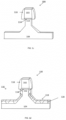
- FIGS. 1a-1e illustrate views of embodiments of forming microelectronic structures, such as NMOS strained silicon transistor structures, for example,
- a device 100 may comprise a substrate portion 104 ( FIG. 1a , top view).
- the substrate 104 may comprise at least one of a silicon, a non-silicon material, a single crystal silicon material, a polysilicon material, a piezoelectric material, III-V material and/or other electromechanical substrate material.
- the device 100 may comprise a portion of a planar transistor, a multi-gate transistor, such as a tri-gate and/or finFET transistor, and a nanowire structure.
- the device 100 may further comprise a gate structure 102, which may comprise a portion of a transistor gate structure 102, such as an NMOS transistor gate structure.
- the device 100 may further comprise source/drain structures 108.
- the source/drain structures 108 may comprise silicon fin structures, in an embodiment, which may be separated from each other by dielectric material 106.
- the dielectric material 106 may comprise a STI (silicon trench isolation) material in an embodiment.
- the dielectric material 106 may provide isolation between the fin structures 108 and the gate electrode 102.
- a channel portion of the device 100 may be disposed underneath the gate structure 102.
- source/drain structures/fins 104 may be removed from the substrate portion 104 of the device 100 ( FIG. 1b , top view).
- an etch process 109 may be employed, such as a wet or dry etch, for example, wherein the silicon of the source/drain/fin structures 108 are removed, leaving an opening 110 in the substrate 104 adjacent the STI 106.
- a channel portion of the silicon underneath the gate electrode remains intact, that is, it remains unetched by the removal process/etch process 109.
- FIG. 1c depicts a cross sectional view of the device 100, wherein the source/drain fins 104 are removed and the openings 110 are exposed in a portion of the substrate 104.
- a channel region 112 is disposed underneath the gate electrode 102, wherein a gate dielectric layer 116 is disposed between the gate electrode 102 and the channel region 112.
- a spacer material 116 may be disposed on the gate electrode 102.
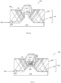
- a dislocation nucleation layer/material 118 may be formed in the openings 110 ( FIG. 1d , cross section).
- the dislocation nucleation layer 118 may be selectively grown using epitaxial growth in the openings 110 on the substrate 104 in the source/drain regions.
- the dislocation nucleation layer 118 may comprise a silicon germanium layer 118.
- the dislocation nucleation layer 118 may be grown such that a plurality of dislocations may form in the dislocation nucleation layer 118.
- the dislocation nucleation layer 118 may comprise a thickness of about 2 to about 50 nm.
- the dislocation nucleation layer 118 may produce a net strain that comprises a tensile strain.
- the lattice constant of the dislocation nucleation layer 118 may comprise a lattice constant that is much larger than the lattice constant of the substrate 104.
- the lattice constant may comprise between 5.43 and 5.66 ⁇ for silicon germanium alloy, and 5.43 ⁇ for a silicon substrate
- the dislocation nucleation layer 118 may be formed by epitaxial growth as an initial layer on the silicon portion of the source/drain openings 110.
- the source/drain openings may comprise NMOS source/drain openings 110.
- the dislocation nucleation layer 118 when the dislocation nucleation layer 118 comprises a silicon germanium material, the silicon germanium may comprise a germanium concentration of between about ten percent to about eighty percent. In another embodiment, the silicon germanium may be doped with at least one of phosphorus and arsenic In an embodiment, the phosphorus may comprise a concentration between about 10 16 cm -3 and 10 21 cm -3 . In an embodiment, the arsenic may comprise a concentration between about 10 16 cm -3 and 10 21 cm -3 . In an embodiment, the dislocation nucleation layer 118 may comprise a silicon germanium, phosphorus, arsenic concentration that is substantially evenly distributed throughout the dislocation nucleation layer 118.
- the dislocation nucleation layer 118 may comprise a lower portion comprising a silicon germanium, phosphorus, and arsenic concentration that is substantially evenly distributed in a lower portion of the dislocation nucleation layer 118, and may comprise an upper portion comprising substantially a silicon phosphorus concentration.
- the dislocation nucleation layer 118 may be grown in the openings 110 as an undoped silicon germanium material that may be subsequently doped by one of an ion implantation and a diffusion doping from a dopant source.
- the dislocation nucleation layer 118 may be formed using a molecular beam epitaxial method (MBE), such as a gas source (GS)-MBE method.
- MBE molecular beam epitaxial method
- a rapid thermal chemical vapor deposition (RT-CVD) reactor or a CVD reactor may be used to grow the dislocation nucleation layer 118.
- a process to grow the dislocation nucleation layer 118 may include the use of silane, germane, digermane, phosphine, and hydrochloric acid with a hydrogen carrier gas. A temperature of 700 degrees Celsius and a pressure of 20 Torr may be employed.
- the parameters for the dislocation nucleation layer 118 growth process may vary depending upon the particular application. In an embodiment, the growth parameters may be optimized for the formation of a plurality of defects. In an embodiment, a large number of dislocations/defects 120 may be formed/initiated at the interface between the substrate 104 and the dislocation nucleation layer 118.
- a source/drain material 122 may be selectively formed on the dislocation nucleation layer 118 after sufficient defect 120 formation in the dislocation nucleation layer118 ( FIG. 1e , cross section).
- the source/drain material 122 may comprise of silicon or silicon carbon alloy material.
- the source/drain material 122 may comprise a thickness of about 5 to about 100 nm.
- the dislocation nucleation layer 118 may provide a source of dislocations/defects 120 that may induce source/drain dislocations 124 in the source/drain material/structure 122.
- the dislocation nucleation layer 118 and the source/drain material 122 may comprise a source/drain fin structure 123.
- the dislocations 124 in the source/drain material 122 may continue to propagate up towards a free surface 125 of the source/drain material 122.
- the multiple dislocations 124 disposed in the source/drain material 122 may cause a flipping of the strain imparted by the lattice mismatched dislocation nucleation layer 118 from a compressive to a tensile strain in the channel region 112.
- overlapping strain fields from each dislocation 124 can overcome the compressive stress that may be present in the dislocation nucleation layer 118, such as a silicon germanium layer 118.
- the source/drain material 122 may impart a tensile strain on the channel region 112 along a conduction direction for the device 100, which may comprise a transistor device in embodiments.
- the device 100 may comprise circuitry elements such as transistor structures including planar, trigate and nanowire transistor structures, and any other suitable circuitry elements.
- the circuitry elements may comprise logic ciicuitry for use in a processor die, for example.
- Metallization layers and insulative material may be included in the device 100, as well as conductive contacts/bumps that may couple metal layers/interconnects to external devices transistor device.
- the type of elements included in the device 100 may comprise any suitable type of circuit elements, according to the particular application.
- FIG. 2 depicts a cross-sectional views of an embodiment comprising a device structure 200, wherein the device comprises a nanowire
- the device 200 such as a nanowire device 200, may comprise a in a substrate 204 disposed below a channel region 212.
- a dislocation nucleation layer 218 may comprise a plurality of defects/dislocations 220.
- a source/drain material 222 may comprise a plurality of defects/dislocations 224.
- a gate electrode 202 may be disposed on a gate dielectric 214.
- a nanowire material 203. such as silicon, may be disposed underneath the gate dielectric 214.
- a wrap around gate dielectric 205 may be disposed beneath the wrap around nanowire material 203.
- a wrap around gate electrode 207. may be disposed underneath the wrap around gate dielectric 205.
- the channel region comprises an induced strain from the dislocations from the source/drain material 222.
- the device 100 of the embodiments may be coupled with any suitable type of package structures capable of providing electrical communications between a microelectronic device, such as a die and a next-level component to which the package structures may be coupled (e.g., a circuit board).
- the device may be coupled with a package structure that may comprise any suitable type of package structures capable of providing electrical communication between a die and an upper integrated circuit (IC) package coupled with the device layer.
- IC integrated circuit
- the device described in the various Figures herein may comprise a portion of a silicon logic die or a memory die, for example, or any type of suitable microelectronic device/die.
- the device of the embodiments may further comprise a plurality of dies, which may be stacked upon one another, depending upon the particular embodiment.
- the device may be located attached/embedded on either the front side, back side or on/in some combination of the front and back sides of a package structure.
- the device may be partially or fully embedded in a package structure.
- the various embodiments of the strained channel devices herein enable strain transfer from the source/drain region of an NMOS source/drain region to an NMOS channel region.
- the strain transfer is accomplished through the use of dislocation strain fields in the NMOS source/drain regions.
- Some prior art methods of achieving channel strain have involved employing buffer layers of mismatched lattice constant materials under the channel region, and employing dopants in the source/drain region.
- the embodiments herein include employing a dislocation nucleation layer, such as silicon germanium, to propagate overlapping strain fields that induce tensile strain in the channel region. Since the growth takes place only within the source/drain region, the embodiments, avoid performance degradation into the channel as seen when utilizing buffer layers, as in the prior art.
- the system 300 includes a number of components disposed on a mainboard 310 or other circuit board.
- Mainboard 310 includes a first side 312 and an opposing second side 314, and various components may be disposed on either one or both of the first end second sides 312, 314.
- the comparing system 300 includes a package structure 340 disposed on the mainboard's first side 312, wherein the package structure 340 may comprise any of the device structures, such as the transistor device structures of the embodiments described herein.
- System 300 mav comprise any type of computing system, such as, for example, a hand-held or mobile computing device (e.g., a cell phone, a smart phone, a mobile internet device, a music player, a tablet computer, a laptop computer, a nettop computer, etc.).
- a hand-held or mobile computing device e.g., a cell phone, a smart phone, a mobile internet device, a music player, a tablet computer, a laptop computer, a nettop computer, etc.
- the disclosed embodiments are not limited to hand-held and other mobile computing devices and these embodiments may find application in other types of computing systems, such as desk-top computers and servers.
- Mainboard 310 may comprise any suitable type of circuit board or other substrate capable of providing electrical communication between one or more of the various components disposed on the board.
- the mainboard 310 comprises a printed circuit board (PCB) comprising multiple metal layers separated from one another by a layer of dielectric material and interconnected by electrically conductive vias. Any one or more of the metal layers may be formed in a desired circuit pattern to route - perhaps in conjunction with other metal layers - electrical signals between the components coupled with the board 310.
- PCB printed circuit board
- mainboard 310 may comprise any other suitable substrate.
- one or more additional components may be disposed on either one or both sides 312, 314 of the mainboard 310.
- components 301a may be disposed on the first side 312 of the mainboard 310
- components 301b may be disposed on the mainboard's opposing side 314.
- Additional components that may be disposed on the mainboard 310 include other IC devices (e.g., processing devices, memory devices, signal processing devices, wireless communication devices, graphics controllers and/or drivers, audio processors and/or controllers, etc.), power delivery components (e.g., a voltage regulator and/or other power management devices, a power supply such as a battery, and/or passive devices such as a capacitor), and one or more user interface devices (e.g., an audio input device, an audio output device, a keypad or other data entry device such as a touch screen display, and/or a graphics display, etc.). as well as any combination of these and/or other devices.
- IC devices e.g., processing devices, memory devices, signal processing devices, wireless communication devices, graphics controllers and/or drivers, audio processors and/or controllers, etc.
- power delivery components e.g., a voltage regulator and/or other power management devices, a power supply such as a battery, and/or passive devices such as a capacitor
- the computing system 300 includes a radiation shield. In a further embodiment, the computing system 300 includes a cooling solution. In yet another embodiment, the computing system 300 includes an antenna. In yet a farther embodiment, the assembly 300 may be disposed within a housing or case. Where the mainboard 310 is disposed within a housing, some of the components of computer system 300 - e.g., a user interface device, such as a display or keypad, and/or a power supply, such as a battery - may be electrically coupled with the mainboard 310 (and/or a component disposed on this board) but may be mechanically coupled with the housing.
- a user interface device such as a display or keypad
- a power supply such as a battery
- FIG. 4 is a schematic of a computer system 400 according to an embodiment.
- the computer system 400 (also referred to as the electronic system 400) as depicted can embody/include a package structure that includes any of the several disclosed device embodiments and their equivalents as set forth in this disclosure.
- the computer system 400 may be a mobile device such as a netbook computer.
- the computer system 400 may be a mobile device such as a wireless smart phone.
- the computer system 400 may be a desktop computer.
- the computer system 400 may be a hand-held reader.
- the computer system 400 may be integral to an automobile.
- the computer system 400 may be integral to a television.
- the electronic system 400 is a computer system that includes a system bus 420 to electrically couple the various components of the electronic system 400.
- the system bus 420 is a single bus or any combination of busses according to various embodiments
- the electronic system 400 includes a voltage source 430 that provides power to the integrated circuit 410.
- the voltage source 430 supplies current to the integrated circuit 410 through the system bus 420
- the integrated circuit 410 is electrically, communicatively coupled to the system bus 420 and includes any circuit, or combination of circuits according to an embodiment, including the package/device structures of the various embodiments included herein.
- the integrated circuit 410 includes a processor 412 that can include any type of packaging structures including vertical passive structures according to the embodiments herein.
- the processor 412 may mean any type of circuit such as, but not limited to, a microprocessor, a microcontroller, a graphics processor, a digital signal processor, or another processor
- the processor 412 includes any of the embodiments of the package structures disclosed herein.
- SRAM embodiments are found in memory caches of the processor.
- circuits that can be included in the integrated circuit 410 are a custom circuit or an application-specific integrated circuit (ASIC), such as a communications circuit 414 for use in wireless devices such as cellular telephones, smart phones, pagers, portable computers, two-way radios, and similar electronic systems.
- ASIC application-specific integrated circuit
- the processor 412 includes on-die memory 416 such as static random-access memory (SRAM).
- the processor 412 includes embedded on-die memory 416 such as embedded dynamic random-access memory (eDRAM).
- the integrated circuit 410 is complemented with a subsequent integrated circuit 411.
- the dual integrated circuit 411 includes embedded on-die memory 417 such as eDRAM.
- the dual integrated circuit 411 includes an RFIC dual processor 413 and a dual communications circuit 415 and dual on-die memory 417 such as SRAM.
- the dual communications circuit 415 may be configured for RF processing.
- the electronic system 400 also includes an external memory 440 that in turn may include one or more memory elements suitable to the particular application, such as a main memory 442 in the form of RAM. one or more hard drives 444, and/or one or more drives that handle removable media 446, such as diskettes, compact disks (CDs), digital variable disks (DVDs), flash memory drives, and other removable media known in the art.
- the external memory 440 may also be embedded memory 448.
- the electronic system 400 also includes a display device 450, and an audio output 460.
- the electronic system 400 includes an input device such as a controller 470 that may be a keyboard, mouse, touch pad, keypad, trackball, game controller, microphone, voice-recognition device, or any other input device that inputs information into the electronic system 400.
- an input device 470 includes a camera.
- an input device 470 includes a digital sound recorder In an embodiment, an input device 470 includes a camera and a digital sound recorder.
Landscapes
- Metal-Oxide And Bipolar Metal-Oxide Semiconductor Integrated Circuits (AREA)
- Insulated Gate Type Field-Effect Transistor (AREA)
- Thin Film Transistor (AREA)
- Recrystallisation Techniques (AREA)
Abstract
Description
- As microelectronic technology advances for higher performance, integration of high performance transistor devices. such as CMOS transistors devices, becomes increasingly important. CMOS transistor improvement may involve controlling the strain state of the transistor channel. Within a CMOS device, an NMOS transistor portion and a PMOS transistor portion may require differing types of channel strain requirements. For example, the NMOS channel may require a tensile strain in the channel region, while the PMOS channel may require a compressive strain in the channel region.
- White the specification concludes with claims particularly pointing out and distinctly claiming certain embodiments, the advantages of these embodiments can be more readily ascertained from the following description of the invention when read in conjunction with the accompanying drawings in which:
-
FIGS. 1a-1e represent top and cross-scctional views of structures according to various embodiments. -
FIG. 2 represents a cross-sectional view of a structure according to embodiments. -
FIG. 3 represents a cross-sectional view of a system according to embodiments. -
FIG. 4 represents a schematic of a system according to embodiments. - In the following detailed description, reference is made to the accompanying drawings that show, by way of illustration, specific embodiments in which the methods and structures may be practiced. These embodiments are described in sufficient detail to enable those skilled in the art to practice the embodiments, It is to be understood that the various embodiments, although different, are not necessarily mutually exclusive. For example, a particular feature, structure, or characteristic described herein, in connection with one embodiment, may be implemented within other embodiments without departing from the spirit and scope of the embodiments. In addition, it is to be understood that the location or arrangement of individual elements within each disclosed embodiment may be modified without departing from the spirit and scope of the embodiments. The following detailed description is, therefore, not to be taken in a limiting sense, and the scope of the embodiments is defined only by the appended claims, appropriately interpreted, along with the full range of equivalents to which the claims are entitled. In the drawings, like numerals may refer to the same or similar functionality throughout the several views.
- Methods and associated structures of forming and utilizing microelectronic structures, such as device structures comprising strained source/drain structures, are described. Those methods/structures may include forming a thin silicon germanium material on a source/drain opening of a device comprising silicon, wherein multiple dislocations are formed in the silicon germanium material, and then forming a source/drain material on the thin silicon germanium material, wherein the dislocations induce source/drain dislocations throughout the source/drain material. The embodiments herein enable strained channel devices, wherein the soorce/drain structures may induce a tensile strain in a channel region of the device.
-
FIGS. 1a-1e illustrate views of embodiments of forming microelectronic structures, such as NMOS strained silicon transistor structures, for example, In an embodiment, adevice 100 may comprise a substrate portion 104 (FIG. 1a , top view). In an embodiment, thesubstrate 104 may comprise at least one of a silicon, a non-silicon material, a single crystal silicon material, a polysilicon material, a piezoelectric material, III-V material and/or other electromechanical substrate material. In an embodiment, thedevice 100 may comprise a portion of a planar transistor, a multi-gate transistor, such as a tri-gate and/or finFET transistor, and a nanowire structure. - The
device 100 may further comprise agate structure 102, which may comprise a portion of atransistor gate structure 102, such as an NMOS transistor gate structure. Thedevice 100 may further comprise source/drain structures 108. The source/drain structures 108 may comprise silicon fin structures, in an embodiment, which may be separated from each other bydielectric material 106. Thedielectric material 106 may comprise a STI (silicon trench isolation) material in an embodiment. Thedielectric material 106 may provide isolation between thefin structures 108 and thegate electrode 102. In an embodiment, a channel portion of thedevice 100 may be disposed underneath thegate structure 102. - In an embodiment, source/drain structures/
fins 104 may be removed from thesubstrate portion 104 of the device 100 (FIG. 1b , top view). In an embodiment, anetch process 109 may be employed, such as a wet or dry etch, for example, wherein the silicon of the source/drain/fin structures 108 are removed, leaving anopening 110 in thesubstrate 104 adjacent theSTI 106. A channel portion of the silicon underneath the gate electrode remains intact, that is, it remains unetched by the removal process/etch process 109.FIG. 1c depicts a cross sectional view of thedevice 100, wherein the source/drain fins 104 are removed and theopenings 110 are exposed in a portion of thesubstrate 104. Achannel region 112 is disposed underneath thegate electrode 102, wherein a gatedielectric layer 116 is disposed between thegate electrode 102 and thechannel region 112. Aspacer material 116 may be disposed on thegate electrode 102. - A dislocation nucleation layer/
material 118 may be formed in the openings 110 (FIG. 1d , cross section). In an embodiment, thedislocation nucleation layer 118 may be selectively grown using epitaxial growth in theopenings 110 on thesubstrate 104 in the source/drain regions. In an embodiment, thedislocation nucleation layer 118 may comprise asilicon germanium layer 118. Thedislocation nucleation layer 118 may be grown such that a plurality of dislocations may form in thedislocation nucleation layer 118. In an embodiment, thedislocation nucleation layer 118 may comprise a thickness of about 2 to about 50 nm. - The
dislocation nucleation layer 118 may produce a net strain that comprises a tensile strain. In an embodiment, the lattice constant of thedislocation nucleation layer 118 mav be mismatched (and may contribute to stress dislocation formation) as compared with thesubstrate 104. In an embodiment, thedislocation nucleation layer 118 may comprise a lattice constant that is much larger than the lattice constant of thesubstrate 104. for example, the lattice constant may comprise between 5.43 and 5.66 Å for silicon germanium alloy, and 5.43Å for a silicon substrate In an embodiment, thedislocation nucleation layer 118 may be formed by epitaxial growth as an initial layer on the silicon portion of the source/drain openings 110. In an embodiment, the source/drain openings may comprise NMOS source/drain openings 110. - In an embodiment, when the
dislocation nucleation layer 118 comprises a silicon germanium material, the silicon germanium may comprise a germanium concentration of between about ten percent to about eighty percent. In another embodiment, the silicon germanium may be doped with at least one of phosphorus and arsenic In an embodiment, the phosphorus may comprise a concentration between about 1016 cm-3 and 1021 cm-3. In an embodiment, the arsenic may comprise a concentration between about 1016 cm-3 and 1021 cm-3. In an embodiment, thedislocation nucleation layer 118 may comprise a silicon germanium, phosphorus, arsenic concentration that is substantially evenly distributed throughout thedislocation nucleation layer 118. - In another embodiment, the
dislocation nucleation layer 118 may comprise a lower portion comprising a silicon germanium, phosphorus, and arsenic concentration that is substantially evenly distributed in a lower portion of thedislocation nucleation layer 118, and may comprise an upper portion comprising substantially a silicon phosphorus concentration. In another embodiment, thedislocation nucleation layer 118 may be grown in theopenings 110 as an undoped silicon germanium material that may be subsequently doped by one of an ion implantation and a diffusion doping from a dopant source. In another embodiment, thedislocation nucleation layer 118 may be formed using a molecular beam epitaxial method (MBE), such as a gas source (GS)-MBE method. - In an embodiment, a rapid thermal chemical vapor deposition (RT-CVD) reactor or a CVD reactor may be used to grow the
dislocation nucleation layer 118. In an embodiment, a process to grow thedislocation nucleation layer 118 may include the use of silane, germane, digermane, phosphine, and hydrochloric acid with a hydrogen carrier gas. A temperature of 700 degrees Celsius and a pressure of 20 Torr may be employed. The parameters for thedislocation nucleation layer 118 growth process may vary depending upon the particular application. In an embodiment, the growth parameters may be optimized for the formation of a plurality of defects. In an embodiment, a large number of dislocations/defects 120 may be formed/initiated at the interface between thesubstrate 104 and thedislocation nucleation layer 118. - In an embodiment, a source/
drain material 122 may be selectively formed on thedislocation nucleation layer 118 aftersufficient defect 120 formation in the dislocation nucleation layer118 (FIG. 1e , cross section). In an embodiment, the source/drain material 122 may comprise of silicon or silicon carbon alloy material. In an embodiment, the source/drain material 122 may comprise a thickness of about 5 to about 100 nm. In an embodiment, thedislocation nucleation layer 118 may provide a source of dislocations/defects 120 that may induce source/drain dislocations 124 in the source/drain material/structure 122.In an embodiment, thedislocation nucleation layer 118 and the source/drain material 122 may comprise a source/drain fin structure 123. - In an embodiment, the
dislocations 124 in the source/drain material 122 may continue to propagate up towards a free surface 125 of the source/drain material 122. In an embodiments themultiple dislocations 124 disposed in the source/drain material 122 may cause a flipping of the strain imparted by the lattice mismatcheddislocation nucleation layer 118 from a compressive to a tensile strain in thechannel region 112. In an embodiment, overlapping strain fields from eachdislocation 124 can overcome the compressive stress that may be present in thedislocation nucleation layer 118, such as asilicon germanium layer 118. In an embodiment, the source/drain material 122 may impart a tensile strain on thechannel region 112 along a conduction direction for thedevice 100, which may comprise a transistor device in embodiments. - In an embodiment, the
device 100 may comprise circuitry elements such as transistor structures including planar, trigate and nanowire transistor structures, and any other suitable circuitry elements. The circuitry elements may comprise logic ciicuitry for use in a processor die, for example. Metallization layers and insulative material may be included in thedevice 100, as well as conductive contacts/bumps that may couple metal layers/interconnects to external devices transistor device. The type of elements included in thedevice 100 may comprise any suitable type of circuit elements, according to the particular application. -
FIG. 2 depicts a cross-sectional views of an embodiment comprising adevice structure 200, wherein the device comprises a nanowire In an embodiment, thedevice 200, such as ananowire device 200, may comprise a in asubstrate 204 disposed below a channel region 212. Adislocation nucleation layer 218 may comprise a plurality of defects/dislocations 220. A source/drain material 222 may comprise a plurality of defects/dislocations 224. Agate electrode 202 may be disposed on agate dielectric 214. Ananowire material 203. such as silicon, may be disposed underneath thegate dielectric 214. A wrap aroundgate dielectric 205 may be disposed beneath the wrap aroundnanowire material 203. A wrap around gate electrode 207. may be disposed underneath the wrap aroundgate dielectric 205. The channel region comprises an induced strain from the dislocations from the source/drain material 222. - In an embodiment, the
device 100 of the embodiments may be coupled with any suitable type of package structures capable of providing electrical communications between a microelectronic device, such as a die and a next-level component to which the package structures may be coupled (e.g., a circuit board). In another embodiment, the device may be coupled with a package structure that may comprise any suitable type of package structures capable of providing electrical communication between a die and an upper integrated circuit (IC) package coupled with the device layer. - The device described in the various Figures herein may comprise a portion of a silicon logic die or a memory die, for example, or any type of suitable microelectronic device/die. In some embodiments the device of the embodiments may further comprise a plurality of dies, which may be stacked upon one another, depending upon the particular embodiment. In some cases the device may be located attached/embedded on either the front side, back side or on/in some combination of the front and back sides of a package structure. In an embodiment the device may be partially or fully embedded in a package structure.
- The various embodiments of the strained channel devices herein enable strain transfer from the source/drain region of an NMOS source/drain region to an NMOS channel region. The strain transfer is accomplished through the use of dislocation strain fields in the NMOS source/drain regions. Some prior art methods of achieving channel strain have involved employing buffer layers of mismatched lattice constant materials under the channel region, and employing dopants in the source/drain region. The embodiments herein include employing a dislocation nucleation layer, such as silicon germanium, to propagate overlapping strain fields that induce tensile strain in the channel region. Since the growth takes place only within the source/drain region, the embodiments, avoid performance degradation into the channel as seen when utilizing buffer layers, as in the prior art.
- Turning now to
FIG. 3 . illustrated is an embodiment of acomputing system 300. Thesystem 300 includes a number of components disposed on amainboard 310 or other circuit board.Mainboard 310 includes afirst side 312 and an opposingsecond side 314, and various components may be disposed on either one or both of the first end second sides 312, 314. In the illustrated embodiment, the comparingsystem 300 includes apackage structure 340 disposed on the mainboard'sfirst side 312, wherein thepackage structure 340 may comprise any of the device structures, such as the transistor device structures of the embodiments described herein. -
System 300 mav comprise any type of computing system, such as, for example, a hand-held or mobile computing device (e.g., a cell phone, a smart phone, a mobile internet device, a music player, a tablet computer, a laptop computer, a nettop computer, etc.). However, the disclosed embodiments are not limited to hand-held and other mobile computing devices and these embodiments may find application in other types of computing systems, such as desk-top computers and servers. - Mainboard 310 may comprise any suitable type of circuit board or other substrate capable of providing electrical communication between one or more of the various components disposed on the board. In one embodiment, for example, the
mainboard 310 comprises a printed circuit board (PCB) comprising multiple metal layers separated from one another by a layer of dielectric material and interconnected by electrically conductive vias. Any one or more of the metal layers may be formed in a desired circuit pattern to route - perhaps in conjunction with other metal layers - electrical signals between the components coupled with theboard 310. However, it should be understood that the disclosed embodiments are not limited to the above~described PCB and, further, thatmainboard 310 may comprise any other suitable substrate. - In addition to the
package structure 340, one or more additional components may be disposed on either one or bothsides mainboard 310. By way of example, as shown in the figures,components 301a may be disposed on thefirst side 312 of themainboard 310, andcomponents 301b may be disposed on the mainboard's opposingside 314. Additional components that may be disposed on themainboard 310 include other IC devices (e.g., processing devices, memory devices, signal processing devices, wireless communication devices, graphics controllers and/or drivers, audio processors and/or controllers, etc.), power delivery components (e.g., a voltage regulator and/or other power management devices, a power supply such as a battery, and/or passive devices such as a capacitor), and one or more user interface devices (e.g., an audio input device, an audio output device, a keypad or other data entry device such as a touch screen display, and/or a graphics display, etc.). as well as any combination of these and/or other devices. - In one embodiment, the
computing system 300 includes a radiation shield. In a further embodiment, thecomputing system 300 includes a cooling solution. In yet another embodiment, thecomputing system 300 includes an antenna. In yet a farther embodiment, theassembly 300 may be disposed within a housing or case. Where themainboard 310 is disposed within a housing, some of the components of computer system 300 - e.g., a user interface device, such as a display or keypad, and/or a power supply, such as a battery - may be electrically coupled with the mainboard 310 (and/or a component disposed on this board) but may be mechanically coupled with the housing. -
FIG. 4 is a schematic of acomputer system 400 according to an embodiment. The computer system 400 (also referred to as the electronic system 400) as depicted can embody/include a package structure that includes any of the several disclosed device embodiments and their equivalents as set forth in this disclosure. Thecomputer system 400 may be a mobile device such as a netbook computer. Thecomputer system 400 may be a mobile device such as a wireless smart phone. Thecomputer system 400 may be a desktop computer. Thecomputer system 400 may be a hand-held reader. Thecomputer system 400 may be integral to an automobile. Thecomputer system 400 may be integral to a television. - In an embodiment, the
electronic system 400 is a computer system that includes a system bus 420 to electrically couple the various components of theelectronic system 400. The system bus 420 is a single bus or any combination of busses according to various embodiments Theelectronic system 400 includes a voltage source 430 that provides power to theintegrated circuit 410. In some embodiments, the voltage source 430 supplies current to theintegrated circuit 410 through the system bus 420 - The
integrated circuit 410 is electrically, communicatively coupled to the system bus 420 and includes any circuit, or combination of circuits according to an embodiment, including the package/device structures of the various embodiments included herein. In an embodiment, theintegrated circuit 410 includes aprocessor 412 that can include any type of packaging structures including vertical passive structures according to the embodiments herein. As used herein, theprocessor 412 may mean any type of circuit such as, but not limited to, a microprocessor, a microcontroller, a graphics processor, a digital signal processor, or another processor In an embodiment, theprocessor 412 includes any of the embodiments of the package structures disclosed herein. In an embodiment, SRAM embodiments are found in memory caches of the processor. - Other types of circuits that can be included in the
integrated circuit 410 are a custom circuit or an application-specific integrated circuit (ASIC), such as acommunications circuit 414 for use in wireless devices such as cellular telephones, smart phones, pagers, portable computers, two-way radios, and similar electronic systems. In an embodiment, theprocessor 412 includes on-die memory 416 such as static random-access memory (SRAM). In an embodiment, theprocessor 412 includes embedded on-die memory 416 such as embedded dynamic random-access memory (eDRAM). - In an embodiment, the
integrated circuit 410 is complemented with a subsequentintegrated circuit 411. In an embodiment, the dualintegrated circuit 411 includes embedded on-die memory 417 such as eDRAM. The dualintegrated circuit 411 includes an RFICdual processor 413 and adual communications circuit 415 and dual on-die memory 417 such as SRAM. Thedual communications circuit 415 may be configured for RF processing. - At least one
passive device 480 is coupled to the subsequentintegrated circuit 411. In an embodiment, theelectronic system 400 also includes anexternal memory 440 that in turn may include one or more memory elements suitable to the particular application, such as amain memory 442 in the form of RAM. one or morehard drives 444, and/or one or more drives that handleremovable media 446, such as diskettes, compact disks (CDs), digital variable disks (DVDs), flash memory drives, and other removable media known in the art. Theexternal memory 440 may also be embeddedmemory 448. In an embodiment, theelectronic system 400 also includes adisplay device 450, and anaudio output 460. In an embodiment, theelectronic system 400 includes an input device such as acontroller 470 that may be a keyboard, mouse, touch pad, keypad, trackball, game controller, microphone, voice-recognition device, or any other input device that inputs information into theelectronic system 400. In an embodiment, aninput device 470 includes a camera. In an embodiment, aninput device 470 includes a digital sound recorder In an embodiment, aninput device 470 includes a camera and a digital sound recorder. - Although the foregoing description has specified certain steps and materials that may be used in the methods of the embodiments, those skilled in the art will appreciate that many modifications and substitutions may be made. Accordingly, it is intended that all such modifications, alterations, substitutions and additions be considered to fall within the spirit and scope of the embodiments as defined by the appended claims. In addition, the Figures provided herein illustrate only portions of exemplary microelectronic devices and associated package structures that pertain to the practice of the embodiments. Thus the embodiments are not limited to the structures described herein.
The preferred aspects of the present disclosure may be summarized as follows: - 1. A method of forming a structure comprising:
- forming openings in source/drain regions of a device disposed on a substrate;
- forming a dislocation nucleation material in the source/drain openings, wherein the dislocation nucleation material comprises a lattice constant that is mismatched with a substrate lattice constant, and wherein a plurality of dislocations form in the dislocation nucleation material; and
- forming a source/drain material on the dislocation material, wherein a plurality of source/drain dislocations are formed in the source/drain material.
- 2. The method of aspect 1 further comprising wherein a channel region remains underneath a gate electrode of the device, and wherein the channel region is not removed during the opening formation process.
- 3. The method of aspect 1 further comprising wherein the dislocation nucleation material induces a tensile stress in the source/drain material, and wherein the device comprises one of a trigate, a finFET and a nanowire structure.
- 4. The method of aspect 1 further comprising wherein the dislocation nucleation material comprises a silicon germanium material that is selectively grown in the source/drain openings.
- 5. The method of aspect 4 further comprising wherein the silicon germanium material is epitaxially grown, wherein the plurality of dislocations formed in the silicon germanium material produce a tensile strain in the source/drain material that induces a tensile strain in a channel region adjacent the source/drain material.
- 6. The method of aspect 1 further comprising wherein the source/drain material comprises a silicon phosphorus material, and wherein the source/drain material is selectively grown on a silicon portion of the substrate.
- 7. The method of aspect 4 further comprising wherein the amount of germanium in the silicon germanium material comprises a range of about 40 percent to about 80 percent by weight.
- 8. The method of aspect 7 further comprising wherein the dislocation nocleation material further comprises at least one of phosphorus and arsenic.
- 9. The method of aspect 4 further comprising wherein the silicon germanium comprises a continuous distribution of arsenic and phosphorus.
- 10. The method of aspect 1 further comprising wherein the dislocation material comprises a lower portion comprising silicon germanium, phosphorus and arsenic and an upper portion comprising silicon and phosphorus.
- 11. The method of aspect 1 further comprising wherein the silicon germanium is doped by one of ion implantation and diffusion doping.
- 12. A method of forming a structure comprising:
- forming a thin silicon germanium material on a source/drain opening of a device comprising silicon, wherein multiple dislocations are formed in the silicon germanium material; and
- forming a source/drain material on the thin silicon germanium material, wherein the dislocations induce source/drain dislocations throughout the source/drain material.
- 13. The method of aspect 12 further comprising wherein overlapping strain fields in the source/drain material impart a tensile strain to a channel region of the device adjacent the source/drain material.
- 14. The method of aspect 13 further comprising wherein the source/drain material comprises a silicon fin structure of a portion of one of a trigate transistor, a planar transistor, and a nanowire structure.
- 15. The method of aspect 12 further comprising wherein the source/drain material comprises a lattice constant that is mismatched with the lattice constant of the substrate.
- 16. The method of aspect 12 further comprising wherein the structure comprises a portion of an NMOS structure.
- 17. A structure comprising:
- a dislocation nucleation material disposed on a silicon material in a source/drain region of a device, wherein the dislocation nucleation material comprises a lattice constant that is lower than a lattice constant of a substrate portion of the device; and
- a source/drain material disposed on the dislocation nucleation material, wherein the source/drain material comprises a lattice constant that is lower than the dislocation nucleation material; and
- a plurality of dislocations disposed in the source/drain material.
- 18. The structure of aspect 17 further comprising wherein the dislocation nucleation material comprises an epitaxial silicon germanium.
- 19. The structure of aspect 17 further comprising wherein the dislocation nucleation material comprises a thickness between 2 to 50nm.
- 20. The structure of aspect 17 further comprising wherein the device comprises a portion of one of a trigate transistor, a planar transistor, and a nanowire structure.
- 21. The structure of aspect 17 further comprising wherein a channel of the device comprises a tensile strain.
- 22. The structure of aspect 17 further comprising wherein the dislocation nucleation material comprises a lower portion comprising silicon germanium, phosphorus and arsenic and an upper portion comprising silicon and phosphorus.
- 23. The structure of aspect 17 further comprising wherein the dislocation material comprises silicon germanium, wherein the silicon germanium comprises a substantially continuous distribution of arsenic and phosphorus.
- 24. The structure of claim 18 further comprising wherein the amount of germanium in the silicon germanium material comprises a range of about 10 percent to about 80 percent by weight.
- 25. The structure of aspect 17 further comprising wherein the dislocation material comprises one of at least phosphorus and arsenic.
- 26. The structure of aspect. 17 further comprising wherein the source/drain material comprises a silicon phosphorus material
- 27. The structure of aspect 17 further comprising a system comprising:
- a bus communicatively coupled to the structure; and
- an eDRAM communicatively coupled to the bus.
- 28. The structure of aspect 17 wherein the structure comprises a portion of an NMOS structure.
- 29. The structure of aspect 17 wherein the dislocation nucleation material comprises a silicon germanium material that is capable of being selectively grown in the source/drain regions.
- 30. The structure of aspect 17 further comprising wherein the dislocation nucleation material comprises a plurality of dislocations, and is capable of inducing dislocations in the source/drain material.
Claims (15)
- A strained-channel FET transistor comprising:a single-crystal semiconductor substrate of a material having a first lattice constant;a channel region of the single-crystal semiconductor substrate;a gate dielectric disposed between a gate electrode and the channel region of the single-crystal semiconductor substrate;a source region having a source nucleation layer having a second lattice constant different from the first lattice constant within a first opening in the single-crystal semiconductor substrate on a first side of the channel region; anda drain region having a drain nucleation layer having the second lattice constant within a second opening of the single-crystal semiconductor substrate on a second side of the channel region opposite the first side of the channel region,wherein each of the source and drain nucleation layers is configured to cause crystalline dislocations in the source and drain regions.
- The strained-channel FET transistor of claim 1, wherein the nucleation layer is a dislocation nucleation layer, and preferably wherein the source and drain dislocation nucleation layers are epitaxially grown within the first and second openings, respectively, wherein the strained-channel FET transistor preferably further comprises:source material formed upon the source dislocation nucleation layer, the source material propagating the dislocations formed within the source dislocation nucleation layer; anddrain material formed upon the drain dislocation nucleation layer, the drain material propagating the dislocations formed within the drain dislocation nucleation layer, and wherein the source and drain materials are preferably silicon.
- The strained-channel FET transistor of claim 1, wherein the source, drain, and channel regions are formed from a fin structure of the single-crystal semiconductor substrate, wherein preferably a surrounding region of single-crystal semiconductor substrate surrounding the strained-channel FET transistor is recessed below the fin structure, the strained-channel FET transistor further preferably comprising either:a) dielectric material disposed on the surrounding region of single-crystal semiconductor substrate, orb) a trench isolation formed in the surrounding region of single-crystal semiconductor substrate.
- The strained-channel FET transistor of claim 1, further comprising:
a nanowire extending from the source region to the drain region, wherein preferably the nanowire comprises silicon and/or the gate dielectric surrounds the nanowire. - The strained-channel FET transistor of claim 1, wherein the dislocations are formed so as to control a stress condition in the channel region between the source and drain regions.
- The strained-channel FET transistor of claim 1, wherein the dislocation can cause the stress in the channel region to be tensile.
- The strained-channel FET transistor of claim 1, wherein the second lattice constant is between 5.43 Å and 5.66 Å.
- The strained-channel FET transistor of claim 1, wherein each of the source and drain materials further comprise arsenic and/or phosphorus, wherein preferably the arsenic and/or phosphorus has a concentration between 1016 cm-3 and 1021 cm-3.
- The strained-channel FET transistor of claim 1, wherein each of the source and drain materials further comprise at least one of boron, wherein preferably the boron has a concentration between 1016 cm-3 and 1021 cm-3.
- A method for fabricating a strained-channel FET transistor, preferably the strained-channel FET transistor according to any of the previous claims, the method comprising:presenting a single-crystal semiconductor substrate of a material having a first lattice constant;forming a fin of single-crystal semiconductor projecting from the single-crystal semiconductor substrate, the fin extending from a source region, through a channel region, to a drain region;forming an isolation dielectric about the fin of single-crystal semiconductor;forming a gate dielectric on the channel region of the fin of single-crystal semiconductor;depositing a gate electrode upon the gate dielectric;etching a first opening in the source region of the fin of single-crystal semiconductor;etching a second opening in the drain region of the fin of single-crystal semiconductor;epitaxially growing a source nucleation layer having a second lattice constant different from the first lattice constant within the first opening in the source region of the fin of single-crystal semiconductor;epitaxially growing a drain nucleation layer having the second lattice constant within the second opening in the drain region the single-crystal semiconductor.
- The method of claim 10, further comprising:causing crystalline dislocations to form within the source and drain regions, the method further preferably comprising:epitaxially growing source material upon the source nucleation layer, the source material propagating dislocations caused to form within the source region; andepitaxially growing drain material upon the drain nucleation layer, the drain material propagating the dislocations caused to form within the drain region.
- The method of claim 10, further comprising:
forming a dielectric spacer on sides of the gate electrode. - The method of claim 10, wherein each of the source and drain materials comprises silicon-germanium which preferably has a germanium concentration between 10% and 80%.
- The method of claim 10, wherein the second lattice constant is between 5.43 Å and 5.66 Å.
- The method of claim 10, further comprising:
forming a nanowire extending from the source region to the drain region, wherein the nanowire comprises silicon further and preferably the gate dielectric surrounds the nanowire.
Priority Applications (1)
| Application Number | Priority Date | Filing Date | Title |
|---|---|---|---|
| EP22198320.8A EP4152363A1 (en) | 2013-09-26 | 2013-09-26 | Methods of forming dislocation enhanced strain in nmos structures |
Applications Claiming Priority (3)
| Application Number | Priority Date | Filing Date | Title |
|---|---|---|---|
| PCT/US2013/061859 WO2015047267A1 (en) | 2013-09-26 | 2013-09-26 | Methods of forming dislocation enhanced strain in nmos structures |
| EP13894579.5A EP3050090B1 (en) | 2013-09-26 | 2013-09-26 | Methods of forming dislocation enhanced strain in nmos structures |
| EP22198320.8A EP4152363A1 (en) | 2013-09-26 | 2013-09-26 | Methods of forming dislocation enhanced strain in nmos structures |
Related Parent Applications (2)
| Application Number | Title | Priority Date | Filing Date |
|---|---|---|---|
| EP13894579.5A Division-Into EP3050090B1 (en) | 2013-09-26 | 2013-09-26 | Methods of forming dislocation enhanced strain in nmos structures |
| EP13894579.5A Division EP3050090B1 (en) | 2013-09-26 | 2013-09-26 | Methods of forming dislocation enhanced strain in nmos structures |
Publications (1)
| Publication Number | Publication Date |
|---|---|
| EP4152363A1 true EP4152363A1 (en) | 2023-03-22 |
Family
ID=52744173
Family Applications (2)
| Application Number | Title | Priority Date | Filing Date |
|---|---|---|---|
| EP13894579.5A Active EP3050090B1 (en) | 2013-09-26 | 2013-09-26 | Methods of forming dislocation enhanced strain in nmos structures |
| EP22198320.8A Pending EP4152363A1 (en) | 2013-09-26 | 2013-09-26 | Methods of forming dislocation enhanced strain in nmos structures |
Family Applications Before (1)
| Application Number | Title | Priority Date | Filing Date |
|---|---|---|---|
| EP13894579.5A Active EP3050090B1 (en) | 2013-09-26 | 2013-09-26 | Methods of forming dislocation enhanced strain in nmos structures |
Country Status (6)
| Country | Link |
|---|---|
| US (6) | US10396201B2 (en) |
| EP (2) | EP3050090B1 (en) |
| KR (2) | KR102239082B1 (en) |
| CN (1) | CN105493254B (en) |
| TW (3) | TWI682503B (en) |
| WO (1) | WO2015047267A1 (en) |
Families Citing this family (19)
| Publication number | Priority date | Publication date | Assignee | Title |
|---|---|---|---|---|
| KR101776926B1 (en) * | 2010-09-07 | 2017-09-08 | 삼성전자주식회사 | Semiconductor device and method for manufacturing the same |
| US10396201B2 (en) * | 2013-09-26 | 2019-08-27 | Intel Corporation | Methods of forming dislocation enhanced strain in NMOS structures |
| US10644116B2 (en) * | 2014-02-06 | 2020-05-05 | Taiwan Semiconductor Manufacturing Company, Ltd. | In-situ straining epitaxial process |
| KR102202754B1 (en) * | 2014-08-14 | 2021-01-15 | 삼성전자주식회사 | Semiconductor device |
| WO2017052591A1 (en) * | 2015-09-25 | 2017-03-30 | Intel Corporation | Resistance reduction under transistor spacers |
| CN106711215B (en) | 2015-11-12 | 2021-09-07 | 联华电子股份有限公司 | Semiconductor device and method of making the same |
| EP3394896B1 (en) * | 2015-12-24 | 2025-10-08 | Tahoe Research, Ltd. | Methods of forming doped source/drain contacts and structures formed thereby |
| US9502507B1 (en) * | 2016-02-01 | 2016-11-22 | Globalfoundries Inc. | Methods of forming strained channel regions on FinFET devices |
| WO2018063166A1 (en) * | 2016-09-27 | 2018-04-05 | Intel Corporation | Techniques for increasing channel region tensile strain in n-mos devices |
| KR102574454B1 (en) * | 2016-12-16 | 2023-09-04 | 삼성전자 주식회사 | Semiconductor devices and method of manufacturing the same |
| US10043893B1 (en) | 2017-08-03 | 2018-08-07 | Globalfoundries Inc. | Post gate silicon germanium channel condensation and method for producing the same |
| WO2019066965A1 (en) * | 2017-09-29 | 2019-04-04 | Intel Corporation | Device, method and system for promoting channel stress in an nmos transistor |
| CN109817713B (en) * | 2017-11-22 | 2022-04-15 | 中芯国际集成电路制造(上海)有限公司 | Semiconductor device and method of forming the same |
| KR102595131B1 (en) * | 2018-11-07 | 2023-10-30 | 삼성전자주식회사 | Electronic device and control method thereof |
| KR102877765B1 (en) * | 2020-12-23 | 2025-10-28 | 삼성전자주식회사 | Integrated circuit device |
| US12328920B2 (en) * | 2021-06-24 | 2025-06-10 | Intel Corporation | Nanoribbon sub-fin isolation by backside Si substrate removal etch selective to source and drain epitaxy |
| US12439649B2 (en) * | 2022-04-14 | 2025-10-07 | Micron Technology, Inc. | Dislocation enhanced transistor device and method |
| US20240032274A1 (en) * | 2022-07-19 | 2024-01-25 | Taiwan Semiconductor Manufacturing Company, Ltd. | Back-end-of-line memory devices and methods of fabricating the same |
| CN121171973B (en) * | 2025-11-20 | 2026-04-03 | 安徽大学 | Embedded germanium-silicon devices and their fabrication methods, electronic devices |
Citations (2)
| Publication number | Priority date | Publication date | Assignee | Title |
|---|---|---|---|---|
| US20130146895A1 (en) * | 2011-12-13 | 2013-06-13 | Taiwan Semiconductor Manufacturing Company, Ltd. | Pinch-off control of gate edge dislocation |
| US20130228862A1 (en) * | 2012-03-02 | 2013-09-05 | Taiwan Semiconductor Manufacturing Company, Ltd., ("Tsmc") | Semiconductor device having a strained region |
Family Cites Families (25)
| Publication number | Priority date | Publication date | Assignee | Title |
|---|---|---|---|---|
| US7169226B2 (en) | 2003-07-01 | 2007-01-30 | International Business Machines Corporation | Defect reduction by oxidation of silicon |
| US6891192B2 (en) * | 2003-08-04 | 2005-05-10 | International Business Machines Corporation | Structure and method of making strained semiconductor CMOS transistors having lattice-mismatched semiconductor regions underlying source and drain regions |
| JP2005340327A (en) * | 2004-05-25 | 2005-12-08 | Renesas Technology Corp | Semiconductor device and manufacturing method thereof |
| GB2418531A (en) | 2004-09-22 | 2006-03-29 | Univ Warwick | Formation of lattice-tuning semiconductor substrates |
| US7335929B2 (en) * | 2004-10-18 | 2008-02-26 | Taiwan Semiconductor Manufacturing Company, Ltd. | Transistor with a strained region and method of manufacture |
| US20080121932A1 (en) * | 2006-09-18 | 2008-05-29 | Pushkar Ranade | Active regions with compatible dielectric layers |
| WO2006111888A1 (en) | 2005-04-20 | 2006-10-26 | Koninklijke Philips Electronics N.V. | A strained integrated circuit and a method of manufacturing the same |
| US7902008B2 (en) | 2005-08-03 | 2011-03-08 | Globalfoundries Inc. | Methods for fabricating a stressed MOS device |
| US20070218597A1 (en) * | 2006-03-15 | 2007-09-20 | International Business Machines Corporation | Structure and method for controlling the behavior of dislocations in strained semiconductor layers |
| KR100732318B1 (en) * | 2006-06-30 | 2007-06-25 | 주식회사 하이닉스반도체 | Nonvolatile Memory Device and Manufacturing Method Thereof |
| US7544997B2 (en) | 2007-02-16 | 2009-06-09 | Freescale Semiconductor, Inc. | Multi-layer source/drain stressor |
| US8288233B2 (en) | 2007-09-28 | 2012-10-16 | Intel Corporation | Method to introduce uniaxial strain in multigate nanoscale transistors by self aligned SI to SIGE conversion processes and structures formed thereby |
| US7737498B2 (en) * | 2008-05-07 | 2010-06-15 | International Business Machines Corporation | Enhanced stress-retention silicon-on-insulator devices and methods of fabricating enhanced stress retention silicon-on-insulator devices |
| JP5218648B2 (en) | 2009-05-01 | 2013-06-26 | 富士通株式会社 | Temperature measuring system and temperature measuring method |
| US8338259B2 (en) * | 2010-03-30 | 2012-12-25 | Taiwan Semiconductor Manufacturing Company, Ltd. | Semiconductor device with a buried stressor |
| US8228233B2 (en) | 2010-04-26 | 2012-07-24 | Dell Products, Lp | Directional antenna and methods thereof |
| US8492234B2 (en) * | 2010-06-29 | 2013-07-23 | International Business Machines Corporation | Field effect transistor device |
| JP5902896B2 (en) | 2011-07-08 | 2016-04-13 | 東京エレクトロン株式会社 | Substrate processing equipment |
| US8466496B2 (en) * | 2011-11-17 | 2013-06-18 | International Business Machines Corporation | Selective partial gate stack for improved device isolation |
| US8674453B2 (en) * | 2011-12-13 | 2014-03-18 | Taiwan Semiconductor Manufacturing Company, Ltd. | Mechanisms for forming stressor regions in a semiconductor device |
| CN104380038B (en) * | 2012-04-27 | 2017-08-11 | 实耐宝公司 | Improved method and device for wheel alignment system rotation deflection compensation |
| US9269714B2 (en) * | 2013-06-10 | 2016-02-23 | Globalfoundries Inc. | Device including a transistor having a stressed channel region and method for the formation thereof |
| US9293466B2 (en) * | 2013-06-19 | 2016-03-22 | Taiwan Semiconductor Manufacturing Company, Ltd. | Embedded SRAM and methods of forming the same |
| US10396201B2 (en) * | 2013-09-26 | 2019-08-27 | Intel Corporation | Methods of forming dislocation enhanced strain in NMOS structures |
| CN206117837U (en) | 2016-10-24 | 2017-04-19 | 杭州海康威视数字技术股份有限公司 | Camera is taken photograph in combination |
-
2013
- 2013-09-26 US US14/912,594 patent/US10396201B2/en active Active
- 2013-09-26 EP EP13894579.5A patent/EP3050090B1/en active Active
- 2013-09-26 KR KR1020207010630A patent/KR102239082B1/en not_active Ceased
- 2013-09-26 EP EP22198320.8A patent/EP4152363A1/en active Pending
- 2013-09-26 KR KR1020167002007A patent/KR102102815B1/en not_active Ceased
- 2013-09-26 WO PCT/US2013/061859 patent/WO2015047267A1/en not_active Ceased
- 2013-09-26 CN CN201380079159.0A patent/CN105493254B/en active Active
-
2014
- 2014-09-24 TW TW103132988A patent/TWI682503B/en active
- 2014-09-24 TW TW105135333A patent/TWI688045B/en active
- 2014-09-24 TW TW108140482A patent/TWI755650B/en active
-
2019
- 2019-07-11 US US16/509,421 patent/US11107920B2/en active Active
-
2021
- 2021-10-12 US US17/499,605 patent/US11411110B2/en active Active
-
2022
- 2022-04-19 US US17/723,582 patent/US11482618B2/en active Active
- 2022-09-09 US US17/941,814 patent/US11610995B2/en active Active
-
2023
- 2023-02-21 US US18/112,063 patent/US20230197848A1/en not_active Abandoned
Patent Citations (2)
| Publication number | Priority date | Publication date | Assignee | Title |
|---|---|---|---|---|
| US20130146895A1 (en) * | 2011-12-13 | 2013-06-13 | Taiwan Semiconductor Manufacturing Company, Ltd. | Pinch-off control of gate edge dislocation |
| US20130228862A1 (en) * | 2012-03-02 | 2013-09-05 | Taiwan Semiconductor Manufacturing Company, Ltd., ("Tsmc") | Semiconductor device having a strained region |
Also Published As
| Publication number | Publication date |
|---|---|
| EP3050090A1 (en) | 2016-08-03 |
| TW201714252A (en) | 2017-04-16 |
| US20220238714A1 (en) | 2022-07-28 |
| US20160204256A1 (en) | 2016-07-14 |
| TWI755650B (en) | 2022-02-21 |
| EP3050090B1 (en) | 2023-08-09 |
| WO2015047267A1 (en) | 2015-04-02 |
| US20190334034A1 (en) | 2019-10-31 |
| US20230197848A1 (en) | 2023-06-22 |
| US11107920B2 (en) | 2021-08-31 |
| CN105493254A (en) | 2016-04-13 |
| US10396201B2 (en) | 2019-08-27 |
| KR102239082B1 (en) | 2021-04-12 |
| TWI688045B (en) | 2020-03-11 |
| US11482618B2 (en) | 2022-10-25 |
| CN105493254B (en) | 2020-12-29 |
| US11411110B2 (en) | 2022-08-09 |
| US20220059699A1 (en) | 2022-02-24 |
| US20230006063A1 (en) | 2023-01-05 |
| EP3050090A4 (en) | 2017-04-05 |
| US11610995B2 (en) | 2023-03-21 |
| TW201521152A (en) | 2015-06-01 |
| TWI682503B (en) | 2020-01-11 |
| KR102102815B1 (en) | 2020-04-22 |
| TW202013616A (en) | 2020-04-01 |
| KR20200043491A (en) | 2020-04-27 |
| EP3050090C0 (en) | 2023-08-09 |
| KR20160064068A (en) | 2016-06-07 |
Similar Documents
| Publication | Publication Date | Title |
|---|---|---|
| US11482618B2 (en) | Methods of forming dislocation enhanced strain in NMOS and PMOS structures | |
| US9847432B2 (en) | Forming III-V device structures on (111) planes of silicon fins | |
| EP3317900B1 (en) | Ge nano wire transistor with gaas as the sacrificial layer | |
| US11804523B2 (en) | High aspect ratio source or drain structures with abrupt dopant profile | |
| US20210074703A1 (en) | Semiconductor nanowire device having (111)-plane channel sidewalls | |
| EP4020555A1 (en) | Novel esd protection decoupled from diffusion | |
| EP4109560A1 (en) | Binary metallic alloy source and drain (bmas) for non-planar transistor architectures | |
| TWI706570B (en) | Low schottky barrier contact structure for ge nmos | |
| CN111052392B (en) | III-V semiconductor device with asymmetric source and drain structures | |
| CN120730817A (en) | Dopant engineering to suppress epitaxial deformities in n-type epitaxial source-drain transistors |
Legal Events
| Date | Code | Title | Description |
|---|---|---|---|
| PUAI | Public reference made under article 153(3) epc to a published international application that has entered the european phase |
Free format text: ORIGINAL CODE: 0009012 |
|
| STAA | Information on the status of an ep patent application or granted ep patent |
Free format text: STATUS: THE APPLICATION HAS BEEN PUBLISHED |
|
| AC | Divisional application: reference to earlier application |
Ref document number: 3050090 Country of ref document: EP Kind code of ref document: P |
|
| AK | Designated contracting states |
Kind code of ref document: A1 Designated state(s): AL AT BE BG CH CY CZ DE DK EE ES FI FR GB GR HR HU IE IS IT LI LT LU LV MC MK MT NL NO PL PT RO RS SE SI SK SM TR |
|
| STAA | Information on the status of an ep patent application or granted ep patent |
Free format text: STATUS: REQUEST FOR EXAMINATION WAS MADE |
|
| 17P | Request for examination filed |
Effective date: 20230920 |
|
| RBV | Designated contracting states (corrected) |
Designated state(s): AL AT BE BG CH CY CZ DE DK EE ES FI FR GB GR HR HU IE IS IT LI LT LU LV MC MK MT NL NO PL PT RO RS SE SI SK SM TR |
|
| RAP1 | Party data changed (applicant data changed or rights of an application transferred) |
Owner name: DAEDALUS PRIME LLC |
|
| RAP1 | Party data changed (applicant data changed or rights of an application transferred) |
Owner name: MEDIATEK INC. |