EP4152060A1 - Photonic interconnect and components in glass - Google Patents
Photonic interconnect and components in glass Download PDFInfo
- Publication number
- EP4152060A1 EP4152060A1 EP22189557.6A EP22189557A EP4152060A1 EP 4152060 A1 EP4152060 A1 EP 4152060A1 EP 22189557 A EP22189557 A EP 22189557A EP 4152060 A1 EP4152060 A1 EP 4152060A1
- Authority
- EP
- European Patent Office
- Prior art keywords
- recess
- glass substrate
- layer
- optical waveguide
- adhesive
- Prior art date
- Legal status (The legal status is an assumption and is not a legal conclusion. Google has not performed a legal analysis and makes no representation as to the accuracy of the status listed.)
- Granted
Links
Images



Classifications
-
- G—PHYSICS
- G02—OPTICS
- G02B—OPTICAL ELEMENTS, SYSTEMS OR APPARATUS
- G02B6/00—Light guides; Structural details of arrangements comprising light guides and other optical elements, e.g. couplings
- G02B6/10—Light guides; Structural details of arrangements comprising light guides and other optical elements, e.g. couplings of the optical waveguide type
- G02B6/12—Light guides; Structural details of arrangements comprising light guides and other optical elements, e.g. couplings of the optical waveguide type of the integrated circuit kind
- G02B6/122—Basic optical elements, e.g. light-guiding paths
-
- G—PHYSICS
- G02—OPTICS
- G02B—OPTICAL ELEMENTS, SYSTEMS OR APPARATUS
- G02B6/00—Light guides; Structural details of arrangements comprising light guides and other optical elements, e.g. couplings
- G02B6/10—Light guides; Structural details of arrangements comprising light guides and other optical elements, e.g. couplings of the optical waveguide type
- G02B6/12—Light guides; Structural details of arrangements comprising light guides and other optical elements, e.g. couplings of the optical waveguide type of the integrated circuit kind
- G02B6/13—Integrated optical circuits characterised by the manufacturing method
-
- G—PHYSICS
- G02—OPTICS
- G02B—OPTICAL ELEMENTS, SYSTEMS OR APPARATUS
- G02B6/00—Light guides; Structural details of arrangements comprising light guides and other optical elements, e.g. couplings
- G02B6/10—Light guides; Structural details of arrangements comprising light guides and other optical elements, e.g. couplings of the optical waveguide type
- G02B6/12—Light guides; Structural details of arrangements comprising light guides and other optical elements, e.g. couplings of the optical waveguide type of the integrated circuit kind
- G02B6/13—Integrated optical circuits characterised by the manufacturing method
- G02B6/132—Integrated optical circuits characterised by the manufacturing method by deposition of thin films
-
- G—PHYSICS
- G02—OPTICS
- G02B—OPTICAL ELEMENTS, SYSTEMS OR APPARATUS
- G02B6/00—Light guides; Structural details of arrangements comprising light guides and other optical elements, e.g. couplings
- G02B6/10—Light guides; Structural details of arrangements comprising light guides and other optical elements, e.g. couplings of the optical waveguide type
- G02B6/12—Light guides; Structural details of arrangements comprising light guides and other optical elements, e.g. couplings of the optical waveguide type of the integrated circuit kind
- G02B6/13—Integrated optical circuits characterised by the manufacturing method
- G02B6/136—Integrated optical circuits characterised by the manufacturing method by etching
-
- G—PHYSICS
- G02—OPTICS
- G02B—OPTICAL ELEMENTS, SYSTEMS OR APPARATUS
- G02B6/00—Light guides; Structural details of arrangements comprising light guides and other optical elements, e.g. couplings
- G02B6/10—Light guides; Structural details of arrangements comprising light guides and other optical elements, e.g. couplings of the optical waveguide type
- G02B6/12—Light guides; Structural details of arrangements comprising light guides and other optical elements, e.g. couplings of the optical waveguide type of the integrated circuit kind
- G02B2006/12035—Materials
- G02B2006/12038—Glass (SiO2 based materials)
-
- G—PHYSICS
- G02—OPTICS
- G02B—OPTICAL ELEMENTS, SYSTEMS OR APPARATUS
- G02B6/00—Light guides; Structural details of arrangements comprising light guides and other optical elements, e.g. couplings
- G02B6/10—Light guides; Structural details of arrangements comprising light guides and other optical elements, e.g. couplings of the optical waveguide type
- G02B6/12—Light guides; Structural details of arrangements comprising light guides and other optical elements, e.g. couplings of the optical waveguide type of the integrated circuit kind
- G02B2006/12166—Manufacturing methods
- G02B2006/12176—Etching
Definitions
- Embodiments of the present disclosure relate to electronic packages, and more particularly to glass substrates with embedded waveguides for photonics connections.
- bridge architectures e.g., embedded multi-die interconnect bridge (EMIB) architectures
- EMIB embedded multi-die interconnect bridge
- fiber bundles are attached to the photonic IC from the side (e.g., with a V-groove connection or a multi-lens array).
- Described herein are electronic packages with glass substrates with embedded waveguides for photonics connections, in accordance with various embodiments.
- various aspects of the illustrative implementations will be described using terms commonly employed by those skilled in the art to convey the substance of their work to others skilled in the art.
- the present invention may be practiced with only some of the described aspects.
- specific numbers, materials and configurations are set forth in order to provide a thorough understanding of the illustrative implementations.
- the present invention may be practiced without the specific details.
- well-known features are omitted or simplified in order not to obscure the illustrative implementations.
- optical interconnect architectures are needed for high speed communication protocols for next generation server products.
- Existing architectures for enabling optical interconnects are limited.
- the warpage and deformation present in organic packaging architectures makes the alignment and attachment of optical interconnects in the package difficult and low yielding.
- embodiments disclosed herein include package substrates that are glass.
- the glass substrates may improve planarity and reduce warpage.
- the optical interconnects are made before any organic layers are provided over the glass substrate.
- optical components e.g., photonics integrated circuits (PICs), optics modules (e.g., lenses, etc.) may be placed in recesses into the glass substrate.
- Optical connections between the optical components may be made by embedded optical waveguides.
- the optical waveguides are formed with a direct write process. In a direct write process a laser is scanned over portions of the glass substrate where an optical waveguide is needed. The laser can produce a change in the microstructure of the glass that provides an increase in the refractive index.
- the optical waveguides are formed with a lithographic patterning process. A second glass substrate may then be adhered to the underlying glass substrate so that the optical waveguides are between the pair of glass substrates.
- the electronic package 100 comprises a glass substrate 105.
- the glass substrate 105 may have any glass formulation.
- the use of a glass substrate 105 improves the rigidity and planarity of the electronic package 100. As such, it is easier to integrate optical components with proper alignment.
- the glass substrate 105 may have a thickness between approximately 100 ⁇ m and approximately 5,000 ⁇ m. Though, it is to be appreciated that thinner or thicker glass substrates 105 may also be used.
- recesses may be formed into the top surface of the glass substrate 105.
- a first recess 112 and a second recess 113 are provided into the glass substrate 105.
- the depths of the first recess 112 and the second recess 113 are substantially equal.
- the first recess 112 and the second recess 113 may have different depths.
- the first recess 112 is towards a middle of the glass substrate 105, and the second recess 113 is at an edge of the glass substrate 105.
- through glass vias 107 may be provided below the first recess 113.
- Through glass vias (not shown) may also be provided from the top surface of the glass substrate 105 to the bottom surface of the glass substrate 105.
- photonics components may be placed into the first recess 112 and the second recess 113.
- an optics module 120 may be placed in the second recess 113.
- the optics module 120 may include optics features to couple the electronic package to external optical fibers (not shown).
- the optics module 120 may comprise lenses, optical fibers, mechanical features for aligning fibers, and the like.
- a PIC 130 may be placed in the first recess 112.
- the PIC 130 has circuitry and functionality to convert signals between an optical regime and an electrical regime.
- the electrical side of the PIC 130 may be connected to a die 140 by interconnects 131.
- the die 140 may be a logic die, an FPGA, an SoC, or the like.
- the die 140 may be provided over a top surface of the glass substrate 105.
- the optics module 120 is optically coupled to the PIC 130 by an embedded optical waveguide 110.
- the optical waveguide 110 may be entirely embedded in the glass substrate 105. That is, the glass substrate 105 surrounds and entire perimeter of the optical waveguide 110.
- the optical waveguide 110 may be substantially the same material as the glass substrate 105. However, the optical waveguide 110 has been treated in order to change the refractive index to be higher than the surrounding glass substrate 105. For example, a laser treatment of portions of the glass substrate 105 may result in the microstructure of the optical waveguide 110 being different than a microstructure of the glass substrate 105.
- the optical waveguide 110 may have a substantially crystalline microstructure or partially crystalline microstructure, and the glass substrate 105 may have a substantially amorphous microstructure. In an embodiment, the optical waveguide 110 may extend from a sidewall of the first recess 112 to a sidewall of the second recess 113.
- each of the plurality of optical waveguides 110 may optically couple the optics module 120 to the PIC 130.
- each of the plurality of optical waveguides 110 are at the same z-height in the glass substrate 105.
- the optical waveguides 110 may be a different z-heights in the glass substrate 105.
- the electronic package 100 in Figure 1B may be substantially similar to the electronic package 100 in Figure 1A , with the exception of there being a pair of first recesses 112 A and 112 B , and a pair of PICs 130 A and 130 B .
- the first PIC 130 A may be placed in the first recess 112 A and the second PIC 130 B may be placed in the first recess 112 B .
- a through glass via 108 from the top surface of the glass substrate 105 to a bottom surface of the glass substrate 105 is shown.
- the first PIC 130 A may be optically coupled to the second PIC 130 B by a second optical waveguide 110 B .
- the second optical waveguide 110 B may be at the same z-height within the glass substrate 105 as the first optical waveguide 110 A between the first PIC 130 A and the optics module 120.
- the second optical waveguide 110 B and the first optical waveguide 110 A may be different z-heights.
- the second optical waveguide 110 B may be substantially similar to the first optical waveguide 110 A .
- the second optical waveguide 110 B may have a crystalline or partially crystalline microstructure that provides a higher refractive index than the surrounding glass substrate 105.
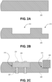
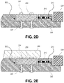
- FIG. 2A-2E a series of cross-sectional illustrations depicting a process for forming an electronic package with a glass substrate with embedded optical waveguides is shown, in accordance with an embodiment.
- the glass substrate 205 may have any suitable glass formulation.
- the glass substrate 205 may have a thickness between approximately 100 ⁇ m and approximately 5,000 ⁇ m.
- first recess 212 and the second recess 213 may be formed with any suitable material removal process, such as an etching process.
- a laser assisted etching process may be used to form the first recess 212 and the second recess 213.
- the first recess 212 is entirely within a perimeter of the glass substrate 205.
- the first recess 212 may have four sidewalls.
- the second recess 213 may be at an edge of the glass substrate 205.
- the second recess 213 may have fewer than four sidewalls (e.g., three sidewalls).
- the first recess 212 and the second recess 213 are shown as having the same depth into the glass substrate 205. However, in other embodiments, the depths of the first recess 212 and the second recess 213 may be non-uniform.
- the sidewalls of the first recess 212 and the second recess 213 are substantially vertical. In other embodiments, the sidewalls may be sloped so that the recesses have a taper.
- FIG. 2C a cross-sectional illustration of the glass substrate after the placement of the optics module 220 and the PIC 230 in the recesses 213 and 212 is shown, in accordance with an embodiment.
- the PIC 230 and the optics module 220 may be placed with a pick-and-place operation.
- through glass vias 207 may be formed through the glass substrate 205 below the first recess 212.
- the PIC 230 may be bonded to the through glass vias 207.
- a solder (not shown) may bond the PIC 230 to the through glass vias 207.
- the through glass vias 207 may be omitted in some embodiments.
- the PIC 230 may be secured to the glass substrate 205 by an adhesive or the like.
- Pads 231 may be provide over a top surface of the PIC 230.
- the pads 231 may be suitable for attaching to a die in a subsequent processing operation.
- the optics module 220 may be secured to the glass substrate 205 by an adhesive (not shown) or the like.
- the optical waveguide 210 is formed with a direct write operation. For example, a laser is scanned across the glass substrate 205 in order to change the structure of the glass at a desired depth within the glass substrate 205.
- the optical waveguide 210 may have a crystalline or partially crystalline microstructure while the surrounding glass substrate 205 has a substantially amorphous microstructure. The change in the microstructure may result in a change in the refractive index of the optical waveguide 210.
- the refractive index of the optical waveguide 210 may be higher than the refractive index of the glass substrate 205.
- the use of a direct write process to form the optical waveguides 210 is particularly beneficial. This is because the direct write process can account for any misalignment between the PIC 230 and the optics module 220. That is, if one or both of the PIC 230 and the optics module 220 are misaligned, the laser scan pattern can be easily modified to accommodate the misalignment.
- the die 240 may be any suitable die, such as a logic die, an FPGA, an SoC, or the like.
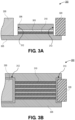
- FIGS. 3A and 3B illustrations of an electronic package 300 are shown, in accordance with an additional embodiment.
- the optical waveguides are provided between a pair of glass substrates.
- the electronic package 300 comprises a first glass substrate 305.
- An optical waveguide 310 may be provided over the first glass substrate 305.
- the optical waveguide 310 may be a material that has a higher refractive index than the first glass substrate 305.
- the optical waveguide 310 may comprise silicon and nitrogen (e.g., SiN x ).
- An adhesive 303 may be provided over the optical waveguide 310.
- a second glass substrate 306 may be attached to the structure by the adhesive 303.
- a first recess 312 and a second recess 313 are provided into the stack.
- the first recess 312 and the second recess 313 may extend entirely through the second glass substrate 306. In some embodiments the first recess 312 and the second recess 313 may also extend into the first glass substrate 305. In an embodiment, a PIC 330 may be provided in the first recess 312 and an optics module 320 may be provided in the second recess 313. The PIC 330 may be optically coupled to the optics module 320 by the optical waveguide 310.
- FIG. 3B a plan view illustration of the electronic package 300 is shown, in accordance with an embodiment.
- the second glass substrate 306 and the adhesive 303 are omitted for clarity.
- a plurality of optical waveguides 310 may be provided between the first recess 312 and the second recess 313.
- five optical waveguides 310 are shown.
- any number of optical waveguides 310 may be used.
- FIG. 4A-4I a series of cross-sectional illustrations depicting a process for forming an electronic package with embedded optical waveguides is shown, in accordance with an embodiment.
- the glass layer 405 may have any suitable glass formulation. Additionally, the glass layer 405 may have a thickness between approximately 100 ⁇ m and approximately 5,000 ⁇ m.
- the waveguide layer 411 may be a material that has a higher index of refraction than the glass layer 405.
- the waveguide layer 411 may comprise silicon and nitrogen (e.g., SiN x ).
- the waveguide layer 411 may be deposited with any suitable deposition process, (e.g., sputtering, chemical vapor deposition (CVD), physical vapor deposition (PVD), or the like).
- the mask 451 may have a pattern of the desired optical waveguides that are to be formed from the waveguide layer 411.
- the mask may be a hard mask or a soft mask.
- a hard mask may include a copper mask
- a soft mask may include a resist or the like.
- FIG. 4D a cross-sectional illustration of the glass layer 405 after the waveguide layer 411 is patterned is shown, in accordance with an embodiment.
- the mask 451 protects portions of the waveguide layer 411 during an etching process to form optical waveguides 410.
- the etching process may be a plasma etching process.
- FIG. 4E a cross-sectional illustration of the glass layer 405 after the mask 451 is removed is shown, in accordance with an embodiment.
- the mask 451 may be removed with an ashing process or other process selective to the mask 451 over the optical waveguides 410.
- the capping layer 403 may have an index of refraction that is lower than the index of refraction of the optical waveguides 410.
- the capping layer 403 may be an adhesive.
- a second glass layer (not shown) may be attached over the capping layer 403.
- the process of forming the optical waveguides may be complete.
- additional layers may be provided over the capping layer 403 in order to provide optical waveguides at multiple Z-heights, as shown in Figures 4G -41.
- the second waveguide layer 416 may be the same material as the optical waveguides 410.
- the second waveguide layer 416 may comprise silicon and nitrogen.
- the second waveguide layer 416 may be deposited with any suitable deposition process, such as sputtering.
- the second mask 452 may be a hardmask material or a soft mask material.
- the second mask 452 may be substantially similar to the mask 451 described in greater detail above.
- FIG. 41 a cross-sectional illustration of the glass layer 405 after the second waveguide layer 416 is patterned to form second optical waveguides 417 is shown, in accordance with an embodiment.
- the second optical waveguides 417 may be directly over the optical waveguides 410. Accordingly, it is to be appreciated that optical waveguides 410 and 417 may be provided at multiple Z-heights within a package substrate.
- an additional capping layer may be provided over the second optical waveguides 417.
- a second glass layer may then be provided over the second capping layer.
- additional layers of optical waveguides may be provided by repeating the process any number of times.
- FIG. 5A-5E a series of illustrations depicting a process for forming an electronic package is shown, in accordance with an embodiment.
- FIG. 5A a cross-sectional illustration of a glass layer 505 with optical waveguides 510 on a surface of the glass layer 505 is shown, in accordance with an embodiment.
- the optical waveguides 510 may be formed with a process similar to the process described above with respect to Figures 4A-4E , and will not be repeated here.
- the adhesive 503 has an index of refraction that is lower than the index of refraction of the optical waveguides 510.
- the second glass layer 506 may have a thickness that is substantially equal to a thickness of the glass layer 505. In other embodiment, the second glass layer 506 may have a thickness that is different than that of the glass layer 505.
- FIG. 5D a cross-sectional illustration of the glass layer 505 after the formation of a first recess 512 and a second recess 513 is shown, in accordance with an embodiment.
- the cross-section in Figure 5D is along the line 5-5' in Figure 5C . That is, the cross-section in Figure 5D is along the length of one of the optical waveguides 510.
- the first recess 512 and the second recess 513 extend through the second glass layer 506.
- the first recess 512 and the second recess 513 may also extend into the glass layer 505.
- the first recess 512 and the second recess 513 are substantially the same depth. In other embodiments, the first recess 512 and the second recess 513 may have different depths.
- FIG. 5E a cross-sectional illustration of the device after a PIC 530 and an optics module 520 are inserted in the recesses 512 and 513 is shown, in accordance with an embodiment.
- the PIC 530 is optically coupled to the optics module 520 by the optical waveguide 510.
- FIG. 6A-6I a series of illustrations depicting a process for forming an electronic package is shown, in accordance with an embodiment.
- improved control of the z-height alignment of the optical waveguide is provided compared to embodiments where the recess depth sets the z-height of the optical waveguide relative to optical components.
- the bottom glass layer is used as an etchstop for the recesses and a first layer is used to set the height of the optical waveguides. This provides improved control since thickness control of material deposition is more precise than depth control of an etching process.
- the glass layer 605 may be any suitable glass formulation.
- the glass layer 605 may have a thickness between approximately 100 ⁇ m and approximately 5,000 ⁇ m.
- the first layer 601 may be a material with a low index of refraction.
- the first layer 601 may comprise silicon and oxygen (e.g., SiO x ).
- the thickness of the first layer 601 may be precisely controlled in order to set the height of the optical waveguides above the glass layer 605.
- the waveguide layer 611 may be a material with an index of refraction that is greater than the index of refraction of the first layer 601.
- the waveguide layer 611 may comprise silicon and nitrogen (e.g., SiN x ).
- the waveguide layer 611 may be deposited with any suitable deposition process, such as sputtering.
- the mask layer 651 may be a hardmask material or a soft mask material.
- the mask layer 651 may have the pattern desired for the optical waveguides.
- optical waveguides 610 may be patterned with a plasma etching process or the like.
- FIG. 6F a cross-sectional illustration of the glass layer 605 after the mask layer 651 is removed is shown, in accordance with an embodiment.
- the mask layer 651 may be removed with an ashing process or other suitable material removal process that is selective to the material of the mask layer 651.
- the second layer 602 comprises an index of refraction that is lower than the index of refraction of the optical waveguides 610.
- the second layer 602 may be the same material as the first layer 601. Accordingly, the high index of refraction optical waveguides 610 are entirely surrounded by low index of refraction materials.
- the second glass layer 606 may be any glass formulation.
- the second glass layer 606 may be substantially similar to the glass layer 605.
- FIG. 61 a cross-sectional illustration of the structure after recesses 612 and 613 are formed is shown, in accordance with an embodiment.
- the cross-section in Figure 6I is along the line 6-6' in Figure 6H . That is, the cross-sectional illustration in Figure 6I is along the length of a single one of the optical waveguides 610.
- the first recess 612 and the second recess 613 extend through the second glass layer 606, the second layer 602, and the first layer 601.
- the glass layer 605 serves as a bottom etchstop for the recesses 612 and 613.
- the PIC 630 and the optics module 620 have a flat bottom surface on which they can be mounted. Additionally, the height of the optical waveguides 610 relative to the PIC 630 and the optics module 620 is precisely controlled by the height of the first layer 601.
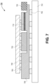
- the electronic system 790 comprises a board 791, such as a printed circuit board (PCB).
- a glass substrate 705 may be coupled to the board 791 by interconnects 792.
- a PIC 730 and an optics module 720 may be provided in recesses in the glass substrate 705.
- the PIC 730 may be optically coupled to the optics module 720 by an embedded optical waveguide 710.
- a die 740 may be coupled to the glass substrate 705 and PIC 730 by interconnects 793. While the glass substrate 705 and optical waveguide 710 similar to the structure in Figure 1A is shown in Figure 7 , it is to be appreciated that any of the optical waveguide architectures described herein may be used in the electronic system 790.
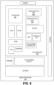
- FIG 8 illustrates a computing device 800 in accordance with one implementation of the invention.
- the computing device 800 houses a board 802.
- the board 802 may include a number of components, including but not limited to a processor 804 and at least one communication chip 806.
- the processor 804 is physically and electrically coupled to the board 802.
- the at least one communication chip 806 is also physically and electrically coupled to the board 802.
- the communication chip 806 is part of the processor 804.
- volatile memory e.g., DRAM
- nonvolatile memory e.g., ROM
- flash memory e.g., a graphics processor, a digital signal processor, a crypto processor, a chipset, an antenna, a display, a touchscreen display, a touchscreen controller, a battery, an audio codec, a video codec, a power amplifier, a global positioning system (GPS) device, a compass, an accelerometer, a gyroscope, a speaker, a camera, and a mass storage device (such as hard disk drive, compact disk (CD), digital versatile disk (DVD), and so forth).
- volatile memory e.g., DRAM
- nonvolatile memory e.g., ROM
- flash memory e.g., a graphics processor
- a digital signal processor e.g., a digital signal processor
- crypto processor e.g., a crypto processor
- chipset e.g., a chipset
- an antenna
- the communication chip 806 enables wireless communications for the transfer of data to and from the computing device 800.
- wireless and its derivatives may be used to describe circuits, devices, systems, methods, techniques, communications channels, etc., that may communicate data through the use of modulated electromagnetic radiation through a non-solid medium. The term does not imply that the associated devices do not contain any wires, although in some embodiments they might not.
- the communication chip 806 may implement any of a number of wireless standards or protocols, including but not limited to Wi-Fi (IEEE 802.11 family), WiMAX (IEEE 802.16 family), IEEE 802.20, long term evolution (LTE), Ev-DO, HSPA+, HSDPA+, HSUPA+, EDGE, GSM, GPRS, CDMA, TDMA, DECT, Bluetooth, derivatives thereof, as well as any other wireless protocols that are designated as 3G, 4G, 5G, and beyond.
- the computing device 800 may include a plurality of communication chips 806.
- a first communication chip 806 may be dedicated to shorter range wireless communications such as Wi-Fi and Bluetooth and a second communication chip 806 may be dedicated to longer range wireless communications such as GPS, EDGE, GPRS, CDMA, WiMAX, LTE, Ev-DO, and others.
- the processor 804 of the computing device 800 includes an integrated circuit die packaged within the processor 804.
- the integrated circuit die of the processor may be part of an electronic package that comprises a glass substrate with an embedded optical waveguide, in accordance with embodiments described herein.
- the term "processor" may refer to any device or portion of a device that processes electronic data from registers and/or memory to transform that electronic data into other electronic data that may be stored in registers and/or memory.
- the communication chip 806 also includes an integrated circuit die packaged within the communication chip 806.
- the integrated circuit die of the communication chip may be part of an electronic package that comprises a glass substrate with an embedded optical waveguide, in accordance with embodiments described herein.
Landscapes
- Physics & Mathematics (AREA)
- Engineering & Computer Science (AREA)
- Microelectronics & Electronic Packaging (AREA)
- General Physics & Mathematics (AREA)
- Optics & Photonics (AREA)
- Optical Integrated Circuits (AREA)
Abstract
Description
- Embodiments of the present disclosure relate to electronic packages, and more particularly to glass substrates with embedded waveguides for photonics connections.
- Next generation server high speed communication protocols are expected to rely heavily on optical interconnect architectures. As such, high-density interconnect substrate packages need to accommodate multiple photonic devices. Currently, bridge architectures (e.g., embedded multi-die interconnect bridge (EMIB) architectures) are used to support multi-chip packaging with photonic devices connected to the silicon logic die through the bridge die. In this configuration, fiber bundles are attached to the photonic IC from the side (e.g., with a V-groove connection or a multi-lens array).
- Assembly of these fiber bundles is non-trivial due to the stringent alignment requirement which is exacerbated by the undulation and warpage of standard organic substrate packages. One proposal is to use glass cored substrates to provide a flatter, more rigid starting material. However, the addition of organic layers and plating steps can increase the final undulation and warpage that the photonic components see.
-
-
Figure 1A is a cross-sectional illustration of an electronic package with a glass substrate with an embedded optical waveguide between an optics module and a photonics integrated circuit (PIC), in accordance with an embodiment. -
Figure 1B is a cross-sectional illustration of an electronic package with a glass substrate with embedded optical waveguides between PICs and between an optics module and one of the PICs, in accordance with an embodiment. -
Figures 2A-2E are cross-sectional illustrations depicting a process to form an electronic package with a glass substrate and an embedded optical waveguide, in accordance with an embodiment. -
Figure 3A is a cross-sectional illustration of an electronic package with a first glass substrate, a second glass substrate, and an optical waveguide positioned between the first glass substrate and the second glass substrate, in accordance with an embodiment. -
Figure 3B is a plan view illustration of an electronic package with a plurality of optical waveguides between a PIC and an optics module, in accordance with an embodiment. -
Figures 4A-4I are cross-sectional illustrations depicting a process for forming an electronic package with optical waveguides embedded in a glass substrate, in accordance with an embodiment. -
Figures 5A-5E are cross-sectional illustrations depicting a process for forming an electronic package with optical waveguides embedded in a glass substrate, in accordance with an embodiment. -
Figures 6A-6I are cross-sectional illustrations depicting a process for forming an electronic package with optical waveguides embedded between two low refractive index layers, in accordance with an embodiment. -
Figure 7 is a cross-sectional illustration of the electronic system with a glass substrate with embedded optical waveguides, in accordance with an embodiment. -
Figure 8 is a schematic of a computing device built in accordance with an embodiment. - Described herein are electronic packages with glass substrates with embedded waveguides for photonics connections, in accordance with various embodiments. In the following description, various aspects of the illustrative implementations will be described using terms commonly employed by those skilled in the art to convey the substance of their work to others skilled in the art. However, it will be apparent to those skilled in the art that the present invention may be practiced with only some of the described aspects. For purposes of explanation, specific numbers, materials and configurations are set forth in order to provide a thorough understanding of the illustrative implementations. However, it will be apparent to one skilled in the art that the present invention may be practiced without the specific details. In other instances, well-known features are omitted or simplified in order not to obscure the illustrative implementations.
- Various operations will be described as multiple discrete operations, in turn, in a manner that is most helpful in understanding the present invention, however, the order of description should not be construed to imply that these operations are necessarily order dependent. In particular, these operations need not be performed in the order of presentation.
- As noted above, optical interconnect architectures are needed for high speed communication protocols for next generation server products. Existing architectures for enabling optical interconnects are limited. Particularly, the warpage and deformation present in organic packaging architectures makes the alignment and attachment of optical interconnects in the package difficult and low yielding.
- Accordingly, embodiments disclosed herein include package substrates that are glass. The glass substrates may improve planarity and reduce warpage. In some embodiments, the optical interconnects are made before any organic layers are provided over the glass substrate. In some embodiments, optical components (e.g., photonics integrated circuits (PICs), optics modules (e.g., lenses, etc.) may be placed in recesses into the glass substrate. Optical connections between the optical components may be made by embedded optical waveguides. In some embodiments, the optical waveguides are formed with a direct write process. In a direct write process a laser is scanned over portions of the glass substrate where an optical waveguide is needed. The laser can produce a change in the microstructure of the glass that provides an increase in the refractive index. In other embodiments, the optical waveguides are formed with a lithographic patterning process. A second glass substrate may then be adhered to the underlying glass substrate so that the optical waveguides are between the pair of glass substrates.
- Referring now to
Figure 1A , a cross-sectional illustration of anelectronic package 100 is shown, in accordance with an embodiment. In an embodiment, theelectronic package 100 comprises aglass substrate 105. Theglass substrate 105 may have any glass formulation. The use of aglass substrate 105 improves the rigidity and planarity of theelectronic package 100. As such, it is easier to integrate optical components with proper alignment. Theglass substrate 105 may have a thickness between approximately 100µm and approximately 5,000µm. Though, it is to be appreciated that thinner orthicker glass substrates 105 may also be used. - In an embodiment, recesses may be formed into the top surface of the
glass substrate 105. InFigure 1A , afirst recess 112 and asecond recess 113 are provided into theglass substrate 105. In the illustrated embodiment, the depths of thefirst recess 112 and thesecond recess 113 are substantially equal. However, in other embodiments, thefirst recess 112 and thesecond recess 113 may have different depths. In an embodiment, thefirst recess 112 is towards a middle of theglass substrate 105, and thesecond recess 113 is at an edge of theglass substrate 105. In an embodiment, throughglass vias 107 may be provided below thefirst recess 113. Through glass vias (not shown) may also be provided from the top surface of theglass substrate 105 to the bottom surface of theglass substrate 105. - In an embodiment, photonics components may be placed into the
first recess 112 and thesecond recess 113. For example, anoptics module 120 may be placed in thesecond recess 113. Theoptics module 120 may include optics features to couple the electronic package to external optical fibers (not shown). For example, theoptics module 120 may comprise lenses, optical fibers, mechanical features for aligning fibers, and the like. In an embodiment, aPIC 130 may be placed in thefirst recess 112. ThePIC 130 has circuitry and functionality to convert signals between an optical regime and an electrical regime. The electrical side of thePIC 130 may be connected to a die 140 byinterconnects 131. The die 140 may be a logic die, an FPGA, an SoC, or the like. Thedie 140 may be provided over a top surface of theglass substrate 105. - In an embodiment, the
optics module 120 is optically coupled to thePIC 130 by an embeddedoptical waveguide 110. Theoptical waveguide 110 may be entirely embedded in theglass substrate 105. That is, theglass substrate 105 surrounds and entire perimeter of theoptical waveguide 110. Theoptical waveguide 110 may be substantially the same material as theglass substrate 105. However, theoptical waveguide 110 has been treated in order to change the refractive index to be higher than the surroundingglass substrate 105. For example, a laser treatment of portions of theglass substrate 105 may result in the microstructure of theoptical waveguide 110 being different than a microstructure of theglass substrate 105. In some embodiments, theoptical waveguide 110 may have a substantially crystalline microstructure or partially crystalline microstructure, and theglass substrate 105 may have a substantially amorphous microstructure. In an embodiment, theoptical waveguide 110 may extend from a sidewall of thefirst recess 112 to a sidewall of thesecond recess 113. - Additionally, while a single
optical waveguide 110 is shown, it is to be appreciated that a plurality ofoptical waveguides 110 may optically couple theoptics module 120 to thePIC 130. In some embodiments, each of the plurality ofoptical waveguides 110 are at the same z-height in theglass substrate 105. In other embodiments, theoptical waveguides 110 may be a different z-heights in theglass substrate 105. - Referring now to
Figure 1B , a cross-sectional illustration of anelectronic package 100 is shown, in accordance with an additional embodiment. In an embodiment, theelectronic package 100 inFigure 1B may be substantially similar to theelectronic package 100 inFigure 1A , with the exception of there being a pair offirst recesses PICs first PIC 130A may be placed in thefirst recess 112A and thesecond PIC 130B may be placed in thefirst recess 112B. Additionally, a through glass via 108 from the top surface of theglass substrate 105 to a bottom surface of theglass substrate 105 is shown. - In an embodiment, the
first PIC 130A may be optically coupled to thesecond PIC 130B by a secondoptical waveguide 110B. In an embodiment, the secondoptical waveguide 110B may be at the same z-height within theglass substrate 105 as the firstoptical waveguide 110A between thefirst PIC 130A and theoptics module 120. In other embodiments, the secondoptical waveguide 110B and the firstoptical waveguide 110A may be different z-heights. The secondoptical waveguide 110B may be substantially similar to the firstoptical waveguide 110A. For example, the secondoptical waveguide 110B may have a crystalline or partially crystalline microstructure that provides a higher refractive index than the surroundingglass substrate 105. - Referring now to
Figure 2A-2E , a series of cross-sectional illustrations depicting a process for forming an electronic package with a glass substrate with embedded optical waveguides is shown, in accordance with an embodiment. - Referring now to
Figure 2A , a cross-sectional illustration of theglass substrate 205 is shown, in accordance with an embodiment. In an embodiment, theglass substrate 205 may have any suitable glass formulation. Theglass substrate 205 may have a thickness between approximately 100µm and approximately 5,000µm. - Referring now to
Figure 2B , a cross-sectional illustration of theglass substrate 205 after afirst recess 212 and asecond recess 213 are formed into theglass substrate 205 is shown, in accordance with an embodiment. In an embodiment, thefirst recess 212 and thesecond recess 213 may be formed with any suitable material removal process, such as an etching process. In a particular embodiment, a laser assisted etching process may be used to form thefirst recess 212 and thesecond recess 213. - In an embodiment, the
first recess 212 is entirely within a perimeter of theglass substrate 205. As such, thefirst recess 212 may have four sidewalls. Thesecond recess 213 may be at an edge of theglass substrate 205. As such, thesecond recess 213 may have fewer than four sidewalls (e.g., three sidewalls). In the illustrated embodiment, thefirst recess 212 and thesecond recess 213 are shown as having the same depth into theglass substrate 205. However, in other embodiments, the depths of thefirst recess 212 and thesecond recess 213 may be non-uniform. In the illustrated embodiment, the sidewalls of thefirst recess 212 and thesecond recess 213 are substantially vertical. In other embodiments, the sidewalls may be sloped so that the recesses have a taper. - Referring now to
Figure 2C , a cross-sectional illustration of the glass substrate after the placement of theoptics module 220 and thePIC 230 in therecesses PIC 230 and theoptics module 220 may be placed with a pick-and-place operation. In some embodiments, throughglass vias 207 may be formed through theglass substrate 205 below thefirst recess 212. ThePIC 230 may be bonded to the throughglass vias 207. For example, a solder (not shown) may bond thePIC 230 to the throughglass vias 207. However, it is to be appreciated that the throughglass vias 207 may be omitted in some embodiments. In such embodiments, thePIC 230 may be secured to theglass substrate 205 by an adhesive or the like.Pads 231 may be provide over a top surface of thePIC 230. Thepads 231 may be suitable for attaching to a die in a subsequent processing operation. In an embodiment, theoptics module 220 may be secured to theglass substrate 205 by an adhesive (not shown) or the like. - Referring now to
Figure 2D , a cross-sectional illustration of theglass substrate 205 after formation of anoptical waveguide 210 is shown, in accordance with an embodiment. In an embodiment, theoptical waveguide 210 is formed with a direct write operation. For example, a laser is scanned across theglass substrate 205 in order to change the structure of the glass at a desired depth within theglass substrate 205. For example, theoptical waveguide 210 may have a crystalline or partially crystalline microstructure while the surroundingglass substrate 205 has a substantially amorphous microstructure. The change in the microstructure may result in a change in the refractive index of theoptical waveguide 210. Particularly, the refractive index of theoptical waveguide 210 may be higher than the refractive index of theglass substrate 205. - The use of a direct write process to form the
optical waveguides 210 is particularly beneficial. This is because the direct write process can account for any misalignment between thePIC 230 and theoptics module 220. That is, if one or both of thePIC 230 and theoptics module 220 are misaligned, the laser scan pattern can be easily modified to accommodate the misalignment. - Referring now to
Figure 2E , a cross-sectional illustration of theglass substrate 205 after adie 240 is attached to thePIC 230 is shown, in accordance with an embodiment. In an embodiment, thedie 240 may be any suitable die, such as a logic die, an FPGA, an SoC, or the like. - Referring now to
Figures 3A and 3B , illustrations of anelectronic package 300 are shown, in accordance with an additional embodiment. Instead of an optical waveguide that is embedded in a glass substrate, the optical waveguides are provided between a pair of glass substrates. - Referring now to
Figure 3A , a cross-sectional illustration of anelectronic package 300 is shown, in accordance with an embodiment. In an embodiment, theelectronic package 300 comprises afirst glass substrate 305. Anoptical waveguide 310 may be provided over thefirst glass substrate 305. Theoptical waveguide 310 may be a material that has a higher refractive index than thefirst glass substrate 305. For example, theoptical waveguide 310 may comprise silicon and nitrogen (e.g., SiNx). An adhesive 303 may be provided over theoptical waveguide 310. Asecond glass substrate 306 may be attached to the structure by the adhesive 303. In an embodiment, afirst recess 312 and asecond recess 313 are provided into the stack. Thefirst recess 312 and thesecond recess 313 may extend entirely through thesecond glass substrate 306. In some embodiments thefirst recess 312 and thesecond recess 313 may also extend into thefirst glass substrate 305. In an embodiment, aPIC 330 may be provided in thefirst recess 312 and anoptics module 320 may be provided in thesecond recess 313. ThePIC 330 may be optically coupled to theoptics module 320 by theoptical waveguide 310. - Referring now to
Figure 3B , a plan view illustration of theelectronic package 300 is shown, in accordance with an embodiment. InFigure 3B thesecond glass substrate 306 and the adhesive 303 are omitted for clarity. As shown, a plurality ofoptical waveguides 310 may be provided between thefirst recess 312 and thesecond recess 313. For example fiveoptical waveguides 310 are shown. However, it is to be appreciated that any number ofoptical waveguides 310 may be used. - Referring now to
Figures 4A-4I , a series of cross-sectional illustrations depicting a process for forming an electronic package with embedded optical waveguides is shown, in accordance with an embodiment. - Referring now to
Figure 4A , a cross-sectional illustration of aglass layer 405 is shown, in accordance with an embodiment. Theglass layer 405 may have any suitable glass formulation. Additionally, theglass layer 405 may have a thickness between approximately 100µm and approximately 5,000µm. - Referring now to
Figure 4B , a cross-sectional illustration of theglass layer 405 after awaveguide layer 411 is deposited over theglass layer 405 is shown, in accordance with an embodiment. In an embodiment, thewaveguide layer 411 may be a material that has a higher index of refraction than theglass layer 405. For example, thewaveguide layer 411 may comprise silicon and nitrogen (e.g., SiNx). Thewaveguide layer 411 may be deposited with any suitable deposition process, (e.g., sputtering, chemical vapor deposition (CVD), physical vapor deposition (PVD), or the like). - Referring now to
Figure 4C , a cross-sectional illustration of theglass layer 405 after amask 451 is disposed over thewaveguide layer 411 is shown, in accordance with an embodiment. In an embodiment, themask 451 may have a pattern of the desired optical waveguides that are to be formed from thewaveguide layer 411. In an embodiment, the mask may be a hard mask or a soft mask. For example, a hard mask may include a copper mask, and a soft mask may include a resist or the like. - Referring now to
Figure 4D , a cross-sectional illustration of theglass layer 405 after thewaveguide layer 411 is patterned is shown, in accordance with an embodiment. As shown, themask 451 protects portions of thewaveguide layer 411 during an etching process to formoptical waveguides 410. In an embodiment, the etching process may be a plasma etching process. - Referring now to
Figure 4E , a cross-sectional illustration of theglass layer 405 after themask 451 is removed is shown, in accordance with an embodiment. Themask 451 may be removed with an ashing process or other process selective to themask 451 over theoptical waveguides 410. - Referring now to
Figure 4F , a cross-sectional illustration of theglass layer 405 after acapping layer 403 is disposed over theglass layer 405 and theoptical waveguides 410 is shown, in accordance with an embodiment. In an embodiment, thecapping layer 403 may have an index of refraction that is lower than the index of refraction of theoptical waveguides 410. In some embodiments, thecapping layer 403 may be an adhesive. When thecapping layer 403 is an adhesive, a second glass layer (not shown) may be attached over thecapping layer 403. When a second glass layer is attached, the process of forming the optical waveguides may be complete. However, in other embodiments, additional layers may be provided over thecapping layer 403 in order to provide optical waveguides at multiple Z-heights, as shown inFigures 4G -41. - Referring now to
Figure 4G , a cross-sectional illustration of theglass layer 405 after asecond waveguide layer 416 is deposited over thecapping layer 403 is shown, in accordance with an embodiment. Thesecond waveguide layer 416 may be the same material as theoptical waveguides 410. For example, thesecond waveguide layer 416 may comprise silicon and nitrogen. Thesecond waveguide layer 416 may be deposited with any suitable deposition process, such as sputtering. - Referring now to
Figure 4H , a cross-sectional illustration of theglass layer 405 after asecond mask 452 is formed over thesecond waveguide layer 416 is shown, in accordance with an embodiment. Thesecond mask 452 may be a hardmask material or a soft mask material. Thesecond mask 452 may be substantially similar to themask 451 described in greater detail above. - Referring now to Figure 41, a cross-sectional illustration of the
glass layer 405 after thesecond waveguide layer 416 is patterned to form secondoptical waveguides 417 is shown, in accordance with an embodiment. As shown, the secondoptical waveguides 417 may be directly over theoptical waveguides 410. Accordingly, it is to be appreciated thatoptical waveguides - After formation of the second
optical waveguides 417, an additional capping layer (not shown) may be provided over the secondoptical waveguides 417. A second glass layer (not shown) may then be provided over the second capping layer. In other embodiments, additional layers of optical waveguides may be provided by repeating the process any number of times. - Referring now to
Figures 5A-5E , a series of illustrations depicting a process for forming an electronic package is shown, in accordance with an embodiment. - Referring now to
Figure 5A , a cross-sectional illustration of aglass layer 505 withoptical waveguides 510 on a surface of theglass layer 505 is shown, in accordance with an embodiment. In an embodiment, theoptical waveguides 510 may be formed with a process similar to the process described above with respect toFigures 4A-4E , and will not be repeated here. - Referring now to
Figure 5B , a cross-sectional illustration of theglass layer 505 after an adhesive 503 is provided over theoptical waveguides 510 and theglass layer 505 is shown, in accordance with an embodiment. In an embodiment, the adhesive 503 has an index of refraction that is lower than the index of refraction of theoptical waveguides 510. - Referring now to
Figure 5C , a cross-sectional illustration of theglass layer 505 after asecond glass layer 506 is disposed over the adhesive 503 is shown, in accordance with an embodiment. In an embodiment, thesecond glass layer 506 may have a thickness that is substantially equal to a thickness of theglass layer 505. In other embodiment, thesecond glass layer 506 may have a thickness that is different than that of theglass layer 505. - Referring now to
Figure 5D , a cross-sectional illustration of theglass layer 505 after the formation of afirst recess 512 and asecond recess 513 is shown, in accordance with an embodiment. The cross-section inFigure 5D is along the line 5-5' inFigure 5C . That is, the cross-section inFigure 5D is along the length of one of theoptical waveguides 510. As shown, thefirst recess 512 and thesecond recess 513 extend through thesecond glass layer 506. Thefirst recess 512 and thesecond recess 513 may also extend into theglass layer 505. In the illustrated embodiment, thefirst recess 512 and thesecond recess 513 are substantially the same depth. In other embodiments, thefirst recess 512 and thesecond recess 513 may have different depths. - Referring now to
Figure 5E , a cross-sectional illustration of the device after aPIC 530 and anoptics module 520 are inserted in therecesses PIC 530 is optically coupled to theoptics module 520 by theoptical waveguide 510. - Referring now to
Figures 6A-6I , a series of illustrations depicting a process for forming an electronic package is shown, in accordance with an embodiment. In the embodiment shown inFigures 6A-6I , improved control of the z-height alignment of the optical waveguide is provided compared to embodiments where the recess depth sets the z-height of the optical waveguide relative to optical components. Instead, the bottom glass layer is used as an etchstop for the recesses and a first layer is used to set the height of the optical waveguides. This provides improved control since thickness control of material deposition is more precise than depth control of an etching process. - Referring now to
Figure 6A , a cross-sectional illustration of aglass layer 605 is shown, in accordance with an embodiment. Theglass layer 605 may be any suitable glass formulation. Theglass layer 605 may have a thickness between approximately 100µm and approximately 5,000µm. - Referring now to
Figure 6B , a cross-sectional illustration of theglass layer 605 after afirst layer 601 is disposed over theglass layer 605 is shown, in accordance with an embodiment. Thefirst layer 601 may be a material with a low index of refraction. In a particular embodiment, thefirst layer 601 may comprise silicon and oxygen (e.g., SiOx). The thickness of thefirst layer 601 may be precisely controlled in order to set the height of the optical waveguides above theglass layer 605. - Referring now to
Figure 6C , a cross-sectional illustration of theglass layer 605 after awaveguide layer 611 is disposed over thefirst layer 601 is shown, in accordance with an embodiment. Thewaveguide layer 611 may be a material with an index of refraction that is greater than the index of refraction of thefirst layer 601. For example, thewaveguide layer 611 may comprise silicon and nitrogen (e.g., SiNx). Thewaveguide layer 611 may be deposited with any suitable deposition process, such as sputtering. - Referring no to
Figure 6D , a cross-sectional illustration of theglass layer 605 after amask layer 651 is provided over thewaveguide layer 611 is shown, in accordance with an embodiment. In an embodiment, themask layer 651 may be a hardmask material or a soft mask material. Themask layer 651 may have the pattern desired for the optical waveguides. - Referring now to
Figure 6E , a cross-sectional illustration of theglass layer 605 after thewaveguide layer 611 is patterned to formoptical waveguides 610 is shown, in accordance with an embodiment. In an embodiment, theoptical waveguides 610 may be patterned with a plasma etching process or the like. - Referring now to
Figure 6F , a cross-sectional illustration of theglass layer 605 after themask layer 651 is removed is shown, in accordance with an embodiment. Themask layer 651 may be removed with an ashing process or other suitable material removal process that is selective to the material of themask layer 651. - Referring now to
Figure 6G , a cross-sectional illustration of theglass layer 605 after asecond layer 602 is provided over thefirst layer 601 and theoptical waveguides 610 is shown, in accordance with an embodiment. In an embodiment, thesecond layer 602 comprises an index of refraction that is lower than the index of refraction of theoptical waveguides 610. In some embodiments, thesecond layer 602 may be the same material as thefirst layer 601. Accordingly, the high index of refractionoptical waveguides 610 are entirely surrounded by low index of refraction materials. - Referring now to
Figure 6H , a cross-sectional illustration of theglass layer 605 after asecond glass layer 606 is provided over thesecond layer 602 is shown, in accordance with an embodiment. In an embodiment, thesecond glass layer 606 may be any glass formulation. In an embodiment, thesecond glass layer 606 may be substantially similar to theglass layer 605. - Referring now to Figure 61, a cross-sectional illustration of the structure after
recesses Figure 6I is along the line 6-6' inFigure 6H . That is, the cross-sectional illustration inFigure 6I is along the length of a single one of theoptical waveguides 610. As shown, thefirst recess 612 and thesecond recess 613 extend through thesecond glass layer 606, thesecond layer 602, and thefirst layer 601. Theglass layer 605 serves as a bottom etchstop for therecesses PIC 630 and theoptics module 620 have a flat bottom surface on which they can be mounted. Additionally, the height of theoptical waveguides 610 relative to thePIC 630 and theoptics module 620 is precisely controlled by the height of thefirst layer 601. - Referring now to
Figure 7 , anelectronic system 790 is shown, in accordance with an embodiment. In an embodiment, theelectronic system 790 comprises aboard 791, such as a printed circuit board (PCB). Aglass substrate 705 may be coupled to theboard 791 byinterconnects 792. In an embodiment, aPIC 730 and anoptics module 720 may be provided in recesses in theglass substrate 705. In an embodiment, thePIC 730 may be optically coupled to theoptics module 720 by an embeddedoptical waveguide 710. Adie 740 may be coupled to theglass substrate 705 andPIC 730 byinterconnects 793. While theglass substrate 705 andoptical waveguide 710 similar to the structure inFigure 1A is shown inFigure 7 , it is to be appreciated that any of the optical waveguide architectures described herein may be used in theelectronic system 790. -
Figure 8 illustrates acomputing device 800 in accordance with one implementation of the invention. Thecomputing device 800 houses aboard 802. Theboard 802 may include a number of components, including but not limited to aprocessor 804 and at least onecommunication chip 806. Theprocessor 804 is physically and electrically coupled to theboard 802. In some implementations the at least onecommunication chip 806 is also physically and electrically coupled to theboard 802. In further implementations, thecommunication chip 806 is part of theprocessor 804. - These other components include, but are not limited to, volatile memory (e.g., DRAM), nonvolatile memory (e.g., ROM), flash memory, a graphics processor, a digital signal processor, a crypto processor, a chipset, an antenna, a display, a touchscreen display, a touchscreen controller, a battery, an audio codec, a video codec, a power amplifier, a global positioning system (GPS) device, a compass, an accelerometer, a gyroscope, a speaker, a camera, and a mass storage device (such as hard disk drive, compact disk (CD), digital versatile disk (DVD), and so forth).
- The
communication chip 806 enables wireless communications for the transfer of data to and from thecomputing device 800. The term "wireless" and its derivatives may be used to describe circuits, devices, systems, methods, techniques, communications channels, etc., that may communicate data through the use of modulated electromagnetic radiation through a non-solid medium. The term does not imply that the associated devices do not contain any wires, although in some embodiments they might not. Thecommunication chip 806 may implement any of a number of wireless standards or protocols, including but not limited to Wi-Fi (IEEE 802.11 family), WiMAX (IEEE 802.16 family), IEEE 802.20, long term evolution (LTE), Ev-DO, HSPA+, HSDPA+, HSUPA+, EDGE, GSM, GPRS, CDMA, TDMA, DECT, Bluetooth, derivatives thereof, as well as any other wireless protocols that are designated as 3G, 4G, 5G, and beyond. Thecomputing device 800 may include a plurality ofcommunication chips 806. For instance, afirst communication chip 806 may be dedicated to shorter range wireless communications such as Wi-Fi and Bluetooth and asecond communication chip 806 may be dedicated to longer range wireless communications such as GPS, EDGE, GPRS, CDMA, WiMAX, LTE, Ev-DO, and others. - The
processor 804 of thecomputing device 800 includes an integrated circuit die packaged within theprocessor 804. In some implementations of the invention, the integrated circuit die of the processor may be part of an electronic package that comprises a glass substrate with an embedded optical waveguide, in accordance with embodiments described herein. The term "processor" may refer to any device or portion of a device that processes electronic data from registers and/or memory to transform that electronic data into other electronic data that may be stored in registers and/or memory. - The
communication chip 806 also includes an integrated circuit die packaged within thecommunication chip 806. In accordance with another implementation of the invention, the integrated circuit die of the communication chip may be part of an electronic package that comprises a glass substrate with an embedded optical waveguide, in accordance with embodiments described herein. - The above description of illustrated implementations of the invention, including what is described in the Abstract, is not intended to be exhaustive or to limit the invention to the precise forms disclosed. While specific implementations of, and examples for, the invention are described herein for illustrative purposes, various equivalent modifications are possible within the scope of the invention, as those skilled in the relevant art will recognize.
- These modifications may be made to the invention in light of the above detailed description. The terms used in the following claims should not be construed to limit the invention to the specific implementations disclosed in the specification and the claims. Rather, the scope of the invention is to be determined entirely by the following claims, which are to be construed in accordance with established doctrines of claim interpretation.
- Example 1: an electronic package, comprising: a first glass substrate; an adhesive over the first glass substrate; a second glass substrate over the adhesive; and an optical waveguide embedded in the adhesive.
- Example 2: the electronic package of Example 1, further comprising: a first recess through the second glass substrate and the adhesive; a second recess through the second glass substrate and the adhesive; a photonics integrated circuit (PIC) in the first recess; and an optics module in the second recess, wherein the optical waveguide optically couples the PIC to the optics module.
- Example 3: the electronic package of Example 2, wherein the first recess and the second recess extend into the first glass substrate.
- Example 4: the electronic package of Example 2 or Example 3, wherein the optics module comprises a lens for coupling with an optical fiber.
- Example 5: the electronic package of Examples 1-4, wherein the adhesive comprises: a first layer with a first refractive index, wherein the first layer is between the first glass substrate and the optical waveguide; and a second layer with the first refractive index, wherein the second layer is over and around the optical waveguide, and wherein the optical waveguide has a second refractive index that is higher than the first refractive index.
- Example 6: the electronic package of Example 5, wherein the first layer and the second layer comprise silicon and oxygen, and wherein the optical waveguide comprises silicon and nitrogen.
- Example 7: the electronic package of Example 5 or Example 6, wherein the first layer has a first thickness and the second layer has a second thickness, and wherein the first thickness is greater than the second thickness.
- Example 8: the electronic package of Examples 1-7, wherein a surface of the optical waveguide is in contact with a surface of the first glass layer.
- Example 9: the electronic package of Example 7, wherein the adhesive is over and around the optical waveguide.
- Example 10: the electronic package of Examples 7-9, further comprising: a second optical waveguide over the adhesive, wherein the second optical waveguide is positioned directly above the optical waveguide.
- Example 11: an electronic package, comprising: a glass substrate with a first recess and a second recess; a photonics integrated circuit (PIC) in the first recess; an optics module in the second recess; and an optical waveguide embedded in the glass substrate between the first recess and the second recess, wherein the optical waveguide optically couples the PIC to the optics module.
- Example 12: the electronic package of Example 11, wherein the optical waveguide comprises the same material as the glass substrate, and wherein a microstructure of the optical waveguide is different than a microstructure of the glass substrate.
- Example 13: the electronic package of Example 11 or Example 12, further comprising: a third recess in the glass substrate; a second PIC in the third recess; and a second optical waveguide embedded in the glass between the first recess and the third recess, wherein the second optical waveguide optically couples the PIC to the second PIC.
- Example 14: the electronic package of Examples 11-13, wherein the optics module comprises a lens for coupling to an optical fiber.
- Example 15: the electronic package of Examples 11-14, further comprising: a through glass via below the first recess, wherein the through glass via is electrically coupled to the PIC.
- Example 16: the electronic package of Examples 11-14, further comprising: a through glass via adjacent to the first recess, wherein the through glass via extends between a first surface of the glass substrate and a second surface of the glass substrate.
- Example 17: the electronic package of Examples 11-16, wherein the first recess has a first depth and the second recess has a second depth.
- Example 18: the electronic package of Example 17, wherein the first depth is substantially equal to the second depth.
- Example 19: a method of forming a package substrate, comprising: depositing a first layer over a first glass substrate; patterning the first layer to form a plurality of optical waveguides; disposing an adhesive over the first glass substrate and the optical waveguides; and attaching a second glass substrate to the adhesive.
- Example 20: the method of Example 19, wherein the optical waveguides have a first index of refraction, and wherein the adhesive has a second index of refraction that is lower than the first index of refraction.
- Example 21: the method of Example 19 or Example 20, further comprising: forming a first recess into the second glass substrate and the adhesive; and forming a second recess into the second glass substrate and the adhesive.
- Example 22: the method of Example 21, wherein a photonics integrated circuit (PIC) is placed into the first recess and an optics module is placed into the second recess, and wherein the optical waveguides optically couple the PIC to the optics module.
- Example 23: an electronic system, comprising: a board; a package substrate coupled to the board, wherein the package substrate comprises: a first glass substrate; an adhesive over the first glass substrate; a second glass substrate over the adhesive; an optical waveguide embedded in the adhesive; a first recess through the second glass substrate and the adhesive; a second recess through the second glass substrate and the adhesive; a photonics integrated circuit (PIC) in the first recess; and an optics module in the second recess, wherein the optical waveguide optically couples the PIC to the optics module; and a die coupled to the package substrate.
- Example 24: the electronic package of Example 23, wherein the first recess and the second recess extend into the first glass substrate.
- Example 25: the electronic package of Example 23 or Example 24, wherein the adhesive comprises: a first layer with a first refractive index, wherein the first layer is between the first glass substrate and the optical waveguide; and a second layer with the first refractive index, wherein the second layer is over and around the optical waveguide, and wherein the optical waveguide has a second refractive index that is higher than the first refractive index.
Claims (14)
- An electronic package, comprising:a first glass substrate;an adhesive over the first glass substrate;a second glass substrate over the adhesive; andan optical waveguide embedded in the adhesive.
- The electronic package of claim 1, further comprising:a first recess through the second glass substrate and the adhesive;a second recess through the second glass substrate and the adhesive;a photonics integrated circuit (PIC) in the first recess; andan optics module in the second recess, wherein the optical waveguide optically couples the PIC to the optics module.
- The electronic package of claim 2, wherein the first recess and the second recess extend into the first glass substrate.
- The electronic package of claim 2 or 3, wherein the optics module comprises a lens for coupling with an optical fiber.
- The electronic package of claim 1, 2, 3 or 4, wherein the adhesive comprises:a first layer with a first refractive index, wherein the first layer is between the first glass substrate and the optical waveguide; anda second layer with the first refractive index, wherein the second layer is over and around the optical waveguide, and wherein the optical waveguide has a second refractive index that is higher than the first refractive index.
- The electronic package of claim 5, wherein the first layer and the second layer comprise silicon and oxygen, and wherein the optical waveguide comprises silicon and nitrogen.
- The electronic package of claim 5 or 6, wherein the first layer has a first thickness and the second layer has a second thickness, and wherein the first thickness is greater than the second thickness.
- The electronic package of claim 1, 2, 3, 4, 5, 6 or 7, wherein a surface of the optical waveguide is in contact with a surface of the first glass layer.
- The electronic package of claim 7, wherein the adhesive is over and around the optical waveguide.
- The electronic package of claim 7, 8 or 9, further comprising:
a second optical waveguide over the adhesive, wherein the second optical waveguide is positioned directly above the optical waveguide. - A method of forming a package substrate, comprising:depositing a first layer over a first glass substrate;patterning the first layer to form a plurality of optical waveguides;disposing an adhesive over the first glass substrate and the optical waveguides; andattaching a second glass substrate to the adhesive.
- The method of claim 11, wherein the optical waveguides have a first index of refraction, and wherein the adhesive has a second index of refraction that is lower than the first index of refraction.
- The method of claim 11 or 12, further comprising:forming a first recess into the second glass substrate and the adhesive; andforming a second recess into the second glass substrate and the adhesive.
- The method of claim 13, wherein a photonics integrated circuit (PIC) is placed into the first recess and an optics module is placed into the second recess, and wherein the optical waveguides optically couple the PIC to the optics module.
Applications Claiming Priority (1)
| Application Number | Priority Date | Filing Date | Title |
|---|---|---|---|
| US17/476,357 US12504581B2 (en) | 2021-09-15 | 2021-09-15 | Photonic interconnect and components in glass |
Publications (2)
| Publication Number | Publication Date |
|---|---|
| EP4152060A1 true EP4152060A1 (en) | 2023-03-22 |
| EP4152060B1 EP4152060B1 (en) | 2025-05-21 |
Family
ID=82851661
Family Applications (1)
| Application Number | Title | Priority Date | Filing Date |
|---|---|---|---|
| EP22189557.6A Active EP4152060B1 (en) | 2021-09-15 | 2022-08-09 | Photonic interconnect and components in glass |
Country Status (3)
| Country | Link |
|---|---|
| US (1) | US12504581B2 (en) |
| EP (1) | EP4152060B1 (en) |
| CN (1) | CN115808737A (en) |
Families Citing this family (2)
| Publication number | Priority date | Publication date | Assignee | Title |
|---|---|---|---|---|
| US20240194657A1 (en) * | 2022-12-13 | 2024-06-13 | Intel Corporation | Integrated photonic device and electronic device architectures |
| US20250044517A1 (en) * | 2023-08-03 | 2025-02-06 | Taiwan Semiconductor Manufacturing Co., Ltd. | Optical coupling structure for semiconductor device |
Citations (3)
| Publication number | Priority date | Publication date | Assignee | Title |
|---|---|---|---|---|
| US6549713B1 (en) * | 2000-06-27 | 2003-04-15 | Oluma, Inc. | Stabilized and integrated fiber devices |
| KR20040036212A (en) * | 2002-10-24 | 2004-04-30 | 전자부품연구원 | High density optical fiber array block and fabrication thereof |
| WO2012047024A2 (en) * | 2010-10-06 | 2012-04-12 | Lg Innotek Co., Ltd. | Optical printed circuit board and method for manufacturing the same |
Family Cites Families (10)
| Publication number | Priority date | Publication date | Assignee | Title |
|---|---|---|---|---|
| JPH09189817A (en) * | 1996-01-09 | 1997-07-22 | Mitsubishi Gas Chem Co Inc | Optical waveguide for optical splitter |
| CN1304861C (en) * | 2002-06-27 | 2007-03-14 | 松下电器产业株式会社 | Optical waveguide and method for mfg. same |
| US6882790B2 (en) * | 2002-09-25 | 2005-04-19 | Sumitomo Electric Industries, Ltd. | Optical fiber array and substrate for the optical fiber array |
| AT505834B1 (en) * | 2007-09-21 | 2009-09-15 | Austria Tech & System Tech | CIRCUIT BOARD ELEMENT |
| DE202008009454U1 (en) * | 2008-07-14 | 2008-09-11 | CCS Technology, Inc., Wilmington | Optical coupling device |
| US10698088B2 (en) * | 2017-08-01 | 2020-06-30 | Waymo Llc | LIDAR receiver using a waveguide and an aperture |
| CN113613888A (en) * | 2019-03-21 | 2021-11-05 | 中央硝子株式会社 | Glass with lighting capability |
| US11076491B2 (en) * | 2019-10-16 | 2021-07-27 | Compass Technology Company Limited | Integrated electro-optical flexible circuit board |
| US11598914B2 (en) * | 2020-09-10 | 2023-03-07 | Snap Inc. | Waveguide with 2-layer stack-up |
| US11640033B2 (en) * | 2021-01-04 | 2023-05-02 | Taiwan Semiconductor Manufacturing Company, Ltd. | Optical device, optical system and method of forming the same |
-
2021
- 2021-09-15 US US17/476,357 patent/US12504581B2/en active Active
-
2022
- 2022-08-09 EP EP22189557.6A patent/EP4152060B1/en active Active
- 2022-08-15 CN CN202210975907.4A patent/CN115808737A/en active Pending
Patent Citations (3)
| Publication number | Priority date | Publication date | Assignee | Title |
|---|---|---|---|---|
| US6549713B1 (en) * | 2000-06-27 | 2003-04-15 | Oluma, Inc. | Stabilized and integrated fiber devices |
| KR20040036212A (en) * | 2002-10-24 | 2004-04-30 | 전자부품연구원 | High density optical fiber array block and fabrication thereof |
| WO2012047024A2 (en) * | 2010-10-06 | 2012-04-12 | Lg Innotek Co., Ltd. | Optical printed circuit board and method for manufacturing the same |
Non-Patent Citations (1)
| Title |
|---|
| KAGAMI M ET AL: "SIMULTANEOUS FABRICATION OF OPTICAL CHANNEL WAVEGUIDES AND OUT-OF-PLANE BRANCHING MIRRORS FROM A POLYMERIC SLAB STRUCTURE", APPLIED OPTICS, OPTICAL SOCIETY OF AMERICA, WASHINGTON, DC, US, vol. 36, no. 30, 20 October 1997 (1997-10-20), pages 7700 - 7707, XP000724206, ISSN: 0003-6935, DOI: 10.1364/AO.36.007700 * |
Also Published As
| Publication number | Publication date |
|---|---|
| US20230083222A1 (en) | 2023-03-16 |
| EP4152060B1 (en) | 2025-05-21 |
| US12504581B2 (en) | 2025-12-23 |
| CN115808737A (en) | 2023-03-17 |
Similar Documents
| Publication | Publication Date | Title |
|---|---|---|
| JP7832189B2 (en) | High-bandwidth optical interconnect architecture | |
| US11762146B2 (en) | Photonics fabrication process performance improvement | |
| US7816793B2 (en) | Apparatus for facilitating proximity communication between chips | |
| EP4152060A1 (en) | Photonic interconnect and components in glass | |
| EP2807509B1 (en) | Glass-silicon wafer-stacked opto-electronic platforms | |
| US20030098511A1 (en) | Flip-chip-bonded optical module package and method of packaging optical module using flip chip bonding | |
| TW202246822A (en) | Integrated circuit package interposers with photonic & electrical routing | |
| US11480745B2 (en) | Companion and host chip photonic integration | |
| WO2022265712A1 (en) | Package with optical waveguide in a glass core | |
| WO2024118244A1 (en) | Photonic integrated circuit packages including substrates with glass cores | |
| WO2023048813A1 (en) | Glass substrate embedded pic to pic and off-chip photonic communications | |
| US10734354B2 (en) | Semiconductor device including optically connected wafer stack | |
| US20250183243A1 (en) | Semiconductor package and method of manufacturing the same | |
| KR20060070443A (en) | Processing head for forming mirror surface of optical waveguide, processing apparatus and method for forming mirror surface of optical waveguide | |
| US20240087971A1 (en) | Copper clad laminate (ccl) for plating pads within a glass cavity for glass core applications | |
| WO2024000094A1 (en) | 无标题 | |
| US20240176070A1 (en) | Photonic integrated circuit packages including substrates with glass cores | |
| US20230101340A1 (en) | Multichip package staircase cavities | |
| US20260005125A1 (en) | Inverted glass interposer with glass stiffener | |
| CN223450200U (en) | Package assembly | |
| US20250224556A1 (en) | Package assembly and method of forming the same | |
| JP2007019133A (en) | PHOTOELECTRIC CONVERSION DEVICE, ITS MANUFACTURING METHOD, AND OPTICAL INFORMATION PROCESSING DEVICE | |
| WO2024026760A1 (en) | Micro led arrays on glass substrates for optical communications | |
| US20260011707A1 (en) | Semiconductor package and method of fabricating the same | |
| US20260083002A1 (en) | Semiconductor package |
Legal Events
| Date | Code | Title | Description |
|---|---|---|---|
| PUAI | Public reference made under article 153(3) epc to a published international application that has entered the european phase |
Free format text: ORIGINAL CODE: 0009012 |
|
| STAA | Information on the status of an ep patent application or granted ep patent |
Free format text: STATUS: THE APPLICATION HAS BEEN PUBLISHED |
|
| AK | Designated contracting states |
Kind code of ref document: A1 Designated state(s): AL AT BE BG CH CY CZ DE DK EE ES FI FR GB GR HR HU IE IS IT LI LT LU LV MC MK MT NL NO PL PT RO RS SE SI SK SM TR |
|
| STAA | Information on the status of an ep patent application or granted ep patent |
Free format text: STATUS: REQUEST FOR EXAMINATION WAS MADE |
|
| 17P | Request for examination filed |
Effective date: 20230811 |
|
| RBV | Designated contracting states (corrected) |
Designated state(s): AL AT BE BG CH CY CZ DE DK EE ES FI FR GB GR HR HU IE IS IT LI LT LU LV MC MK MT NL NO PL PT RO RS SE SI SK SM TR |
|
| GRAP | Despatch of communication of intention to grant a patent |
Free format text: ORIGINAL CODE: EPIDOSNIGR1 |
|
| STAA | Information on the status of an ep patent application or granted ep patent |
Free format text: STATUS: GRANT OF PATENT IS INTENDED |
|
| INTG | Intention to grant announced |
Effective date: 20240625 |
|
| RAP3 | Party data changed (applicant data changed or rights of an application transferred) |
Owner name: INTEL CORPORATION |
|
| GRAJ | Information related to disapproval of communication of intention to grant by the applicant or resumption of examination proceedings by the epo deleted |
Free format text: ORIGINAL CODE: EPIDOSDIGR1 |
|
| STAA | Information on the status of an ep patent application or granted ep patent |
Free format text: STATUS: REQUEST FOR EXAMINATION WAS MADE |
|
| STAA | Information on the status of an ep patent application or granted ep patent |
Free format text: STATUS: EXAMINATION IS IN PROGRESS |
|
| 17Q | First examination report despatched |
Effective date: 20241004 |
|
| INTC | Intention to grant announced (deleted) | ||
| GRAP | Despatch of communication of intention to grant a patent |
Free format text: ORIGINAL CODE: EPIDOSNIGR1 |
|
| STAA | Information on the status of an ep patent application or granted ep patent |
Free format text: STATUS: GRANT OF PATENT IS INTENDED |
|
| INTG | Intention to grant announced |
Effective date: 20241219 |
|
| RIN1 | Information on inventor provided before grant (corrected) |
Inventor name: NIE, BAI Inventor name: DUONG, BENJAMIN Inventor name: MAHALINGAM, HARI Inventor name: IBRAHIM, TAREK A. Inventor name: PIETAMBARAM, SRINIVAS V. Inventor name: DARMAWIKARTA, KRISTOF |
|
| GRAS | Grant fee paid |
Free format text: ORIGINAL CODE: EPIDOSNIGR3 |
|
| GRAA | (expected) grant |
Free format text: ORIGINAL CODE: 0009210 |
|
| STAA | Information on the status of an ep patent application or granted ep patent |
Free format text: STATUS: THE PATENT HAS BEEN GRANTED |
|
| AK | Designated contracting states |
Kind code of ref document: B1 Designated state(s): AL AT BE BG CH CY CZ DE DK EE ES FI FR GB GR HR HU IE IS IT LI LT LU LV MC MK MT NL NO PL PT RO RS SE SI SK SM TR |
|
| REG | Reference to a national code |
Ref country code: GB Ref legal event code: FG4D |
|
| REG | Reference to a national code |
Ref country code: CH Ref legal event code: EP |
|
| REG | Reference to a national code |
Ref country code: DE Ref legal event code: R096 Ref document number: 602022014871 Country of ref document: DE |
|
| REG | Reference to a national code |
Ref country code: IE Ref legal event code: FG4D |
|
| PGFP | Annual fee paid to national office [announced via postgrant information from national office to epo] |
Ref country code: NL Payment date: 20250627 Year of fee payment: 4 |
|
| P01 | Opt-out of the competence of the unified patent court (upc) registered |
Free format text: CASE NUMBER: APP_26694/2025 Effective date: 20250605 |
|
| PGFP | Annual fee paid to national office [announced via postgrant information from national office to epo] |
Ref country code: FR Payment date: 20250623 Year of fee payment: 4 |
|
| REG | Reference to a national code |
Ref country code: NL Ref legal event code: FP |
|
| PG25 | Lapsed in a contracting state [announced via postgrant information from national office to epo] |
Ref country code: ES Free format text: LAPSE BECAUSE OF FAILURE TO SUBMIT A TRANSLATION OF THE DESCRIPTION OR TO PAY THE FEE WITHIN THE PRESCRIBED TIME-LIMIT Effective date: 20250521 Ref country code: FI Free format text: LAPSE BECAUSE OF FAILURE TO SUBMIT A TRANSLATION OF THE DESCRIPTION OR TO PAY THE FEE WITHIN THE PRESCRIBED TIME-LIMIT Effective date: 20250521 Ref country code: PT Free format text: LAPSE BECAUSE OF FAILURE TO SUBMIT A TRANSLATION OF THE DESCRIPTION OR TO PAY THE FEE WITHIN THE PRESCRIBED TIME-LIMIT Effective date: 20250922 |
|
| PGFP | Annual fee paid to national office [announced via postgrant information from national office to epo] |
Ref country code: DE Payment date: 20250624 Year of fee payment: 4 |
|
| REG | Reference to a national code |
Ref country code: LT Ref legal event code: MG9D |
|
| PG25 | Lapsed in a contracting state [announced via postgrant information from national office to epo] |
Ref country code: GR Free format text: LAPSE BECAUSE OF FAILURE TO SUBMIT A TRANSLATION OF THE DESCRIPTION OR TO PAY THE FEE WITHIN THE PRESCRIBED TIME-LIMIT Effective date: 20250822 Ref country code: NO Free format text: LAPSE BECAUSE OF FAILURE TO SUBMIT A TRANSLATION OF THE DESCRIPTION OR TO PAY THE FEE WITHIN THE PRESCRIBED TIME-LIMIT Effective date: 20250821 |
|
| PG25 | Lapsed in a contracting state [announced via postgrant information from national office to epo] |
Ref country code: PL Free format text: LAPSE BECAUSE OF FAILURE TO SUBMIT A TRANSLATION OF THE DESCRIPTION OR TO PAY THE FEE WITHIN THE PRESCRIBED TIME-LIMIT Effective date: 20250521 |
|
| PG25 | Lapsed in a contracting state [announced via postgrant information from national office to epo] |
Ref country code: BG Free format text: LAPSE BECAUSE OF FAILURE TO SUBMIT A TRANSLATION OF THE DESCRIPTION OR TO PAY THE FEE WITHIN THE PRESCRIBED TIME-LIMIT Effective date: 20250521 |
|
| PG25 | Lapsed in a contracting state [announced via postgrant information from national office to epo] |
Ref country code: HR Free format text: LAPSE BECAUSE OF FAILURE TO SUBMIT A TRANSLATION OF THE DESCRIPTION OR TO PAY THE FEE WITHIN THE PRESCRIBED TIME-LIMIT Effective date: 20250521 |
|
| PG25 | Lapsed in a contracting state [announced via postgrant information from national office to epo] |
Ref country code: RS Free format text: LAPSE BECAUSE OF FAILURE TO SUBMIT A TRANSLATION OF THE DESCRIPTION OR TO PAY THE FEE WITHIN THE PRESCRIBED TIME-LIMIT Effective date: 20250821 |
|
| PG25 | Lapsed in a contracting state [announced via postgrant information from national office to epo] |
Ref country code: IS Free format text: LAPSE BECAUSE OF FAILURE TO SUBMIT A TRANSLATION OF THE DESCRIPTION OR TO PAY THE FEE WITHIN THE PRESCRIBED TIME-LIMIT Effective date: 20250921 |
|
| PG25 | Lapsed in a contracting state [announced via postgrant information from national office to epo] |
Ref country code: LV Free format text: LAPSE BECAUSE OF FAILURE TO SUBMIT A TRANSLATION OF THE DESCRIPTION OR TO PAY THE FEE WITHIN THE PRESCRIBED TIME-LIMIT Effective date: 20250521 |
|
| REG | Reference to a national code |
Ref country code: AT Ref legal event code: MK05 Ref document number: 1797211 Country of ref document: AT Kind code of ref document: T Effective date: 20250521 |
|
| PG25 | Lapsed in a contracting state [announced via postgrant information from national office to epo] |
Ref country code: SM Free format text: LAPSE BECAUSE OF FAILURE TO SUBMIT A TRANSLATION OF THE DESCRIPTION OR TO PAY THE FEE WITHIN THE PRESCRIBED TIME-LIMIT Effective date: 20250521 Ref country code: DK Free format text: LAPSE BECAUSE OF FAILURE TO SUBMIT A TRANSLATION OF THE DESCRIPTION OR TO PAY THE FEE WITHIN THE PRESCRIBED TIME-LIMIT Effective date: 20250521 Ref country code: AT Free format text: LAPSE BECAUSE OF FAILURE TO SUBMIT A TRANSLATION OF THE DESCRIPTION OR TO PAY THE FEE WITHIN THE PRESCRIBED TIME-LIMIT Effective date: 20250521 |
|
| PG25 | Lapsed in a contracting state [announced via postgrant information from national office to epo] |
Ref country code: CZ Free format text: LAPSE BECAUSE OF FAILURE TO SUBMIT A TRANSLATION OF THE DESCRIPTION OR TO PAY THE FEE WITHIN THE PRESCRIBED TIME-LIMIT Effective date: 20250521 |
|
| PG25 | Lapsed in a contracting state [announced via postgrant information from national office to epo] |
Ref country code: EE Free format text: LAPSE BECAUSE OF FAILURE TO SUBMIT A TRANSLATION OF THE DESCRIPTION OR TO PAY THE FEE WITHIN THE PRESCRIBED TIME-LIMIT Effective date: 20250521 |
|
| PG25 | Lapsed in a contracting state [announced via postgrant information from national office to epo] |
Ref country code: SK Free format text: LAPSE BECAUSE OF FAILURE TO SUBMIT A TRANSLATION OF THE DESCRIPTION OR TO PAY THE FEE WITHIN THE PRESCRIBED TIME-LIMIT Effective date: 20250521 |
|
| PG25 | Lapsed in a contracting state [announced via postgrant information from national office to epo] |
Ref country code: IT Free format text: LAPSE BECAUSE OF FAILURE TO SUBMIT A TRANSLATION OF THE DESCRIPTION OR TO PAY THE FEE WITHIN THE PRESCRIBED TIME-LIMIT Effective date: 20250521 |
|
| PG25 | Lapsed in a contracting state [announced via postgrant information from national office to epo] |
Ref country code: RO Free format text: LAPSE BECAUSE OF FAILURE TO SUBMIT A TRANSLATION OF THE DESCRIPTION OR TO PAY THE FEE WITHIN THE PRESCRIBED TIME-LIMIT Effective date: 20250521 |
|
| REG | Reference to a national code |
Ref country code: DE Ref legal event code: R097 Ref document number: 602022014871 Country of ref document: DE |
|
| REG | Reference to a national code |
Ref country code: CH Ref legal event code: H13 Free format text: ST27 STATUS EVENT CODE: U-0-0-H10-H13 (AS PROVIDED BY THE NATIONAL OFFICE) Effective date: 20260324 |
|
| PLBE | No opposition filed within time limit |
Free format text: ORIGINAL CODE: 0009261 |
|
| STAA | Information on the status of an ep patent application or granted ep patent |
Free format text: STATUS: NO OPPOSITION FILED WITHIN TIME LIMIT |
|
| PG25 | Lapsed in a contracting state [announced via postgrant information from national office to epo] |
Ref country code: MC Free format text: LAPSE BECAUSE OF FAILURE TO SUBMIT A TRANSLATION OF THE DESCRIPTION OR TO PAY THE FEE WITHIN THE PRESCRIBED TIME-LIMIT Effective date: 20250521 |
|
| REG | Reference to a national code |
Ref country code: CH Ref legal event code: L10 Free format text: ST27 STATUS EVENT CODE: U-0-0-L10-L00 (AS PROVIDED BY THE NATIONAL OFFICE) Effective date: 20260402 |
|
| PG25 | Lapsed in a contracting state [announced via postgrant information from national office to epo] |
Ref country code: LU Free format text: LAPSE BECAUSE OF NON-PAYMENT OF DUE FEES Effective date: 20250809 |
|
| PG25 | Lapsed in a contracting state [announced via postgrant information from national office to epo] |
Ref country code: CH Free format text: LAPSE BECAUSE OF NON-PAYMENT OF DUE FEES Effective date: 20250831 |
|
| 26N | No opposition filed |
Effective date: 20260224 |