EP4150794B1 - Signal processing method and apparatus, and coherent receiver - Google Patents
Signal processing method and apparatus, and coherent receiver Download PDFInfo
- Publication number
- EP4150794B1 EP4150794B1 EP21813281.9A EP21813281A EP4150794B1 EP 4150794 B1 EP4150794 B1 EP 4150794B1 EP 21813281 A EP21813281 A EP 21813281A EP 4150794 B1 EP4150794 B1 EP 4150794B1
- Authority
- EP
- European Patent Office
- Prior art keywords
- real
- domain
- transform
- number signals
- signals
- Prior art date
- Legal status (The legal status is an assumption and is not a legal conclusion. Google has not performed a legal analysis and makes no representation as to the accuracy of the status listed.)
- Active
Links
Images





Classifications
-
- H—ELECTRICITY
- H04—ELECTRIC COMMUNICATION TECHNIQUE
- H04B—TRANSMISSION
- H04B10/00—Transmission systems employing electromagnetic waves other than radio-waves, e.g. infrared, visible or ultraviolet light, or employing corpuscular radiation, e.g. quantum communication
- H04B10/60—Receivers
- H04B10/61—Coherent receivers
- H04B10/616—Details of the electronic signal processing in coherent optical receivers
-
- H—ELECTRICITY
- H04—ELECTRIC COMMUNICATION TECHNIQUE
- H04B—TRANSMISSION
- H04B10/00—Transmission systems employing electromagnetic waves other than radio-waves, e.g. infrared, visible or ultraviolet light, or employing corpuscular radiation, e.g. quantum communication
- H04B10/60—Receivers
- H04B10/61—Coherent receivers
- H04B10/616—Details of the electronic signal processing in coherent optical receivers
- H04B10/6162—Compensation of polarization related effects, e.g., PMD, PDL
-
- H—ELECTRICITY
- H04—ELECTRIC COMMUNICATION TECHNIQUE
- H04B—TRANSMISSION
- H04B10/00—Transmission systems employing electromagnetic waves other than radio-waves, e.g. infrared, visible or ultraviolet light, or employing corpuscular radiation, e.g. quantum communication
- H04B10/07—Arrangements for monitoring or testing transmission systems; Arrangements for fault measurement of transmission systems
- H04B10/075—Arrangements for monitoring or testing transmission systems; Arrangements for fault measurement of transmission systems using an in-service signal
- H04B10/079—Arrangements for monitoring or testing transmission systems; Arrangements for fault measurement of transmission systems using an in-service signal using measurements of the data signal
- H04B10/0795—Performance monitoring; Measurement of transmission parameters
- H04B10/07951—Monitoring or measuring chromatic dispersion or PMD
-
- H—ELECTRICITY
- H04—ELECTRIC COMMUNICATION TECHNIQUE
- H04B—TRANSMISSION
- H04B10/00—Transmission systems employing electromagnetic waves other than radio-waves, e.g. infrared, visible or ultraviolet light, or employing corpuscular radiation, e.g. quantum communication
- H04B10/50—Transmitters
- H04B10/516—Details of coding or modulation
Definitions
- This application relates to the optical communications field, and in particular, to a signal processing method and apparatus, and a coherent receiver.
- Performance of a high-capacity optical communications system may deteriorate due to optical fiber attenuation, optical fiber chromatic dispersion, polarization mode chromatic dispersion, laser phase noise, optical fiber nonlinearity, or the like.
- a currently provided polarization multiplexing coherent receiver can effectively compensate for the foregoing deterioration factors in electrical domain during an electrical signal processing procedure.
- This application provides a signal processing method and apparatus, and a coherent receiver, to improve signal processing performance.
- a signal processing method may be performed by a coherent receiver, or may be performed by a chip or a circuit disposed in a coherent receiver. This is not limited in this application.
- the signal processing method includes:
- phase recovery and decoding may be performed on m time-domain complex-number signals X and m time-domain complex-number signals Y that are obtained through polarization compensation, to obtain bit signals.
- the polarization compensation processing is performed based on a time-domain signal obtained through INTT processing. Specifically, a capability of resisting a loop delay can be enhanced by performing polarization compensation processing in time domain.
- phase recovery and decoding may be performed on m time-domain complex-number signals X in a first polarization direction and m time-domain complex-number signals Y in a second polarization direction that are obtained through combination, to obtain bit signals, so as to implement signal recovery.
- the polarization compensation processing is first performed and then the INTT and combination processing is performed, the polarization compensation processing is performed based on a transform-domain signal. Specifically, polarization equalization impairment compensation is performed in transform domain, and multiplication is used to replace convolution, so that power consumption can be reduced.
- signals in two polarization directions are obtained through analog-to-digital conversion, and the signals in the two polarization directions are input to a receiver digital signal processing Rx DSP apparatus.
- number theoretic transform NTT and inverse number theoretic transform INTT processing is used to replace fast Fourier transform FFT and inverse fast Fourier transform IFFT processing, to avoid high complexity and low accuracy caused by the FFT and IFFT processing, thereby improving signal processing performance.
- the performing at least number theoretic transform NTT processing on the P real-number signals to obtain P transform-domain first real-number signals includes: performing NTT processing on the P real-number signals to obtain the P transform-domain first real-number signals; or performing digital back propagation DBP processing on the P real-number signals to obtain P time-domain tenth real-number signals, and separately performing NTT processing on the P time-domain tenth real-number signals to obtain the P transform-domain first real-number signals.
- a DBP module is used to implement nonlinear-effect compensation, to increase a signal transmission distance.
- the P transform-domain first real-number signals may be obtained by inputting the P real-number signals to an NTT module and performing NTT processing; or the P transform-domain first real-number signals may be obtained by first inputting the P real-number signals to the DBP module and performing DBP processing, and then performing NTT processing.
- Different manners of obtaining the P transform-domain first real-number signals are provided, so that a structural design of the Rx DSP apparatus is more flexible.
- the performing at least clock recovery on the P transform-domain first real-number signals to obtain P transform-domain second real-number signals includes: performing chromatic dispersion compensation on the P transform-domain first real-number signals to obtain P transform-domain third real-number signals; and performing clock recovery on the P transform-domain third real-number signals to obtain the P transform-domain second real-number signals.
- the performing at least clock recovery on the P transform-domain first real-number signals to obtain P transform-domain second real-number signals includes: performing chromatic dispersion compensation on the P transform-domain first real-number signals to obtain the P transform-domain second real-number signals.
- the P real-number signals include an in-phase real-number signal I m x and a quadrature real-number signal Q m x in the first polarization direction, and an in-phase real-number signal I m y and a quadrature real-number signal Q m y in the second polarization direction.
- a chromatic dispersion compensation process includes: performing NTT processing on a chromatic dispersion impulse response I h (t) corresponding to an in-phase real-number signal and a chromatic dispersion impulse response Q h (t) corresponding to a quadrature real-number signal, to obtain a transform-domain chromatic dispersion equalization function I h (w) corresponding to the in-phase real-number signal and a transform-domain chromatic dispersion equalization function Q h (w) corresponding to the quadrature real-number signal.
- 2 ⁇ m transform-domain third real-number signals that are in the P transform-domain third real-number signals and that are in the first polarization direction can be determined based on I h (w), Q h (w), and an in-phase real-number signal and a quadrature real-number signal that are in the P transform-domain first real-number signals and that are in the first polarization direction
- 2 ⁇ m transform-domain third real-number signals that are in the P transform-domain third real-number signals and that are in the second polarization direction can be determined based on I h (w), Q h (w), and an in-phase real-number signal and a quadrature real-number signal that are in the P transform-domain first real-number signals and that are in the second polarization direction, so as to complete chromatic dispersion compensation.
- the DBP processing specifically includes: performing NTT processing on the P real-number signals to obtain P transform-domain fourth real-number signals; performing, in transform domain, chromatic dispersion compensation on the P transform-domain fourth real-number signals to obtain P transform-domain fifth real-number signals; performing INTT processing on the P transform-domain fifth real-number signals to obtain P time-domain ninth real-number signals; and performing nonlinear compensation on the P time-domain ninth real-number signals to obtain the P time-domain tenth real-number signals.
- polarization compensation may be first performed and then INTT processing is performed, to obtain P time-domain seventh real-number signals.
- polarization compensation is performed on the P transform-domain second real-number signals to obtain P transform-domain sixth real-number signals; and INTT processing is performed on the P transform-domain sixth real-number signals to obtain the P time-domain seventh real-number signals.
- Equalization and depolarization are performed on 2 ⁇ m transform-domain second real-number signals that are in the P transform-domain second real-number signals and that are in the first polarization direction to obtain 2 ⁇ m transform-domain sixth real-number signals that are in the P transform-domain sixth real-number signals and that are in the first polarization direction.
- Equalization and depolarization are performed on 2 ⁇ m transform-domain second real-number signals that are in the P transform-domain second real-number signals and that are in the second polarization direction to obtain 2 ⁇ m transform-domain sixth real-number signals that are in the P transform-domain sixth real-number signals and that are in the second polarization direction.
- the P time-domain seventh real-number signals obtained through INTT processing are combined.
- 2 ⁇ m time-domain seventh real-number signals that are in the P time-domain seventh real-number signals and that are in the first polarization direction are combined into m time-domain complex-number signals X in the first polarization direction.
- 2 ⁇ m time-domain seventh real-number signals that are in the P time-domain seventh real-number signals and that are in the second polarization direction are combined into m time-domain complex-number signals Y in the second polarization direction.
- INTT processing may be first performed and then polarization compensation is performed, to obtain a time-domain complex-number signal X and a time-domain complex-number signal Y that have undergone the polarization compensation.
- INTT processing is performed on the P transform-domain second real-number signals to obtain P time-domain eighth real-number signals.
- 2 ⁇ m time-domain eighth real-number signals that are in the P time-domain eighth real-number signals and that are in the first polarization direction are combined into m time-domain complex-number signals X in the first polarization direction.
- 2 ⁇ m time-domain eighth real-number signals that are in the P time-domain eighth real-number signals and that are in the second polarization direction are combined into m time-domain complex-number signals Y in the second polarization direction.
- Time-domain polarization compensation is performed on the m time-domain complex-number signals X in the first polarization direction and the m time-domain complex-number signals Y in the second polarization direction to obtain m time-domain complex-number signals X and m time-domain complex-number signals Y that have undergone the polarization compensation.
- the P real-number signals include 4 ⁇ m real-number signals in m transmission modes.
- m may be a value equal to 1 or greater than 1.
- a signal processing apparatus including a processor.
- the processor is coupled to a memory, and may be configured to execute an instruction in the memory, to implement the method in any one of the first aspect or the possible implementations of the first aspect.
- the apparatus further includes a communications interface, and the processor is coupled to the communications interface.
- the apparatus is a digital signal processor.
- the communications interface may be a transceiver or an input/output interface.
- the apparatus is a chip configured in a digital signal processor.
- the communications interface may be an input/output interface.
- the apparatus is a chip or a chip system.
- the transceiver may be a transceiver circuit.
- the input/output interface may be an input/output circuit.
- the signal processing apparatus includes:
- the P input signals include P real-number signals
- that the first number theoretic transform NTT module is configured to perform NTT processing on P input signals to obtain P transform-domain first real-number signals includes: the first number theoretic transform NTT module is configured to perform number theoretic transform on the P real-number signals to obtain the P transform-domain first real-number signals.
- the P real-number signals include 4 ⁇ m real-number signals in m transmission modes.
- m may be a value equal to 1 or greater than 1.
- the apparatus further includes a first chromatic dispersion compensation module, configured to perform chromatic dispersion compensation on the P transform-domain first real-number signals to obtain P transform-domain third real-number signals; and the clock recovery module is configured to perform clock recovery on the P transform-domain third real-number signals to obtain the P transform-domain second real-number signals.
- a first chromatic dispersion compensation module configured to perform chromatic dispersion compensation on the P transform-domain first real-number signals to obtain P transform-domain third real-number signals
- the clock recovery module is configured to perform clock recovery on the P transform-domain third real-number signals to obtain the P transform-domain second real-number signals.
- the first chromatic dispersion compensation module is configured to perform chromatic dispersion compensation on the P transform-domain first real-number signals to obtain P transform-domain third real-number signals includes:
- the first chromatic dispersion compensation module includes a third NTT module, a combination module, and a multiplication module.
- the third NTT module is configured to perform NTT processing on a time-domain chromatic dispersion impulse response to obtain a chromatic dispersion equalization function, and perform NTT processing on the P transform-domain first real-number signals.
- the multiplication module is configured to multiply the chromatic dispersion equalization function by the P transform-domain first real-number signals obtained through NTT processing.
- the combination module is configured to combine signals obtained through processing by the multiplication module.
- the P input signals include P time-domain tenth real-number signals; and the apparatus further includes a digital back propagation DBP module, configured to perform DBP processing on P digital signals to obtain the P time-domain tenth real-number signals.
- the apparatus uses the DBP module to implement nonlinear-effect compensation on a basis of a linear impairment, to increase a signal transmission distance.
- the DBP module sequentially includes:
- the clock recovery module is configured to perform clock recovery on the P transform-domain first real-number signals to obtain the P transform-domain second real-number signals.
- the apparatus further includes:
- the polarization compensation module includes a first butterfly filter and a second butterfly filter.
- the first butterfly filter is configured to perform equalization and depolarization on 2 ⁇ m transform-domain second real-number signals that are in the P transform-domain second real-number signals and that are in the first polarization direction to obtain 2 ⁇ m transform-domain sixth real-number signals that are in the P transform-domain sixth real-number signals and that are in the first polarization direction.
- the second butterfly filter is configured to perform equalization and depolarization on 2 ⁇ m transform-domain second real-number signals that are in the P transform-domain second real-number signals and that are in the second polarization direction to obtain 2 ⁇ m transform-domain sixth real-number signals that are in the P transform-domain sixth real-number signals and that are in the second polarization direction.
- the apparatus when the apparatus first performs polarization compensation processing based on the polarization compensation module and then performs INTT processing based on the first INTT module, the polarization compensation processing is performed based on a transform-domain signal.
- Polarization equalization impairment compensation is performed in transform domain, and multiplication is used to replace convolution, so that power consumption can be reduced.
- the apparatus further includes a combination module, where the first inverse number theoretic transform INTT module is configured to perform INTT processing on the P transform-domain second real-number signals to obtain P time-domain eighth real-number signals;
- the polarization compensation module includes a third butterfly filter.
- the third butterfly filter is configured to perform time-domain polarization compensation on the m time-domain complex-number signals X in the first polarization direction and the m time-domain complex-number signals Y in the second polarization direction to obtain m time-domain complex-number signals X and m time-domain complex-number signals Y that have undergone the polarization compensation.
- the apparatus when the apparatus first performs INTT processing based on the first INTT module and then performs polarization compensation processing based on the polarization compensation module, the polarization compensation processing is performed based on a time-domain signal obtained through INTT processing.
- a capability of resisting a loop delay can be enhanced by performing polarization compensation processing in time domain.
- a coherent receiver includes the signal processing apparatus in any one of the second aspect or the possible implementations of the second aspect.
- the coherent receiver further includes a polarization beam splitter, a frequency mixer, a photoelectric detector, and an analog-to-digital converter.
- the polarization beam splitter is configured to obtain signals in two polarization directions.
- the frequency mixer is configured to perform frequency mixing processing on signals in a same polarization direction.
- the photoelectric detector is configured to convert strength of an optical signal into strength of an electrical signal.
- the analog-to-digital converter is configured to perform analog-signal-to-digital-signal conversion on a signal.
- a chip includes a communications interface, a memory, and a processor.
- the memory is configured to store a computer program.
- the processor is configured to read and execute the computer program stored in the memory, so that the chip implements the signal processing method in any one of the first aspect or the possible implementations of the first aspect.
- a signal processing apparatus including a processor and a communications interface.
- the processor is coupled to a memory.
- the processor may be configured to execute program code in the memory, to implement the signal processing method in any one of the first aspect or the possible implementations of the first aspect.
- a computer-readable storage medium stores a computer program.
- the apparatus When the computer program is executed by an apparatus, the apparatus is enabled to implement the signal processing method in any one of the first aspect or the possible implementations of the first aspect.
- a computer program product including an instruction is provided.
- the apparatus is enabled to implement the signal processing method in any one of the first aspect or the possible implementations of the first aspect.
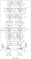
- FIG. 1 (a) and FIG. 1 (b) are a schematic diagram of a single-mode polarization multiplexing coherent receiver.
- a signal processing procedure of the single-mode polarization multiplexing coherent receiver includes the following steps.
- An optical signal is split into signals x1 and y 1 through processing by a polarization beam splitter #1 in a polarization beam splitter (Polarization beam splitter) 101.
- x1 is sent to a frequency mixer #1 in a frequency mixer (Hybrid) 102, and y1 is sent to a frequency mixer #2 in the frequency mixer 102.
- Hybrid frequency mixer
- Local oscillator light (for example, generated by a local laser (local laser) or a transmitter) is split into signals x2 and y2 through processing by a polarization beam splitter #2 in the polarization beam splitter 101.
- x2 is sent to the frequency mixer #1 in the frequency mixer 102
- y2 is sent to the frequency mixer #2 in the frequency mixer 102.
- an optical signal or the local oscillator light has two polarization modes: transverse electric (transverse electric, TE) and transverse magnetic (transverse magnetic, TM), which may also be referred to as a polarization state X and a polarization state Y, or may also be referred to as a polarization direction X and a polarization direction Y
- the polarization state X and the polarization state Y are orthogonal to each other.
- a light beam in a single polarization state (a polarization state Y) becomes a light beam in a polarization state X.
- X and Y herein are not an x-axis and a y-axis in a narrow sense, but are two orthogonal directions in a broad sense, for example, a horizontal +45° direction and a vertical -45° direction.
- the frequency mixer #1 and the frequency mixer #2 output four signals.
- the four signals are used as input of a photoelectric detector (Photodiode) 103, and are separately input to a photoelectric detector #1 to a photoelectric detector #4.
- the photoelectric detector is configured to convert strength of an optical signal into strength of an electrical signal.
- An output signal of the photoelectric detector #1 is a signal Ix
- an output signal of the photoelectric detector #2 is a signal Qx
- an output signal of the photoelectric detector #3 is a signal Iy
- an output signal of the photoelectric detector #4 is a signal Qy.
- Ix, Qx, Iy, and Qy are converted by an analog-to-digital converter #1 to an analog-to-digital converter #4 in an analog-to-digital converter (analog-to-digital converter, ADC) 104 respectively, and digital signals Ix, Qx, Iy, and Qy obtained through analog-to-digital conversion are output.
- Ix and Qx are combined by a combination module #1 in a combination module 105 to obtain a complex-number signal X.
- Iy and Qy are combined by a combination module #2 in the combination module 105 to obtain a complex-number signal Y.
- the combination module in this application may also be referred to as an adder.
- the complex-number signal X is input to an FFT module #1 in an FFT module 106, and is processed by the FFT module #1 to obtain a frequency-domain signal X that has undergone fast Fourier transform.
- the complex-number signal Y is input to an FFT module #2 in the FFT module 106, and is processed by the FFT module #2 to obtain a frequency-domain signal Y that has undergone fast Fourier transform.
- the frequency-domain signal X is input to a chromatic dispersion compensation module #1 in a chromatic dispersion compensation (Chromatic dispersion compensation, CDC) module 112, and chromatic dispersion compensation is performed in frequency domain to obtain a frequency-domain signal X that has undergone the frequency-domain dispersion compensation.
- the frequency-domain signal Y is input to a chromatic dispersion compensation module #2 in the chromatic dispersion compensation module 112, and chromatic dispersion compensation is performed in frequency domain to obtain a frequency-domain signal Y that has undergone the frequency-domain chromatic dispersion compensation.
- the frequency-domain signal X obtained through frequency-domain chromatic dispersion compensation is input to a clock recovery module #1 in a clock recovery module 107, and clock recovery is performed to obtain a frequency-domain signal X that has undergone the clock recovery.
- the frequency-domain signal Y obtained through frequency-domain chromatic dispersion compensation is input to a clock recovery module #2 in the clock recovery module 107, and clock recovery is performed to obtain a frequency-domain signal Y that has undergone the clock recovery.
- the frequency-domain signal X obtained through clock recovery is input to an IFFT module #1 in an IFFT module 113, and is processed by the IFFT module #1 to obtain a time-domain signal X that has undergone inverse fast Fourier transform.
- the frequency domain signal Y obtained through clock recovery is input to an IFFT module #2 in the IFFT module 113, and is processed by the IFFT module #2 to obtain a time-domain signal Y that has undergone inverse fast Fourier transform.
- Both the time-domain signal X and the time-domain signal Y are input to a polarization compensation module 108.
- the polarization compensation module includes 2 ⁇ 2 butterfly filters, and performs polarization demultiplexing and impairment equalization to obtain a time-domain signal X and a time-domain signal Y that have undergone polarization compensation.
- the polarization compensation module 108 further includes a coefficient update module 109.
- the coefficient update module 109 is configured to update a coefficient of a filter included in the polarization compensation module 108.
- the complex-number signal X obtained through polarization compensation is sequentially sent to a phase recovery module #1 in a phase recovery (phase recovery) module 110 and a decoding module #1 in a decoding (decoder) module 111 to obtain a bit signal.
- the complex-number signal Y obtained through polarization compensation is sequentially sent to a phase recovery module #2 in the phase recovery module 110 and a decoding module #2 in the decoding module 111 to obtain a bit signal.
- This embodiment of this application mainly relates to improvement of a processing procedure after the ADC. Therefore, for ease of description, the processing procedure after the ADC is collectively referred to as a receiver digital signal processing (Receiver Digital Signal Processing, Rx DSP) procedure, for example, an Rx DSP signal processing procedure included in a large dashed-line box in FIG. 1 (a) and FIG. 1 (b) .
- Rx DSP Receiveiver Digital Signal Processing
- a transmission mode that is, an HE 11 mode, for an optical signal in a single-mode optical fiber includes two sub-modes: HE x 11 and HE y 11 .
- the two sub-modes are independent of each other, and their polarization directions are orthogonal to each other.
- the two sub-modes present different forms in a transmission process: linear polarization, elliptical polarization, and circular polarization, but always remain orthogonal.
- X-polarization and Y-polarization in this application are two orthogonal polarization states in a multiplexing single-mode optical fiber.
- a multi-mode optical fiber can transmit signals in a plurality of modes.
- an LP pq mode is commonly used. Values of p and q represent different mode field characteristics of an LP mode.
- NTT processing and FFT processing in this application belong to transformation for implementing fast convolution.
- multiplication complexity of the complex number is quite high.
- NTT transformation is transformation that is defined in a finite field and whose core is K (K is an integer). Usually, K is 2. Therefore, a transformation matrix has no truncation error.
- K is an integer
- K is 2. Therefore, a transformation matrix has no truncation error.
- both multiplication and division of 2 can be implemented through shifting, so that multiplication can be avoided and power consumption can be reduced.
- the INTT processing is an inverse process of the NTT processing
- IFFT is an inverse process of the FFT processing. Details are not described in this application.
- a time-domain signal in the embodiments of this application is a signal that is input to an Rx DSP process through analog-to-digital conversion.
- a signal obtained by performing FFT processing on the time-domain signal is referred to as a frequency-domain signal, and a signal obtained through NTT processing is referred to as a transform-domain signal.
- a time-domain signal is obtained by performing IFFT processing on the frequency-domain signal, and a time-domain signal is obtained by performing INTT processing on the transform-domain signal.
- the time-domain signal in this application may be understood as a signal at a time granularity, and may change as time changes;
- the frequency-domain signal may be understood as a frequency-domain representation into which a time-domain signal is converted through transformation from time domain to frequency domain;
- the transform-domain signal may be understood as a transform-domain representation into which a time-domain signal is converted through transformation from time domain to transform domain.
- a time-domain signal is usually segmented, then a part is superposed at a beginning and an end, and then the signal is sent to an NTT/INTT transformation module.
- a segment of time-domain data includes 1024 points.
- a time-domain signal is first divided into 512 points, then 256 points are superposed at a beginning and an end, and then the 1024 points are sent to the NTT/INTT transformation module.
- 512, 256, and 1024 herein are merely examples.
- a specific superposition proportion and a specific quantity of points in a segment are not limited in this application.
- a quantity of points of data transformation is an array length during the data transformation. Generally, a larger quantity of points contributes to better transformation performance.
- Quadrature amplitude modulation is widely used in modern coherent communications.
- the quadrature amplitude modulation is a modulation scheme in which amplitude modulation is performed on two orthogonal carriers.
- the two carriers are usually sine waves with a phase difference of 90°, and therefore are referred to as orthogonal carriers.
- the real part of a complex-number signal is referred to as a codirectional component, and the imaginary part of the signal is referred to as a quadrature component.
- both a real part and an imaginary part of a complex-number signal are real numbers (for example, both a and b are real numbers). Therefore, in this application, the codirectional component is referred to as an in-phase real-number signal, and the quadrature component is referred to as a quadrature real-number signal.
- the embodiments of this application provide a signal processing method and apparatus, in which an electrical signal is processed without introducing the FFT module or the IFFT module, thereby improving performance of the polarization multiplexing coherent receiver in processing an electrical signal and reducing complexity.
- the signal processing method provided in the embodiments of this application may be used by a polarization multiplexing coherent receiver to process an electrical signal in a single-mode or multi-mode transmission scenario.
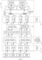
- FIG. 2 is a schematic diagram of an Rx DSP architecture according to an embodiment of this application.
- the Rx DSP architecture 200 includes: a first NTT module 211, a first chromatic dispersion compensation module 212, a clock recovery module 213, a first polarization compensation module 214, a first INTT module 215, a combination module 216, a phase recovery module 217, and a decoding module 218.
- the first NTT module includes an NTT module #1, an NTT module #2, an NTT module #3, and an NTT module #4.
- Signals I 1 x , Q 1 x , I 1 y , and Q 1 y are input to the NTT module #1, the NTT module #2, the NTT module #3, and the NTT module #4 respectively.
- the signals I 1 x , Q 1 x , I 1 y , and Q 1 y are real-number signals obtained through conversion by an ADC.
- the NTT module #1, the NTT module #2, the NTT module #3, and the NTT module #4 perform NTT processing on I 1 x , Q 1 x , I 1 y , and Q 1 y respectively, and output transform-domain first real-number signals Ix_1, Qx_1, Iy_1, and Qy_1 to the first chromatic dispersion compensation module 212.
- the first chromatic dispersion compensation module 212 includes a chromatic dispersion compensation module #1 and a chromatic dispersion compensation module #2.
- Ix_1 and Qx_1 are input to the chromatic dispersion compensation module #1, and chromatic dispersion compensation is performed to obtain transform-domain third real-number signals Ix_3 and Qx_3.
- Iy_1 and Qy_1 are input to the chromatic dispersion compensation module #2, and chromatic dispersion compensation is performed to obtain transform-domain third real-number signals Iy _3 and Qy_3.
- the clock recovery module 213 includes a clock recovery module #1 and a clock recovery module #2.
- Ix_3 and Qx_3 are input to the clock recovery module #1, and clock recovery is performed to obtain transform-domain second real-number signals Ix_2 and Qx_2.
- Iy_3 and Qy_3 are input to the clock recovery module #2, and clock recovery is performed to obtain transform-domain second real-number signals Iy_2 and Qy_2.
- the second real-number signals Ix_2, Qx_2, Iy_2, and Qy_2 are input to the first polarization compensation module 214, and polarization demultiplexing and impairment equalization are performed to obtain transform-domain sixth real-number signals Ix_5, Qx_5, Iy_5, and Qy_5.
- the first polarization compensation module 214 further includes a coefficient update module 2141.
- the coefficient update module 2141 is configured to update a coefficient of a filter included in the first polarization compensation module 214.
- the first INTT module 215 includes an INTT module #1, an INTT module #2, an INTT module #3, and an INTT module #4.
- Signals Ix_5, Qx_5, Iy_5, and Qy_5 are input to the INTT module #1, the INTT module #2, the INTT module #3, and the INTT module #4 respectively.
- the INTT module #1, the INTT module #2, the INTT module #3, and the INTT module #4 perform INTT processing on Ix_5, Qx_5, Iy_5, and Qy_5 respectively, and output time-domain seventh real-number signals Ix_6, Qx_6, Iy_6, and Qy_6 to the combination module 216.
- the combination module 216 includes a combination module #1 and a combination module #2.
- Ix_6 and Qx _6 are input to the combination module #1, and are combined to obtain a time-domain complex-number signal X.
- Iy_6 and Qy_6 are input to the combination module #2, and are combined to obtain a time-domain complex-number signal Y
- the phase recovery module 217 includes a phase recovery module #1 and a phase recovery module #2.
- the decoding module 111 includes a decoding module #1 and a decoding module #2.
- the time-domain complex-number signal X is sequentially input to the phase recovery module #1 and the decoding module #1 to obtain a recovered bit signal.
- the time-domain complex-number signal Y is sequentially input to the phase recovery module #2 and the decoding module #2 to obtain a recovered bit signal.
- the Rx DSP architecture 200 shown in FIG. 2 may be referred to as a full-transform-domain Rx DSP architecture.
- the full-transform-domain Rx DSP architecture not only performs chromatic dispersion compensation based on NTT/INTT, but also performs polarization compensation based on NTT/INTT, that is, performs chromatic dispersion compensation and polarization compensation in transform domain.
- polarization equalization impairment compensation is performed in transform domain, and multiplication is used to replace convolution, so that power consumption can be further reduced.
- a quantity (size) of transformation points can be increased, so that an impairment is effectively equalized and performance is improved.
- FIG. 3 is a schematic diagram of another Rx DSP architecture according to an embodiment of this application.
- the Rx DSP architecture 300 includes: a first NTT module 211, a first chromatic dispersion compensation module 212, a clock recovery module 213, a second polarization compensation module 310, a coefficient update module 311, a first INTT module 215, a combination module 216, a phase recovery module 320, and a decoding module 330.
- Modules before clock recovery in the architecture 300 are the same as those in the architecture 200. A difference lies in that a signal output by the clock recovery module 213 is first processed by the INTT module 215 and combined by the combination module 216, and then input to the second polarization compensation module 310. A process before the clock recovery is not described again.
- the first INTT module 215 includes an INTT module #1, an INTT module #2, an INTT module #3, and an INTT module #4.
- Second real-number signals Ix_2, Qx_2, Iy_2, and Qy_2 are input to the INTT module #1, the INTT module #2, the INTT module #3, and the INTT module #4 respectively.
- the INTT module #1, the INTT module #2, the INTT module #3, and the INTT module #4 perform INTT processing on Ix_2, Qx_2, Iy_2, and Qy_2 respectively, and output time-domain eighth real-number signals Ix_7, Qx_7, Iy_7, and Qy_7 to the combination module 216.
- the combination module 216 includes a combination module #1 and a combination module #2.
- Ix_7 and Qx _7 are input to the combination module #1, and are combined to obtain a time-domain complex-number signal X.
- Iy_7 and Qy_7 are input to the combination module #2, and are combined to obtain a time-domain complex-number signal Y.
- the time-domain complex-number signal X and the time-domain complex-number signal Y are input to the second polarization compensation module 310, and polarization demultiplexing and impairment equalization are performed to obtain a time-domain complex-number signal X and a time-domain complex-number signal Y that have undergone polarization compensation.
- the second polarization compensation module 310 further includes a coefficient update module 311.
- the coefficient update module 311 is configured to update a coefficient of a filter included in the second polarization compensation module 310.
- the phase recovery module 320 includes a phase recovery module #1 and a phase recovery module #2.
- the decoding module 111 includes a decoding module #1 and a decoding module #2.
- the time-domain complex-number signal X obtained through polarization compensation is sequentially input to the phase recovery module #1 and the decoding module #1 to obtain a recovered bit signal.
- the time-domain complex-number signal Y obtained through polarization compensation is sequentially input to the phase recovery module #2 and the decoding module #2 to obtain a recovered bit signal.
- the Rx DSP architecture 300 shown in FIG. 3 may be referred to as an Rx DSP architecture combining time domain and transform domain.
- chromatic dispersion compensation is performed based on NTT/INTT, and polarization compensation is still performed in time domain, that is, chromatic dispersion compensation is performed in transform domain but polarization compensation is performed in time domain.
- a chromatic dispersion compensation module with quite high power consumption implements compensation in transform domain, so that overall power consumption can be effectively reduced, and a polarization equalization module is left in time domain to perform compensation, so that a capability of the equalization module in resisting a loop delay is enhanced.
- FIG. 4 (a) is a schematic structural diagram of a chromatic dispersion compensation module 400.
- the chromatic dispersion compensation module 400 may be applied to the architecture shown in FIG. 1 (a) and FIG. 1 (b) .
- the chromatic dispersion compensation module includes an FFT module 402, an FFT module 404, a combination module 401, a combination module 403, and a multiplication module 405.
- Signals are transmitted in an optical fiber. Impact of chromatic dispersion of the optical fiber on the signals may be described as an impulse response.
- a finite impulse response finite impulse response (finite impulse response, FIR) is used for compensation.
- ⁇ 2 indicates a chromatic dispersion coefficient of an optical fiber
- z indicates a transmission distance of a signal in the optical fiber
- j indicates an imaginary number
- t indicates time. Because a signal in a polarization direction x and a signal in a polarization direction y undergo a same chromatic dispersion impairment, a same function h(t) is used during equalization.
- input of the chromatic dispersion compensation module is a frequency-domain complex-number signal X ( ⁇ ).
- I h (t) and Q h (t) are time-domain chromatic dispersion impulse responses
- I h (t) and Q h (t) are combined by the combination module 403 into a complex-number impulse response H(t)
- H(t) is input to the FFT module 404 to obtain a frequency-domain equalization function H( ⁇ )
- H( ⁇ ) and X( ⁇ ) are input to the multiplication module 405, and are multiplied to obtain output of the chromatic dispersion compensation module:
- X ⁇ ut( ⁇ ) H( ⁇ ).X( ⁇ ).
- FIG. 4 (b) is a schematic structural diagram of a chromatic dispersion compensation module 410 according to an embodiment of this application.
- the chromatic dispersion compensation module 410 may be applied to the RX DSP architectures 200 and 300.
- the chromatic dispersion compensation module includes an NTT module 411, an NTT module 412, an NTT module 419, an NTT module 420, a combination module 414, a combination module 418, a multiplication module 413, a multiplication module 415, a multiplication module 416, and a multiplication module 417.
- the NTT-based chromatic dispersion compensation module separately performs chromatic dispersion compensation on a signal in a polarization direction x and a signal in a polarization direction y.
- a chromatic dispersion compensation process (as shown in FIG. 4 (b) ) is described by using chromatic dispersion compensation in the polarization direction x as an example.
- I h (t) and Q h (t) are input to the NTT module 419 and the NTT module 420 respectively, and are transformed to obtain chromatic dispersion equalization functions I h (w) and Q h (w) in NTT transform domain.
- a codirectional signal Ix(t) and a quadrature signal Qx(t) in the polarization direction x are input to the NTT module 411 and the NTT module 412 respectively, and are transformed to obtain transform-domain signals I x (w) and Q x (w).
- a codirectional signal I y (t) and a quadrature signal Q y (t) in the polarization direction y are input to NTT modules, and are transformed to obtain transform-domain signals I y (w) and Q y (w) respectively.
- the equalization function H( ⁇ ) in Fourier transform domain in FIG. 4 (a) and the chromatic dispersion equalization functions I h (w) and Q h (w) in number theoretic transform domain in FIG. 4 (b) need to be calculated only once and stored in a memory, and may be repeatedly invoked for different input signals.
- NTT transformation and one FFT transformation are used as examples to explain a difference between the two types of transformations:
- a difference lies in a transformation core ⁇ e ⁇ j 2 ⁇ N of FFT.
- a transformation core ⁇ of NTT is a power of 2.
- ⁇ is 2 (or may be 2 or another value, which is not limited in this application).
- ⁇ 2 .
- Each element in a transformation matrix is still a power of 2, and multiplication by 2 or a power of 2 in a binary operation may be performed through bit shifting.
- FIG. 5 is a schematic diagram of still another Rx DSP architecture according to an embodiment of this application.
- the Rx DSP architecture 500 includes: a digital back propagation (digital back propagation, DBP) module 510, a first NTT module 211, a clock recovery module 213, a first polarization compensation module 214, a first INTT module 215, a combination module 216, a phase recovery module 217, and a decoding module 218.
- DBP digital back propagation
- An architecture after the first polarization compensation module 214 in the Rx DSP architecture 500 is the same as that in the Rx DSP architecture 200. A difference lies in that a signal undergoes DBP processing before polarization compensation. Because the DBP module 510 has a chromatic dispersion compensation function, a process after the DBP module may not require the chromatic dispersion compensation module 212.
- Signals I 1 x , Q 1 x , I 1 y , and Q 1 y are input to the DBP module 510, DBP processing is performed, and time-domain tenth real-number signals Ix_4, Qx_4, Iy_4, and Qy_4 are output to the first NTT module 211.
- the first NTT module 211 includes an NTT module #1, an NTT module #2, an NTT module #3, and an NTT module #4.
- Ix_4, Qx_4, Iy_4, and Qy_4 are input to the NTT module #1, the NTT module #2, the NTT module #3, and the NTT module #4 respectively.
- the NTT module #1, the NTT module #2, the NTT module #3, and the NTT module #4 perform NTT processing on Ix_4, Qx_4, Iy_4, and Qy_4 respectively, and output transform-domain first real-number signals Ix_1, Qx_1, Iy_1, and Qy_1 to the clock recovery module 213.
- the clock recovery module 213 includes a clock recovery module #1 and a clock recovery module #2.
- Ix_1 and Qx_1 are input to the clock recovery module #1, and clock recovery is performed to obtain transform-domain second real-number signals Ix_2 and Qx_2.
- Iy_1 and Qy_1 are input to the clock recovery module #2, and clock recovery is performed to obtain transform-domain second real-number signals Iy_2 and Qy_2.
- the Rx DSP architecture 500 shown in FIG. 5 may be referred to as a full-transform-domain Rx DSP architecture in which DBP is added.
- a difference from the full-transform-domain Rx DSP architecture shown in FIG. 2 lies in that the DBP module is added.
- the DBP module is added in the full-transform-domain Rx DSP architecture shown in FIG. 2 .
- the DBP module is used to implement nonlinear-effect compensation on a basis of a linear impairment, to increase a signal transmission distance.
- FIG. 6 is a schematic diagram of still another Rx DSP architecture according to an embodiment of this application.
- the Rx DSP architecture 600 includes: a DBP module 510, a first NTT module 211, a clock recovery module 213, a second polarization compensation module 310, a coefficient update module 311, a first INTT module 215, a combination module 216, a phase recovery module 320, and a decoding module 330.
- An architecture after the second polarization compensation module 310 in the Rx DSP architecture 600 is the same as that in the Rx DSP architecture 300.
- An architecture before the second polarization compensation module 310 is the same as that in the Rx DSP architecture 500.
- a received signal obtained through conversion by an ADC first undergoes DBP processing.
- DBP processing and clock recovery refer to the embodiment shown in FIG. 5 .
- clock recovery module 213 refer to the embodiment shown in FIG. 3 .
- the Rx DSP architecture 600 shown in FIG. 6 may be referred to as an Rx DSP architecture combining time domain and transform domain in which DBP is added.
- a difference from the Rx DSP architecture combining time domain and transform domain shown in FIG. 3 lies in that the DBP module is added.
- the DBP module is added in the Rx DSP architecture combining time domain and transform domain shown in FIG. 3 .
- only a linear impairment of an optical fiber is compensated for, for example, chromatic dispersion compensation.
- the DBP module is used to implement nonlinear-effect compensation on a basis of a linear impairment, to increase a signal transmission distance.
- FIG. 7 is a schematic structural diagram of a DBP module according to an embodiment of this application.
- the DBP module 700 includes: a second NTT module 711, a second chromatic dispersion compensation module 712, a second INTT module 713, and a nonlinear compensation module 714, where a structure of the second chromatic dispersion compensation module 712 is shown in FIG. 4 (b) , and is not described in detail herein.
- the second NTT module 711 includes an NTT module #1, an NTT module #2, an NTT module #3, and an NTT module #4.
- I 1 x , Q 1 x , I 1 y , and Q 1 y are input to the NTT module #1, the NTT module #2, the NTT module #3, and the NTT module #4 respectively.
- the NTT module #1, the NTT module #2, the NTT module #3, and the NTT module #4 perform NTT processing on I 1 x , Q 1 x , I 1 y , and Q 1 y respectively, and output fourth real-number signals Ix_4', Qx_4', Iy_4', and Qy_4' to the second chromatic dispersion compensation module 712.
- the second chromatic dispersion compensation module 712 includes a chromatic dispersion compensation module #1 and a chromatic dispersion compensation module #2.
- Ix_4' and Qx_4' are input to the chromatic dispersion compensation module #1, and chromatic dispersion compensation is performed in transform domain to obtain transform-domain fifth real-number signals Ix_4" and Qx_4".
- Iy_4' and Qy_4' are input to the chromatic dispersion compensation module #2, and chromatic dispersion compensation is performed in transform domain to obtain transform-domain fifth real-number signals Iy_4" and Qy_4".
- the second INTT module 713 includes an INTT module #1, an INTT module #2, an INTT module #3, and an INTT module #4.
- Ix_4", Qx_4", Iy_4", and Qy_4" are input to the INTT module #1, the INTT module #2, the INTT module #3, and the INTT module #4 respectively.
- the INTT module #1, the INTT module #2, the INTT module #3, and the INTT module #4 perform INTT processing on Ix_4", Qx_4", Iy_4", and Qy_4" respectively, and output time-domain ninth real-number signals Ix_4′′′, Qx_4′′′, Iy_4′′′, and Qy_4′′′ to the nonlinear compensation module 714.
- the nonlinear compensation module 714 includes a nonlinear compensation module #1 and a nonlinear compensation module #2.
- Ix_4' and Qx_4' are input to the nonlinear compensation module #1, and nonlinear compensation is performed to obtain Ix_4 and Qx_4.
- Iy_4' and Qy_4' are input to the nonlinear compensation module #2, and nonlinear compensation is performed to obtain Iy_4 and Qy_4.
- Ns may be set to be equal to a total span of a link, or single-step DBP may be set.
- no FFT module or IFFT module is used; instead, the NTT module and the INTT module are used. In this way, during a signal processing procedure of the DBP module, repeated Ns transformations do not cause error accumulation.
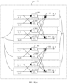
- FIG. 8 (a) is a schematic structural diagram of a first polarization compensation module 214 according to an embodiment of this application.
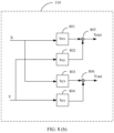
- FIG. 8 (b) is a schematic structural diagram of a second polarization compensation module 310 according to an embodiment of this application.
- the first polarization compensation module 214 in this embodiment of this application includes a butterfly filter 810 and a butterfly filter 820.
- the butterfly filter 810 includes a filter 801, a filter 802, a filter 803, a filter 804, an adder 805, and an adder 806.
- the butterfly filter 820 includes a filter 807, a filter 808, a filter 809, a filter 8010, an adder 8011, and an adder 8012.
- Output of the filter 801, output of the filter 807, output of the filter 803, and output of the filter 809 are negative.
- the foregoing four signals are input to the adder 805 to obtain a signal Ix_5 that has undergone chromatic dispersion compensation.
- the output of the filter 801, the output of the filter 807, the output of the filter 803, and the output of the filter 809 are input to the adder 805 to obtain a signal Qx_5 that has undergone chromatic dispersion compensation.
- Output of the filter 802, output of the filter 808, output of the filter 804, and output of the filter 8010 are negative.
- the foregoing four signals are input to the adder 806 to obtain a signal Iy_5 that has undergone chromatic dispersion compensation.
- the output of the filter 802, the output of the filter 808, the output of the filter 804, and the output of the filter 8010 are output to the adder 805 to obtain a signal Qy_5 that has undergone chromatic dispersion
- a clock recovery module outputs four signals.
- the four signals Ix_2, Qx_2, Iy_2, and Qy_2 are input to a polarization compensation module.
- the polarization compensation module includes two butterfly filters.
- One butterfly filter represents a 2 ⁇ 2 two-input, two-output system.
- Two complex-number signals are input, and two complex-number signals are output. Because real-number signals are processed in NTT transformation, a polarization equalization part is a 4 ⁇ 4 four-input, four-output system.
- the first butterfly filter 810 is for equalization and depolarization of I-path signals (including an x-polarization I-path signal Ix_2 and a y-polarization I-path signal Iy_2), and a transformation matrix is I hxx I hxy I hyx I hyy .
- the second butterfly filter 820 is for Q-path signals (including an x-polarization Q-path signal Qx_2 and a y-polarization Q-path signal Qy_2), and a transformation matrix is Q hxx Q hxy Q hyx Q hyyy .
- the polarization compensation module outputs four real-number signals: Ix_5, Qx_5, Iy_5, and Qy_5.
- a process of performing polarization compensation by the first polarization compensation module 214 is described with reference to FIG. 8 (a) .
- Input signals of the first polarization compensation module 214 are four real-number signals: Ix_2, Qx_2, Iy_2, and Qy_2, which are a codirectional signal Ix_2 in a polarization direction x, a quadrature signal Qx_2 in the polarization direction x, a codirectional signal Iy_2 in a polarization direction y, and a quadrature signal Qy_2 in the polarization direction y, respectively.
- a multiplication result of Ix_2 and I hxx is input to the adder 805, a negative value of a multiplication result of Qx_2 and Q hxx is input to the adder 805, a multiplication result of Iy_2 and I hxy is input to the adder 805, a negative value of a multiplication result of Qy_2 and Q hxy is input to the adder 805, and the adder 805 outputs a codirectional signal Ix_5 that is in the polarization direction x and that is obtained through polarization compensation.
- a multiplication result of Ix_2 and Q hxx is input to the adder 8011, a negative value of a multiplication result of Qx_2 and I hxx is input to the adder 8011, a multiplication result of Iy_2 and Q hxy is input to the adder 8011, a multiplication result of Qy_2 and I hxy is input to the adder 8011, and the adder 8011 outputs a quadrature signal Qx_5 that is in the polarization direction x and that is obtained through polarization compensation.
- a multiplication result of Ix_2 and I hyx is input to the adder 806, a negative value of a multiplication result of Qx_2 and Q hyx is input to the adder 806, a multiplication result of Iy_2 and I hyy is input to the adder 806, a negative value of a multiplication result of Qy_2 and Q hyy is input to the adder 806, and the adder 806 outputs a codirectional signal Iy_5 that is in the polarization direction y and that is obtained through polarization compensation.
- a multiplication result of Ix_2 and Q hyx is input to the adder 8012, a multiplication result of Qx_2 and I hyx is input to the adder 8012, a multiplication result of Iy_2 and Q hyy is input to the adder 8012, a multiplication result of Qy_2 and I hyy is input to the adder 8012, and the adder 8012 outputs a quadrature signal Qy_5 that is in the polarization direction y and that is obtained through polarization compensation.
- the first polarization compensation module 214 further includes a coefficient update module 2141 (not shown in the figure).
- the coefficient update module 2141 is configured to update a coefficient of a filter included in the first polarization compensation module 214.
- manners of updating equalization coefficient matrices I hxx I hxy I hyx I hyy and Q hxx Q hxy Q hyx Q hyy of a polarization compensation module include a blind update, an update with training, an update without decision feedback, an update with decision feedback, and the like.
- a manner of updating a coefficient of the polarization compensation module is not limited in this embodiment of this application. Details are not described herein.
- the second polarization compensation module 310 in this embodiment of this application includes 2 ⁇ 2 butterfly filters, and the butterfly filters include a filter 801, a filter 802, a filter 803, a fourth filter 804, an adder 805, and an adder 806.
- Functions of the second polarization compensation module 310 include channel optical fiber effects such as equalization compensation (equalization compensation), a differential group delay (differential group delay, DGD), and residual chromatic dispersion.
- An optical fiber effect may be described by using a 2 ⁇ 2 impairment matrix.
- An inverse matrix of the impairment matrix may be obtained by using different algorithms.
- Tap coefficients of a time-domain butterfly filter 108 are hxx, hxy, hyx, and hyy.
- X and Y signals are convolved with the tap coefficient matrices hxx, hxy, hyx, and hyy to obtain signals Xout and Yout that have undergone polarization impairment compensation.
- Common algorithms for calculating a tap coefficient matrix include a constant modulus algorithm (constant modulus algorithm, CMA), a least mean square (Least Mean Square, LMS), and various modified versions of the LMS or other forms such as a data-aided LMS.
- the combination module 216 outputs a complex-number signal X in a polarization direction X, and the complex-number signal X is input to the filter 801 and the filter 803.
- the combination module 216 outputs a complex-number signal Y in a polarization direction Y, and the complex-number signal Y is input to the filter 802 and the filter 804.
- the filter 801 and the filter 803 provide output to the adder 805.
- the filter 802 and the filter 804 provide output to the adder 806.
- hxx, hxy, hyx, and hyy in FIG. 8 (b) represent coefficients of the filter 801, the filter 802, the filter 803, and the filter 804 respectively.
- FIG. 8 (a) and FIG. 8 (b) are used as examples to describe the butterfly filters in this application, the butterfly filters shown in FIG. 8 (a) and FIG. 8 (b) are merely examples, and do not constitute any limitation on the protection scope of this application.
- the butterfly filters in the embodiments of this application should be understood in a broad sense, and a filter or a filter combination that can implement a deconvolution function may be referred to as a butterfly filter.
- the Rx DSP provided in this embodiment of this application may be further applied to a multi-mode transmission scenario.
- the Rx DSP is applied to m transmission modes.
- the Rx DSP receives P real-number signals.
- FIG. 9 (a) is a schematic diagram of an Rx DSP architecture in a multi-mode transmission scenario according to an embodiment of this application.
- the Rx DSP architecture 900 includes: a first NTT module 211, a first chromatic dispersion compensation module 212, a clock recovery module 213, a first polarization compensation module 214, a first INTT module 215, a combination module 216, a phase recovery module 217, and a decoding module 218.
- P real-number signals are input to the first NTT module 211.
- the first NTT module separately performs NTT processing on the P real-number signals, and outputs P transform-domain first real-number signals to the first chromatic dispersion compensation module 212.
- the P real-number signals are real-number signals obtained through conversion by an ADC.
- the P real-number signals include 4 ⁇ m real-number signals in m transmission modes.
- the first chromatic dispersion compensation module 212 separately performs chromatic dispersion compensation on the P transform-domain first real-number signals, and outputs P transform-domain third real-number signals to the clock recovery module 213.
- the clock recovery module 213 separately performs clock recovery on the P transform-domain third real-number signals, and outputs P transform-domain second real-number signals to the first polarization compensation module 214.
- the first polarization compensation module 214 performs polarization compensation processing on the P transform-domain second real-number signals, and outputs P transform-domain sixth real-number signals to the first INTT module 215.
- the first INTT module 215 separately performs INTT processing on the P transform-domain sixth real-number signals, and outputs P time-domain seventh real-number signals to the combination module 216.
- the combination module 216 combines the P time-domain seventh real-number signals, and outputs m complex-number signals X and m complex-number signals Y to the phase recovery module 217 and the decoding module 218.
- the phase recovery module 217 and the decoding module 218 perform phase recovery and decoding processing on the m complex-number signals X and the m complex-number signals Y to obtain recovered bit signals.
- FIG. 9 (b) is a schematic diagram of an Rx DSP architecture in another multi-mode transmission scenario according to an embodiment of this application.
- the Rx DSP architecture 910 includes: a first NTT module 211, a first chromatic dispersion compensation module 212, a clock recovery module 213, a second polarization compensation module 108, a first INTT module 215, a combination module 216, a phase recovery module 320, and a decoding module 330.
- Modules before clock recovery in the architecture 910 are the same as those in the architecture 900. A difference lies in that a signal output by the clock recovery module is first processed by the INTT module and combined by the combination module, and then input to the second polarization compensation module 108. A process before the clock recovery is not described again.
- the first INTT module 215 separately performs INTT processing on the P transform-domain second real-number signals, and outputs P time-domain eighth real-number signals to the combination module 216.
- the combination module 216 combines the P time-domain eighth real-number signals, and outputs m complex-number signals X and m complex-number signals Y to the second polarization compensation module 310.
- the second polarization compensation module 310 performs polarization compensation processing on the m complex-number signals X and the m complex-number signals Y, and outputs m time-domain complex-number signals X and m time-domain complex-number signals Y obtained through polarization compensation to the phase recovery module 320 and the decoding module 330.
- the second polarization compensation module 310 further includes a coefficient update module 311 (not shown in the figure).
- the coefficient update module 311 is configured to update a coefficient of a filter included in the second polarization compensation module 310.
- the phase recovery module 320 and the decoding module 330 perform phase recovery and decoding processing on the m complex-number signals X and the m complex-number signals Y to obtain recovered bit signals.
- FIG. 9 (c) is a schematic diagram of an Rx DSP architecture in still another multi-mode transmission scenario according to an embodiment of this application.
- the Rx DSP architecture 920 includes: a DBP module 510, a first NTT module 211, a clock recovery module 213, a first polarization compensation module 214, a first INTT module 215, a combination module 216, a phase recovery module 217, and a decoding module 218.
- An architecture after the first polarization compensation module 214 in the Rx DSP architecture 920 is the same as that in the Rx DSP architecture 900. A difference lies in that a signal undergoes DBP processing before polarization compensation. Because the DBP module 510 has a chromatic dispersion compensation function, a process after the DBP module may not require the chromatic dispersion compensation module 212.
- P real-number signals are input to the DBP module 510, DBP processing is performed, and P time-domain tenth real-number signals are output to the first NTT module 211.
- the first NTT module 211 separately performs NTT processing on the P time-domain tenth real-number signals, and outputs P transform-domain first real-number signals to the clock recovery module 213.
- the clock recovery module 213 separately performs clock recovery processing on the P transform-domain first real-number signals, and outputs P transform-domain second real-number signals to the first polarization compensation module 214.
- FIG. 9 (d) is a schematic diagram of an Rx DSP architecture in still another multi-mode transmission scenario according to an embodiment of this application.
- the Rx DSP architecture 930 includes: a DBP module 510, a first NTT module 211, a clock recovery module 213, a second polarization compensation module 310, a first INTT module 215, a combination module 216, a phase recovery module 320, and a decoding module 330.
- An architecture after the second polarization compensation module 310 in the Rx DSP architecture 930 is the same as that in the Rx DSP architecture 910.
- An architecture before the second polarization compensation module 310 is the same as that in the Rx DSP architecture 920.
- a received signal obtained through conversion by an ADC first undergoes DBP processing.
- a process before the DBP processing and clock recovery refer to the embodiment shown in FIG. 9 (c) .
- FIG. 9 (e) is a schematic structural diagram of another DBP module according to an embodiment of this application.
- the DBP module 940 includes: a second NTT module 711, a second chromatic dispersion compensation module 712, a second INTT module 713, and a nonlinear compensation module 714.
- That P real-number signals are input to the DBP module 510, and DBP processing is performed to obtain P time-domain tenth real-number signals specifically includes the following steps.
- the P real-number signals are respectively input to P second NTT modules 711, NTT processing is performed, and P transform-domain fourth real-number signals are output to the second chromatic dispersion compensation module 712.
- the second chromatic dispersion compensation module 712 performs chromatic dispersion compensation processing on the P transform-domain fourth real-number signals, and outputs P transform-domain fifth real-number signals to the second INTT module 713.
- the second INTT module 713 performs INTT processing on the P transform-domain fifth real-number signals, and outputs P time-domain ninth real-number signals to the nonlinear compensation module 714.
- the nonlinear compensation module 714 performs nonlinear compensation on the P time-domain ninth real-number signals to obtain the P time-domain tenth real-number signals.
- performing signal processing by using the NTT module and the INTT module has the following advantages.
- complexity of signal processing performed based on the NTT module and the INTT module is proportional to 2Nlog2N additions.
- complexity of signal processing performed based on the NTT module and the INTT module is reduced to different degrees. For example, if a quantity of transformation points is 256, power consumption of NTT is reduced to approximately 1/4 of that of FFT.
- a transformation core of NTT is an integer and the transformation core is usually 2 or a power of 2
- the transformation core can be accurately expressed in a memory.
- a bit width of a transformation matrix is fixed, without a fixed-point penalty.
- a truncation error and a fixed-point penalty in a single FFT or IFFT transformation repeatedly accumulate during DBP propagation. As a result, a final result error is larger.
- a transformation core of NTT is 2, and a transformation matrix includes 2 or a power of 2.
- a number is multiplied by a power of 2 only through shifting. Therefore, no huge transformation matrix needs to be stored in a DSP process, and only the transformation core needs to be stored.
- FIG. 10 (a) is a schematic flowchart of a signal processing method according to an embodiment of this application. The following steps S1010 to S1050 are included.
- the P real-number signals include real-number signals that are in two polarization directions and that correspond to each of m modes. When m is equal to 1, it indicates single-mode transmission; or when m is greater than 1, it indicates multi-mode transmission. m and P are positive integers.
- At least NTT processing is performed on the P real-number signals to obtain the P transform-domain first real-number signals.
- the following two possible implementations are included.
- Implementation 1.1 Perform NTT processing on the P real-number signals to obtain the P transform-domain first real-number signals.
- Implementation 1.2 Sequentially perform DBP processing and NTT processing on the P real-number signals to obtain the P transform-domain first real-number signals.
- DBP processing is first performed on the P real-number signals to obtain P time-domain tenth real-number signals, and then NTT processing is performed on the P time-domain tenth real-number signals to obtain the P transform-domain first real-number signals.
- the performing NTT processing on the P real-number signals in the implementation 1.1, and the performing NTT processing on the P time-domain tenth real-number signals that are obtained by performing DBP processing on the P real-number signals in the implementation 1.2 may be collectively referred to as performing NTT processing on P input signals.
- the P input signals include the P real-number signals, or the P time-domain tenth real-number signals that are obtained by performing DBP processing on the P real-number signals.
- FIG. 10 (b) is a schematic flowchart of DBP processing according to an embodiment of this application. The following steps S1021 to S1024 are included.
- NTT processing is performed on P real-number signals to obtain the P transform-domain fourth real-number signals.
- Chromatic dispersion compensation is performed on the P transform-domain fourth real-number signals in transform domain to obtain the P transform-domain fifth real-number signals.
- INTT processing is performed on the P transform-domain fifth real-number signals to obtain the P time-domain ninth real-number signals.
- Nonlinear compensation is performed on the P time-domain ninth real-number signals to obtain the P time-domain tenth real-number signals.
- At least clock recovery processing is performed on the P transform-domain first real-number signals to obtain the P transform-domain second real-number signals.
- step S1020 the following two possible implementations are included.
- Implementation 2.1 This corresponds to the implementation 1.1 in step S1020.
- a processing procedure includes the following steps.
- the performing chromatic dispersion compensation on the P transform-domain first real-number signals to obtain P transform-domain third real-number signals specifically includes the following steps:
- a processing procedure includes the following step: Separately perform clock recovery on the P transform-domain first real-number signals to obtain the P transform-domain second real-number signals.
- At least polarization compensation processing and INTT processing are performed on the P transform-domain second real-number signals to obtain m time-domain complex-number signals X and m time-domain complex-number signals Y.
- m time-domain complex-number signals X and m time-domain complex-number signals Y are included.
- FIG. 10 (c) is a schematic flowchart of obtaining a time-domain complex-number signal according to an embodiment of this application. The following steps S1041 to S1043 are included.
- Polarization compensation is performed on P transform-domain second real-number signals to obtain the P transform-domain sixth real-number signals.
- INTT processing is separately performed on the P transform-domain sixth real-number signals to obtain the P time-domain seventh real-number signals.
- Every two of 2 ⁇ m time-domain seventh real-number signals that are in the P time-domain seventh real-number signals and that are in a first polarization direction are combined to obtain the m time-domain complex-number signals X in the first polarization direction.
- Every two of 2 ⁇ m time-domain seventh real-number signals that are in the P time-domain seventh real-number signals and that are in a second polarization direction are combined to obtain the m time-domain complex-number signals Y in the second polarization direction.
- FIG. 10 (d) is another schematic flowchart of obtaining a time-domain complex-number signal according to an embodiment of this application. The following steps S1044 to S1046 are included.
- INTT processing is performed on P transform-domain second real-number signals to obtain the P time-domain eighth real-number signals.
- Every two of 2 ⁇ m time-domain eighth real-number signals that are in the P time-domain eighth real-number signals and that are in a first polarization direction are combined to obtain the m time-domain complex-number signals X in the first polarization direction.
- Every two of 2 ⁇ m time-domain eighth real-number signals that are in the P time-domain eighth real-number signals and that are in a second polarization direction are combined to obtain the m time-domain complex-number signals Y in the second polarization direction.
- Polarization compensation is performed on the m time-domain complex-number signals X in the first polarization direction and the m time-domain complex-number signals Y in the second polarization direction to obtain the m time-domain complex-number signals X and the m time-domain complex-number signals Y that have undergone the polarization compensation.
- phase recovery and decoding need to be performed on the time-domain complex-number signals obtained in S1040.
- phase recovery is performed on the m time-domain complex-number signals X and the m time-domain complex-number signals Y to obtain m time-domain complex-number signals X and m time-domain complex-number signals Y that have undergone the phase recovery.
- the m time-domain complex-number signals X and the m time-domain complex-number signals Y that are obtained through phase recovery are decoded to obtain m time-domain complex-number signals X and m time-domain complex-number signals Y that have been decoded.
- phase recovery and decoding on the time-domain complex-number signals is not limited in this embodiment of this application.
- An embodiment of this application further provides a coherent receiver, including a polarization beam splitter, a frequency mixer, a photoelectric detector, an analog-to-digital converter, and the Rx DSP shown in FIG. 9 (a) , FIG. 9 (b) , FIG. 9 (c) , or FIG. 9 (d) .
- the polarization beam splitter, the frequency mixer, the photoelectric detector, and the analog-to-digital converter are similar to those shown in FIG. 1 (a) and FIG. 1 (b) . Details are not described herein again.
- FIG. 11 is a schematic diagram of a chip 1100 according to this application.
- the chip 1100 includes a processor 1110, a memory 1120, and a communications interface 1130.
- the processor 1110 is coupled to the memory 1120.
- the memory 1120 is configured to store a computer program or an instruction and/or data.
- the processor 1110 is configured to execute the computer program or the instruction and/or the data stored in the memory 1120, so that the method in the foregoing method embodiment is performed.
- the chip shown in FIG. 11 may be a signal processing apparatus including a processor 1110 and a communications interface 1130.
- the processor 1110 is coupled to a memory by using the communications interface 1130, and the processor 1110 is configured to perform the method in the foregoing method embodiment.
- the functions When the functions are implemented in the form of a software functional unit and sold or used as an independent product, the functions may be stored in a computer-readable storage medium. Based on such an understanding, the technical solutions of this application essentially, or the part contributing to the prior art, or some of the technical solutions may be implemented in a form of a software product.
- the software product is stored in a storage medium, and includes several instructions for instructing a computer device (which may be a personal computer, a server, or a network device) to perform all or some of the steps of the methods described in the embodiments of this application.
- the foregoing storage medium includes: any medium that can store program code, such as a USB flash drive, a removable hard disk, a read-only memory (read-only memory, ROM), a random access memory (random access memory, RAM), a magnetic disk, or an optical disc.
- program code such as a USB flash drive, a removable hard disk, a read-only memory (read-only memory, ROM), a random access memory (random access memory, RAM), a magnetic disk, or an optical disc.
Landscapes
- Physics & Mathematics (AREA)
- Electromagnetism (AREA)
- Engineering & Computer Science (AREA)
- Computer Networks & Wireless Communication (AREA)
- Signal Processing (AREA)
- Optical Communication System (AREA)
Description
- This application claims priority to Russian Patent Application No.
RU2020117812, filed on May 29, 2020 - This application relates to the optical communications field, and in particular, to a signal processing method and apparatus, and a coherent receiver.
- Performance of a high-capacity optical communications system may deteriorate due to optical fiber attenuation, optical fiber chromatic dispersion, polarization mode chromatic dispersion, laser phase noise, optical fiber nonlinearity, or the like. A currently provided polarization multiplexing coherent receiver can effectively compensate for the foregoing deterioration factors in electrical domain during an electrical signal processing procedure.
- During the electrical signal processing procedure of the existing polarization multiplexing coherent receiver, to implement the foregoing effective compensation in electrical domain, convolution of a time-domain signal and an inverse function of a channel response is implemented based on Fourier transform. Therefore, a fast Fourier transform (fast Fourier transform, FFT) module and an inverse fast Fourier transform (inverse fast Fourier transform, IFFT) module need to be introduced into a structure of the polarization multiplexing coherent receiver. However, the Fourier transform has high complexity and low precision. As a result, the electrical signal processing procedure is highly complex, and accuracy of a recovered signal is low. Therefore, how to improve performance of a polarization multiplexing coherent receiver in processing an electrical signal becomes an urgent problem to be resolved.
- An optical signal processing method according to the state of the art is known from
US-A-9225431 - This application provides a signal processing method and apparatus, and a coherent receiver, to improve signal processing performance.
- According to a first aspect, a signal processing method is provided. The signal processing method may be performed by a coherent receiver, or may be performed by a chip or a circuit disposed in a coherent receiver. This is not limited in this application.
- The signal processing method includes:
- first, obtaining P real-number signals, where the P real-number signals include P real-number signals obtained through analog-to-digital conversion or other P real-number signals that require digital signal processing, and this is not limited in this application;
- then, performing at least number theoretic transform (number theoretic transform, NTT) processing on the P real-number signals to obtain P transform-domain first real-number signals;
- then, performing at least clock recovery on the P transform-domain first real-number signals to obtain P transform-domain second real-number signals; and
- then, performing at least polarization compensation and inverse number theoretic transform (inverse number theoretic transform, INTT) processing on the P transform-domain second real-number signals to obtain m time-domain complex-number signals X and m time-domain complex-number signals Y, where m and P are positive integers.
- Further, if INTT and combination processing is first performed and then polarization compensation processing is performed, in the signal processing method provided in this application, phase recovery and decoding may be performed on m time-domain complex-number signals X and m time-domain complex-number signals Y that are obtained through polarization compensation, to obtain bit signals.
- It should be understood that if the INTT and combination processing is first performed and then the polarization compensation processing is performed, the polarization compensation processing is performed based on a time-domain signal obtained through INTT processing. Specifically, a capability of resisting a loop delay can be enhanced by performing polarization compensation processing in time domain.
- Alternatively, if polarization compensation processing is first performed and then INTT and combination processing is performed, in the signal processing method provided in this application, phase recovery and decoding may be performed on m time-domain complex-number signals X in a first polarization direction and m time-domain complex-number signals Y in a second polarization direction that are obtained through combination, to obtain bit signals, so as to implement signal recovery.
- It should be understood that if the polarization compensation processing is first performed and then the INTT and combination processing is performed, the polarization compensation processing is performed based on a transform-domain signal. Specifically, polarization equalization impairment compensation is performed in transform domain, and multiplication is used to replace convolution, so that power consumption can be reduced.
- In the signal processing method provided in this application, signals in two polarization directions are obtained through analog-to-digital conversion, and the signals in the two polarization directions are input to a receiver digital signal processing Rx DSP apparatus. During a processing procedure of the Rx DSP, number theoretic transform NTT and inverse number theoretic transform INTT processing is used to replace fast Fourier transform FFT and inverse fast Fourier transform IFFT processing, to avoid high complexity and low accuracy caused by the FFT and IFFT processing, thereby improving signal processing performance.
- With reference to the first aspect, in some implementations of the first aspect, the performing at least number theoretic transform NTT processing on the P real-number signals to obtain P transform-domain first real-number signals includes: performing NTT processing on the P real-number signals to obtain the P transform-domain first real-number signals; or
performing digital back propagation DBP processing on the P real-number signals to obtain P time-domain tenth real-number signals, and separately performing NTT processing on the P time-domain tenth real-number signals to obtain the P transform-domain first real-number signals. - If the P real-number signals undergo DBP processing, a DBP module is used to implement nonlinear-effect compensation, to increase a signal transmission distance.
- In the signal processing method provided in this application, the P transform-domain first real-number signals may be obtained by inputting the P real-number signals to an NTT module and performing NTT processing; or the P transform-domain first real-number signals may be obtained by first inputting the P real-number signals to the DBP module and performing DBP processing, and then performing NTT processing. Different manners of obtaining the P transform-domain first real-number signals are provided, so that a structural design of the Rx DSP apparatus is more flexible.
- With reference to the first aspect, in some implementations of the first aspect, when the P real-number signals do not undergo DBP processing, chromatic dispersion compensation needs to be performed when the P transform-domain second real-number signals are obtained based on the P transform-domain first real-number signals. To be specific, the performing at least clock recovery on the P transform-domain first real-number signals to obtain P transform-domain second real-number signals includes: performing chromatic dispersion compensation on the P transform-domain first real-number signals to obtain P transform-domain third real-number signals; and performing clock recovery on the P transform-domain third real-number signals to obtain the P transform-domain second real-number signals.
- Alternatively, when the P real-number signals undergo DBP processing, because the DBP module has a chromatic dispersion compensation function, no additional chromatic dispersion compensation needs to be performed when the P transform-domain second real-number signals are obtained based on the P transform-domain first real-number signals. To be specific, the performing at least clock recovery on the P transform-domain first real-number signals to obtain P transform-domain second real-number signals includes: performing chromatic dispersion compensation on the P transform-domain first real-number signals to obtain the P transform-domain second real-number signals.
- With reference to the first aspect, in some implementations of the first aspect, the P real-number signals include an in-phase real-number signal Im x and a quadrature real-number signal Qm x in the first polarization direction, and an in-phase real-number signal Im y and a quadrature real-number signal Qm y in the second polarization direction. In the foregoing case in which additional chromatic dispersion compensation is required, a chromatic dispersion compensation process includes: performing NTT processing on a chromatic dispersion impulse response Ih(t) corresponding to an in-phase real-number signal and a chromatic dispersion impulse response Qh(t) corresponding to a quadrature real-number signal, to obtain a transform-domain chromatic dispersion equalization function Ih(w) corresponding to the in-phase real-number signal and a transform-domain chromatic dispersion equalization function Qh(w) corresponding to the quadrature real-number signal.
- After Ih(w) and Qh(w) are obtained, 2×m transform-domain third real-number signals that are in the P transform-domain third real-number signals and that are in the first polarization direction can be determined based on Ih(w), Qh(w), and an in-phase real-number signal and a quadrature real-number signal that are in the P transform-domain first real-number signals and that are in the first polarization direction, and 2×m transform-domain third real-number signals that are in the P transform-domain third real-number signals and that are in the second polarization direction can be determined based on Ih(w), Qh(w), and an in-phase real-number signal and a quadrature real-number signal that are in the P transform-domain first real-number signals and that are in the second polarization direction, so as to complete chromatic dispersion compensation.
- With reference to the first aspect, in some implementations of the first aspect, the transform-domain third real-number signals obtained through chromatic dispersion compensation and the transform-domain first real-number signals meet the following requirements:


Ix(w) represents an in-phase real-number signal that is in the transform-domain first real-number signals and that is in the first polarization direction, Qx(w) represents a quadrature real-number signal that is in the transform-domain first real-number signals and that is in the first polarization direction, Iy(w) represents an in-phase real-number signal that is in the transform-domain first real-number signals and that is in the second polarization direction, Qy(w) represents a quadrature real-number signal that is in the transform-domain first real-number signals and that is in the second polarization direction, I'x(w) represents an in-phase real-number signal that is in the transform-domain third real-number signals and that is in the first polarization direction, Q'x(w) represents a quadrature real-number signal that is in the transform-domain third real-number signals and that is in the first polarization direction, I'y(w) represents an in-phase real-number signal that is in the transform-domain third real-number signals and that is in the second polarization direction, and Q'y(w) represents a quadrature real-number signal that is in the transform-domain third real-number signals and that is in the second polarization direction. - Specifically, when m is equal to 1, the determining 2*m transform-domain third real-number signals that are in the P transform-domain third real-number signals and that are in the first polarization direction based on Ih(w), Qh(w), and an in-phase real-number signal and a quadrature real-number signal that are in the P transform-domain first real-number signals and that are in the first polarization direction includes:

- Ix_3 represents a transform-domain in-phase third real-number signal in the first polarization direction, Ix_1 represents an in-phase real-number signal that is in the P transform-domain first real-number signals and that is in the first polarization direction, Qx_3 represents a transform-domain quadrature third real-number signal in the first polarization direction, and Qx_1 represents a quadrature real-number signal that is in the P transform-domain first real-number signals and that is in the first polarization direction; and
- the determining 2×m transform-domain third real-number signals that are in the P transform-domain third real-number signals and that are in the second polarization direction based on Ih(w), Qh(w), and an in-phase real-number signal and a quadrature real-number signal that are in the P transform-domain first real-number signals and that are in the second polarization direction includes:

- Iy_3 represents a transform-domain in-phase third real-number signal in the second polarization direction, Iy_1 represents an in-phase real-number signal that is in the P transform-domain first real-number signals and that is in the second polarization direction, Qy_3 represents a transform-domain in-phase third real-number signal in the second polarization direction, and Qy_1 represents an in-phase real-number signal that is in the P transform-domain first real-number signals and that is in the second polarization direction.
- With reference to the first aspect, in some implementations of the first aspect, the DBP processing specifically includes: performing NTT processing on the P real-number signals to obtain P transform-domain fourth real-number signals; performing, in transform domain, chromatic dispersion compensation on the P transform-domain fourth real-number signals to obtain P transform-domain fifth real-number signals; performing INTT processing on the P transform-domain fifth real-number signals to obtain P time-domain ninth real-number signals; and performing nonlinear compensation on the P time-domain ninth real-number signals to obtain the P time-domain tenth real-number signals.
- With reference to the first aspect, in some implementations of the first aspect, polarization compensation may be first performed and then INTT processing is performed, to obtain P time-domain seventh real-number signals.
- Specifically, polarization compensation is performed on the P transform-domain second real-number signals to obtain P transform-domain sixth real-number signals; and INTT processing is performed on the P transform-domain sixth real-number signals to obtain the P time-domain seventh real-number signals. Equalization and depolarization are performed on 2×m transform-domain second real-number signals that are in the P transform-domain second real-number signals and that are in the first polarization direction to obtain 2×m transform-domain sixth real-number signals that are in the P transform-domain sixth real-number signals and that are in the first polarization direction. Equalization and depolarization are performed on 2×m transform-domain second real-number signals that are in the P transform-domain second real-number signals and that are in the second polarization direction to obtain 2×m transform-domain sixth real-number signals that are in the P transform-domain sixth real-number signals and that are in the second polarization direction.
- Then, the P time-domain seventh real-number signals obtained through INTT processing are combined. 2×m time-domain seventh real-number signals that are in the P time-domain seventh real-number signals and that are in the first polarization direction are combined into m time-domain complex-number signals X in the first polarization direction. 2×m time-domain seventh real-number signals that are in the P time-domain seventh real-number signals and that are in the second polarization direction are combined into m time-domain complex-number signals Y in the second polarization direction.
- With reference to the first aspect, in some implementations of the first aspect, INTT processing may be first performed and then polarization compensation is performed, to obtain a time-domain complex-number signal X and a time-domain complex-number signal Y that have undergone the polarization compensation.
- Specifically, INTT processing is performed on the P transform-domain second real-number signals to obtain P time-domain eighth real-number signals. 2×m time-domain eighth real-number signals that are in the P time-domain eighth real-number signals and that are in the first polarization direction are combined into m time-domain complex-number signals X in the first polarization direction. 2×m time-domain eighth real-number signals that are in the P time-domain eighth real-number signals and that are in the second polarization direction are combined into m time-domain complex-number signals Y in the second polarization direction. Time-domain polarization compensation is performed on the m time-domain complex-number signals X in the first polarization direction and the m time-domain complex-number signals Y in the second polarization direction to obtain m time-domain complex-number signals X and m time-domain complex-number signals Y that have undergone the polarization compensation.
- With reference to the first aspect, in some implementations of the first aspect, the P real-number signals include 4×m real-number signals in m transmission modes. m may be a value equal to 1 or greater than 1. P and m satisfy P=4×m. When m is equal to 1, it may be understood as single-mode transmission; or when m is greater than 1, it may be understood as multi-mode transmission.
- According to a second aspect, a signal processing apparatus is provided, including a processor. The processor is coupled to a memory, and may be configured to execute an instruction in the memory, to implement the method in any one of the first aspect or the possible implementations of the first aspect.
- Optionally, the apparatus further includes a communications interface, and the processor is coupled to the communications interface.
- In an implementation, the apparatus is a digital signal processor. When the apparatus is a digital signal processor, the communications interface may be a transceiver or an input/output interface.
- In another implementation, the apparatus is a chip configured in a digital signal processor. When the apparatus is a chip configured in a digital signal processor, the communications interface may be an input/output interface.
- In another implementation, the apparatus is a chip or a chip system.
- Optionally, the transceiver may be a transceiver circuit.
- Optionally, the input/output interface may be an input/output circuit.
- Specifically, the signal processing apparatus includes:
- a first number theoretic transform NTT module, configured to perform NTT processing on P input signals to obtain P transform-domain first real-number signals;
- a clock recovery module, configured to perform clock recovery on the P transform-domain first real-number signals or P transform-domain first real-number signals obtained through chromatic dispersion compensation, to obtain P transform-domain second real-number signals;
- a polarization compensation module and a first inverse number theoretic transform INTT module, configured to process the P transform-domain second real-number signals to obtain m time-domain complex-number signals X and m time-domain complex-number signals Y; and
- a phase recovery module and a decoding module, configured to perform phase recovery and decoding on the time-domain complex-number signal X and the time-domain complex-number signal Y to obtain bit signals, where
- m and P are positive integers.
- With reference to the second aspect, in some implementations of the second aspect, the P input signals include P real-number signals, and that the first number theoretic transform NTT module is configured to perform NTT processing on P input signals to obtain P transform-domain first real-number signals includes: the first number theoretic transform NTT module is configured to perform number theoretic transform on the P real-number signals to obtain the P transform-domain first real-number signals.
- For example, the P real-number signals include 4×m real-number signals in m transmission modes. m may be a value equal to 1 or greater than 1. P and m satisfy P=4×m. When m is equal to 1, it may be understood as single-mode transmission; or when m is greater than 1, it may be understood as multi-mode transmission.
- With reference to the second aspect, in some implementations of the second aspect, the apparatus further includes a first chromatic dispersion compensation module, configured to perform chromatic dispersion compensation on the P transform-domain first real-number signals to obtain P transform-domain third real-number signals; and the clock recovery module is configured to perform clock recovery on the P transform-domain third real-number signals to obtain the P transform-domain second real-number signals.
- With reference to the second aspect, in some implementations of the second aspect, that the first chromatic dispersion compensation module is configured to perform chromatic dispersion compensation on the P transform-domain first real-number signals to obtain P transform-domain third real-number signals includes:
- the first chromatic dispersion compensation module is configured to determine m transform-domain third real-number signals that are in the P transform-domain third real-number signals and that are in the first polarization direction based on a transform-domain chromatic dispersion equalization function Ih(w) corresponding to an in-phase real-number signal, a transform-domain chromatic dispersion equalization function Qh(w) corresponding to a quadrature real-number signal, and an in-phase real-number signal and a quadrature real-number signal that are in the P transform-domain first real-number signals and that are in the first polarization direction; and
- the first chromatic dispersion compensation module is configured to determine 2×m transform-domain third real-number signals that are in the P transform-domain third real-number signals and that are in the second polarization direction based on Ih(w), Qh(w), and an in-phase real-number signal and a quadrature real-number signal that are in the P transform-domain first real-number signals and that are in the second polarization direction, where Ih(w) and Qh(w) are obtained by performing NTT processing on a chromatic dispersion impulse response Ih(t) corresponding to the in-phase real-number signal and a chromatic dispersion impulse response Qh(t) corresponding to the quadrature real-number signal, respectively.
- With reference to the second aspect, in some implementations of the second aspect, the transform-domain third real-number signals obtained through chromatic dispersion compensation and the transform-domain first real-number signals meet the following requirements:


Ix(w) represents an in-phase real-number signal that is in the transform-domain first real-number signals and that is in the first polarization direction, Qx(w) represents a quadrature real-number signal that is in the transform-domain first real-number signals and that is in the first polarization direction, Iy(w) represents an in-phase real-number signal that is in the transform-domain first real-number signals and that is in the second polarization direction, Qy(w) represents a quadrature real-number signal that is in the transform-domain first real-number signals and that is in the second polarization direction, I'x(w) represents an in-phase real-number signal that is in the transform-domain third real-number signals and that is in the first polarization direction, Q'x(w) represents a quadrature real-number signal that is in the transform-domain third real-number signals and that is in the first polarization direction, I'y(w) represents an in-phase real-number signal that is in the transform-domain third real-number signals and that is in the second polarization direction, and Q'y(w) represents a quadrature real-number signal that is in the transform-domain third real-number signals and that is in the second polarization direction. - With reference to the second aspect, in some implementations of the second aspect, the first chromatic dispersion compensation module includes a third NTT module, a combination module, and a multiplication module. The third NTT module is configured to perform NTT processing on a time-domain chromatic dispersion impulse response to obtain a chromatic dispersion equalization function, and perform NTT processing on the P transform-domain first real-number signals. The multiplication module is configured to multiply the chromatic dispersion equalization function by the P transform-domain first real-number signals obtained through NTT processing. The combination module is configured to combine signals obtained through processing by the multiplication module.
- With reference to the second aspect, in some implementations of the second aspect, the P input signals include P time-domain tenth real-number signals; and the apparatus further includes a digital back propagation DBP module, configured to perform DBP processing on P digital signals to obtain the P time-domain tenth real-number signals.
- When the apparatus includes the DBP module, the apparatus uses the DBP module to implement nonlinear-effect compensation on a basis of a linear impairment, to increase a signal transmission distance.
- With reference to the second aspect, in some implementations of the second aspect, the DBP module sequentially includes:
- a second NTT module, a second chromatic dispersion compensation module, a second INTT module, and a nonlinear compensation module, where
- that the DBP module is configured to perform DBP processing on P digital signals to obtain the P time-domain tenth real-number signals includes:
- the second NTT module is configured to perform NTT processing on the P digital signals to obtain P transform-domain fourth real-number signals;
- the second chromatic dispersion compensation module is configured to perform, in transform domain, chromatic dispersion compensation on the P transform-domain fourth real-number signals to obtain P transform-domain fifth real-number signals;
- the second INTT module is configured to perform INTT processing on the P transform-domain fifth real-number signals to obtain P time-domain ninth real-number signals; and
- the nonlinear compensation module is configured to perform nonlinear compensation on the P time-domain ninth real-number signals to obtain the P time-domain tenth real-number signals.
- With reference to the second aspect, in some implementations of the second aspect, the clock recovery module is configured to perform clock recovery on the P transform-domain first real-number signals to obtain the P transform-domain second real-number signals.
- With reference to the second aspect, in some implementations of the second aspect, the apparatus further includes:
- a combination module, where
- the polarization compensation module is configured to perform polarization compensation on the P transform-domain second real-number signals to obtain P transform-domain sixth real-number signals;
- the first inverse number theoretic transform INTT module is configured to perform INTT processing on the P transform-domain sixth real-number signals to obtain P time-domain seventh real-number signals; and
- the combination module is configured to combine every two of 2×m time-domain seventh real-number signals that are in the P time-domain seventh real-number signals and that are in the first polarization direction to obtain m time-domain complex-number signals X in the first polarization direction; and
- combine every two of 2×m time-domain seventh real-number signals that are in the P time-domain seventh real-number signals and that are in the second polarization direction to obtain m time-domain complex-number signals Y in the second polarization direction.
- For example, the polarization compensation module includes a first butterfly filter and a second butterfly filter.
- The first butterfly filter is configured to perform equalization and depolarization on 2×m transform-domain second real-number signals that are in the P transform-domain second real-number signals and that are in the first polarization direction to obtain 2×m transform-domain sixth real-number signals that are in the P transform-domain sixth real-number signals and that are in the first polarization direction.
- The second butterfly filter is configured to perform equalization and depolarization on 2×m transform-domain second real-number signals that are in the P transform-domain second real-number signals and that are in the second polarization direction to obtain 2×m transform-domain sixth real-number signals that are in the P transform-domain sixth real-number signals and that are in the second polarization direction.
- Specifically, during a signal processing procedure, when the apparatus first performs polarization compensation processing based on the polarization compensation module and then performs INTT processing based on the first INTT module, the polarization compensation processing is performed based on a transform-domain signal. Polarization equalization impairment compensation is performed in transform domain, and multiplication is used to replace convolution, so that power consumption can be reduced.
- Alternatively, the apparatus further includes a combination module, where the first inverse number theoretic transform INTT module is configured to perform INTT processing on the P transform-domain second real-number signals to obtain P time-domain eighth real-number signals;
- the combination module is configured to combine every two of 2×m time-domain eighth real-number signals that are in the P time-domain eighth real-number signals and that are in the first polarization direction to obtain m time-domain complex-number signals X in the first polarization direction; and
- combine every two of 2×m time-domain eighth real-number signals that are in the P time-domain eighth real-number signals and that are in the second polarization direction to obtain m time-domain complex-number signals Y in the second polarization direction; and
- the polarization compensation module is configured to perform time-domain polarization compensation on the m complex-number signals X and the m complex-number signals Y.
- For example, the polarization compensation module includes a third butterfly filter. The third butterfly filter is configured to perform time-domain polarization compensation on the m time-domain complex-number signals X in the first polarization direction and the m time-domain complex-number signals Y in the second polarization direction to obtain m time-domain complex-number signals X and m time-domain complex-number signals Y that have undergone the polarization compensation.
- Specifically, during a signal processing procedure, when the apparatus first performs INTT processing based on the first INTT module and then performs polarization compensation processing based on the polarization compensation module, the polarization compensation processing is performed based on a time-domain signal obtained through INTT processing. A capability of resisting a loop delay can be enhanced by performing polarization compensation processing in time domain.
- According to a third aspect, a coherent receiver is provided. The coherent receiver includes the signal processing apparatus in any one of the second aspect or the possible implementations of the second aspect.
- Further, the coherent receiver further includes a polarization beam splitter, a frequency mixer, a photoelectric detector, and an analog-to-digital converter. The polarization beam splitter is configured to obtain signals in two polarization directions. The frequency mixer is configured to perform frequency mixing processing on signals in a same polarization direction. The photoelectric detector is configured to convert strength of an optical signal into strength of an electrical signal. The analog-to-digital converter is configured to perform analog-signal-to-digital-signal conversion on a signal.
- According to a fourth aspect, a chip is provided. The chip includes a communications interface, a memory, and a processor. The memory is configured to store a computer program. The processor is configured to read and execute the computer program stored in the memory, so that the chip implements the signal processing method in any one of the first aspect or the possible implementations of the first aspect.
- According to a fifth aspect, a signal processing apparatus is provided, including a processor and a communications interface. The processor is coupled to a memory. The processor may be configured to execute program code in the memory, to implement the signal processing method in any one of the first aspect or the possible implementations of the first aspect.
- According to a sixth aspect, a computer-readable storage medium is provided. The computer-readable storage medium stores a computer program. When the computer program is executed by an apparatus, the apparatus is enabled to implement the signal processing method in any one of the first aspect or the possible implementations of the first aspect.
- According to a seventh aspect, a computer program product including an instruction is provided. When the instruction is executed by a computer, the apparatus is enabled to implement the signal processing method in any one of the first aspect or the possible implementations of the first aspect.
-
-
FIG. 1 (a) andFIG. 1 (b) are a schematic diagram of a polarization multiplexing coherent receiver; -
FIG. 2 is a schematic diagram of an Rx DSP architecture according to an embodiment of this application; -
FIG. 3 is a schematic diagram of another Rx DSP architecture according to an embodiment of this application; -
FIG. 4 (a) is a schematic diagram of implementing chromatic dispersion compensation based on FFT transformation;FIG. 4 (b) is a schematic structural diagram of a chromatic dispersion compensation module according to an embodiment of this application; -
FIG. 5 is a schematic diagram of still another Rx DSP architecture according to an embodiment of this application; -
FIG. 6 is a schematic diagram of still another Rx DSP architecture according to an embodiment of this application; -
FIG. 7 is a schematic structural diagram of a DBP module according to an embodiment of this application; -
FIG. 8 (a) is a schematic structural diagram of a first polarization compensation module according to an embodiment of this application;FIG. 8 (b) is a schematic structural diagram of a second polarization compensation module according to an embodiment of this application; -
FIG. 9 (a) is a schematic diagram of an Rx DSP architecture in a multi-mode transmission scenario according to an embodiment of this application;FIG. 9 (b) is a schematic diagram of an Rx DSP architecture in another multi-mode transmission scenario according to an embodiment of this application;FIG. 9 (c) is a schematic diagram of an Rx DSP architecture in still another multi-mode transmission scenario according to an embodiment of this application;FIG. 9 (d) is a schematic diagram of an Rx DSP architecture in still another multi-mode transmission scenario according to an embodiment of this application;FIG. 9 (e) is a schematic structural diagram of another DBP module according to an embodiment of this application; -
FIG. 10 (a) is a schematic flowchart of a signal processing method according to an embodiment of this application;FIG. 10 (b) is a schematic flowchart of DBP processing according to an embodiment of this application;FIG. 10 (c) is a schematic flowchart of obtaining a time-domain complex-number signal according to an embodiment of this application;FIG. 10 (d) is another schematic flowchart of obtaining a time-domain complex-number signal according to an embodiment of this application; and -
FIG. 11 is a schematic diagram of a chip according to an embodiment of this application. - The following describes technical solutions of this application with reference to accompanying drawings.
- The technical solutions in the embodiments of this application relate to improvement of a polarization multiplexing coherent receiver. The following first describes a conventional polarization multiplexing coherent receiver with reference to
FIG. 1 (a) andFIG. 1 (b) .FIG. 1 (a) andFIG. 1 (b) are a schematic diagram of a single-mode polarization multiplexing coherent receiver. - It can be learned from
FIG. 1 (a) andFIG. 1 (b) that a signal processing procedure of the single-mode polarization multiplexing coherent receiver includes the following steps. - An optical signal is split into signals x1 and
y 1 through processing by a polarizationbeam splitter # 1 in a polarization beam splitter (Polarization beam splitter) 101. x1 is sent to afrequency mixer # 1 in a frequency mixer (Hybrid) 102, and y1 is sent to afrequency mixer # 2 in thefrequency mixer 102. - Local oscillator light (for example, generated by a local laser (local laser) or a transmitter) is split into signals x2 and y2 through processing by a polarization
beam splitter # 2 in thepolarization beam splitter 101. x2 is sent to thefrequency mixer # 1 in thefrequency mixer 102, and y2 is sent to thefrequency mixer # 2 in thefrequency mixer 102. - It should be noted that an optical signal or the local oscillator light has two polarization modes: transverse electric (transverse electric, TE) and transverse magnetic (transverse magnetic, TM), which may also be referred to as a polarization state X and a polarization state Y, or may also be referred to as a polarization direction X and a polarization direction Y
- The polarization state X and the polarization state Y are orthogonal to each other. To be specific, after undergoing polarization rotation, a light beam in a single polarization state (a polarization state Y) becomes a light beam in a polarization state X. It should be noted that X and Y herein are not an x-axis and a y-axis in a narrow sense, but are two orthogonal directions in a broad sense, for example, a horizontal +45° direction and a vertical -45° direction.
- The
frequency mixer # 1 and thefrequency mixer # 2 output four signals. The four signals are used as input of a photoelectric detector (Photodiode) 103, and are separately input to aphotoelectric detector # 1 to aphotoelectric detector # 4. The photoelectric detector is configured to convert strength of an optical signal into strength of an electrical signal. - An output signal of the
photoelectric detector # 1 is a signal Ix, an output signal of thephotoelectric detector # 2 is a signal Qx, an output signal of thephotoelectric detector # 3 is a signal Iy, and an output signal of thephotoelectric detector # 4 is a signal Qy. - Ix, Qx, Iy, and Qy are converted by an analog-to-
digital converter # 1 to an analog-to-digital converter # 4 in an analog-to-digital converter (analog-to-digital converter, ADC) 104 respectively, and digital signals Ix, Qx, Iy, and Qy obtained through analog-to-digital conversion are output. Ix and Qx are combined by acombination module # 1 in acombination module 105 to obtain a complex-number signal X. Iy and Qy are combined by acombination module # 2 in thecombination module 105 to obtain a complex-number signal Y. For example, the combination module in this application may also be referred to as an adder. - The complex-number signal X is input to an
FFT module # 1 in anFFT module 106, and is processed by theFFT module # 1 to obtain a frequency-domain signal X that has undergone fast Fourier transform. The complex-number signal Y is input to anFFT module # 2 in theFFT module 106, and is processed by theFFT module # 2 to obtain a frequency-domain signal Y that has undergone fast Fourier transform. - The frequency-domain signal X is input to a chromatic dispersion
compensation module # 1 in a chromatic dispersion compensation (Chromatic dispersion compensation, CDC)module 112, and chromatic dispersion compensation is performed in frequency domain to obtain a frequency-domain signal X that has undergone the frequency-domain dispersion compensation. The frequency-domain signal Y is input to a chromatic dispersioncompensation module # 2 in the chromaticdispersion compensation module 112, and chromatic dispersion compensation is performed in frequency domain to obtain a frequency-domain signal Y that has undergone the frequency-domain chromatic dispersion compensation. - The frequency-domain signal X obtained through frequency-domain chromatic dispersion compensation is input to a clock
recovery module # 1 in aclock recovery module 107, and clock recovery is performed to obtain a frequency-domain signal X that has undergone the clock recovery. The frequency-domain signal Y obtained through frequency-domain chromatic dispersion compensation is input to a clockrecovery module # 2 in theclock recovery module 107, and clock recovery is performed to obtain a frequency-domain signal Y that has undergone the clock recovery. - The frequency-domain signal X obtained through clock recovery is input to an
IFFT module # 1 in anIFFT module 113, and is processed by theIFFT module # 1 to obtain a time-domain signal X that has undergone inverse fast Fourier transform. The frequency domain signal Y obtained through clock recovery is input to anIFFT module # 2 in theIFFT module 113, and is processed by theIFFT module # 2 to obtain a time-domain signal Y that has undergone inverse fast Fourier transform. - Both the time-domain signal X and the time-domain signal Y are input to a
polarization compensation module 108. Optionally, the polarization compensation module includes 2×2 butterfly filters, and performs polarization demultiplexing and impairment equalization to obtain a time-domain signal X and a time-domain signal Y that have undergone polarization compensation. Specifically, as shown inFIG. 1 (a) andFIG. 1 (b) , thepolarization compensation module 108 further includes acoefficient update module 109. Thecoefficient update module 109 is configured to update a coefficient of a filter included in thepolarization compensation module 108. - The complex-number signal X obtained through polarization compensation is sequentially sent to a phase
recovery module # 1 in a phase recovery (phase recovery)module 110 and adecoding module # 1 in a decoding (decoder) module 111 to obtain a bit signal. The complex-number signal Y obtained through polarization compensation is sequentially sent to a phaserecovery module # 2 in thephase recovery module 110 and adecoding module # 2 in the decoding module 111 to obtain a bit signal. - It should be noted that, because the
FFT module 106 and theIFFT module 113 are introduced into the current signal processing procedure of the coherent receiver, the following cases may occur: - (1) Complexity of FFT transformation increases with a quantity of transformation points at a speed of Nlog2N.
- (2) FFT transformation includes a large quantity of multiplication operations, and multiplication complexity is quite high.
- (3) An FFT transformation matrix is a complex-number matrix based on an exponent e, and cannot accurately indicate a truncation error and a fixed-point penalty on a computer with a limited quantity of bits.
- This embodiment of this application mainly relates to improvement of a processing procedure after the ADC. Therefore, for ease of description, the processing procedure after the ADC is collectively referred to as a receiver digital signal processing (Receiver Digital Signal Processing, Rx DSP) procedure, for example, an Rx DSP signal processing procedure included in a large dashed-line box in
FIG. 1 (a) andFIG. 1 (b) . - For ease of understanding, several basic concepts in this application are briefly described.
- A transmission mode, that is, an HE11 mode, for an optical signal in a single-mode optical fiber includes two sub-modes: HEx 11 and HEy 11. The two sub-modes are independent of each other, and their polarization directions are orthogonal to each other. The two sub-modes present different forms in a transmission process: linear polarization, elliptical polarization, and circular polarization, but always remain orthogonal. X-polarization and Y-polarization in this application are two orthogonal polarization states in a multiplexing single-mode optical fiber.
- Compared with the single-mode optical fiber, a multi-mode optical fiber can transmit signals in a plurality of modes. Currently, an LPpq mode is commonly used. Values of p and q represent different mode field characteristics of an LP mode.
- Both NTT processing and FFT processing in this application belong to transformation for implementing fast convolution. The FFT processing is complex-number transformation whose core is K=exp(jα). exp(jα) is a complex number and has a truncation error in storage. In addition, multiplication complexity of the complex number is quite high. NTT transformation is transformation that is defined in a finite field and whose core is K (K is an integer). Usually, K is 2. Therefore, a transformation matrix has no truncation error. On a binary computer, both multiplication and division of 2 can be implemented through shifting, so that multiplication can be avoided and power consumption can be reduced.
- In addition, the INTT processing is an inverse process of the NTT processing, and IFFT is an inverse process of the FFT processing. Details are not described in this application.
- A time-domain signal in the embodiments of this application is a signal that is input to an Rx DSP process through analog-to-digital conversion. A signal obtained by performing FFT processing on the time-domain signal is referred to as a frequency-domain signal, and a signal obtained through NTT processing is referred to as a transform-domain signal.
- In addition, a time-domain signal is obtained by performing IFFT processing on the frequency-domain signal, and a time-domain signal is obtained by performing INTT processing on the transform-domain signal.
- To be specific, the time-domain signal in this application may be understood as a signal at a time granularity, and may change as time changes; the frequency-domain signal may be understood as a frequency-domain representation into which a time-domain signal is converted through transformation from time domain to frequency domain; and likewise, the transform-domain signal may be understood as a transform-domain representation into which a time-domain signal is converted through transformation from time domain to transform domain. During a process of transformation from time domain to transform domain, a time-domain signal is usually segmented, then a part is superposed at a beginning and an end, and then the signal is sent to an NTT/INTT transformation module. For example, a segment of time-domain data includes 1024 points. A time-domain signal is first divided into 512 points, then 256 points are superposed at a beginning and an end, and then the 1024 points are sent to the NTT/INTT transformation module. 512, 256, and 1024 herein are merely examples. A specific superposition proportion and a specific quantity of points in a segment are not limited in this application. A quantity of points of data transformation is an array length during the data transformation. Generally, a larger quantity of points contributes to better transformation performance.
- Quadrature amplitude modulation is widely used in modern coherent communications. The quadrature amplitude modulation is a modulation scheme in which amplitude modulation is performed on two orthogonal carriers. The two carriers are usually sine waves with a phase difference of 90°, and therefore are referred to as orthogonal carriers. The real part of a complex-number signal is referred to as a codirectional component, and the imaginary part of the signal is referred to as a quadrature component.
- It should be noted that both a real part and an imaginary part of a complex-number signal (for example, X=a+bj) are real numbers (for example, both a and b are real numbers). Therefore, in this application, the codirectional component is referred to as an in-phase real-number signal, and the quadrature component is referred to as a quadrature real-number signal.
- It can be learned from the foregoing descriptions that introducing the FFT module and the IFFT module into an electrical signal processing procedure of the coherent receiver may increase complexity of the signal processing procedure. To resolve a problem in the existing electrical signal processing procedure of the coherent receiver and reduce power consumption of an algorithm, the embodiments of this application provide a signal processing method and apparatus, in which an electrical signal is processed without introducing the FFT module or the IFFT module, thereby improving performance of the polarization multiplexing coherent receiver in processing an electrical signal and reducing complexity.
- The following describes in detail the signal processing method and apparatus provided in the embodiments of this application with reference to the accompanying drawings. The signal processing method provided in the embodiments of this application may be used by a polarization multiplexing coherent receiver to process an electrical signal in a single-mode or multi-mode transmission scenario.
-
FIG. 2 is a schematic diagram of an Rx DSP architecture according to an embodiment of this application. TheRx DSP architecture 200 includes:
afirst NTT module 211, a first chromaticdispersion compensation module 212, aclock recovery module 213, a firstpolarization compensation module 214, afirst INTT module 215, acombination module 216, aphase recovery module 217, and adecoding module 218. - The first NTT module includes an
NTT module # 1, anNTT module # 2, anNTT module # 3, and anNTT module # 4. Signals I1 x, Q1 x, I1 y, and Q1 y are input to theNTT module # 1, theNTT module # 2, theNTT module # 3, and theNTT module # 4 respectively. - Optionally, the signals I1 x, Q1 x, I1 y, and Q1 y are real-number signals obtained through conversion by an ADC.
- The
NTT module # 1, theNTT module # 2, theNTT module # 3, and theNTT module # 4 perform NTT processing on I1 x, Q1 x, I1 y, and Q1 y respectively, and output transform-domain first real-number signals Ix_1, Qx_1, Iy_1, and Qy_1 to the first chromaticdispersion compensation module 212. - The first chromatic
dispersion compensation module 212 includes a chromatic dispersioncompensation module # 1 and a chromatic dispersioncompensation module # 2. Ix_1 and Qx_1 are input to the chromatic dispersioncompensation module # 1, and chromatic dispersion compensation is performed to obtain transform-domain third real-number signals Ix_3 and Qx_3. Iy_1 and Qy_1 are input to the chromatic dispersioncompensation module # 2, and chromatic dispersion compensation is performed to obtain transform-domain third real-number signals Iy _3 and Qy_3. - The
clock recovery module 213 includes a clockrecovery module # 1 and a clockrecovery module # 2. Ix_3 and Qx_3 are input to the clockrecovery module # 1, and clock recovery is performed to obtain transform-domain second real-number signals Ix_2 and Qx_2. Iy_3 and Qy_3 are input to the clockrecovery module # 2, and clock recovery is performed to obtain transform-domain second real-number signals Iy_2 and Qy_2. - The second real-number signals Ix_2, Qx_2, Iy_2, and Qy_2 are input to the first
polarization compensation module 214, and polarization demultiplexing and impairment equalization are performed to obtain transform-domain sixth real-number signals Ix_5, Qx_5, Iy_5, and Qy_5. Optionally, the firstpolarization compensation module 214 further includes acoefficient update module 2141. Thecoefficient update module 2141 is configured to update a coefficient of a filter included in the firstpolarization compensation module 214. - The
first INTT module 215 includes anINTT module # 1, anINTT module # 2, anINTT module # 3, and anINTT module # 4. Signals Ix_5, Qx_5, Iy_5, and Qy_5 are input to theINTT module # 1, theINTT module # 2, theINTT module # 3, and theINTT module # 4 respectively. - The
INTT module # 1, theINTT module # 2, theINTT module # 3, and theINTT module # 4 perform INTT processing on Ix_5, Qx_5, Iy_5, and Qy_5 respectively, and output time-domain seventh real-number signals Ix_6, Qx_6, Iy_6, and Qy_6 to thecombination module 216. - The
combination module 216 includes acombination module # 1 and acombination module # 2. Ix_6 and Qx _6 are input to thecombination module # 1, and are combined to obtain a time-domain complex-number signal X. Iy_6 and Qy_6 are input to thecombination module # 2, and are combined to obtain a time-domain complex-number signal Y - The
phase recovery module 217 includes a phaserecovery module # 1 and a phaserecovery module # 2. The decoding module 111 includes adecoding module # 1 and adecoding module # 2. The time-domain complex-number signal X is sequentially input to the phaserecovery module # 1 and thedecoding module # 1 to obtain a recovered bit signal. The time-domain complex-number signal Y is sequentially input to the phaserecovery module # 2 and thedecoding module # 2 to obtain a recovered bit signal. - The
Rx DSP architecture 200 shown inFIG. 2 may be referred to as a full-transform-domain Rx DSP architecture. The full-transform-domain Rx DSP architecture not only performs chromatic dispersion compensation based on NTT/INTT, but also performs polarization compensation based on NTT/INTT, that is, performs chromatic dispersion compensation and polarization compensation in transform domain. Specifically, polarization equalization impairment compensation is performed in transform domain, and multiplication is used to replace convolution, so that power consumption can be further reduced. In addition, a quantity (size) of transformation points can be increased, so that an impairment is effectively equalized and performance is improved. -
FIG. 3 is a schematic diagram of another Rx DSP architecture according to an embodiment of this application. TheRx DSP architecture 300 includes:
afirst NTT module 211, a first chromaticdispersion compensation module 212, aclock recovery module 213, a secondpolarization compensation module 310, acoefficient update module 311, afirst INTT module 215, acombination module 216, aphase recovery module 320, and adecoding module 330. - Modules before clock recovery in the
architecture 300 are the same as those in thearchitecture 200. A difference lies in that a signal output by theclock recovery module 213 is first processed by theINTT module 215 and combined by thecombination module 216, and then input to the secondpolarization compensation module 310. A process before the clock recovery is not described again. - The
first INTT module 215 includes anINTT module # 1, anINTT module # 2, anINTT module # 3, and anINTT module # 4. Second real-number signals Ix_2, Qx_2, Iy_2, and Qy_2 are input to theINTT module # 1, theINTT module # 2, theINTT module # 3, and theINTT module # 4 respectively. - The
INTT module # 1, theINTT module # 2, theINTT module # 3, and theINTT module # 4 perform INTT processing on Ix_2, Qx_2, Iy_2, and Qy_2 respectively, and output time-domain eighth real-number signals Ix_7, Qx_7, Iy_7, and Qy_7 to thecombination module 216. - The
combination module 216 includes acombination module # 1 and acombination module # 2. Ix_7 and Qx _7 are input to thecombination module # 1, and are combined to obtain a time-domain complex-number signal X. Iy_7 and Qy_7 are input to thecombination module # 2, and are combined to obtain a time-domain complex-number signal Y. - The time-domain complex-number signal X and the time-domain complex-number signal Y are input to the second
polarization compensation module 310, and polarization demultiplexing and impairment equalization are performed to obtain a time-domain complex-number signal X and a time-domain complex-number signal Y that have undergone polarization compensation. The secondpolarization compensation module 310 further includes acoefficient update module 311. Thecoefficient update module 311 is configured to update a coefficient of a filter included in the secondpolarization compensation module 310. - The
phase recovery module 320 includes a phaserecovery module # 1 and a phaserecovery module # 2. The decoding module 111 includes adecoding module # 1 and adecoding module # 2. The time-domain complex-number signal X obtained through polarization compensation is sequentially input to the phaserecovery module # 1 and thedecoding module # 1 to obtain a recovered bit signal. The time-domain complex-number signal Y obtained through polarization compensation is sequentially input to the phaserecovery module # 2 and thedecoding module # 2 to obtain a recovered bit signal. - The
Rx DSP architecture 300 shown inFIG. 3 may be referred to as an Rx DSP architecture combining time domain and transform domain. In the Rx DSP architecture combining time domain and transform domain, chromatic dispersion compensation is performed based on NTT/INTT, and polarization compensation is still performed in time domain, that is, chromatic dispersion compensation is performed in transform domain but polarization compensation is performed in time domain. Specifically, a chromatic dispersion compensation module with quite high power consumption implements compensation in transform domain, so that overall power consumption can be effectively reduced, and a polarization equalization module is left in time domain to perform compensation, so that a capability of the equalization module in resisting a loop delay is enhanced. -
FIG. 4 (a) is a schematic structural diagram of a chromaticdispersion compensation module 400. The chromaticdispersion compensation module 400 may be applied to the architecture shown inFIG. 1 (a) andFIG. 1 (b) . The chromatic dispersion compensation module includes anFFT module 402, anFFT module 404, acombination module 401, acombination module 403, and amultiplication module 405. - Signals are transmitted in an optical fiber. Impact of chromatic dispersion of the optical fiber on the signals may be described as an impulse response. In time-domain chromatic dispersion equalization, a finite impulse response (finite impulse response, FIR) is used for compensation. An FIR coefficient is as follows:

- In the FFT-based chromatic dispersion compensation module in the signal processing procedure shown in
FIG. 1 (a) andFIG. 1 (b) , input of the chromatic dispersion compensation module is a frequency-domain complex-number signal X (ω). - For example, Ih(t) and Qh(t) are time-domain chromatic dispersion impulse responses, Ih(t) and Qh(t) are combined by the
combination module 403 into a complex-number impulse response H(t), H(t) is input to theFFT module 404 to obtain a frequency-domain equalization function H(ω), and H(ω) and X(ω) are input to themultiplication module 405, and are multiplied to obtain output of the chromatic dispersion compensation module: Xοut(ω)=H(ω).X(ω). -
FIG. 4 (b) is a schematic structural diagram of a chromaticdispersion compensation module 410 according to an embodiment of this application. The chromaticdispersion compensation module 410 may be applied to theRX DSP architectures NTT module 411, anNTT module 412, anNTT module 419, anNTT module 420, acombination module 414, acombination module 418, amultiplication module 413, amultiplication module 415, amultiplication module 416, and amultiplication module 417. - In the signal processing procedures shown in
FIG. 2 andFIG. 3 , the NTT-based chromatic dispersion compensation module separately performs chromatic dispersion compensation on a signal in a polarization direction x and a signal in a polarization direction y. A chromatic dispersion compensation process (as shown inFIG. 4 (b) ) is described by using chromatic dispersion compensation in the polarization direction x as an example. - For example, a chromatic dispersion impulse response h(t) in the polarization direction x is split into Ih(t) and Qh(t), where


- Ih(t) and Qh(t) are input to the
NTT module 419 and theNTT module 420 respectively, and are transformed to obtain chromatic dispersion equalization functions Ih(w) and Qh(w) in NTT transform domain. A codirectional signal Ix(t) and a quadrature signal Qx(t) in the polarization direction x are input to theNTT module 411 and theNTT module 412 respectively, and are transformed to obtain transform-domain signals Ix(w) and Qx(w). - It can be learned from
FIG. 4 (b) that a result obtained by inputting the transform-domain codirectional signal Ix(w) and the codirectional component Ih(w) of the equalization function to themultiplication module 413 and performing multiplication, and a result obtained by inputting the transform-domain quadrature signal Qx(w) and the quadrature component Qh(w) of the equalization function to themultiplication module 415 and performing multiplication are combined by thecombination module 414 as follows: Ix_out(w)=Ix(w)·Ih(w)-Qx(w)·Qh(w). - A result obtained by inputting Qx(w) and Ih(w) to the
multiplication module 416 and performing multiplication, and a result obtained by inputting Ix(w) and Qh(w) to themultiplication module 417 and performing multiplication are combined by thecombination module 418 as follows: Qx_out(w)=Qx(w)·Ih(w)-Ix(w)·Qh(w). - Likewise, when chromatic dispersion compensation is performed in the polarization direction y, a codirectional signal Iy(t) and a quadrature signal Qy(t) in the polarization direction y are input to NTT modules, and are transformed to obtain transform-domain signals Iy(w) and Qy(w) respectively. A chromatic dispersion compensation process in the polarization direction y may be described by using the following formulas:


- In an actual operation, the equalization function H(ω) in Fourier transform domain in
FIG. 4 (a) and the chromatic dispersion equalization functions Ih(w) and Qh(w) in number theoretic transform domain inFIG. 4 (b) need to be calculated only once and stored in a memory, and may be repeatedly invoked for different input signals. - For example, one NTT transformation and one FFT transformation are used as examples to explain a difference between the two types of transformations:
- Transformation matrices of both FFT and NTT may be represented as follows:

- A difference lies in a transformation core


- Correspondingly, for example, the core α = 2 . A transformation matrix H of NTT and a transformation matrix H-1 of INTT are respectively as follows:
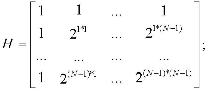

- Internal working processes of the clock
recovery module # 1 and the clockrecovery module # 2 are similar to that inFIG. 4 (b) , and only the chromatic dispersion equalization functions Ih(w) and Qh(w) need to be replaced with functions for equalizing clock delays. A delay caused by a clock is expressed as h(t) = exp(-2πft 0) by using a time-domain finite impulse response. In the clock recovery module, Ih(w) and Qh(w) may be replaced with NTT transformation of cos(2πft 0) . Details are not described herein. -
FIG. 5 is a schematic diagram of still another Rx DSP architecture according to an embodiment of this application. TheRx DSP architecture 500 includes:
a digital back propagation (digital back propagation, DBP)module 510, afirst NTT module 211, aclock recovery module 213, a firstpolarization compensation module 214, afirst INTT module 215, acombination module 216, aphase recovery module 217, and adecoding module 218. - An architecture after the first
polarization compensation module 214 in theRx DSP architecture 500 is the same as that in theRx DSP architecture 200. A difference lies in that a signal undergoes DBP processing before polarization compensation. Because theDBP module 510 has a chromatic dispersion compensation function, a process after the DBP module may not require the chromaticdispersion compensation module 212. - Signals I1 x, Q1 x, I1 y, and Q1 y are input to the
DBP module 510, DBP processing is performed, and time-domain tenth real-number signals Ix_4, Qx_4, Iy_4, and Qy_4 are output to thefirst NTT module 211. - The
first NTT module 211 includes anNTT module # 1, anNTT module # 2, anNTT module # 3, and anNTT module # 4. Ix_4, Qx_4, Iy_4, and Qy_4 are input to theNTT module # 1, theNTT module # 2, theNTT module # 3, and theNTT module # 4 respectively. - The
NTT module # 1, theNTT module # 2, theNTT module # 3, and theNTT module # 4 perform NTT processing on Ix_4, Qx_4, Iy_4, and Qy_4 respectively, and output transform-domain first real-number signals Ix_1, Qx_1, Iy_1, and Qy_1 to theclock recovery module 213. - The
clock recovery module 213 includes a clockrecovery module # 1 and a clockrecovery module # 2. Ix_1 and Qx_1 are input to the clockrecovery module # 1, and clock recovery is performed to obtain transform-domain second real-number signals Ix_2 and Qx_2. Iy_1 and Qy_1 are input to the clockrecovery module # 2, and clock recovery is performed to obtain transform-domain second real-number signals Iy_2 and Qy_2. - For a process after the
clock recovery module 213, refer to the embodiment shown inFIG. 2 . - The
Rx DSP architecture 500 shown inFIG. 5 may be referred to as a full-transform-domain Rx DSP architecture in which DBP is added. A difference from the full-transform-domain Rx DSP architecture shown inFIG. 2 lies in that the DBP module is added. It should be understood that in the full-transform-domain Rx DSP architecture shown inFIG. 2 , only a linear impairment of an optical fiber is compensated for, for example, chromatic dispersion compensation. In the full-transform-domain Rx DSP architecture in which the DBP module is added, the DBP module is used to implement nonlinear-effect compensation on a basis of a linear impairment, to increase a signal transmission distance. -
FIG. 6 is a schematic diagram of still another Rx DSP architecture according to an embodiment of this application. TheRx DSP architecture 600 includes:
aDBP module 510, afirst NTT module 211, aclock recovery module 213, a secondpolarization compensation module 310, acoefficient update module 311, afirst INTT module 215, acombination module 216, aphase recovery module 320, and adecoding module 330. - An architecture after the second
polarization compensation module 310 in theRx DSP architecture 600 is the same as that in theRx DSP architecture 300. An architecture before the secondpolarization compensation module 310 is the same as that in theRx DSP architecture 500. To be specific, a received signal obtained through conversion by an ADC first undergoes DBP processing. For a process before the DBP processing and clock recovery, refer to the embodiment shown inFIG. 5 . For a process after theclock recovery module 213, refer to the embodiment shown inFIG. 3 . - The
Rx DSP architecture 600 shown inFIG. 6 may be referred to as an Rx DSP architecture combining time domain and transform domain in which DBP is added. A difference from the Rx DSP architecture combining time domain and transform domain shown inFIG. 3 lies in that the DBP module is added. It should be understood that in the Rx DSP architecture combining time domain and transform domain shown inFIG. 3 , only a linear impairment of an optical fiber is compensated for, for example, chromatic dispersion compensation. In the Rx DSP architecture combining time domain and transform domain in which the DBP module is added, the DBP module is used to implement nonlinear-effect compensation on a basis of a linear impairment, to increase a signal transmission distance. -
FIG. 7 is a schematic structural diagram of a DBP module according to an embodiment of this application. TheDBP module 700 includes:
asecond NTT module 711, a second chromaticdispersion compensation module 712, asecond INTT module 713, and anonlinear compensation module 714, where a structure of the second chromaticdispersion compensation module 712 is shown inFIG. 4 (b) , and is not described in detail herein. - It can be learned from the structural diagram of the DBP module shown in
FIG. 7 that the performing DBP processing on I1 x, Q1 x, I1 y, and Q1 y to obtain the real-number signals Ix_4, Qx_4, Iy_4, and Qy_4 shown inFIG. 5 andFIG. 6 specifically includes the following steps. - The
second NTT module 711 includes anNTT module # 1, anNTT module # 2, anNTT module # 3, and anNTT module # 4. I1 x, Q1 x, I1 y, and Q1 y are input to theNTT module # 1, theNTT module # 2, theNTT module # 3, and theNTT module # 4 respectively. - The
NTT module # 1, theNTT module # 2, theNTT module # 3, and theNTT module # 4 perform NTT processing on I1 x, Q1 x, I1 y, and Q1 y respectively, and output fourth real-number signals Ix_4', Qx_4', Iy_4', and Qy_4' to the second chromaticdispersion compensation module 712. - The second chromatic
dispersion compensation module 712 includes a chromatic dispersioncompensation module # 1 and a chromatic dispersioncompensation module # 2. Ix_4' and Qx_4' are input to the chromatic dispersioncompensation module # 1, and chromatic dispersion compensation is performed in transform domain to obtain transform-domain fifth real-number signals Ix_4" and Qx_4". Iy_4' and Qy_4' are input to the chromatic dispersioncompensation module # 2, and chromatic dispersion compensation is performed in transform domain to obtain transform-domain fifth real-number signals Iy_4" and Qy_4". - The
second INTT module 713 includes anINTT module # 1, anINTT module # 2, anINTT module # 3, and anINTT module # 4. Ix_4", Qx_4", Iy_4", and Qy_4" are input to theINTT module # 1, theINTT module # 2, theINTT module # 3, and theINTT module # 4 respectively. - The
INTT module # 1, theINTT module # 2, theINTT module # 3, and theINTT module # 4 perform INTT processing on Ix_4", Qx_4", Iy_4", and Qy_4" respectively, and output time-domain ninth real-number signals Ix_4‴, Qx_4‴, Iy_4‴, and Qy_4‴ to thenonlinear compensation module 714. - The
nonlinear compensation module 714 includes a nonlinearcompensation module # 1 and a nonlinearcompensation module # 2. Ix_4' and Qx_4' are input to the nonlinearcompensation module # 1, and nonlinear compensation is performed to obtain Ix_4 and Qx_4. Iy_4' and Qy_4' are input to the nonlinearcompensation module # 2, and nonlinear compensation is performed to obtain Iy_4 and Qy_4. - It should be noted that the foregoing processing procedure in the DBP module needs to be repeated for Ns times. To ensure performance, when a span of a link increases, a quantity Ns of DBP iterations also needs to be increased. Different DBP solutions are not limited herein. Depending on different power consumption required by scenarios, Ns may be set to be equal to a total span of a link, or single-step DBP may be set. In the DBP module in this embodiment of this application, no FFT module or IFFT module is used; instead, the NTT module and the INTT module are used. In this way, during a signal processing procedure of the DBP module, repeated Ns transformations do not cause error accumulation.
-
FIG. 8 (a) is a schematic structural diagram of a firstpolarization compensation module 214 according to an embodiment of this application.FIG. 8 (b) is a schematic structural diagram of a secondpolarization compensation module 310 according to an embodiment of this application. - It can be learned from
FIG. 8 (a) that the firstpolarization compensation module 214 in this embodiment of this application includes abutterfly filter 810 and abutterfly filter 820. Thebutterfly filter 810 includes afilter 801, afilter 802, afilter 803, afilter 804, anadder 805, and anadder 806. Thebutterfly filter 820 includes afilter 807, afilter 808, afilter 809, afilter 8010, anadder 8011, and anadder 8012. - Output of the
filter 801, output of thefilter 807, output of thefilter 803, and output of thefilter 809 are negative. The foregoing four signals are input to theadder 805 to obtain a signal Ix_5 that has undergone chromatic dispersion compensation. The output of thefilter 801, the output of thefilter 807, the output of thefilter 803, and the output of thefilter 809 are input to theadder 805 to obtain a signal Qx_5 that has undergone chromatic dispersion compensation. Output of thefilter 802, output of thefilter 808, output of thefilter 804, and output of thefilter 8010 are negative. The foregoing four signals are input to theadder 806 to obtain a signal Iy_5 that has undergone chromatic dispersion compensation. The output of thefilter 802, the output of thefilter 808, the output of thefilter 804, and the output of thefilter 8010 are output to theadder 805 to obtain a signal Qy_5 that has undergone chromatic dispersion compensation. - A clock recovery module outputs four signals. The four signals Ix_2, Qx_2, Iy_2, and Qy_2 are input to a polarization compensation module. The polarization compensation module includes two butterfly filters. One butterfly filter represents a 2×2 two-input, two-output system. Two complex-number signals are input, and two complex-number signals are output. Because real-number signals are processed in NTT transformation, a polarization equalization part is a 4×4 four-input, four-output system.
- The
first butterfly filter 810 is for equalization and depolarization of I-path signals (including an x-polarization I-path signal Ix_2 and a y-polarization I-path signal Iy_2), and a transformation matrix is
second butterfly filter 820 is for Q-path signals (including an x-polarization Q-path signal Qx_2 and a y-polarization Q-path signal Qy_2), and a transformation matrix is
- The polarization compensation module outputs four real-number signals: Ix_5, Qx_5, Iy_5, and Qy_5. A process of performing polarization compensation by the first
polarization compensation module 214 is described with reference toFIG. 8 (a) . - Input signals of the first
polarization compensation module 214 are four real-number signals: Ix_2, Qx_2, Iy_2, and Qy_2, which are a codirectional signal Ix_2 in a polarization direction x, a quadrature signal Qx_2 in the polarization direction x, a codirectional signal Iy_2 in a polarization direction y, and a quadrature signal Qy_2 in the polarization direction y, respectively. - Specifically, a multiplication result of Ix_2 and Ihxx is input to the
adder 805, a negative value of a multiplication result of Qx_2 and Qhxx is input to theadder 805, a multiplication result of Iy_2 and Ihxy is input to theadder 805, a negative value of a multiplication result of Qy_2 and Qhxy is input to theadder 805, and theadder 805 outputs a codirectional signal Ix_5 that is in the polarization direction x and that is obtained through polarization compensation. - A multiplication result of Ix_2 and Qhxx is input to the
adder 8011, a negative value of a multiplication result of Qx_2 and Ihxx is input to theadder 8011, a multiplication result of Iy_2 and Qhxy is input to theadder 8011, a multiplication result of Qy_2 and Ihxy is input to theadder 8011, and theadder 8011 outputs a quadrature signal Qx_5 that is in the polarization direction x and that is obtained through polarization compensation. - A multiplication result of Ix_2 and Ihyx is input to the
adder 806, a negative value of a multiplication result of Qx_2 and Qhyx is input to theadder 806, a multiplication result of Iy_2 and Ihyy is input to theadder 806, a negative value of a multiplication result of Qy_2 and Qhyy is input to theadder 806, and theadder 806 outputs a codirectional signal Iy_5 that is in the polarization direction y and that is obtained through polarization compensation. - A multiplication result of Ix_2 and Qhyx is input to the
adder 8012, a multiplication result of Qx_2 and Ihyx is input to theadder 8012, a multiplication result of Iy_2 and Qhyy is input to theadder 8012, a multiplication result of Qy_2 and Ihyy is input to theadder 8012, and theadder 8012 outputs a quadrature signal Qy_5 that is in the polarization direction y and that is obtained through polarization compensation. - A process in which the output Ix_5, Qx_5, Iy_5, and Qy_5 of the first
polarization compensation module 214 interact with an equalization matrix and the input signals Ix_2, Qx_2, Iy_2, and Qy_2 is described by using the following formula:
- For example, the first
polarization compensation module 214 further includes a coefficient update module 2141 (not shown in the figure). Thecoefficient update module 2141 is configured to update a coefficient of a filter included in the firstpolarization compensation module 214. In this embodiment of this application, manners of updating equalization coefficient matrices

- It can be learned from
FIG. 8 (b) that the secondpolarization compensation module 310 in this embodiment of this application includes 2×2 butterfly filters, and the butterfly filters include afilter 801, afilter 802, afilter 803, afourth filter 804, anadder 805, and anadder 806. - Functions of the second
polarization compensation module 310 include channel optical fiber effects such as equalization compensation (equalization compensation), a differential group delay (differential group delay, DGD), and residual chromatic dispersion. An optical fiber effect may be described by using a 2×2 impairment matrix. An inverse matrix of the impairment matrix may be obtained by using different algorithms. Tap coefficients of a time-domain butterfly filter 108 are hxx, hxy, hyx, and hyy. X and Y signals are convolved with the tap coefficient matrices hxx, hxy, hyx, and hyy to obtain signals Xout and Yout that have undergone polarization impairment compensation. Common algorithms for calculating a tap coefficient matrix include a constant modulus algorithm (constant modulus algorithm, CMA), a least mean square (Least Mean Square, LMS), and various modified versions of the LMS or other forms such as a data-aided LMS. - The
combination module 216 outputs a complex-number signal X in a polarization direction X, and the complex-number signal X is input to thefilter 801 and thefilter 803. Thecombination module 216 outputs a complex-number signal Y in a polarization direction Y, and the complex-number signal Y is input to thefilter 802 and thefilter 804. Thefilter 801 and thefilter 803 provide output to theadder 805. Thefilter 802 and thefilter 804 provide output to theadder 806. - hxx, hxy, hyx, and hyy in
FIG. 8 (b) represent coefficients of thefilter 801, thefilter 802, thefilter 803, and thefilter 804 respectively. - It should be noted that although
FIG. 8 (a) andFIG. 8 (b) are used as examples to describe the butterfly filters in this application, the butterfly filters shown inFIG. 8 (a) andFIG. 8 (b) are merely examples, and do not constitute any limitation on the protection scope of this application. The butterfly filters in the embodiments of this application should be understood in a broad sense, and a filter or a filter combination that can implement a deconvolution function may be referred to as a butterfly filter. - The Rx DSP provided in this embodiment of this application may be further applied to a multi-mode transmission scenario. For example, the Rx DSP is applied to m transmission modes. In this case, the Rx DSP receives P real-number signals.
-
FIG. 9 (a) is a schematic diagram of an Rx DSP architecture in a multi-mode transmission scenario according to an embodiment of this application. TheRx DSP architecture 900 includes:
afirst NTT module 211, a first chromaticdispersion compensation module 212, aclock recovery module 213, a firstpolarization compensation module 214, afirst INTT module 215, acombination module 216, aphase recovery module 217, and adecoding module 218. - P real-number signals are input to the
first NTT module 211. The first NTT module separately performs NTT processing on the P real-number signals, and outputs P transform-domain first real-number signals to the first chromaticdispersion compensation module 212. - Optionally, the P real-number signals are real-number signals obtained through conversion by an ADC. The P real-number signals include 4×m real-number signals in m transmission modes.
- The first chromatic
dispersion compensation module 212 separately performs chromatic dispersion compensation on the P transform-domain first real-number signals, and outputs P transform-domain third real-number signals to theclock recovery module 213. - The
clock recovery module 213 separately performs clock recovery on the P transform-domain third real-number signals, and outputs P transform-domain second real-number signals to the firstpolarization compensation module 214. - The first
polarization compensation module 214 performs polarization compensation processing on the P transform-domain second real-number signals, and outputs P transform-domain sixth real-number signals to thefirst INTT module 215. - The
first INTT module 215 separately performs INTT processing on the P transform-domain sixth real-number signals, and outputs P time-domain seventh real-number signals to thecombination module 216. - The
combination module 216 combines the P time-domain seventh real-number signals, and outputs m complex-number signals X and m complex-number signals Y to thephase recovery module 217 and thedecoding module 218. - The
phase recovery module 217 and thedecoding module 218 perform phase recovery and decoding processing on the m complex-number signals X and the m complex-number signals Y to obtain recovered bit signals. -
FIG. 9 (b) is a schematic diagram of an Rx DSP architecture in another multi-mode transmission scenario according to an embodiment of this application. TheRx DSP architecture 910 includes:
afirst NTT module 211, a first chromaticdispersion compensation module 212, aclock recovery module 213, a secondpolarization compensation module 108, afirst INTT module 215, acombination module 216, aphase recovery module 320, and adecoding module 330. - Modules before clock recovery in the
architecture 910 are the same as those in thearchitecture 900. A difference lies in that a signal output by the clock recovery module is first processed by the INTT module and combined by the combination module, and then input to the secondpolarization compensation module 108. A process before the clock recovery is not described again. - The
first INTT module 215 separately performs INTT processing on the P transform-domain second real-number signals, and outputs P time-domain eighth real-number signals to thecombination module 216. Thecombination module 216 combines the P time-domain eighth real-number signals, and outputs m complex-number signals X and m complex-number signals Y to the secondpolarization compensation module 310. - The second
polarization compensation module 310 performs polarization compensation processing on the m complex-number signals X and the m complex-number signals Y, and outputs m time-domain complex-number signals X and m time-domain complex-number signals Y obtained through polarization compensation to thephase recovery module 320 and thedecoding module 330. The secondpolarization compensation module 310 further includes a coefficient update module 311 (not shown in the figure). Thecoefficient update module 311 is configured to update a coefficient of a filter included in the secondpolarization compensation module 310. - The
phase recovery module 320 and thedecoding module 330 perform phase recovery and decoding processing on the m complex-number signals X and the m complex-number signals Y to obtain recovered bit signals. -
FIG. 9 (c) is a schematic diagram of an Rx DSP architecture in still another multi-mode transmission scenario according to an embodiment of this application. TheRx DSP architecture 920 includes:
aDBP module 510, afirst NTT module 211, aclock recovery module 213, a firstpolarization compensation module 214, afirst INTT module 215, acombination module 216, aphase recovery module 217, and adecoding module 218. - An architecture after the first
polarization compensation module 214 in theRx DSP architecture 920 is the same as that in theRx DSP architecture 900. A difference lies in that a signal undergoes DBP processing before polarization compensation. Because theDBP module 510 has a chromatic dispersion compensation function, a process after the DBP module may not require the chromaticdispersion compensation module 212. - P real-number signals are input to the
DBP module 510, DBP processing is performed, and P time-domain tenth real-number signals are output to thefirst NTT module 211. - The
first NTT module 211 separately performs NTT processing on the P time-domain tenth real-number signals, and outputs P transform-domain first real-number signals to theclock recovery module 213. - The
clock recovery module 213 separately performs clock recovery processing on the P transform-domain first real-number signals, and outputs P transform-domain second real-number signals to the firstpolarization compensation module 214. - For a process after the
clock recovery module 213, refer to the embodiment shown inFIG. 9 (a) . -
FIG. 9 (d) is a schematic diagram of an Rx DSP architecture in still another multi-mode transmission scenario according to an embodiment of this application. TheRx DSP architecture 930 includes:
aDBP module 510, afirst NTT module 211, aclock recovery module 213, a secondpolarization compensation module 310, afirst INTT module 215, acombination module 216, aphase recovery module 320, and adecoding module 330. - An architecture after the second
polarization compensation module 310 in theRx DSP architecture 930 is the same as that in theRx DSP architecture 910. An architecture before the secondpolarization compensation module 310 is the same as that in theRx DSP architecture 920. To be specific, a received signal obtained through conversion by an ADC first undergoes DBP processing. For a process before the DBP processing and clock recovery, refer to the embodiment shown inFIG. 9 (c) . For a process after theclock recovery module 213, refer to the embodiment shown inFIG. 9 (b) . - For example, the
DBP module 510 shown inFIG. 9 (c) andFIG. 9 (d) is shown inFIG. 9 (e). FIG. 9 (e) is a schematic structural diagram of another DBP module according to an embodiment of this application. TheDBP module 940 includes:
asecond NTT module 711, a second chromaticdispersion compensation module 712, asecond INTT module 713, and anonlinear compensation module 714. - That P real-number signals are input to the
DBP module 510, and DBP processing is performed to obtain P time-domain tenth real-number signals specifically includes the following steps. - The P real-number signals are respectively input to P
second NTT modules 711, NTT processing is performed, and P transform-domain fourth real-number signals are output to the second chromaticdispersion compensation module 712. - The second chromatic
dispersion compensation module 712 performs chromatic dispersion compensation processing on the P transform-domain fourth real-number signals, and outputs P transform-domain fifth real-number signals to thesecond INTT module 713. - The
second INTT module 713 performs INTT processing on the P transform-domain fifth real-number signals, and outputs P time-domain ninth real-number signals to thenonlinear compensation module 714. - The
nonlinear compensation module 714 performs nonlinear compensation on the P time-domain ninth real-number signals to obtain the P time-domain tenth real-number signals. - Specifically, compared with performing signal processing by using the FFT module and the IFFT module, performing signal processing by using the NTT module and the INTT module has the following advantages.
- (1) When signal processing is performed based on the NTT module and the INTT module, complexity of the Rx DSP architecture is reduced.
- When signal processing is performed based on the FFT module and the IFFT module, during a signal transmission process, power consumption of merely chromatic dispersion compensation accounts for half of total power consumption of Rx DSP, and complexity of N-point FFT is proportional to Nlog2N multiplications. Depending on different data bit widths of operations, complexity of a multiplication is equal to several times to dozens of times of that of an addition.
- However, complexity of signal processing performed based on the NTT module and the INTT module is proportional to 2Nlog2N additions. Depending on different data bit widths and different quantities N of transformation points, complexity of signal processing performed based on the NTT module and the INTT module is reduced to different degrees. For example, if a quantity of transformation points is 256, power consumption of NTT is reduced to approximately 1/4 of that of FFT.
- (2) When signal processing is performed based on the NTT module and the INTT module, a transformation matrix has no truncation error or fixed-point penalty.
- When signal processing is performed based on the FFT module and the IFFT module, because a transformation core of FFT is an exponential function, a truncation error cannot be accurately expressed on a binary computer. In addition, a bit width of a transformation matrix is not fixed, causing a fixed-point penalty.
- However, in signal processing performed based on the NTT module and the INTT module, because a transformation core of NTT is an integer and the transformation core is usually 2 or a power of 2, the transformation core can be accurately expressed in a memory. In addition, a bit width of a transformation matrix is fixed, without a fixed-point penalty.
- (3) When signal processing is performed based on the NTT module and the INTT module, no error accumulates.
- A truncation error and a fixed-point penalty in a single FFT or IFFT transformation repeatedly accumulate during DBP propagation. As a result, a final result error is larger.
- However, there is no truncation error or fixed-point penalty in a single NTT or INTT transformation. Therefore, repeated Ns transformations do not cause error accumulation.
- (4) When signal processing is performed based on the NTT module and the INTT module, storage can be reduced.
- A transformation core of NTT is 2, and a transformation matrix includes 2 or a power of 2. In a binary system, a number is multiplied by a power of 2 only through shifting. Therefore, no huge transformation matrix needs to be stored in a DSP process, and only the transformation core needs to be stored.
-
FIG. 10 (a) is a schematic flowchart of a signal processing method according to an embodiment of this application. The following steps S1010 to S1050 are included. - S1010. Obtain P real-number signals.
- For example, the P real-number signals include real-number signals that are in two polarization directions and that correspond to each of m modes. When m is equal to 1, it indicates single-mode transmission; or when m is greater than 1, it indicates multi-mode transmission. m and P are positive integers.
- S1020. Obtain P transform-domain first real-number signals.
- At least NTT processing is performed on the P real-number signals to obtain the P transform-domain first real-number signals. The following two possible implementations are included.
- Implementation 1.1: Perform NTT processing on the P real-number signals to obtain the P transform-domain first real-number signals.
- Implementation 1.2: Sequentially perform DBP processing and NTT processing on the P real-number signals to obtain the P transform-domain first real-number signals.
- In the implementation 1.2, DBP processing is first performed on the P real-number signals to obtain P time-domain tenth real-number signals, and then NTT processing is performed on the P time-domain tenth real-number signals to obtain the P transform-domain first real-number signals.
- The performing NTT processing on the P real-number signals in the implementation 1.1, and the performing NTT processing on the P time-domain tenth real-number signals that are obtained by performing DBP processing on the P real-number signals in the implementation 1.2 may be collectively referred to as performing NTT processing on P input signals. In other words, in this embodiment of this application, the P input signals include the P real-number signals, or the P time-domain tenth real-number signals that are obtained by performing DBP processing on the P real-number signals.
- For ease of understanding, a process of performing DBP processing on the P real-number signals to obtain the P time-domain tenth real-number signals is briefly described with reference to
FIG. 10 (b). FIG. 10 (b) is a schematic flowchart of DBP processing according to an embodiment of this application. The following steps S1021 to S1024 are included. - S1021. Obtain P transform-domain fourth real-number signals.
- NTT processing is performed on P real-number signals to obtain the P transform-domain fourth real-number signals.
- S1022. Obtain P transform-domain fifth real-number signals.
- Chromatic dispersion compensation is performed on the P transform-domain fourth real-number signals in transform domain to obtain the P transform-domain fifth real-number signals.
- S1023. Obtain P time-domain ninth real-number signals.
- INTT processing is performed on the P transform-domain fifth real-number signals to obtain the P time-domain ninth real-number signals.
- S1024. Obtain P time-domain tenth real-number signals.
- Nonlinear compensation is performed on the P time-domain ninth real-number signals to obtain the P time-domain tenth real-number signals.
- S1030. Obtain P transform-domain second real-number signals.
- At least clock recovery processing is performed on the P transform-domain first real-number signals to obtain the P transform-domain second real-number signals. Corresponding to the two possibilities in step S1020, the following two possible implementations are included.
- Implementation 2.1: This corresponds to the implementation 1.1 in step S1020. A processing procedure includes the following steps.
- First, perform chromatic dispersion compensation on the P transform-domain first real-number signals to obtain P transform-domain third real-number signals.
- Then, separately perform clock recovery on the P transform-domain third real-number signals to obtain the P transform-domain second real-number signals.
- The performing chromatic dispersion compensation on the P transform-domain first real-number signals to obtain P transform-domain third real-number signals specifically includes the following steps:
- First, determine a chromatic dispersion impulse response Ih(t) corresponding to an in-phase real-number signal and a chromatic dispersion impulse response Qh(t) corresponding to a quadrature real-number signal, and perform NTT to obtain a transform-domain chromatic dispersion equalization function Ih(w) corresponding to the in-phase real-number signal and a transform-domain chromatic dispersion equalization function Qh(w) corresponding to the quadrature real-number signal.
- Then, determine 2×m transform-domain third real-number signals that are in the P transform-domain third real-number signals and that are in a first polarization direction based on Ih(w), Qh(w), and an in-phase real-number signal and a quadrature real-number signal that are in the P transform-domain first real-number signals and that are in the first polarization direction, and determine 2×m transform-domain third real-number signals that are in the P transform-domain third real-number signals and that are in a second polarization direction based on Ih(w), Qh(w), and an in-phase real-number signal and a quadrature real-number signal that are in the P transform-domain first real-number signals and that are in the second polarization direction.
- Specifically, the transform-domain third real-number signals obtained through chromatic dispersion compensation and the transform-domain first real-number signals that have not undergone chromatic dispersion compensation meet the following requirements:



Ix(w) represents an in-phase real-number signal that is in the transform-domain first real-number signals and that is in the first polarization direction, Qx(w) represents a quadrature real-number signal that is in the transform-domain first real-number signals and that is in the first polarization direction, Iy(w) represents an in-phase real-number signal that is in the transform-domain first real-number signals and that is in the second polarization direction, Qy(w) represents a quadrature real-number signal that is in the transform-domain first real-number signals and that is in the second polarization direction, I'x(w) represents an in-phase real-number signal that is in the transform-domain third real-number signals and that is in the first polarization direction, Q'x(w) represents a quadrature real-number signal that is in the transform-domain third real-number signals and that is in the first polarization direction, I'y(w) represents an in-phase real-number signal that is in the transform-domain third real-number signals and that is in the second polarization direction, and Q'y(w) represents a quadrature real-number signal that is in the transform-domain third real-number signals and that is in the second polarization direction. - This corresponds to the implementation 1.2 in step S1020. A processing procedure includes the following step:
Separately perform clock recovery on the P transform-domain first real-number signals to obtain the P transform-domain second real-number signals. - S1040. Obtain time-domain complex-number signals.
- At least polarization compensation processing and INTT processing are performed on the P transform-domain second real-number signals to obtain m time-domain complex-number signals X and m time-domain complex-number signals Y. The following two possible implementations are included.
- Implementation 3.1: Sequentially perform polarization compensation processing, INTT processing, and combination processing on the P transform-domain second real-number signals to obtain the m time-domain complex-number signals X and the m time-domain complex-number signals Y.
FIG. 10 (c) is a schematic flowchart of obtaining a time-domain complex-number signal according to an embodiment of this application. The following steps S1041 to S1043 are included. - S1041. Obtain P transform-domain sixth real-number signals.
- Polarization compensation is performed on P transform-domain second real-number signals to obtain the P transform-domain sixth real-number signals.
- S1042. Obtain P time-domain seventh real-number signals.
- INTT processing is separately performed on the P transform-domain sixth real-number signals to obtain the P time-domain seventh real-number signals.
- S1043. Perform combination to obtain m complex-number signals X and m complex-number signals Y.
- Every two of 2×m time-domain seventh real-number signals that are in the P time-domain seventh real-number signals and that are in a first polarization direction are combined to obtain the m time-domain complex-number signals X in the first polarization direction.
- Every two of 2×m time-domain seventh real-number signals that are in the P time-domain seventh real-number signals and that are in a second polarization direction are combined to obtain the m time-domain complex-number signals Y in the second polarization direction.
- Implementation 3.2: Sequentially perform INTT processing, combination processing, and polarization compensation processing on the P transform-domain second real-number signals.
FIG. 10 (d) is another schematic flowchart of obtaining a time-domain complex-number signal according to an embodiment of this application. The following steps S1044 to S1046 are included. - S1044. Obtain P time-domain eighth real-number signals.
- INTT processing is performed on P transform-domain second real-number signals to obtain the P time-domain eighth real-number signals.
- S1045. Obtain m complex-number signals X and m complex-number signals Y.
- Every two of 2×m time-domain eighth real-number signals that are in the P time-domain eighth real-number signals and that are in a first polarization direction are combined to obtain the m time-domain complex-number signals X in the first polarization direction.
- Every two of 2×m time-domain eighth real-number signals that are in the P time-domain eighth real-number signals and that are in a second polarization direction are combined to obtain the m time-domain complex-number signals Y in the second polarization direction.
- S1046. Obtain m complex-number signals X and m complex-number signals Y that have undergone polarization compensation.
- Polarization compensation is performed on the m time-domain complex-number signals X in the first polarization direction and the m time-domain complex-number signals Y in the second polarization direction to obtain the m time-domain complex-number signals X and the m time-domain complex-number signals Y that have undergone the polarization compensation.
- S1050. Obtain bit signals.
- To obtain the recovered bit signals, phase recovery and decoding need to be performed on the time-domain complex-number signals obtained in S1040.
- First, phase recovery is performed on the m time-domain complex-number signals X and the m time-domain complex-number signals Y to obtain m time-domain complex-number signals X and m time-domain complex-number signals Y that have undergone the phase recovery.
- Then, the m time-domain complex-number signals X and the m time-domain complex-number signals Y that are obtained through phase recovery are decoded to obtain m time-domain complex-number signals X and m time-domain complex-number signals Y that have been decoded.
- It should be noted that how to perform phase recovery and decoding on the time-domain complex-number signals is not limited in this embodiment of this application. Refer to a current process of performing phase recovery and decoding on an electrical signal by a polarization multiplexing coherent receiver.
- An embodiment of this application further provides a coherent receiver, including a polarization beam splitter, a frequency mixer, a photoelectric detector, an analog-to-digital converter, and the Rx DSP shown in
FIG. 9 (a) ,FIG. 9 (b) ,FIG. 9 (c) , orFIG. 9 (d) . The polarization beam splitter, the frequency mixer, the photoelectric detector, and the analog-to-digital converter are similar to those shown inFIG. 1 (a) andFIG. 1 (b) . Details are not described herein again. - An embodiment of this application further provides a chip.
FIG. 11 is a schematic diagram of achip 1100 according to this application. Thechip 1100 includes aprocessor 1110, amemory 1120, and acommunications interface 1130. Theprocessor 1110 is coupled to thememory 1120. Thememory 1120 is configured to store a computer program or an instruction and/or data. Theprocessor 1110 is configured to execute the computer program or the instruction and/or the data stored in thememory 1120, so that the method in the foregoing method embodiment is performed. - In a possible implementation, the chip shown in
FIG. 11 may be a signal processing apparatus including aprocessor 1110 and acommunications interface 1130. Theprocessor 1110 is coupled to a memory by using thecommunications interface 1130, and theprocessor 1110 is configured to perform the method in the foregoing method embodiment. - It should be understood that the foregoing embodiments are merely examples for describing the signal processing procedure provided in this application, and do not constitute any limitation on the protection scope of this application. Other simple variations of the Rx DSP architecture all fall within the protection scope of this application. A difference between the Rx DSP architecture in this application and an existing Rx DSP architecture lies in that an FFT module and an IFFT module are not used for signal processing, but an NTT module and an INTT module are used.
- It should be further understood that, in the embodiments of this application, unless otherwise specified or in case of a logical conflict, terms and/or descriptions in different embodiments may be consistent and may be mutually referenced. Technical features in different embodiments may be combined based on an internal logical relationship of the technical features to form a new embodiment.
- It may be clearly understood by a person skilled in the art that, for the purpose of convenient and brief description, for a detailed working process of the foregoing system, apparatus, and unit, refer to a corresponding process in the foregoing method embodiments, and details are not described herein again.
- When the functions are implemented in the form of a software functional unit and sold or used as an independent product, the functions may be stored in a computer-readable storage medium. Based on such an understanding, the technical solutions of this application essentially, or the part contributing to the prior art, or some of the technical solutions may be implemented in a form of a software product. The software product is stored in a storage medium, and includes several instructions for instructing a computer device (which may be a personal computer, a server, or a network device) to perform all or some of the steps of the methods described in the embodiments of this application. The foregoing storage medium includes: any medium that can store program code, such as a USB flash drive, a removable hard disk, a read-only memory (read-only memory, ROM), a random access memory (random access memory, RAM), a magnetic disk, or an optical disc.
Claims (14)
- A signal processing method, wherein the method comprises:obtaining P real-number signals;performing at least number theoretic transform NTT processing on the P real-number signals to obtain P transform-domain first real-number signals;performing at least clock recovery on the P transform-domain first real-number signals to obtain P transform-domain second real-number signals;performing at least polarization compensation and inverse number theoretic transform INTT processing on the P transform-domain second real-number signals to obtain m time-domain complex-number signals X and m time-domain complex-number signals Y; andperforming phase recovery and decoding on the m time-domain complex-number signals X and the m time-domain complex-number signals Y to obtain bit signals, whereinm and P are positive integers.
- The method according to claim 1, wherein the P real-number signals comprise 4×m real-number signals in m transmission modes, and when m is equal to 1, it indicates single-mode transmission, or when m is greater than 1, it indicates multi-mode transmission.
- The method according to claim 1 or 2, wherein the performing at least clock recovery on the P transform-domain first real-number signals to obtain P transform-domain second real-number signals comprises:performing chromatic dispersion compensation on the P transform-domain first real-number signals to obtain P transform-domain third real-number signals; andperforming clock recovery on the P transform-domain third real-number signals to obtain the P transform-domain second real-number signals.
- The method according to claim 3, wherein the P real-number signals comprise an in-phase real-number signal Im x and a quadrature real-number signal Qm x in a first polarization direction, and an in-phase real-number signal Im y and a quadrature real-number signal Qm y in a second polarization direction; and
the performing chromatic dispersion compensation on the P transform-domain first real-number signals to obtain the P transform-domain third real-number signals comprises:performing NTT processing on a chromatic dispersion impulse response Ih(t) corresponding to an in-phase real-number signal and a chromatic dispersion impulse response Qh(t) corresponding to a quadrature real-number signal, to obtain a transform-domain chromatic dispersion equalization function Ih(w) corresponding to the in-phase real-number signal and a transform-domain chromatic dispersion equalization function Qh(w) corresponding to the quadrature real-number signal;determining 2×m transform-domain third real-number signals that are in the P transform-domain third real-number signals and that are in the first polarization direction based on Ih(w), Qh(w), and an in-phase real-number signal Ix(w) and a quadrature real-number signal Qx(w) that are in the P transform-domain first real-number signals and that are in the first polarization direction; anddetermining 2×m transform-domain third real-number signals that are in the P transform-domain third real-number signals and that are in the second polarization direction based on Ih(w), Qh(w), and an in-phase real-number signal Iy(w) and a quadrature real-number signal Qy(w) that are in the P transform-domain first real-number signals and that are in the second polarization direction. - The method according to claim 4, wherein the transform-domain third real-number signals obtained through chromatic dispersion compensation and the transform-domain first real-number signals meet the following requirements:


Ix(w) represents an in-phase real-number signal that is in the transform-domain first real-number signals and that is in the first polarization direction, Qx(w) represents a quadrature real-number signal that is in the transform-domain first real-number signals and that is in the first polarization direction, Iy(w) represents an in-phase real-number signal that is in the transform-domain first real-number signals and that is in the second polarization direction, Qy(w) represents a quadrature real-number signal that is in the transform-domain first real-number signals and that is in the second polarization direction, I'x(w) represents an in-phase real-number signal that is in the transform-domain third real-number signals and that is in the first polarization direction, Q'x(w) represents a quadrature real-number signal that is in the transform-domain third real-number signals and that is in the first polarization direction, I'y(w) represents an in-phase real-number signal that is in the transform-domain third real-number signals and that is in the second polarization direction, and Q'y(w) represents a quadrature real-number signal that is in the transform-domain third real-number signals and that is in the second polarization direction. - The method according to claim 1, wherein the performing at least number theoretic transform NTT processing on the P real-number signals to obtain P transform-domain first real-number signals comprises:performing digital back propagation DBP processing on the P real-number signals to obtain P time-domain tenth real-number signals; andseparately performing NTT processing on the P time-domain tenth real-number signals to obtain the P transform-domain first real-number signals.
- The method according to claim 6, wherein the performing DBP processing on the P real-number signals to obtain P time-domain tenth real-number signals comprises:performing NTT processing on the P real-number signals to obtain P transform-domain fourth real-number signals;performing, in transform domain, chromatic dispersion compensation on the P transform-domain fourth real-number signals to obtain P transform-domain fifth real-number signals;performing INTT processing on the P transform-domain fifth real-number signals to obtain P time-domain ninth real-number signals; andperforming nonlinear compensation on the P time-domain ninth real-number signals to obtain the P time-domain tenth real-number signals.
- The method according to any one of claims 1 to 7, wherein the performing at least polarization compensation and inverse number theoretic transform INTT processing on the P transform-domain second real-number signals to obtain m time-domain complex-number signals X and m time-domain complex-number signals Y comprises:performing polarization compensation on the P transform-domain second real-number signals to obtain P transform-domain sixth real-number signals;performing INTT processing on the P transform-domain sixth real-number signals to obtain P time-domain seventh real-number signals; andcombining every two of 2×m time-domain seventh real-number signals that are in the P time-domain seventh real-number signals and that are in the first polarization direction to obtain m time-domain complex-number signals X in the first polarization direction, and combining every two of 2×m time-domain seventh real-number signals that are in the P time-domain seventh real-number signals and that are in the second polarization direction to obtain m time-domain complex-number signals Y in the second polarization direction.
- The method according to claim 8, wherein the performing polarization compensation on the P transform-domain second real-number signals to obtain P transform-domain sixth real-number signals comprises:performing equalization and depolarization on 2×m transform-domain second real-number signals that are in the P transform-domain second real-number signals and that are in the first polarization direction to obtain 2×m transform-domain sixth real-number signals that are in the P transform-domain sixth real-number signals and that are in the first polarization direction; andperforming equalization and depolarization on 2×m transform-domain second real-number signals that are in the P transform-domain second real-number signals and that are in the second polarization direction to obtain 2×m transform-domain sixth real-number signals that are in the P transform-domain sixth real-number signals and that are in the second polarization direction.
- The method according to any one of claims 1 to 7, wherein the performing at least polarization compensation and inverse number theoretic transform INTT processing on the P transform-domain second real-number signals to obtain m time-domain complex-number signals X and m time-domain complex-number signals Y comprises:performing INTT processing on the P transform-domain second real-number signals to obtain P time-domain eighth real-number signals;combining every two of 2×m time-domain eighth real-number signals that are in the P time-domain eighth real-number signals and that are in the first polarization direction to obtain m time-domain complex-number signals X in the first polarization direction, and combining every two of 2×m time-domain eighth real-number signals that are in the P time-domain eighth real-number signals and that are in the second polarization direction to obtain m time-domain complex-number signals Y in the second polarization direction; andperforming time-domain polarization compensation on the m time-domain complex-number signals X in the first polarization direction and the m time-domain complex-number signals Y in the second polarization direction to obtain m time-domain complex-number signals X and m time-domain complex-number signals Y that have undergone the polarization compensation.
- A signal processing apparatus, comprising:a processor and a communications interface, whereinthe processor is coupled to a memory by using the communications interface, and the processor is configured to execute program code in the memory, to implement the method according to any one of claims 1 to 10.
- A computer-readable storage medium, comprising:the computer-readable storage medium stores a computer program; andwhen the computer program runs on a computer, the computer is enabled to perform the method according to any one of claims 1 to 10.
- A coherent receiver, comprising:
the signal processing apparatus according to claim 11, a polarization beam splitter, a frequency mixer, a photoelectric detector, and an analog-to-digital converter, wherein the polarization beam splitter is configured to obtain signals in two polarization directions, the frequency mixer is configured to perform frequency mixing processing on signals in a same polarization direction among the signals in the two polarization directions that are output by the polarization beam splitter, the photoelectric detector is configured to convert strength of an optical signal output by the frequency mixer into strength of an electrical signal, and the analog-to-digital converter is configured to perform analog-to-digital conversion on a signal output by the photoelectric detector. - A chip, comprising a communications interface, a memory, and a processor, wherein the memory is configured to store a computer program, and the processor is configured to read and execute the computer program stored in the memory, so that the chip implements the method according to any one of claims 1 to 10.
Applications Claiming Priority (2)
| Application Number | Priority Date | Filing Date | Title |
|---|---|---|---|
| RU2020117812A RU2816843C2 (en) | 2020-05-29 | Signal processing method and device and coherent receiver | |
| PCT/CN2021/094742 WO2021238749A1 (en) | 2020-05-29 | 2021-05-20 | Signal processing method and apparatus, and coherent receiver |
Publications (3)
| Publication Number | Publication Date |
|---|---|
| EP4150794A1 EP4150794A1 (en) | 2023-03-22 |
| EP4150794A4 EP4150794A4 (en) | 2023-11-08 |
| EP4150794B1 true EP4150794B1 (en) | 2025-01-29 |
Family
ID=78745563
Family Applications (1)
| Application Number | Title | Priority Date | Filing Date |
|---|---|---|---|
| EP21813281.9A Active EP4150794B1 (en) | 2020-05-29 | 2021-05-20 | Signal processing method and apparatus, and coherent receiver |
Country Status (5)
| Country | Link |
|---|---|
| US (1) | US12081275B2 (en) |
| EP (1) | EP4150794B1 (en) |
| JP (1) | JP7538891B2 (en) |
| CN (1) | CN115606118B (en) |
| WO (1) | WO2021238749A1 (en) |
Family Cites Families (18)
| Publication number | Priority date | Publication date | Assignee | Title |
|---|---|---|---|---|
| FR2570853B1 (en) | 1984-09-24 | 1987-01-02 | Duhamel Pierre | DEVICE FOR REAL-TIME PROCESSING OF DIGITAL SIGNALS BY CONVOLUTION |
| US5179529A (en) * | 1989-03-31 | 1993-01-12 | Hughes Aircraft Company | High speed fourier transform engine |
| CA2011476C (en) * | 1989-03-31 | 1995-02-07 | Michael V. Nowakowski | Fourier transform engine using number theoretic transforms |
| US6625629B1 (en) | 2000-05-23 | 2003-09-23 | Microsoft Corporation | System and method for signal processing using an improved convolution technique |
| US10195464B2 (en) | 2004-06-24 | 2019-02-05 | Varian Medical Systems, Inc. | Systems and methods for treating a lung of a patient using guided radiation therapy or surgery |
| US8005368B2 (en) * | 2007-12-05 | 2011-08-23 | Ciena Corporation | Signal equalizer in a coherent optical receiver |
| ES2673994T3 (en) * | 2009-06-17 | 2018-06-26 | Huawei Technologies Co., Ltd. | Intradine coherent optical receiver |
| CA2766492C (en) * | 2010-02-20 | 2016-04-12 | Huawei Technologies Co., Ltd. | Clock phase recovery apparatus |
| WO2012105714A1 (en) | 2011-02-02 | 2012-08-09 | 日本電気株式会社 | Optical receiver and method for optical reception |
| WO2012109871A1 (en) * | 2011-08-01 | 2012-08-23 | 华为技术有限公司 | Coherent receiver device and chromatic dispersion compensation method |
| EP2660984B1 (en) * | 2011-12-01 | 2016-03-23 | Huawei Technologies Co., Ltd. | Optical signal compensation device |
| US9225431B1 (en) * | 2012-06-19 | 2015-12-29 | Juniper Networks, Inc. | Fast chromatic dispersion estimation |
| CN103713194B (en) * | 2012-10-08 | 2016-08-03 | 富士通株式会社 | A kind of method for detecting phases for clock recovery and device |
| CN103870438B (en) | 2014-02-25 | 2016-08-17 | 复旦大学 | A kind of circuit structure utilizing number theoretic transform to calculate cyclic convolution |
| US10171177B2 (en) | 2014-12-22 | 2019-01-01 | Nec Corporation | Digital signal processor, digital optical receiver using the same, and digital signal processing method |
| JP2017038103A (en) * | 2015-08-06 | 2017-02-16 | 日本電信電話株式会社 | Digital coherent receiver |
| CN106685663B (en) | 2017-02-15 | 2019-07-19 | 华中科技大学 | The encryption method and circuit of error problem concerning study in a kind of annulus |
| KR101952547B1 (en) | 2018-11-23 | 2019-02-26 | 인하대학교 산학협력단 | Method and Apparatus for Number Theoretic Transform based Polynomial Multiplier For Lattice based Cryptosystem |
-
2021
- 2021-05-20 CN CN202180035579.3A patent/CN115606118B/en active Active
- 2021-05-20 JP JP2022573532A patent/JP7538891B2/en active Active
- 2021-05-20 WO PCT/CN2021/094742 patent/WO2021238749A1/en not_active Ceased
- 2021-05-20 EP EP21813281.9A patent/EP4150794B1/en active Active
-
2022
- 2022-11-29 US US18/071,402 patent/US12081275B2/en active Active
Also Published As
| Publication number | Publication date |
|---|---|
| CN115606118A (en) | 2023-01-13 |
| EP4150794A4 (en) | 2023-11-08 |
| US12081275B2 (en) | 2024-09-03 |
| JP7538891B2 (en) | 2024-08-22 |
| RU2020117812A (en) | 2021-12-01 |
| WO2021238749A1 (en) | 2021-12-02 |
| JP2023527233A (en) | 2023-06-27 |
| EP4150794A1 (en) | 2023-03-22 |
| US20230163857A1 (en) | 2023-05-25 |
| CN115606118B (en) | 2025-08-22 |
Similar Documents
| Publication | Publication Date | Title |
|---|---|---|
| Redyuk et al. | Compensation of nonlinear impairments using inverse perturbation theory with reduced complexity | |
| US9515742B2 (en) | System and methods for adaptive equalization for optical modulation formats | |
| Beppu et al. | Weakly coupled 10-mode-division multiplexed transmission over 48-km few-mode fibers with real-time coherent MIMO receivers | |
| Czegledi et al. | Digital backpropagation accounting for polarization-mode dispersion | |
| Secondini et al. | Single-step digital backpropagation for nonlinearity mitigation | |
| EP2660984B1 (en) | Optical signal compensation device | |
| US9369213B1 (en) | Demultiplexing processing for a receiver | |
| US20200366380A1 (en) | Method and apparatus for nonlinear compensation in coherent optical links | |
| US20180123700A1 (en) | Method and apparatus for estimating polarization dependent loss and receiving device | |
| US8884649B1 (en) | System and method for stationary finite impulse response filters in programmable microelectronic circuits | |
| Arikawa et al. | Frequency-domain adaptive MIMO filter with fractional oversampling using stochastic gradient descent for long-haul transmission over coupled 4-core fibers | |
| Liu et al. | Low hardware-complexity IQ skew tolerant finite field and time domain hybrid adaptive equalization for 400G/800G-ZR coherent transmission | |
| Gan et al. | Efficient channel model for homogeneous weakly coupled multicore fibers | |
| US10903911B2 (en) | Apparatus and method for estimating polarization skew | |
| US12081275B2 (en) | Signal processing method and apparatus, and coherent receiver | |
| CN110943785A (en) | Two-stage equalizer and implementation method | |
| Li et al. | The role of effective area in the design of weakly coupled MCF: Optimization guidance and OSNR improvement | |
| RU2816843C2 (en) | Signal processing method and device and coherent receiver | |
| Zhou et al. | Null space method for tap value initialization in constant modulus algorithm for mode division multiplexing systems | |
| Cao et al. | Recombinant real-Björck sequences assisted frequency-domain MIMO scheme for multi-impairment compensation in self-homodyne MDM system | |
| Ma et al. | Digital subcarrier multiplexing-enabled carrier-free phase-retrieval receiver | |
| Muga et al. | PMD tolerance in Stokes space based polarization de-multiplexing algorithms | |
| Gustafsson et al. | Shift-and-add realization trade-offs for chromatic dispersion compensation FIR filters | |
| Liu et al. | Parallel implementation of hardware-efficient adaptive equalization for coherent PON systems | |
| Xing et al. | Study of efficient photonic chromatic dispersion equalization using MZI-based coherent optical matrix multiplication |
Legal Events
| Date | Code | Title | Description |
|---|---|---|---|
| STAA | Information on the status of an ep patent application or granted ep patent |
Free format text: STATUS: THE INTERNATIONAL PUBLICATION HAS BEEN MADE |
|
| PUAI | Public reference made under article 153(3) epc to a published international application that has entered the european phase |
Free format text: ORIGINAL CODE: 0009012 |
|
| STAA | Information on the status of an ep patent application or granted ep patent |
Free format text: STATUS: REQUEST FOR EXAMINATION WAS MADE |
|
| 17P | Request for examination filed |
Effective date: 20221212 |
|
| AK | Designated contracting states |
Kind code of ref document: A1 Designated state(s): AL AT BE BG CH CY CZ DE DK EE ES FI FR GB GR HR HU IE IS IT LI LT LU LV MC MK MT NL NO PL PT RO RS SE SI SK SM TR |
|
| DAV | Request for validation of the european patent (deleted) | ||
| DAX | Request for extension of the european patent (deleted) | ||
| A4 | Supplementary search report drawn up and despatched |
Effective date: 20231011 |
|
| RIC1 | Information provided on ipc code assigned before grant |
Ipc: H04B 10/61 20130101ALI20231005BHEP Ipc: H04B 10/2507 20130101ALI20231005BHEP Ipc: H04B 10/25 20130101AFI20231005BHEP |
|
| GRAP | Despatch of communication of intention to grant a patent |
Free format text: ORIGINAL CODE: EPIDOSNIGR1 |
|
| STAA | Information on the status of an ep patent application or granted ep patent |
Free format text: STATUS: GRANT OF PATENT IS INTENDED |
|
| INTG | Intention to grant announced |
Effective date: 20240913 |
|
| GRAS | Grant fee paid |
Free format text: ORIGINAL CODE: EPIDOSNIGR3 |
|
| GRAA | (expected) grant |
Free format text: ORIGINAL CODE: 0009210 |
|
| STAA | Information on the status of an ep patent application or granted ep patent |
Free format text: STATUS: THE PATENT HAS BEEN GRANTED |
|
| AK | Designated contracting states |
Kind code of ref document: B1 Designated state(s): AL AT BE BG CH CY CZ DE DK EE ES FI FR GB GR HR HU IE IS IT LI LT LU LV MC MK MT NL NO PL PT RO RS SE SI SK SM TR |
|
| REG | Reference to a national code |
Ref country code: GB Ref legal event code: FG4D |
|
| REG | Reference to a national code |
Ref country code: CH Ref legal event code: EP |
|
| REG | Reference to a national code |
Ref country code: DE Ref legal event code: R096 Ref document number: 602021025548 Country of ref document: DE |
|
| REG | Reference to a national code |
Ref country code: IE Ref legal event code: FG4D |
|
| REG | Reference to a national code |
Ref country code: NL Ref legal event code: MP Effective date: 20250129 |
|
| PG25 | Lapsed in a contracting state [announced via postgrant information from national office to epo] |
Ref country code: NL Free format text: LAPSE BECAUSE OF FAILURE TO SUBMIT A TRANSLATION OF THE DESCRIPTION OR TO PAY THE FEE WITHIN THE PRESCRIBED TIME-LIMIT Effective date: 20250129 |
|
| PG25 | Lapsed in a contracting state [announced via postgrant information from national office to epo] |
Ref country code: RS Free format text: LAPSE BECAUSE OF FAILURE TO SUBMIT A TRANSLATION OF THE DESCRIPTION OR TO PAY THE FEE WITHIN THE PRESCRIBED TIME-LIMIT Effective date: 20250429 |
|
| PG25 | Lapsed in a contracting state [announced via postgrant information from national office to epo] |
Ref country code: FI Free format text: LAPSE BECAUSE OF FAILURE TO SUBMIT A TRANSLATION OF THE DESCRIPTION OR TO PAY THE FEE WITHIN THE PRESCRIBED TIME-LIMIT Effective date: 20250129 |
|
| PG25 | Lapsed in a contracting state [announced via postgrant information from national office to epo] |
Ref country code: PL Free format text: LAPSE BECAUSE OF FAILURE TO SUBMIT A TRANSLATION OF THE DESCRIPTION OR TO PAY THE FEE WITHIN THE PRESCRIBED TIME-LIMIT Effective date: 20250129 |
|
| PG25 | Lapsed in a contracting state [announced via postgrant information from national office to epo] |
Ref country code: ES Free format text: LAPSE BECAUSE OF FAILURE TO SUBMIT A TRANSLATION OF THE DESCRIPTION OR TO PAY THE FEE WITHIN THE PRESCRIBED TIME-LIMIT Effective date: 20250129 |
|
| REG | Reference to a national code |
Ref country code: LT Ref legal event code: MG9D |
|
| PG25 | Lapsed in a contracting state [announced via postgrant information from national office to epo] |
Ref country code: NO Free format text: LAPSE BECAUSE OF FAILURE TO SUBMIT A TRANSLATION OF THE DESCRIPTION OR TO PAY THE FEE WITHIN THE PRESCRIBED TIME-LIMIT Effective date: 20250429 Ref country code: IS Free format text: LAPSE BECAUSE OF FAILURE TO SUBMIT A TRANSLATION OF THE DESCRIPTION OR TO PAY THE FEE WITHIN THE PRESCRIBED TIME-LIMIT Effective date: 20250529 |
|
| REG | Reference to a national code |
Ref country code: AT Ref legal event code: MK05 Ref document number: 1764493 Country of ref document: AT Kind code of ref document: T Effective date: 20250129 |
|
| PG25 | Lapsed in a contracting state [announced via postgrant information from national office to epo] |
Ref country code: HR Free format text: LAPSE BECAUSE OF FAILURE TO SUBMIT A TRANSLATION OF THE DESCRIPTION OR TO PAY THE FEE WITHIN THE PRESCRIBED TIME-LIMIT Effective date: 20250129 |
|
| PG25 | Lapsed in a contracting state [announced via postgrant information from national office to epo] |
Ref country code: LV Free format text: LAPSE BECAUSE OF FAILURE TO SUBMIT A TRANSLATION OF THE DESCRIPTION OR TO PAY THE FEE WITHIN THE PRESCRIBED TIME-LIMIT Effective date: 20250129 Ref country code: PT Free format text: LAPSE BECAUSE OF FAILURE TO SUBMIT A TRANSLATION OF THE DESCRIPTION OR TO PAY THE FEE WITHIN THE PRESCRIBED TIME-LIMIT Effective date: 20250529 |
|
| PG25 | Lapsed in a contracting state [announced via postgrant information from national office to epo] |
Ref country code: GR Free format text: LAPSE BECAUSE OF FAILURE TO SUBMIT A TRANSLATION OF THE DESCRIPTION OR TO PAY THE FEE WITHIN THE PRESCRIBED TIME-LIMIT Effective date: 20250430 Ref country code: BG Free format text: LAPSE BECAUSE OF FAILURE TO SUBMIT A TRANSLATION OF THE DESCRIPTION OR TO PAY THE FEE WITHIN THE PRESCRIBED TIME-LIMIT Effective date: 20250129 |
|
| PG25 | Lapsed in a contracting state [announced via postgrant information from national office to epo] |
Ref country code: AT Free format text: LAPSE BECAUSE OF FAILURE TO SUBMIT A TRANSLATION OF THE DESCRIPTION OR TO PAY THE FEE WITHIN THE PRESCRIBED TIME-LIMIT Effective date: 20250129 |
|
| PG25 | Lapsed in a contracting state [announced via postgrant information from national office to epo] |
Ref country code: SE Free format text: LAPSE BECAUSE OF FAILURE TO SUBMIT A TRANSLATION OF THE DESCRIPTION OR TO PAY THE FEE WITHIN THE PRESCRIBED TIME-LIMIT Effective date: 20250129 |
|
| PG25 | Lapsed in a contracting state [announced via postgrant information from national office to epo] |
Ref country code: SM Free format text: LAPSE BECAUSE OF FAILURE TO SUBMIT A TRANSLATION OF THE DESCRIPTION OR TO PAY THE FEE WITHIN THE PRESCRIBED TIME-LIMIT Effective date: 20250129 |
|
| PG25 | Lapsed in a contracting state [announced via postgrant information from national office to epo] |
Ref country code: DK Free format text: LAPSE BECAUSE OF FAILURE TO SUBMIT A TRANSLATION OF THE DESCRIPTION OR TO PAY THE FEE WITHIN THE PRESCRIBED TIME-LIMIT Effective date: 20250129 |
|
| PG25 | Lapsed in a contracting state [announced via postgrant information from national office to epo] |
Ref country code: IT Free format text: LAPSE BECAUSE OF FAILURE TO SUBMIT A TRANSLATION OF THE DESCRIPTION OR TO PAY THE FEE WITHIN THE PRESCRIBED TIME-LIMIT Effective date: 20250129 |
|
| PG25 | Lapsed in a contracting state [announced via postgrant information from national office to epo] |
Ref country code: EE Free format text: LAPSE BECAUSE OF FAILURE TO SUBMIT A TRANSLATION OF THE DESCRIPTION OR TO PAY THE FEE WITHIN THE PRESCRIBED TIME-LIMIT Effective date: 20250129 Ref country code: CZ Free format text: LAPSE BECAUSE OF FAILURE TO SUBMIT A TRANSLATION OF THE DESCRIPTION OR TO PAY THE FEE WITHIN THE PRESCRIBED TIME-LIMIT Effective date: 20250129 |
|
| PG25 | Lapsed in a contracting state [announced via postgrant information from national office to epo] |
Ref country code: RO Free format text: LAPSE BECAUSE OF FAILURE TO SUBMIT A TRANSLATION OF THE DESCRIPTION OR TO PAY THE FEE WITHIN THE PRESCRIBED TIME-LIMIT Effective date: 20250129 |
|
| PG25 | Lapsed in a contracting state [announced via postgrant information from national office to epo] |
Ref country code: SK Free format text: LAPSE BECAUSE OF FAILURE TO SUBMIT A TRANSLATION OF THE DESCRIPTION OR TO PAY THE FEE WITHIN THE PRESCRIBED TIME-LIMIT Effective date: 20250129 |
|
| REG | Reference to a national code |
Ref country code: DE Ref legal event code: R097 Ref document number: 602021025548 Country of ref document: DE |
|
| PLBE | No opposition filed within time limit |
Free format text: ORIGINAL CODE: 0009261 |
|
| STAA | Information on the status of an ep patent application or granted ep patent |
Free format text: STATUS: NO OPPOSITION FILED WITHIN TIME LIMIT |
|
| REG | Reference to a national code |
Ref country code: CH Ref legal event code: L10 Free format text: ST27 STATUS EVENT CODE: U-0-0-L10-L00 (AS PROVIDED BY THE NATIONAL OFFICE) Effective date: 20251210 |
|
| REG | Reference to a national code |
Ref country code: CH Ref legal event code: H13 Free format text: ST27 STATUS EVENT CODE: U-0-0-H10-H13 (AS PROVIDED BY THE NATIONAL OFFICE) Effective date: 20251223 |
|
| 26N | No opposition filed |
Effective date: 20251030 |
|
| PG25 | Lapsed in a contracting state [announced via postgrant information from national office to epo] |
Ref country code: LU Free format text: LAPSE BECAUSE OF NON-PAYMENT OF DUE FEES Effective date: 20250520 |
|
| PG25 | Lapsed in a contracting state [announced via postgrant information from national office to epo] |
Ref country code: CH Free format text: LAPSE BECAUSE OF NON-PAYMENT OF DUE FEES Effective date: 20250531 |
|
| GBPC | Gb: european patent ceased through non-payment of renewal fee |
Effective date: 20250520 |
|
| REG | Reference to a national code |
Ref country code: BE Ref legal event code: MM Effective date: 20250531 |
|
| PG25 | Lapsed in a contracting state [announced via postgrant information from national office to epo] |
Ref country code: MC Free format text: LAPSE BECAUSE OF FAILURE TO SUBMIT A TRANSLATION OF THE DESCRIPTION OR TO PAY THE FEE WITHIN THE PRESCRIBED TIME-LIMIT Effective date: 20250129 |
|
| PG25 | Lapsed in a contracting state [announced via postgrant information from national office to epo] |
Ref country code: GB Free format text: LAPSE BECAUSE OF NON-PAYMENT OF DUE FEES Effective date: 20250520 |
|
| PG25 | Lapsed in a contracting state [announced via postgrant information from national office to epo] |
Ref country code: IE Free format text: LAPSE BECAUSE OF NON-PAYMENT OF DUE FEES Effective date: 20250520 |
|
| PG25 | Lapsed in a contracting state [announced via postgrant information from national office to epo] |
Ref country code: BE Free format text: LAPSE BECAUSE OF NON-PAYMENT OF DUE FEES Effective date: 20250531 |
|
| PG25 | Lapsed in a contracting state [announced via postgrant information from national office to epo] |
Ref country code: FR Free format text: LAPSE BECAUSE OF NON-PAYMENT OF DUE FEES Effective date: 20250531 |
|
| PG25 | Lapsed in a contracting state [announced via postgrant information from national office to epo] |
Ref country code: LT Free format text: LAPSE BECAUSE OF FAILURE TO SUBMIT A TRANSLATION OF THE DESCRIPTION OR TO PAY THE FEE WITHIN THE PRESCRIBED TIME-LIMIT Effective date: 20250129 |
|
| PGFP | Annual fee paid to national office [announced via postgrant information from national office to epo] |
Ref country code: DE Payment date: 20260331 Year of fee payment: 6 |
|
| PG25 | Lapsed in a contracting state [announced via postgrant information from national office to epo] |
Ref country code: CY Free format text: LAPSE BECAUSE OF FAILURE TO SUBMIT A TRANSLATION OF THE DESCRIPTION OR TO PAY THE FEE WITHIN THE PRESCRIBED TIME-LIMIT Effective date: 20250129 |