EP4149003A1 - Post driver and chip with overdrive capability - Google Patents
Post driver and chip with overdrive capability Download PDFInfo
- Publication number
- EP4149003A1 EP4149003A1 EP22194429.1A EP22194429A EP4149003A1 EP 4149003 A1 EP4149003 A1 EP 4149003A1 EP 22194429 A EP22194429 A EP 22194429A EP 4149003 A1 EP4149003 A1 EP 4149003A1
- Authority
- EP
- European Patent Office
- Prior art keywords
- voltage
- oxide
- pull
- channel metal
- post driver
- Prior art date
- Legal status (The legal status is an assumption and is not a legal conclusion. Google has not performed a legal analysis and makes no representation as to the accuracy of the status listed.)
- Pending
Links
- 239000004065 semiconductor Substances 0.000 claims abstract description 35
- 238000012986 modification Methods 0.000 description 2
- 230000004048 modification Effects 0.000 description 2
- 230000003247 decreasing effect Effects 0.000 description 1
- 238000004519 manufacturing process Methods 0.000 description 1
Images


Classifications
-
- H—ELECTRICITY
- H03—ELECTRONIC CIRCUITRY
- H03K—PULSE TECHNIQUE
- H03K19/00—Logic circuits, i.e. having at least two inputs acting on one output; Inverting circuits
- H03K19/003—Modifications for increasing the reliability for protection
- H03K19/00315—Modifications for increasing the reliability for protection in field-effect transistor circuits
-
- H—ELECTRICITY
- H03—ELECTRONIC CIRCUITRY
- H03K—PULSE TECHNIQUE
- H03K17/00—Electronic switching or gating, i.e. not by contact-making and –breaking
- H03K17/08—Modifications for protecting switching circuit against overcurrent or overvoltage
- H03K17/082—Modifications for protecting switching circuit against overcurrent or overvoltage by feedback from the output to the control circuit
- H03K17/0822—Modifications for protecting switching circuit against overcurrent or overvoltage by feedback from the output to the control circuit in field-effect transistor switches
Definitions
- the present invention relates to a post driver and a chip with overdrive capability.
- the power system does not only provide 1.5V for new-generation chips but it also provides 3.3V for old-generation chips, meaning that there is a need for an overdrive technology for the new-generation chips.
- overdrive voltage uses twice the nominal voltage VDD plus a delta voltage VX.
- the nominal voltage VDD may be 1.5V while the overdrive voltage (2VDD+VX) is 3.3V.
- the delta voltage VX 0.3V, may result in damage to the transistors.
- a gate-drain voltage may be up to VDD+VX, greater than the nominal voltage VDD and damages the transistor.
- multiplexers may be required in a conventional overdrive design, which may result in reliability issues. A new overdrive design is required.
- An exemplary embodiment of the present invention introduces a post driver and a chip with overdrive capability.
- a post driver in accordance with an exemplary embodiment of the present invention has a pull-up circuit, a pull-down circuit, a first bias circuit, and a second bias circuit.
- the pull-up circuit has a plurality of p-channel metal-oxide-semiconductor (PMOS) transistors coupled in series between the overdrive voltage source (2VDD+VX) and the output terminal of the post driver, wherein a first PMOS transistor has a drain terminal coupled to the output terminal of the post driver.
- PMOS metal-oxide-semiconductor
- the pull-down circuit has a plurality of n-channel metal-oxide-semiconductor (NMOS) transistors coupled in series between the output terminal of the post driver and a ground terminal, wherein a first NMOS transistor has a drain terminal coupled to the output terminal of the post driver.
- the first bias circuit is configured to provide a first voltage shift ( ⁇ VX) between the output terminal of the post driver and the gate terminal of the first PMOS transistor when the pull-down circuit is enabled, to increase the voltage level at the gate terminal of the first PMOS transistor when the pull-down circuit is enabled.
- the second bias circuit is configured to provide a second voltage shift ( ⁇ VX) between the output terminal of the post driver and the gate terminal of the first NMOS transistor when the pull-up circuit is enabled, to decrease the voltage level at the gate terminal of the first NMOS transistor when the pull-up circuit is enabled.
- ⁇ VX second voltage shift
- the first bias circuit may include a plurality of diodes which are coupled in series to provide the first voltage shift ( ⁇ VX) when the pull-down circuit is enabled.
- the second bias circuit may include a plurality of diodes which are coupled in series to provide the second voltage shift ( ⁇ VX) when the pull-up circuit is enabled.
- the post driver may further have a third PMOS transistor, having a gate terminal coupled to a drain terminal of a second NMOS transistor, a drain terminal biased by the nominal voltage VDD, and a source terminal coupled to the gate terminal of the first NMOS transistor.
- the post driver may further have a third NMOS transistor, having a gate terminal coupled to the drain terminal of the second PMOS transistor, a drain terminal biased by the protection voltage (VDD+VX), and a source terminal coupled to the gate terminal of the first PMOS transistor.
- a chip in accordance with an exemplary embodiment of the present invention includes the aforementioned post driver and a control circuit.
- the control circuit provides a first control signal and a second control signal to control the pull-up circuit and the pull-down circuit of the post driver.
- FIG. 1 shows a chip 100 with overdrive capability in accordance with an exemplary embodiment of the present invention.
- the chip 100 includes a control circuit 102 and a post driver 104.
- the post drive 104 has a pull-up circuit 106, a pull-down circuit 108, a first bias circuit 110, and a second bias circuit 112.
- the control circuit 102 provides a first control signal CS1 and a second control signal CS2 to control the pull-up circuit 106 and the pull-down circuit 108 of the post driver 104.
- the details of the post driver 104 are described in the following paragraphs.
- the pull-up circuit 106 has a plurality of p-channel metal-oxide-semiconductor (PMOS) transistors PI, P2 and P4 coupled in series between an overdrive voltage source (2VDD+VX) and an output terminal OUT of the post driver 104.
- the PMOS transistor PI has a drain terminal coupled to the output terminal OUT of the post driver 104.
- the pull-down circuit 108 has a plurality of n-channel metal-oxide-semiconductor (NMOS) transistors N1, N2 and N4 coupled in series between the output terminal OUT of the post driver 104 and a ground terminal VSS(0V).
- the NMOS transistor N1 has a drain terminal coupled to the output terminal OUT of the post driver 104.
- the first bias circuit 110 is configured to provide a first voltage shift ( ⁇ VX) between the output terminal OUT of the post driver 104 and the gate terminal of the PMOS transistor P1 when the pull-down circuit 108 is enabled.
- the voltage level at the gate terminal of the PMOS transistor P1 is increased by the first voltage shift ( ⁇ VX), (e.g., it raises to VX rather than being locked at 0V) when the pull-down circuit 108 is enabled, and the operating voltages supplied on the series of PMOS transistors PI, P2 and P4 in the pull-up circuit 106 are thereby protected within a safe region (within the nominal voltage VDD to avoid the dangerous cross voltage VDD+VX).
- the PMOS transistors P1, P2 and P4 are all well protected.
- the second bias circuit 112 is configured to provide a second voltage shift ( ⁇ VX) between the output terminal OUT of the post driver 104 and the gate terminal of the NMOS transistor N1 when the pull-up circuit 106 is enabled.
- the voltage level at the gate terminal of the NMOS transistor N1 is decreased by the second voltage shift ( ⁇ VX), (e.g., it drops to 2VDD rather than being locked at 2VDD+VX) when the pull-up circuit 106 is enabled, and thereby the series of NMOS transistors N1, N2 and N4 in the pull-down circuit 108 are protected within a safe region (within the nominal voltage VDD to avoid the dangerous cross voltage VDD+VX).
- the NMOS transistors N1, N2 and N4 are all well protected.
- the overdrive voltage source provides an overdrive voltage that is twice the nominal voltage VDD of the post driver 104 plus a delta voltage VX, and the first voltage shift and the second voltage shift depend on the delta voltage VX (for example, to balance the delta voltage VX).
- diode strings are used.
- the first bias circuit 110 comprises a plurality of diodes coupled in series to provide the first voltage shift ( ⁇ VX) when the pull-down circuit 108 is enabled. For example, there may be N diodes (each with a diode voltage VD) in the first bias circuit 110, and N ⁇ VD equals the delta voltage VX.
- the second bias circuit 112 comprises a plurality of diodes coupled in series to provide the second voltage shift ( ⁇ VX) when the pull-up circuit 106 is enabled.
- ⁇ VX second voltage shift
- N diodes each with a diode voltage VD
- N ⁇ VD equals the delta voltage VX.
- the structure of the post driver 104 is detailed further below.
- the PMOS transistor P2 has a drain terminal coupled to the source terminal of the PMOS transistor PI, and a gate terminal biased by the protection voltage PGATE that is the nominal voltage VDD plus the delta voltage VX.
- the NMOS transistor N2 has a drain terminal coupled to the source terminal of the NMOS transistor N1, and a gate terminal biased by the nominal voltage VDD.
- the post driver 104 also has an NMOS transistor N3 and a PMOS transistor P3.
- the PMOS transistor P3 has a gate terminal coupled to the drain terminal of the NMOS transistor N2, a drain terminal biased by the nominal voltage VDD, and a source terminal coupled to the gate terminal of the NMOS transistor N1.
- the PMOS transistor P4 has a source terminal coupled to the overdrive voltage source 2VDD+VX, a drain terminal coupled to a source terminal of the PMOS transistor P2, and a gate terminal receiving the first control signal CS1.
- the control circuit 102 To enable the pull-up circuit 106 and disable the pull-down circuit 108, the control circuit 102 outputs the protection voltage PGATE (VDD+VX) as the first control signal CS1, and outputs a ground voltage 0V as the second control signal CS2. To disable the pull-up circuit 106 and enable the pull-down circuit 108, the control circuit 102 outputs the overdrive voltage (2VDD+VX) as the first control signal CS1, and outputs the nominal voltage VDD as the second control signal CS2.
- the NMOS transistor N3 replaces a conventional multiplexer that was used to change the state of the gate terminal of the PMOS transistor PI
- the PMOS transistor P3 replaces a conventional multiplexer that was used to change the state of the gate terminal of the NMOS transistor N1. Without the conventional multiplexers, the reliability problems due to the multiplexers are removed.
- FIG. 2A shows a state wherein the pull-up circuit 106 is enabled, and the pull-down circuit 108 is disabled.
- the control circuit 102 outputs the protection voltage PGATE (VDD+VX) as the first control signal CS1, and outputs a ground voltage 0V as the second control signal CS2.
- the PMOS transistors P1, P2 and P4 and the NMOS transistor N3 are all well protected within the nominal voltage VDD.
- the NMOS transistors N1, N2 and N4, and the PMOS transistor P3 are all turned off.
- the source terminal of the NMOS transistor N1 is at 2VDD-Vtn (wherein Vtn is a threshold voltage of an NMOS transistor).
- the voltage difference between the drain terminal and the gate terminal of the NMOS transistor N2 is (2VDD-Vtn)-VDD, which is VDD-Vtn, and within the nominal voltage VDD.
- transistors N1, N4 and P3 protected but the NMOS transistor N2 is also well protected within the nominal voltage VDD.
- FIG. 2B shows a state wherein the pull-down circuit 108 is enabled, and the pull-up circuit 106 is disabled.
- the control circuit 102 outputs the overdrive voltage (2VDD+VX) as the first control signal CS1, and outputs the nominal voltage VDD as the second control signal CS2.
- the NMOS transistors N1, N2 and N4 and the PMOS transistor P3 all are well protected within the nominal voltage VDD.
- the PMOS transistors PI, P2 and P4, and the NMOS transistor N3 are all turned off.
- the gate terminal of the PMOS transistor P1 is at VX
- the source terminal of the PMOS transistor P1 is at VX+Vtp (wherein Vtp is a threshold voltage of a PMOS transistor).
- the voltage difference between the gate terminal and the drain terminal of the PMOS transistor P2 is (VDD+VX)-(VX+Vtp), which is VDD-Vtp, and is within the nominal voltage VDD.
- the transistors (transistors P1 and P4 and N3, and the PMOS transistor P2) are well protected within the nominal voltage VDD.
- first and second bias circuits 110 and 112 are not limited to diode strings.
- the first and second bias circuit 110/112 may be implemented by any device that provides a stable voltage shift.
- the transistor N3/P3 may be replaced by any switch device.
- the number of PMOS transistors coupled in series between the overdrive voltage source 2VDD+VX and the output terminal OUT is not limited to 3. There may be more PMOS transistors coupled in series in the pull-up circuit 106.
- the number of NMOS transistors coupled in series between output terminal OUT and the ground terminal VSS is not limited to 3. There may be more NMOS transistors coupled in series in the pull-down circuit 108.
Landscapes
- Physics & Mathematics (AREA)
- Engineering & Computer Science (AREA)
- Computer Hardware Design (AREA)
- Computing Systems (AREA)
- General Engineering & Computer Science (AREA)
- Mathematical Physics (AREA)
- Logic Circuits (AREA)
Abstract
Description
- The present invention relates to a post driver and a chip with overdrive capability.
- As the technology used in semiconductor manufacturing develops (e.g., scaling down to 5nm, 4nm, 3nm, or below), it has become possible for the maximum applied voltage to be suppressed (e.g., much lower than the maximum applied voltage on 7nm products). If there are several generations of chips on the same printed circuit board (PCB), an overdrive design is required. For example, the power system does not only provide 1.5V for new-generation chips but it also provides 3.3V for old-generation chips, meaning that there is a need for an overdrive technology for the new-generation chips.
- Generally, compared to the nominal voltage VDD used to operate the new-generation transistors, overdrive voltage uses twice the nominal voltage VDD plus a delta voltage VX. For example, the nominal voltage VDD may be 1.5V while the overdrive voltage (2VDD+VX) is 3.3V. The delta voltage VX, 0.3V, may result in damage to the transistors. For example, a gate-drain voltage may be up to VDD+VX, greater than the nominal voltage VDD and damages the transistor. Furthermore, multiplexers may be required in a conventional overdrive design, which may result in reliability issues. A new overdrive design is required.
- An exemplary embodiment of the present invention introduces a post driver and a chip with overdrive capability.
- A post driver in accordance with an exemplary embodiment of the present invention has a pull-up circuit, a pull-down circuit, a first bias circuit, and a second bias circuit. The pull-up circuit has a plurality of p-channel metal-oxide-semiconductor (PMOS) transistors coupled in series between the overdrive voltage source (2VDD+VX) and the output terminal of the post driver, wherein a first PMOS transistor has a drain terminal coupled to the output terminal of the post driver. The pull-down circuit has a plurality of n-channel metal-oxide-semiconductor (NMOS) transistors coupled in series between the output terminal of the post driver and a ground terminal, wherein a first NMOS transistor has a drain terminal coupled to the output terminal of the post driver. The first bias circuit is configured to provide a first voltage shift (≈VX) between the output terminal of the post driver and the gate terminal of the first PMOS transistor when the pull-down circuit is enabled, to increase the voltage level at the gate terminal of the first PMOS transistor when the pull-down circuit is enabled. The second bias circuit is configured to provide a second voltage shift (≈VX) between the output terminal of the post driver and the gate terminal of the first NMOS transistor when the pull-up circuit is enabled, to decrease the voltage level at the gate terminal of the first NMOS transistor when the pull-up circuit is enabled.
- The first bias circuit may include a plurality of diodes which are coupled in series to provide the first voltage shift (≈VX) when the pull-down circuit is enabled.
- The second bias circuit may include a plurality of diodes which are coupled in series to provide the second voltage shift (≈VX) when the pull-up circuit is enabled.
- The post driver may further have a third PMOS transistor, having a gate terminal coupled to a drain terminal of a second NMOS transistor, a drain terminal biased by the nominal voltage VDD, and a source terminal coupled to the gate terminal of the first NMOS transistor.
- The post driver may further have a third NMOS transistor, having a gate terminal coupled to the drain terminal of the second PMOS transistor, a drain terminal biased by the protection voltage (VDD+VX), and a source terminal coupled to the gate terminal of the first PMOS transistor.
- A chip in accordance with an exemplary embodiment of the present invention includes the aforementioned post driver and a control circuit. The control circuit provides a first control signal and a second control signal to control the pull-up circuit and the pull-down circuit of the post driver.
- A detailed description is given in the following embodiments with reference to the accompanying drawings.
- The present invention can be more fully understood by reading the subsequent detailed description and examples with references made to the accompanying drawings, wherein:
-
FIG. 1 shows achip 100 with overdrive capability in accordance with an exemplary embodiment of the present invention; -
FIG. 2A shows a state wherein the pull-up circuit 106 is enabled, and the pull-down circuit 108 is disabled; and -
FIG. 2B shows a state wherein the pull-down circuit 108 is enabled, and the pull-up circuit 106 is disabled. - The following description is made for the purpose of illustrating the general principles of the invention and should not be taken in a limiting sense. The scope of the invention is best determined by reference to the appended claims.
-
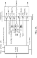
FIG. 1 shows achip 100 with overdrive capability in accordance with an exemplary embodiment of the present invention. Thechip 100 includes acontrol circuit 102 and apost driver 104. Thepost drive 104 has a pull-up circuit 106, a pull-down circuit 108, afirst bias circuit 110, and asecond bias circuit 112. Thecontrol circuit 102 provides a first control signal CS1 and a second control signal CS2 to control the pull-up circuit 106 and the pull-down circuit 108 of thepost driver 104. The details of thepost driver 104 are described in the following paragraphs. - The pull-
up circuit 106 has a plurality of p-channel metal-oxide-semiconductor (PMOS) transistors PI, P2 and P4 coupled in series between an overdrive voltage source (2VDD+VX) and an output terminal OUT of thepost driver 104. The PMOS transistor PI has a drain terminal coupled to the output terminal OUT of thepost driver 104. The pull-down circuit 108 has a plurality of n-channel metal-oxide-semiconductor (NMOS) transistors N1, N2 and N4 coupled in series between the output terminal OUT of thepost driver 104 and a ground terminal VSS(0V). The NMOS transistor N1 has a drain terminal coupled to the output terminal OUT of thepost driver 104. Thefirst bias circuit 110 is configured to provide a first voltage shift (≈VX) between the output terminal OUT of thepost driver 104 and the gate terminal of the PMOS transistor P1 when the pull-down circuit 108 is enabled. The voltage level at the gate terminal of the PMOS transistor P1 is increased by the first voltage shift (≈VX), (e.g., it raises to VX rather than being locked at 0V) when the pull-down circuit 108 is enabled, and the operating voltages supplied on the series of PMOS transistors PI, P2 and P4 in the pull-up circuit 106 are thereby protected within a safe region (within the nominal voltage VDD to avoid the dangerous cross voltage VDD+VX). The PMOS transistors P1, P2 and P4 are all well protected. Thesecond bias circuit 112 is configured to provide a second voltage shift (≈VX) between the output terminal OUT of thepost driver 104 and the gate terminal of the NMOS transistor N1 when the pull-up circuit 106 is enabled. The voltage level at the gate terminal of the NMOS transistor N1 is decreased by the second voltage shift (≈VX), (e.g., it drops to 2VDD rather than being locked at 2VDD+VX) when the pull-up circuit 106 is enabled, and thereby the series of NMOS transistors N1, N2 and N4 in the pull-down circuit 108 are protected within a safe region (within the nominal voltage VDD to avoid the dangerous cross voltage VDD+VX). The NMOS transistors N1, N2 and N4 are all well protected. - In such a design, the overdrive voltage source provides an overdrive voltage that is twice the nominal voltage VDD of the
post driver 104 plus a delta voltage VX, and the first voltage shift and the second voltage shift depend on the delta voltage VX (for example, to balance the delta voltage VX). InFIG. 1 , diode strings are used. Thefirst bias circuit 110 comprises a plurality of diodes coupled in series to provide the first voltage shift (≈VX) when the pull-down circuit 108 is enabled. For example, there may be N diodes (each with a diode voltage VD) in thefirst bias circuit 110, and N∗VD equals the delta voltage VX. Thesecond bias circuit 112 comprises a plurality of diodes coupled in series to provide the second voltage shift (≈VX) when the pull-up circuit 106 is enabled. For example, there may be N diodes (each with a diode voltage VD) in thesecond bias circuit 112, and N∗VD equals the delta voltage VX. - The structure of the
post driver 104 is detailed further below. The PMOS transistor P2 has a drain terminal coupled to the source terminal of the PMOS transistor PI, and a gate terminal biased by the protection voltage PGATE that is the nominal voltage VDD plus the delta voltage VX. The NMOS transistor N2 has a drain terminal coupled to the source terminal of the NMOS transistor N1, and a gate terminal biased by the nominal voltage VDD. Thepost driver 104 also has an NMOS transistor N3 and a PMOS transistor P3. The NMOS transistor N3 has a gate terminal coupled to the drain terminal of the PMOS transistor P2, a drain terminal biased by the protection voltage PGATE (=VDD+VX), and a source terminal coupled to the gate terminal of the PMOS transistor P1. The PMOS transistor P3 has a gate terminal coupled to the drain terminal of the NMOS transistor N2, a drain terminal biased by the nominal voltage VDD, and a source terminal coupled to the gate terminal of the NMOS transistor N1. Referring to the pull-up circuit 106, the PMOS transistor P4 has a source terminal coupled to the overdrive voltage source 2VDD+VX, a drain terminal coupled to a source terminal of the PMOS transistor P2, and a gate terminal receiving the first control signal CS1. Referring to the pull-down circuit 108, the NMOS transistor N4 has a source terminal coupled to the ground terminal VSS (=0V), a drain terminal coupled to a source terminal of the NMOS transistor N2, and a gate terminal receiving the second control signal CS2. - To enable the pull-up
circuit 106 and disable the pull-down circuit 108, thecontrol circuit 102 outputs the protection voltage PGATE (VDD+VX) as the first control signal CS1, and outputs aground voltage 0V as the second control signal CS2. To disable the pull-upcircuit 106 and enable the pull-down circuit 108, thecontrol circuit 102 outputs the overdrive voltage (2VDD+VX) as the first control signal CS1, and outputs the nominal voltage VDD as the second control signal CS2. - Note that the NMOS transistor N3 replaces a conventional multiplexer that was used to change the state of the gate terminal of the PMOS transistor PI, and the PMOS transistor P3 replaces a conventional multiplexer that was used to change the state of the gate terminal of the NMOS transistor N1. Without the conventional multiplexers, the reliability problems due to the multiplexers are removed.
-
FIG. 2A shows a state wherein the pull-upcircuit 106 is enabled, and the pull-down circuit 108 is disabled. In such a situation, thecontrol circuit 102 outputs the protection voltage PGATE (VDD+VX) as the first control signal CS1, and outputs aground voltage 0V as the second control signal CS2. In response to the first control signal CS1 (=PGATE = VDD+VX), the PMOS transistor P4 is turned-on, the drain terminal of the PMOS transistor P4 is at the overdrive voltage 2VDD+VX, the PMOS transistor P2 is tuned on, the drain terminal of the PMOS transistor P2 is at the overdrive voltage 2VDD+VX, ,the NMOS transistor N3 is turned on, the gate terminal of the PMOS transistor P1 is at the protection voltage PGATE (=VDD+VX), the PMOS transistor P1 is turned on, and the output terminal OUT is successfully pulled up to the overdrive voltage 2VDD+VX. The PMOS transistors P1, P2 and P4 and the NMOS transistor N3 are all well protected within the nominal voltage VDD. As for the pull-down circuit 108, in response to the second control signal CS2 (=0V), the NMOS transistors N1, N2 and N4, and the PMOS transistor P3 are all turned off. Note that by thesecond bias circuit 112, the gate terminal of the NMOS transistor N1 is at 2VDD (= (2VDD+VX) - VX), and the source terminal of the NMOS transistor N1 is at 2VDD-Vtn (wherein Vtn is a threshold voltage of an NMOS transistor). The voltage difference between the drain terminal and the gate terminal of the NMOS transistor N2 is (2VDD-Vtn)-VDD, which is VDD-Vtn, and within the nominal voltage VDD. Not only are transistors N1, N4 and P3 protected, but the NMOS transistor N2 is also well protected within the nominal voltage VDD. -
FIG. 2B shows a state wherein the pull-down circuit 108 is enabled, and the pull-upcircuit 106 is disabled. In such a situation, thecontrol circuit 102 outputs the overdrive voltage (2VDD+VX) as the first control signal CS1, and outputs the nominal voltage VDD as the second control signal CS2. In response to the second control signal CS2 (=VDD), the NMOS transistor N4 is turned-on, the drain terminal of the NMOS transistor N4 is at 0V, the NMOS transistor N2 is tuned on, the drain terminal of the NMOS transistor N2 is at 0V, the PMOS transistor P3 is turned on, the gate terminal of the NMOS transistor N1 is at the nominal voltage VDD, the NMOS transistor N1 is turned on, and the output terminal OUT is successfully pulled down to theground voltage 0V. The NMOS transistors N1, N2 and N4 and the PMOS transistor P3 all are well protected within the nominal voltage VDD. As for the pull-upcircuit 106, in response to the first control signal CS1 (=2VDD+VX), the PMOS transistors PI, P2 and P4, and the NMOS transistor N3 are all turned off. Note that by thefirst bias circuit 110, the gate terminal of the PMOS transistor P1 is at VX, and the source terminal of the PMOS transistor P1 is at VX+Vtp (wherein Vtp is a threshold voltage of a PMOS transistor). The voltage difference between the gate terminal and the drain terminal of the PMOS transistor P2 is (VDD+VX)-(VX+Vtp), which is VDD-Vtp, and is within the nominal voltage VDD. The transistors (transistors P1 and P4 and N3, and the PMOS transistor P2) are well protected within the nominal voltage VDD. - In another exemplary embodiment, the first and
second bias circuits second bias circuit 110/112 may be implemented by any device that provides a stable voltage shift. - In another exemplary embodiment, the transistor N3/P3 may be replaced by any switch device.
- In another exemplary embodiment,, the number of PMOS transistors coupled in series between the overdrive voltage source 2VDD+VX and the output terminal OUT is not limited to 3. There may be more PMOS transistors coupled in series in the pull-up
circuit 106. - In another exemplary embodiment,, the number of NMOS transistors coupled in series between output terminal OUT and the ground terminal VSS is not limited to 3. There may be more NMOS transistors coupled in series in the pull-
down circuit 108. - While the invention has been described by way of example and in terms of the preferred embodiments, it should be understood that the invention is not limited to the disclosed embodiments. On the contrary, it is intended to cover various modifications and similar arrangements (as would be apparent to those skilled in the art). Therefore, the scope of the appended claims should be accorded the broadest interpretation so as to encompass all such modifications and similar arrangements.
Claims (15)
- A post driver, comprising:a pull-up circuit, having a plurality of p-channel metal-oxide-semiconductor transistors coupled in series between an overdrive voltage source and an output terminal of the post driver, wherein a first p-channel metal-oxide-semiconductor transistor has a drain terminal coupled to the output terminal of the post driver;a pull-down circuit, having a plurality of n-channel metal-oxide-semiconductor transistors coupled in series between the output terminal of the post driver and a ground terminal, wherein a first n-channel metal-oxide-semiconductor transistor has a drain terminal coupled to the output terminal of the post driver;a first bias circuit, configured to provide a first voltage shift between the output terminal of the post driver and a gate terminal of the first p-channel metal-oxide-semiconductor transistor when the pull-down circuit is enabled, to increase a voltage level at the gate terminal of the first p-channel metal-oxide-semiconductor transistor when the pull-down circuit is enabled; anda second bias circuit, configured to provide a second voltage shift between the output terminal of the post driver and a gate terminal of the first n-channel metal-oxide-semiconductor transistor when the pull-up circuit is enabled, to decrease a voltage level at the gate terminal of the first n-channel metal-oxide-semiconductor transistor when the pull-up circuit is enabled.
- The post driver as claimed in claim 1, wherein:the overdrive voltage source provides an overdrive voltage that is twice a nominal voltage of the post driver plus a delta voltage; andthe first voltage shift and the second voltage shift depend on the delta voltage.
- The post driver as claimed in claim 2, wherein:a second p-channel metal-oxide-semiconductor transistor has a drain terminal coupled to a source terminal of the first p-channel metal-oxide-semiconductor transistor; andwhen the pull-down circuit is enabled, a voltage level at the drain terminal of the second p-channel metal-oxide-semiconductor transistor is raised due to the first voltage shift, and thereby the second p-channel metal-oxide-semiconductor transistor is protected.
- The post driver as claimed in claim 3, wherein:
the gate terminal of the second p-channel metal-oxide-semiconductor transistor is biased by a protection voltage that is the nominal voltage plus the delta voltage. - The post driver as claimed in claim 2, wherein:a second n-channel metal-oxide-semiconductor transistor has a drain terminal coupled to a source terminal of the first n-channel metal-oxide-semiconductor transistor; andwhen the pull-up circuit is enabled, a voltage level at the drain terminal of the second n-channel metal-oxide-semiconductor transistor drops due to the second voltage shift, and thereby the second n-channel metal-oxide-semiconductor transistor is protected.
- The post driver as claimed in claim 5, wherein:
the gate terminal of the second n-channel metal-oxide-semiconductor transistor is biased by the nominal voltage. - The post driver as claimed in claim 4, further comprising:
a third n-channel metal-oxide-semiconductor transistor, having a gate terminal coupled to the drain terminal of the second p-channel metal-oxide-semiconductor transistor, a drain terminal biased by the protection voltage, and a source terminal coupled to the gate terminal of the first p-channel metal-oxide-semiconductor transistor. - The post driver as claimed in claim 7, wherein:
the first bias circuit comprises a plurality of diodes coupled in series to provide the first voltage shift when the pull-down circuit is enabled. - The post driver as claimed in claim 8, wherein:
the first voltage shift balances the delta voltage. - The post driver as claimed in claim 6, further comprising:
a third p-channel metal-oxide-semiconductor transistor, having a gate terminal coupled to the drain terminal of the second n-channel metal-oxide-semiconductor transistor, a drain terminal biased by the nominal voltage, and a source terminal coupled to the gate terminal of the first n-channel metal-oxide-semiconductor transistor. - The post driver as claimed in claim 10, wherein:
the second bias circuit comprises a plurality of diodes coupled in series to provide the second voltage shift when the pull-up circuit is enabled. - The post driver as claimed in claim 11, wherein:
the second voltage shift balances the delta voltage. - The post driver as claimed in claim 7, 8 or 9, wherein:a fourth p-channel metal-oxide-semiconductor transistor has a source terminal coupled to the overdrive voltage source, a drain terminal coupled to a source terminal of the second p-channel metal-oxide-semiconductor transistor, and a gate terminal receiving a first control signal,wherein:to enable the pull-up circuit, the first control signal is at the level of the protection voltage; andto disable the pull-up circuit, the first control signal is twice the nominal voltage plus the delta voltage.
- The post driver as claimed in claim 10, 11 or 12, wherein:a fourth n-channel metal-oxide-semiconductor transistor has a source terminal coupled to the ground terminal, a drain terminal coupled to a source terminal of the second n-channel metal-oxide-semiconductor transistor, and a gate terminal receiving a second control signal,wherein:to enable the pull-down circuit, the second control signal is at the nominal voltage; andto disable the pull-down circuit, the second control signal is at a ground voltage.
- A chip with overdrive capability, comprising:the post driver as claimed in any one of claims 2 to 14; anda control circuit, providing a first control signal and a second control signal to control the pull-up circuit and the pull-down circuit of the post driver.
Applications Claiming Priority (2)
| Application Number | Priority Date | Filing Date | Title |
|---|---|---|---|
| US202163243764P | 2021-09-14 | 2021-09-14 | |
| US17/811,912 US11881847B2 (en) | 2021-09-14 | 2022-07-12 | Post driver and chip with overdrive capability |
Publications (1)
| Publication Number | Publication Date |
|---|---|
| EP4149003A1 true EP4149003A1 (en) | 2023-03-15 |
Family
ID=83232846
Family Applications (1)
| Application Number | Title | Priority Date | Filing Date |
|---|---|---|---|
| EP22194429.1A Pending EP4149003A1 (en) | 2021-09-14 | 2022-09-07 | Post driver and chip with overdrive capability |
Country Status (4)
| Country | Link |
|---|---|
| US (1) | US11881847B2 (en) |
| EP (1) | EP4149003A1 (en) |
| CN (1) | CN115811310A (en) |
| TW (1) | TWI836538B (en) |
Citations (2)
| Publication number | Priority date | Publication date | Assignee | Title |
|---|---|---|---|---|
| US6081152A (en) * | 1998-10-02 | 2000-06-27 | Advanced Micro Devices, Inc. | Output buffer with protective limit of voltage across terminals of devices within the output buffer |
| US10075157B1 (en) * | 2017-04-20 | 2018-09-11 | International Business Machines Corporation | Bidirectional interface using thin oxide devices |
Family Cites Families (11)
| Publication number | Priority date | Publication date | Assignee | Title |
|---|---|---|---|---|
| KR20000041373A (en) * | 1998-12-22 | 2000-07-15 | 김영환 | Output buffer |
| US20030076636A1 (en) | 2001-10-23 | 2003-04-24 | Ming-Dou Ker | On-chip ESD protection circuit with a substrate-triggered SCR device |
| US7737734B1 (en) * | 2003-12-19 | 2010-06-15 | Cypress Semiconductor Corporation | Adaptive output driver |
| US7511534B1 (en) * | 2007-10-05 | 2009-03-31 | Micron Technology, Inc. | Circuits, devices, systems, and methods of operation for a linear output driver |
| US8120968B2 (en) * | 2010-02-12 | 2012-02-21 | International Business Machines Corporation | High voltage word line driver |
| TWI463600B (en) | 2011-03-02 | 2014-12-01 | Global Unichip Corp | 2-stage post driver |
| US8847636B2 (en) * | 2012-04-10 | 2014-09-30 | International Business Machines Corporation | Implementing voltage feedback gate protection for CMOS output drivers |
| KR101989571B1 (en) * | 2012-06-27 | 2019-06-14 | 삼성전자주식회사 | output driver for high voltage and wide range voltage operation and data output driving circuit using the same |
| US8791724B1 (en) | 2013-02-27 | 2014-07-29 | Taiwan Semiconductor Manufacturing Co., Ltd. | Post driver for high density integrated circuits |
| KR20140146368A (en) * | 2013-06-17 | 2014-12-26 | 에스케이하이닉스 주식회사 | Input and output device and system including the same |
| JP6643157B2 (en) * | 2016-03-22 | 2020-02-12 | ルネサスエレクトロニクス株式会社 | Semiconductor device |
-
2022
- 2022-07-12 US US17/811,912 patent/US11881847B2/en active Active
- 2022-07-29 CN CN202210911066.0A patent/CN115811310A/en active Pending
- 2022-08-04 TW TW111129252A patent/TWI836538B/en active
- 2022-09-07 EP EP22194429.1A patent/EP4149003A1/en active Pending
Patent Citations (2)
| Publication number | Priority date | Publication date | Assignee | Title |
|---|---|---|---|---|
| US6081152A (en) * | 1998-10-02 | 2000-06-27 | Advanced Micro Devices, Inc. | Output buffer with protective limit of voltage across terminals of devices within the output buffer |
| US10075157B1 (en) * | 2017-04-20 | 2018-09-11 | International Business Machines Corporation | Bidirectional interface using thin oxide devices |
Also Published As
| Publication number | Publication date |
|---|---|
| US20230081401A1 (en) | 2023-03-16 |
| TWI836538B (en) | 2024-03-21 |
| TW202312677A (en) | 2023-03-16 |
| CN115811310A (en) | 2023-03-17 |
| US11881847B2 (en) | 2024-01-23 |
Similar Documents
| Publication | Publication Date | Title |
|---|---|---|
| US6963226B2 (en) | Low-to-high level shifter | |
| US8947131B2 (en) | Multi-voltage supplied input buffer | |
| US20040140842A1 (en) | Voltage level shift circuit and power supply detection circuit | |
| US7786760B2 (en) | I/O buffer circuit | |
| US11695395B2 (en) | Level shifter | |
| US11916376B2 (en) | Overdrive electrostatic discharge clamp | |
| US11088541B2 (en) | Integrated circuit and electrostatic discharge protection circuit thereof | |
| KR20100016050A (en) | Level shifter circuit incorporating transistor snap-back protection | |
| US11444611B2 (en) | Chip having a receiver including a hysteresis circuit | |
| KR20150000082A (en) | Multi Power supply Type Level Shifter | |
| US8653878B2 (en) | Voltage switch circuit produced by logic circuit manufacturing process capable of withstanding high voltage stress | |
| US10177135B2 (en) | Integrated circuit and electrostatic discharge protection circuit thereof | |
| US6335637B1 (en) | Two-supply protection circuit | |
| CN114825303B (en) | Electrostatic discharge circuit and electrostatic discharge control system | |
| US6201428B1 (en) | 5-volt tolerant 3-volt drive push-pull buffer/driver | |
| US7746145B2 (en) | Level shift circuit capable of preventing occurrence of malfunction when low power supply fluctuates, and semiconductor integrated circuit including the circuit | |
| US9018986B2 (en) | Output buffers | |
| US11632110B2 (en) | High speed circuit with driver circuit | |
| US6628489B1 (en) | Battery and current reversal protect circuit | |
| US11901892B2 (en) | Level shifter and chip with overdrive capability | |
| US11881847B2 (en) | Post driver and chip with overdrive capability | |
| KR20020082232A (en) | Level-shifter for extremely low power supply | |
| US7190191B1 (en) | Over-voltage tolerant input buffer having hot-plug capability | |
| US20230268925A1 (en) | Level shifter | |
| US20090066396A1 (en) | Level shifting circuit |
Legal Events
| Date | Code | Title | Description |
|---|---|---|---|
| PUAI | Public reference made under article 153(3) epc to a published international application that has entered the european phase |
Free format text: ORIGINAL CODE: 0009012 |
|
| STAA | Information on the status of an ep patent application or granted ep patent |
Free format text: STATUS: THE APPLICATION HAS BEEN PUBLISHED |
|
| AK | Designated contracting states |
Kind code of ref document: A1 Designated state(s): AL AT BE BG CH CY CZ DE DK EE ES FI FR GB GR HR HU IE IS IT LI LT LU LV MC MK MT NL NO PL PT RO RS SE SI SK SM TR |
|
| P01 | Opt-out of the competence of the unified patent court (upc) registered |
Effective date: 20230607 |
|
| STAA | Information on the status of an ep patent application or granted ep patent |
Free format text: STATUS: REQUEST FOR EXAMINATION WAS MADE |
|
| 17P | Request for examination filed |
Effective date: 20230915 |
|
| RBV | Designated contracting states (corrected) |
Designated state(s): AL AT BE BG CH CY CZ DE DK EE ES FI FR GB GR HR HU IE IS IT LI LT LU LV MC MK MT NL NO PL PT RO RS SE SI SK SM TR |
|
| STAA | Information on the status of an ep patent application or granted ep patent |
Free format text: STATUS: EXAMINATION IS IN PROGRESS |
|
| 17Q | First examination report despatched |
Effective date: 20241125 |