EP4148954A1 - Electronic device and control method therefor - Google Patents
Electronic device and control method therefor Download PDFInfo
- Publication number
- EP4148954A1 EP4148954A1 EP21818054.5A EP21818054A EP4148954A1 EP 4148954 A1 EP4148954 A1 EP 4148954A1 EP 21818054 A EP21818054 A EP 21818054A EP 4148954 A1 EP4148954 A1 EP 4148954A1
- Authority
- EP
- European Patent Office
- Prior art keywords
- circuit
- modulation
- resonant
- capacitor
- voltage
- Prior art date
- Legal status (The legal status is an assumption and is not a legal conclusion. Google has not performed a legal analysis and makes no representation as to the accuracy of the status listed.)
- Pending
Links
Images











Classifications
-
- H—ELECTRICITY
- H02—GENERATION; CONVERSION OR DISTRIBUTION OF ELECTRIC POWER
- H02J—ELECTRIC POWER NETWORKS; CIRCUIT ARRANGEMENTS OR SYSTEMS FOR SUPPLYING OR DISTRIBUTING ELECTRIC POWER; SYSTEMS FOR STORING ELECTRIC ENERGY
- H02J50/00—Circuit arrangements or systems for wireless supply or distribution of electric power
- H02J50/10—Circuit arrangements or systems for wireless supply or distribution of electric power using inductive coupling
- H02J50/12—Circuit arrangements or systems for wireless supply or distribution of electric power using inductive coupling of the resonant type
-
- H—ELECTRICITY
- H02—GENERATION; CONVERSION OR DISTRIBUTION OF ELECTRIC POWER
- H02J—ELECTRIC POWER NETWORKS; CIRCUIT ARRANGEMENTS OR SYSTEMS FOR SUPPLYING OR DISTRIBUTING ELECTRIC POWER; SYSTEMS FOR STORING ELECTRIC ENERGY
- H02J50/00—Circuit arrangements or systems for wireless supply or distribution of electric power
- H02J50/80—Circuit arrangements or systems for wireless supply or distribution of electric power involving the exchange of data, concerning supply or distribution of electric power, between transmitting devices and receiving devices
-
- H—ELECTRICITY
- H02—GENERATION; CONVERSION OR DISTRIBUTION OF ELECTRIC POWER
- H02J—ELECTRIC POWER NETWORKS; CIRCUIT ARRANGEMENTS OR SYSTEMS FOR SUPPLYING OR DISTRIBUTING ELECTRIC POWER; SYSTEMS FOR STORING ELECTRIC ENERGY
- H02J7/00—Circuit arrangements for charging or discharging batteries or for supplying loads from batteries
- H02J7/02—Circuit arrangements for charging or discharging batteries or for supplying loads from batteries for charging batteries from AC mains by converters
- H02J7/04—Regulation of charging current or voltage
-
- H—ELECTRICITY
- H02—GENERATION; CONVERSION OR DISTRIBUTION OF ELECTRIC POWER
- H02J—ELECTRIC POWER NETWORKS; CIRCUIT ARRANGEMENTS OR SYSTEMS FOR SUPPLYING OR DISTRIBUTING ELECTRIC POWER; SYSTEMS FOR STORING ELECTRIC ENERGY
- H02J7/00—Circuit arrangements for charging or discharging batteries or for supplying loads from batteries
- H02J7/90—Regulation of charging or discharging current or voltage
- H02J7/933—Regulation of charging or discharging current or voltage the cycle being controlled or terminated in response to electric parameters
-
- H—ELECTRICITY
- H02—GENERATION; CONVERSION OR DISTRIBUTION OF ELECTRIC POWER
- H02M—APPARATUS FOR CONVERSION BETWEEN AC AND AC, BETWEEN AC AND DC, OR BETWEEN DC AND DC, AND FOR USE WITH MAINS OR SIMILAR POWER SUPPLY SYSTEMS; CONVERSION OF DC OR AC INPUT POWER INTO SURGE OUTPUT POWER; CONTROL OR REGULATION THEREOF
- H02M3/00—Conversion of DC power input into DC power output
- H02M3/01—Resonant DC/DC converters
-
- H—ELECTRICITY
- H02—GENERATION; CONVERSION OR DISTRIBUTION OF ELECTRIC POWER
- H02M—APPARATUS FOR CONVERSION BETWEEN AC AND AC, BETWEEN AC AND DC, OR BETWEEN DC AND DC, AND FOR USE WITH MAINS OR SIMILAR POWER SUPPLY SYSTEMS; CONVERSION OF DC OR AC INPUT POWER INTO SURGE OUTPUT POWER; CONTROL OR REGULATION THEREOF
- H02M3/00—Conversion of DC power input into DC power output
- H02M3/22—Conversion of DC power input into DC power output with intermediate conversion into AC
- H02M3/24—Conversion of DC power input into DC power output with intermediate conversion into AC by static converters
- H02M3/28—Conversion of DC power input into DC power output with intermediate conversion into AC by static converters using discharge tubes with control electrode or semiconductor devices with control electrode to produce the intermediate AC
- H02M3/325—Conversion of DC power input into DC power output with intermediate conversion into AC by static converters using discharge tubes with control electrode or semiconductor devices with control electrode to produce the intermediate AC using devices of a triode or a transistor type requiring continuous application of a control signal
- H02M3/335—Conversion of DC power input into DC power output with intermediate conversion into AC by static converters using discharge tubes with control electrode or semiconductor devices with control electrode to produce the intermediate AC using devices of a triode or a transistor type requiring continuous application of a control signal using semiconductor devices only
- H02M3/33538—Conversion of DC power input into DC power output with intermediate conversion into AC by static converters using discharge tubes with control electrode or semiconductor devices with control electrode to produce the intermediate AC using devices of a triode or a transistor type requiring continuous application of a control signal using semiconductor devices only of the forward type
- H02M3/33546—Conversion of DC power input into DC power output with intermediate conversion into AC by static converters using discharge tubes with control electrode or semiconductor devices with control electrode to produce the intermediate AC using devices of a triode or a transistor type requiring continuous application of a control signal using semiconductor devices only of the forward type with automatic control of the output voltage or current
- H02M3/33553—Conversion of DC power input into DC power output with intermediate conversion into AC by static converters using discharge tubes with control electrode or semiconductor devices with control electrode to produce the intermediate AC using devices of a triode or a transistor type requiring continuous application of a control signal using semiconductor devices only of the forward type with automatic control of the output voltage or current with galvanic isolation between input and output of both the power stage and the feedback loop
-
- H—ELECTRICITY
- H02—GENERATION; CONVERSION OR DISTRIBUTION OF ELECTRIC POWER
- H02M—APPARATUS FOR CONVERSION BETWEEN AC AND AC, BETWEEN AC AND DC, OR BETWEEN DC AND DC, AND FOR USE WITH MAINS OR SIMILAR POWER SUPPLY SYSTEMS; CONVERSION OF DC OR AC INPUT POWER INTO SURGE OUTPUT POWER; CONTROL OR REGULATION THEREOF
- H02M3/00—Conversion of DC power input into DC power output
- H02M3/22—Conversion of DC power input into DC power output with intermediate conversion into AC
- H02M3/24—Conversion of DC power input into DC power output with intermediate conversion into AC by static converters
- H02M3/28—Conversion of DC power input into DC power output with intermediate conversion into AC by static converters using discharge tubes with control electrode or semiconductor devices with control electrode to produce the intermediate AC
- H02M3/325—Conversion of DC power input into DC power output with intermediate conversion into AC by static converters using discharge tubes with control electrode or semiconductor devices with control electrode to produce the intermediate AC using devices of a triode or a transistor type requiring continuous application of a control signal
- H02M3/335—Conversion of DC power input into DC power output with intermediate conversion into AC by static converters using discharge tubes with control electrode or semiconductor devices with control electrode to produce the intermediate AC using devices of a triode or a transistor type requiring continuous application of a control signal using semiconductor devices only
- H02M3/33569—Conversion of DC power input into DC power output with intermediate conversion into AC by static converters using discharge tubes with control electrode or semiconductor devices with control electrode to produce the intermediate AC using devices of a triode or a transistor type requiring continuous application of a control signal using semiconductor devices only having several active switching elements
- H02M3/33576—Conversion of DC power input into DC power output with intermediate conversion into AC by static converters using discharge tubes with control electrode or semiconductor devices with control electrode to produce the intermediate AC using devices of a triode or a transistor type requiring continuous application of a control signal using semiconductor devices only having several active switching elements having at least one active switching element at the secondary side of an isolation transformer
-
- H—ELECTRICITY
- H02—GENERATION; CONVERSION OR DISTRIBUTION OF ELECTRIC POWER
- H02M—APPARATUS FOR CONVERSION BETWEEN AC AND AC, BETWEEN AC AND DC, OR BETWEEN DC AND DC, AND FOR USE WITH MAINS OR SIMILAR POWER SUPPLY SYSTEMS; CONVERSION OF DC OR AC INPUT POWER INTO SURGE OUTPUT POWER; CONTROL OR REGULATION THEREOF
- H02M3/00—Conversion of DC power input into DC power output
- H02M3/22—Conversion of DC power input into DC power output with intermediate conversion into AC
- H02M3/24—Conversion of DC power input into DC power output with intermediate conversion into AC by static converters
- H02M3/28—Conversion of DC power input into DC power output with intermediate conversion into AC by static converters using discharge tubes with control electrode or semiconductor devices with control electrode to produce the intermediate AC
- H02M3/325—Conversion of DC power input into DC power output with intermediate conversion into AC by static converters using discharge tubes with control electrode or semiconductor devices with control electrode to produce the intermediate AC using devices of a triode or a transistor type requiring continuous application of a control signal
- H02M3/335—Conversion of DC power input into DC power output with intermediate conversion into AC by static converters using discharge tubes with control electrode or semiconductor devices with control electrode to produce the intermediate AC using devices of a triode or a transistor type requiring continuous application of a control signal using semiconductor devices only
- H02M3/33569—Conversion of DC power input into DC power output with intermediate conversion into AC by static converters using discharge tubes with control electrode or semiconductor devices with control electrode to produce the intermediate AC using devices of a triode or a transistor type requiring continuous application of a control signal using semiconductor devices only having several active switching elements
- H02M3/33576—Conversion of DC power input into DC power output with intermediate conversion into AC by static converters using discharge tubes with control electrode or semiconductor devices with control electrode to produce the intermediate AC using devices of a triode or a transistor type requiring continuous application of a control signal using semiconductor devices only having several active switching elements having at least one active switching element at the secondary side of an isolation transformer
- H02M3/33584—Bidirectional converters
-
- H—ELECTRICITY
- H03—ELECTRONIC CIRCUITRY
- H03H—IMPEDANCE NETWORKS, e.g. RESONANT CIRCUITS; RESONATORS
- H03H11/00—Networks using active elements
- H03H11/02—Multiple-port networks
- H03H11/28—Impedance matching networks
-
- H—ELECTRICITY
- H04—ELECTRIC COMMUNICATION TECHNIQUE
- H04B—TRANSMISSION
- H04B5/00—Near-field transmission systems, e.g. inductive or capacitive transmission systems
- H04B5/40—Near-field transmission systems, e.g. inductive or capacitive transmission systems characterised by components specially adapted for near-field transmission
- H04B5/48—Transceivers
-
- H—ELECTRICITY
- H04—ELECTRIC COMMUNICATION TECHNIQUE
- H04B—TRANSMISSION
- H04B5/00—Near-field transmission systems, e.g. inductive or capacitive transmission systems
- H04B5/70—Near-field transmission systems, e.g. inductive or capacitive transmission systems specially adapted for specific purposes
- H04B5/79—Near-field transmission systems, e.g. inductive or capacitive transmission systems specially adapted for specific purposes for data transfer in combination with power transfer
-
- H—ELECTRICITY
- H02—GENERATION; CONVERSION OR DISTRIBUTION OF ELECTRIC POWER
- H02J—ELECTRIC POWER NETWORKS; CIRCUIT ARRANGEMENTS OR SYSTEMS FOR SUPPLYING OR DISTRIBUTING ELECTRIC POWER; SYSTEMS FOR STORING ELECTRIC ENERGY
- H02J2207/00—Details of circuit arrangements for charging or discharging batteries or supplying loads from batteries
- H02J2207/20—Charging or discharging characterised by the power electronics converter
-
- H—ELECTRICITY
- H02—GENERATION; CONVERSION OR DISTRIBUTION OF ELECTRIC POWER
- H02M—APPARATUS FOR CONVERSION BETWEEN AC AND AC, BETWEEN AC AND DC, OR BETWEEN DC AND DC, AND FOR USE WITH MAINS OR SIMILAR POWER SUPPLY SYSTEMS; CONVERSION OF DC OR AC INPUT POWER INTO SURGE OUTPUT POWER; CONTROL OR REGULATION THEREOF
- H02M3/00—Conversion of DC power input into DC power output
- H02M3/01—Resonant DC/DC converters
- H02M3/015—Resonant DC/DC converters with means for adaptation of resonance frequency, e.g. by modification of capacitance or inductance of resonance circuit
-
- Y—GENERAL TAGGING OF NEW TECHNOLOGICAL DEVELOPMENTS; GENERAL TAGGING OF CROSS-SECTIONAL TECHNOLOGIES SPANNING OVER SEVERAL SECTIONS OF THE IPC; TECHNICAL SUBJECTS COVERED BY FORMER USPC CROSS-REFERENCE ART COLLECTIONS [XRACs] AND DIGESTS
- Y02—TECHNOLOGIES OR APPLICATIONS FOR MITIGATION OR ADAPTATION AGAINST CLIMATE CHANGE
- Y02B—CLIMATE CHANGE MITIGATION TECHNOLOGIES RELATED TO BUILDINGS, e.g. HOUSING, HOUSE APPLIANCES OR RELATED END-USER APPLICATIONS
- Y02B70/00—Technologies for an efficient end-user side electric power management and consumption
- Y02B70/10—Technologies improving the efficiency by using switched-mode power supplies [SMPS], i.e. efficient power electronics conversion e.g. power factor correction or reduction of losses in power supplies or efficient standby modes
Definitions
- This application relates to the field of wireless charging technologies, and in particular, to an electronic device and a control method for the electronic device.
- a wireless charging technology is to induce energy from a primary coil of a power transmitting terminal device to a secondary coil of a power receiving terminal device through near-field electromagnetic induction, thereby completing power transmission.
- a power receiving terminal device in wireless charging needs to be adapted to power transmitting terminal devices that satisfy a Qi standard, including a mobile phone, a tablet, a charging chassis, and the like supporting a reverse charging function.
- Transmitting terminals of different brands use different rectifier circuit (for example, alternating current (alternating current, AC) to direct current (direct current, DC) conversion, AC/DC) topologies, modulation modes, circuit parameters, operating frequencies, and control logic. Therefore, for different power transmitting terminal devices, the power receiving terminal device may not satisfy specifications of the Qi standard.
- ASK modulation is to modulate transmit power signal load through reverse reflection to achieve an objective of information transmission. As the load in the ASK modulation changes, a power signal envelope alternately appears to be in a high (high) or low (low) state.
- Embodiments of this application provide an electronic device and a control method for the electronic device, to improve compatibility of a power receiving terminal device in wireless charging with a power transmitting terminal device by improving ASK communication quality.
- an electronic device includes a device circuit, a voltage conversion circuit, a rectifier circuit, a resonant circuit, and a modulation circuit.
- An input end of the device circuit is coupled to an output end of the voltage conversion circuit, an input end of the voltage conversion circuit is coupled to an output end of the rectifier circuit, an input end of the rectifier circuit is coupled to an output end of the resonant circuit, and the modulation circuit is coupled to the input end of the rectifier circuit.
- the resonant circuit is configured to induce an alternating magnetic field sent by a power transmitting terminal device to generate an induced alternating current; the modulation circuit is configured to modulate an amplitude of the induced alternating current; the rectifier circuit is configured to rectify the amplitude-modulated induced alternating current to generate a rectified voltage; and the voltage conversion circuit is configured to convert the rectified voltage into a load voltage and output the load voltage to the device circuit.
- the resonant circuit includes a resonant inductor and a resonant capacitor control circuit connected in series to the resonant inductor.
- a first end of the resonant inductor is coupled to the rectifier circuit, a second end of the resonant inductor is coupled to a first end of the resonant capacitor control circuit, and a second end of the resonant capacitor control circuit is coupled to the rectifier circuit.
- the resonant capacitor control circuit is configured to adjust a capacitance value of a resonant capacitor connected to the resonant circuit.
- the resonant capacitor control circuit can adjust the capacitance value of the resonant capacitor connected to the resonant circuit.
- a gain of the rectified voltage can be indirectly adjusted by adjusting the resonant capacitor, so that a problem of negative ASK modulation or decrease or increase of a voltage difference of the rectified voltage is resolved. Therefore, ASK communication quality is improved, and compatibility of the electronic device in wireless charging is improved.
- the resonant capacitor control circuit includes a capacitance value switching network formed by at least one switch and at least one capacitor, and the resonant capacitor control circuit is configured to control a status of the switch to adjust the capacitance value of the resonant capacitor connected to the resonant circuit.
- the resonant capacitor control circuit includes an adjustable capacitor, a first end of the adjustable capacitor is coupled to the second end of the resonant inductor, and a second end of the adjustable capacitor is coupled to the rectifier circuit.
- the resonant capacitor control circuit includes at least two parallel resonant capacitor regulating branches.
- a first end of the resonant capacitor regulating branch is coupled to the second end of the resonant inductor, and a second end of the resonant capacitor regulating branch is coupled to the rectifier circuit.
- a first switch and a first capacitor are connected in series on at least one resonant capacitor regulating branch, and the resonant capacitor control circuit adjusts, by adjusting a status of a first switch on the at least one resonant capacitor regulating branch, the capacitance value of the resonant capacitor connected to the resonant circuit.
- One resonant capacitor regulating branch includes a second capacitor, a first end of the second capacitor is coupled to the second end of the resonant inductor, and a second end of the second capacitor is coupled to the rectifier circuit.
- the first switch includes a bidirectional switching transistor.
- the device circuit is further configured to detect the rectified voltage.
- the resonant capacitor control circuit increases the capacitance value of the resonant capacitor connected to the resonant circuit, to recover positive modulation of the rectified voltage.
- the resonant capacitor is connected in series in the resonant circuit, during power transmission, main power is transmitted by using the resonant capacitor. Therefore, adjusting the resonant capacitor causes system instability. Therefore, capacitive reactance of ASK modulation is usually not optimized by adjusting the resonant capacitor.
- the resonant capacitor is mainly adjusted during negative ASK modulation.
- the electronic device further includes a load control circuit.
- the load control circuit is coupled to the input end of the rectifier circuit, and the load control circuit is configured to connect a resistance value to the input end of the rectifier circuit when the rectified voltage is at a low level.
- the load control circuit can connect the resistance value to the input end of the rectifier circuit when the rectified voltage is at the low level, and a modulation capacitor is disconnected when the rectified voltage is at the low level. In this case, a voltage gain needs to be reduced. Because the resistance value is connected to the input end of the rectifier circuit, energy of the input end of the rectifier circuit can be forcibly released when the modulation capacitor is disconnected. In this way, continuous increase of a voltage of a capacitor is avoided, and a modulation waveform is improved by dividing the rectified voltage. For example, low level burrs or oscillations are eliminated.
- the device circuit is further configured to detect power corresponding to the rectified voltage and power consumed by the resistance value connected by the load control circuit to the input end of the rectifier circuit; and the load control circuit is configured to disconnect the resistance value when it is determined that the power corresponding to the rectified voltage is greater than the power consumed by the resistance value.
- the electronic device further includes: the modulation circuit is configured to adjust a capacitance value of a modulation capacitor connected to the input end of the rectifier circuit.
- the modulation circuit can adjust the capacitance value of the modulation capacitor connected to the input end of the rectifier circuit, and the gain of the rectified voltage can be indirectly adjusted by adjusting the value of the modulation capacitor, so that the problem of negative ASK modulation or decrease or increase of the voltage difference of the rectified voltage Vrect is resolved. Therefore, ASK communication quality is improved, and compatibility of the electronic device in wireless charging is improved.
- the device circuit is further configured to detect the rectified voltage; and when a maximum voltage difference of the rectified voltage is less than or equal to a first threshold voltage and the rectified voltage is at the low level, the modulation circuit is configured to increase the capacitance value of the modulation capacitor connected to the input end of the rectifier circuit; or when a maximum voltage difference of the rectified voltage is greater than or equal to a second threshold voltage and the rectified voltage is at the low level, the modulation circuit is configured to reduce the capacitance value of the modulation capacitor connected to the input end of the rectifier circuit, where the second threshold voltage is greater than the first threshold voltage.
- the resonant capacitor is connected in series in the resonant circuit, during power transmission, main power is transmitted by using the resonant capacitor. Therefore, adjusting the resonant capacitor causes system instability. Therefore, capacitive reactance of ASK modulation is usually not optimized by adjusting the resonant capacitor. However, when negative ASK modulation occurs, ASK communication fails directly. Therefore, in this application, the resonant capacitor is mainly adjusted during negative ASK modulation. A main cause of negative ASK modulation is that the resonant capacitor is overcompensated.
- an electronic device includes a device circuit, a voltage conversion circuit, a rectifier circuit, a resonant circuit, and a modulation circuit.
- An input end of the device circuit is coupled to an output end of the voltage conversion circuit, an input end of the voltage conversion circuit is coupled to an output end of the rectifier circuit, an input end of the rectifier circuit is coupled to an output end of the resonant circuit, and the modulation circuit is coupled to the input end of the rectifier circuit.
- the resonant circuit is configured to induce an alternating magnetic field sent by a power transmitting terminal device to generate an induced alternating current; the modulation circuit is configured to modulate an amplitude of the alternating current; the rectifier circuit is configured to rectify the amplitude-modulated induced alternating current to generate a rectified voltage; and the voltage conversion circuit is configured to convert the rectified voltage into a load voltage and output the load voltage to the device circuit.
- the electronic device further includes a load control circuit.
- the load control circuit is coupled to the input end of the rectifier circuit, and the load control circuit is configured to connect a resistance value to the input end of the rectifier circuit when the rectified voltage is at a low level.
- the load control circuit can connect the resistance value to the input end of the rectifier circuit when the rectified voltage is at the low level, and a modulation capacitor is disconnected when the rectified voltage is at the low level. In this case, a voltage gain needs to be reduced. Because the resistance value is connected to the input end of the rectifier circuit, energy of the input end of the rectifier circuit can be forcibly released when the modulation capacitor is disconnected. In this way, continuous increase of a voltage of a capacitor is avoided, and a modulation waveform is improved by dividing the rectified voltage. For example, low level burrs or oscillations are eliminated.
- the load control circuit includes a resistance value switching network formed by at least one switch and at least one resistor, and the load control circuit is configured to control a status of the switch to adjust the resistance value connected to the input end of the rectifier circuit.
- the load control circuit includes a first switch and a first resistor, a first end of the first resistor is coupled to the input end of the rectifier circuit, a second end of the first resistor is coupled to a first end of the first switch, and a second end of the first switch is grounded.
- the device circuit is further configured to detect power corresponding to the rectified voltage and power consumed by the resistance value connected by the load control circuit to the input end of the rectifier circuit; and the load control circuit is configured to disconnect the resistance value when it is determined that the power corresponding to the rectified voltage is greater than the power consumed by the resistance value.
- an electronic device includes a device circuit, a voltage conversion circuit, a rectifier circuit, a resonant circuit, and a modulation circuit.
- An input end of the device circuit is coupled to an output end of the voltage conversion circuit, an input end of the voltage conversion circuit is coupled to an output end of the rectifier circuit, an input end of the rectifier circuit is coupled to an output end of the resonant circuit, and the modulation circuit is coupled to the input end of the rectifier circuit.
- the resonant circuit is configured to induce an alternating magnetic field sent by a power transmitting terminal device to generate an induced alternating current;
- the modulation circuit is configured to modulate an amplitude of the alternating current;
- the rectifier circuit is configured to rectify the amplitude-modulated induced alternating current to generate a rectified voltage;
- the voltage conversion circuit is configured to convert the rectified voltage into a load voltage and output the load voltage to the device circuit; and the modulation circuit is configured to adjust a capacitance value of a modulation capacitor connected to the input end of the rectifier circuit.
- the modulation circuit can adjust the capacitance value of the modulation capacitor connected to the input end of the rectifier circuit, and a gain of the rectified voltage can be indirectly adjusted by adjusting the value of the modulation capacitor, so that a problem of negative ASK modulation or decrease or increase of a voltage difference of the rectified voltage Vrect is resolved. Therefore, ASK communication quality is improved, and compatibility of the electronic device in wireless charging is improved.
- the modulation circuit includes a capacitance value switching network formed by at least one switch and at least one capacitor, and the modulation circuit is configured to control a status of the switch to adjust the capacitance value of the modulation capacitor connected to the input end of the rectifier circuit.
- the modulation circuit includes a first switch and an adjustable capacitor, a first end of the adjustable capacitor is coupled to the input end of the rectifier circuit, a second end of the adjustable capacitor is coupled to a first end of the first switch, and a second end of the first switch is coupled to the ground.
- the modulation circuit includes a first switch and at least two parallel modulation capacitor branches, a first end of the modulation capacitor branch is coupled to the input end of the rectifier circuit, a second end of the modulation capacitor branch is coupled to a first end of the first switch, and a second end of the first switch is coupled to the ground.
- the modulation capacitor branch includes a first capacitor and a second switch, a first end of the second switch is coupled to the input end of the rectifier circuit, a second end of the second switch is coupled to a first end of the first capacitor, and a second end of the first capacitor is coupled to the first end of the first switch.
- the modulation circuit adjusts, by adjusting a status of the second switch on the at least one modulation capacitor branch, the capacitance value of the modulation capacitor connected to the input end of the rectifier circuit.
- a second capacitor is connected in series on one modulation capacitor branch.
- the device circuit is further configured to detect the rectified voltage; and when a maximum voltage difference of the rectified voltage is less than or equal to a first threshold voltage and the rectified voltage is at a low level, the modulation circuit is configured to increase the capacitance value of the modulation capacitor connected to the input end of the rectifier circuit; or when a maximum voltage difference of the rectified voltage is greater than or equal to a second threshold voltage and the rectified voltage is at a low level, the modulation circuit is configured to reduce the capacitance value of the modulation capacitor connected to the input end of the rectifier circuit, where the second threshold voltage is greater than the first threshold voltage.
- the resonant capacitor is connected in series in the resonant circuit, during power transmission, main power is transmitted by using the resonant capacitor. Therefore, adjusting the resonant capacitor causes system instability. Therefore, capacitive reactance of ASK modulation is usually not optimized by adjusting the resonant capacitor. However, when negative ASK modulation occurs, ASK communication fails directly. Therefore, in this application, the resonant capacitor is mainly adjusted during negative ASK modulation. A main cause of negative ASK modulation is that the resonant capacitor is overcompensated.
- a control method for the electronic device provided in the first aspect includes a resonant inductor and a resonant capacitor control circuit connected in series to the resonant inductor.
- the control method for the electronic device includes: a device circuit detects a rectified voltage, and when negative modulation of the rectified voltage occurs, the resonant capacitor control circuit adjusts a capacitance value of a resonant capacitor connected to the resonant circuit, to recover positive modulation of the rectified voltage.
- that the resonant capacitor control circuit adjusts a capacitance value of a resonant capacitor connected to the resonant circuit includes: the resonant capacitor control circuit increases the capacitance value of the resonant capacitor connected to the resonant circuit.
- the electronic device further includes a load control circuit; and when the rectified voltage is modulated by positive modulation, the control method includes: the load control circuit connects a resistance value to an input end of the rectifier circuit when the rectified voltage is at a low level.
- control method further includes: power corresponding to the rectified voltage and power consumed by the resistance value connected by the load control circuit to the input end of the rectifier circuit are detected; and the load control circuit disconnects the resistance value when it is determined that the power corresponding to the rectified voltage is greater than the power consumed by the resistance value.
- the control method when the rectified voltage is modulated by positive modulation, the control method further includes: when a maximum voltage difference of the rectified voltage is less than or equal to a first threshold voltage and the rectified voltage is at the low level, a modulation circuit increases a capacitance value of a modulation capacitor connected to the input end of the rectifier circuit; or when a maximum voltage difference of the rectified voltage is greater than or equal to a second threshold voltage and the rectified voltage is at the low level, a modulation circuit reduces a capacitance value of a modulation capacitor connected to the input end of the rectifier circuit, where the second threshold voltage is greater than the first threshold voltage.
- first and second mentioned below are merely intended for a purpose of description, and shall not be understood as an indication or implication of relative importance or implicit indication of a quantity of indicated technical features. Therefore, a feature limited by “first” or “second” may explicitly indicate or implicitly include one or more such features. In the description of embodiments of this application, unless otherwise stated, "a plurality of" means two or more.
- directional terms such as “up”, “down”, “left”, and “right” may include but are not limited to those defined relative to directions in which components are placed in the accompanying drawings. It should be understood that the directional terms may be relative concepts. The directional terms are used for relative description and clarification, and may vary accordingly depending on changes of the directions in which the components are placed in the accompanying drawings.
- connection should be understood in a broad sense.
- connection may refer to a fixed connection, a detachable connection, or an integral connection, and may refer to a direct connection or an indirect connection via an intermediate medium.
- coupling may be an electrical connection for implementing signal transmission.
- the “coupling” may be a direct electrical connection or an indirect electrical connection via an intermediate medium.
- Embodiments of this application are applied to a wireless charging system and used to implement WPC (wireless power consortium, WPC) wireless charging.
- a WPC wireless charging technology is to induce energy from a primary coil n1 to a secondary coil n2 through near-field electromagnetic induction (for example, magnetic lines shown in FIG. 1 ), thereby completing power transmission.
- Two power profiles for low and medium power devices include: a baseline power profile (baseline power profile, BPP, BPP ⁇ 5 W); and extended power profile (extended power profile, EPP, EPP ⁇ 15 W).
- the WPC wireless charging system includes a power transmitting terminal device and a power receiving terminal device.
- the wireless charging system 10 includes two electronic devices, and one electronic device can wirelessly charge the other electronic device. As shown in FIG.
- the first electronic device 01 includes a mobile phone (mobile phone), a tablet computer (pad), a computer with a wireless transceiver function, an intelligent wearable product (for example, a smart watch or a smart band), a virtual reality (virtual reality, VR) terminal device, an augmented reality (augmented reality, AR) terminal device, or the like that has a wireless device.
- the first electronic device 01 may be an electronic product such as a wireless charging electric vehicle, a wireless charging household small electric appliance (such as a soymilk maker or a vacuum cleaning robot), or an unmanned aerial vehicle.
- a specific form of the first electronic device 01 is not specifically limited in embodiments of this application. For ease of description, it is hereinafter assumed that the first electronic device 01 is the mobile phone shown in FIG. 1 .
- the first electronic device 01 mainly includes a display screen (display panel, DP) 101.
- the display screen 101 may be a liquid crystal display (liquid crystal display, LCD) screen or an organic light emitting diode (organic light emitting diode, OLED) display screen. This is not limited in embodiments of this application.
- the electronic device 01 further includes a middle frame 111 and a housing 112 shown in FIG. 2 .
- the display screen 100 and the housing 112 are respectively located on two sides of the middle frame 111, a rear face of the display screen 100 faces the housing 112, and the display screen 100 and the housing 112 may be connected by the middle frame 111.
- the wireless charging receiving circuit 20 may be disposed on one side of the middle frame 111 facing the housing 112.
- the device circuit 50 may include components such as a processor, a radio frequency (radio frequency, RF) circuit, a power supply, a memory, an input unit, a display unit, and an audio circuit.
- RF radio frequency
- the device circuit 50 is merely an example herein, and may further include more or fewer components than the foregoing.
- the second electronic device 02 includes a wireless charging circuit 30 disposed in the charger 02 and a power supply 40 coupled to the wireless charging circuit 30, as shown in FIG. 1 .
- the power supply 40 is configured to provide charging electric energy.
- the power supply 40 may be a power adapter.
- the power supply 40 may convert a 220 V alternating current into a direct current (for example, 5 V or 10 V) based on a charging power requirement, and transmit the direct current to the wireless charging circuit 30.
- the second electronic device 02 may alternatively be a mobile phone, a tablet computer, or the like, to implement mutual charging between electronic devices.
- the wireless charging system 10 can implement power transmission and communication transmission between the two electronic devices.
- a power transmission process includes: the second electronic device 02 converts input electric energy into electromagnetic energy by using a voltage converter; and the first electronic device 01 converts electromagnetic energy in a magnetic field into electric energy by using a rectifier circuit and outputs the electric energy to the subsequent device circuit for use.
- a communication transmission process includes: the second electronic device 02 supports ASK modulation or FSK modulation, and the first electronic device 01 supports ASK modulation or FSK demodulation; therefore, a power transmitting terminal device modulates a communication transmission signal onto electromagnetic energy for power transmission, and a power receiving terminal device demodulates the communication transmission signal from the electromagnetic energy.
- ASK modulation is a mandatory functional part.
- Embodiments of this application mainly relate to ASK modulation. Therefore, the following example mainly uses ASK modulation as an example for description.
- the wireless charging circuit 30 includes a voltage converter 301 and a TX (transport, transmit) resonant circuit 302.
- the voltage converter 301 may be a DC to AC converter, that is, DC/AC.
- a specific circuit of the TX resonant circuit 302 is provided.
- the circuit includes a TX resonant capacitor C1 and a TX resonant inductor L1 (that is, the primary coil n1 in FIG. 1 ), where C1 and L1 are connected in series to an output end of the voltage converter 301.
- the wireless charging receiving circuit 20 further includes an RX (receive, receive) resonant circuit 201 and a rectifier circuit 202.
- the voltage converter 301 is coupled to the power supply 40, and can convert a direct current output by the power supply 40 into an alternating current.
- the TX resonant circuit 302 is coupled to the voltage converter 301. After receiving the alternating current output by the voltage converter 301, the TX resonant circuit 302 may generate an alternating magnetic field.
- the RX resonant circuit 201 receives the alternating magnetic field and outputs an induced alternating current, so that power of the TX resonant circuit 302 can be transmitted to the RX resonant circuit 201. As shown in FIG.
- the circuit includes an RX resonant capacitor C2 and an RX resonant inductor L2 (that is, the secondary coil n2 in FIG. 1 ) that are connected in series.
- the RX resonant circuit 201 is coupled to the rectifier circuit 202, and the rectifier circuit 202 may rectify the induced alternating current output by the RX resonant circuit 201, to generate a rectified voltage Vrect.
- the rectifier circuit 202 may be an alternating current to direct current converter, that is, AC/DC. An example drawing of the rectifier circuit 202 is shown in FIG. 4 .
- the rectifier circuit 202 includes four switching transistors Q1 to Q4, where Q1 and Q4 are connected to form a full-bridge rectifier.
- the TX resonant circuit 302 is connected to two input ends AC1 and AC2 of the full-bridge rectifier, the induced alternating current is input to the full-bridge rectifier through AC1 and AC2, and the full-bridge rectifier rectifies the induced alternating current and outputs the rectified voltage Vrect at an output end.
- a rectifier capacitor C3 and a resistor R1 are connected in parallel at the output end of the full-bridge rectifier, where the resistor R1 provides an energy discharge channel for C3.
- the wireless charging receiving apparatus 20 further includes at least one voltage conversion circuit 203 coupled to the rectifier circuit 202.
- the voltage conversion circuit 203 may convert the rectified voltage Vrect into a load voltage, and output the load voltage to the device circuit 50 to supply power to the device circuit 50.
- the voltage conversion circuit 203 converts the rectified voltage Vrect into a charging voltage (for example, 3.7 V). After the charging voltage is applied to both ends of the battery, a current output by the voltage conversion circuit 203 can charge the battery 50.
- the voltage conversion circuit 203 includes a DC/DC conversion circuit.
- the DC/DC conversion circuit may be a buck (Buck) circuit, a switched capacitor (switched capacitor, SC) circuit, or a low dropout linear regulator (low dropout regulator, LDO).
- An input/output voltage ratio of the buck circuit may be flexibly adjusted. For example, the input/output voltage ratio may be set to a decimal.
- An input/output voltage ratio of the SC circuit is an integer, but the SC circuit can withstand a relatively high difference between an input voltage and an output voltage and has relatively high voltage conversion efficiency. An input voltage is relatively close to an output voltage of the LDO, and voltage conversion efficiency is relatively high. As shown in FIG.
- a filter capacitor C4 is further connected in parallel at an output end of the LDO.
- a detection capacitor Cdet is further connected in parallel at an output end of the RX resonant circuit 201. Because the detection capacitor Cdet is disposed in the first electronic device 10, in the wireless charging system, when the first electronic device 10 is placed near the second electronic device 20, the detection capacitor Cdet can change a resonant frequency of the wireless charging system. After sampling the resonant frequency, the second electronic device 20 determines that the first electronic device 10 is waiting to be charged.
- the wireless charging receiving circuit 20 further includes an ASK modulation circuit 204
- the wireless receiving circuit 30 further includes an ASK demodulation circuit 303.
- ASK modulation is to modulate transmit power signal load through reverse reflection to achieve an objective of information transmission.
- the ASK modulation circuit 204 modulates a received transmit power signal into a waveform signal by adjusting the transmit power signal load (for example, impedance or capacitive reactance) in the power receiving terminal device, so that a communication transmission signal is carried in the waveform signal.
- the ASK demodulation circuit 303 demodulates the communication transmission signal based on the reversely reflected waveform signal received by the power transmitting terminal device. Specifically, an example is as follows: The Qi protocol specifies that an internal clock in ASK modulation is 2 kHz, and a differential biphase coding scheme is used to modulate data bits onto power signals transmitted by the power receiving terminal device and the power transmitting terminal device. As shown in FIG.
- the differential biphase coding scheme is described as follows: In one clock cycle (or modulation cycle), a modulation waveform of a voltage or a current changes twice, the power receiving terminal device encodes (encode) 1 for outputting, and the power transmitting terminal device decodes (decode) 1; the waveform of the voltage or current changes once, the power receiving terminal device encodes 0 for outputting, and the power transmitting terminal device decodes (decode) 0. If a positive maximum amplitude (and a negative maximum amplitude) of the modulation waveform remains unchanged in one clock cycle, it is considered that the voltage or current changes once.
- the power receiving terminal device uses two ASK modulation modes: a capacitive mode and a resistive mode. As shown in FIG. 4 and FIG. 6 , capacitive ASK modulation changes a load characteristic of the power receiving terminal device by coupling two capacitors Cm1 and Cm2 to two input ends AC1 and AC2 of the rectifier circuit 202, thereby changing a voltage gain of the entire circuit and ultimately changing an amplitude of a power signal.
- the capacitor Cm1 and a switch Q5 are connected in series between the input end AC1 of the rectifier circuit and the ground GND, and the capacitor Cm2 and a switch Q6 are connected in series between the input end AC2 of the rectifier circuit and the ground GND, where turn-on/off of the switches Q5 and Q6 is controlled by an ASK modulation drive circuit.
- the switches Q5 and Q6 are in different states, the load in the ASK modulation changes, and a power signal envelope alternately appears to be in a high (HI) or low (LO) state.
- the modulation waveform needs to be modulated to a relatively high amplitude (High level, which is used as an example in all the following schemes), Q5 may be controlled to be turned on, and Cm1 may be controlled to be connected to AC1; or when the modulation waveform needs to be modulated to a relatively low amplitude (Low level, which is used as an example in all the following schemes), Q5 may be controlled to be turned off, and Cm1 may be controlled to be disconnected from AC1.
- High level which is used as an example in all the following schemes
- Q5 may be controlled to be turned on
- Cm1 may be controlled to be connected to AC1
- Low level which is used as an example in all the following schemes
- Q6 when the modulation waveform needs to be modulated to a relatively high amplitude (high level), Q6 may be controlled to be turned on, and Cm2 may be controlled to be connected to AC2; or when the modulation waveform needs to be modulated to a relatively low amplitude (low level), Q6 may be controlled to be turned off, and Cm2 may be controlled to be disconnected from AC2.
- positive modulation also referred to as positive ASK modulation in the following schemes
- Q5 and Q6 may be switching transistors, and a gate of the switching transistor is coupled to the ASK modulation drive circuit to receive a gating signal of the ASK modulation drive circuit and control turn-on/off of Q5 and Q6.
- modulation capacitors are connected to AC 1 and AC2 if the modulation waveform is modulated to a relatively low amplitude, but the modulation waveform is modulated to a relatively high amplitude after the modulation capacitors are disconnected from AC1 and AC2, the modulation is negative modulation (also referred to as negative ASK modulation in the following schemes). As shown in FIG.
- resistive ASK modulation changes the load characteristic of the receiving terminal by connecting two parallel resistors Rm1 and Rm2 to an output end of the rectifier, thereby changing the voltage gain of the entire circuit and ultimately changing the amplitude of the transmit power signal.
- the resistor Rm1 and a switch Q7 are connected in series between the output end Vrect of the rectifier circuit and the ground GND
- the resistor Rm2 and a switch Q8 are connected in series between the output end Vrect of the rectifier circuit and the ground GND, where turn-on/off of the switches Q7 and Q8 is controlled by the ASK modulation drive circuit, and Q7 and Q8 may be switching transistors.
- the wireless charging receiving circuit 20 further includes an RX control system 205
- the wireless charging circuit 30 further includes a TX control system 304.
- the RX control system 205 and the TX control system 304 may transmit a control signal by using the communication transmission established between the first electronic device 10 and the second electronic device 20, to control the power transmission and the communication transmission process.
- the control signal may be transmitted or charging data may be transmitted.
- the charging data may be used to indicate a charging type, charging power, or the like.
- the power receiving terminal device in wireless charging needs to be adapted to all power transmitting terminal devices that satisfy the Qi standard, including a mobile phone, a tablet, a charging chassis, and the like supporting a reverse charging function.
- Transmitting terminal devices of different brands use different AC_DC converter topologies, modulation modes, circuit parameters, operating frequencies, and control logic. Therefore, for different power transmitting terminal devices, the power receiving terminal device cannot satisfy specifications of the Qi protocol.
- the load in ASK modulation changes, the power signal envelope alternately appears to be in the high (HI) or low (LO) state.
- a change of a high/low state current is greater than 15 mA or a change of a high/low voltage is greater than 200 mV
- information transmitted by a power signal envelope is valid
- a change of a high/low state current is less than 8 mA or a change of a voltage is less than 100 mV
- information transmitted by a power signal envelope is invalid.
- the power signal needs to ensure a valid voltage difference or current difference.
- a wireless charging compatibility test item is a difficulty in obtaining wireless charging Qi certification.
- the power receiving terminal device in wireless charging needs to be adapted, as much as possible, to power transmitting terminal devices that satisfy the Qi standard in the market. In the power transmission process of wireless charging, the power receiving terminal device performs data communication with the power transmitting terminal device through ASK modulation to implement closed-loop regulation of the entire system.
- an equivalent circuit of the wireless charging system shown in FIG. 4 is obtained by analyzing the wireless charging system, as shown in FIG. 9 , where L1s is leakage inductance of the TX resonant inductor; L 1 is self-inductance of the TX resonant inductor L 1; L2s is leakage inductance of the RX resonant inductor L2; L2 is self-inductance of the RX resonant inductor L2; Lm is excitation inductance of the TX resonant inductor L 1 and the RX resonant inductor L2; C1 is capacitance of the TX resonant capacitor C1; C2 is capacitance of the RX resonant capacitor C2; Cd is an equivalent capacitor, mainly including the detection capacitor Cdet and the modulation capacitor Cm (Cm1 and Cm2); R is an equivalent resistor of the rectifier circuit 202; k is a coupling factor between the
- L 1s (1 - k ) L 1
- L m kL 1
- ⁇ 0 1 L 1 s * C 1
- ⁇ n ⁇ ⁇ 0
- Q n ⁇ 0 * L 1 R
- ⁇ C 1/ C 2
- ⁇ C d/ C 1
- Z 1 1 j ⁇ C 1 + j ⁇ * L 1 s
- Z 2 1 j ⁇ C 2 + j ⁇ * L 2 s
- Z m j ⁇ ⁇ L m
- Z d 1 j ⁇ * C d
- Z R R , where ⁇ is an operating angular frequency of the device (the angular frequency ⁇ is equal to 2 ⁇ f, and f is an actual operating frequency of the device), ⁇ 0 is a reference angular frequency, ⁇ n is a scal
- Cd is an equivalent capacitor including the detection capacitor Cdet and the modulation capacitor Cm, it can also be used to measure the modulation capacitance ratio and is therefore also referred to as the modulation capacitance ratio in the following scheme.
- Z 1 is leakage inductance impedance of the TX resonant inductor L1.
- Z 2 is impedance of the RX resonant inductor L2.
- Z m is excitation impedance of the TX resonant inductor L1
- Z d is impedance of Cd
- Z R is impedance of the rectifier circuit 202.
- the rectifier circuit 202 uses a full-bridge rectifier. When an input voltage of the rectifier circuit is positive, the input voltage is clamped by an output voltage, and a voltage value is Vo; or when an input voltage of the rectifier circuit is negative, the input voltage is clamped by an output voltage, and a voltage value is -Vo. Therefore, the input voltage is a positive or negative square wave whose amplitude is Vo.
- Vrect(t) 4 ⁇ V o sin t * ⁇ s
- ⁇ s the operating angular frequency of the device (that is, the foregoing ⁇ ).
- Vrect 2 2 ⁇ V o .
- M i ⁇ n 2 k ⁇ 2 ⁇ n 2 + Q n 2 k ⁇ 1 2 Q n 2 k ⁇ 1 2 k ⁇ + ⁇ n 2 ⁇ ⁇ 2 + k ⁇ + ⁇ n 2 ⁇ ⁇ + k ⁇ 1 2 ⁇ n 2 .
- the voltage gain Mv and the current gain Mi are six-variable functions.
- the voltage gain Mv and the current gain Mi are both related to the coupling factor k, the turns ratio n, the resonant capacitance ratio ⁇ , the modulation capacitance ratio ⁇ , a load magnitude (the quality factor Qn represents the load magnitude of the wireless charging system), and the operating angular frequency ⁇ n.
- k 0.5
- the operating frequency is 100 kHz to 200 kHz
- the scalarized operating angular frequency ⁇ n is 1.0 to 2.0.
- the voltage difference ⁇ V of Vrect is 98 mV, as described above, 98 mV ⁇ 100 mV, and ASK communication failure may occur.
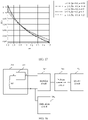
- the voltage difference ⁇ V of Vrect is 98 mV * (0.9/0.68) ⁇ 130 mV, and 130 mV > 100 mV, which satisfies an ASK communication requirement, and ⁇ V is increased from 98 mV to 130 mV when the modulation capacitance ratio ⁇ is increased.
- increasing the modulation capacitance ratio ⁇ can avoid impact of an excessively small voltage difference of Vrect on ASK communication quality, and decreasing the modulation capacitance ratio ⁇ can avoid impact of an excessively large voltage difference of Vrect on ASK communication quality.
- the modulation capacitance ratio ⁇ is 0.1, 0.25, 0.5, 0.75, and 1.0 in sequence.
- the modulation capacitance ratio ⁇ is 0.1, 0.25, 0.5, 0.75, and 1.0 in sequence.
- the scalarized operating angular frequency ⁇ n is 1.0 to 2.0, and after the coupling factor k becomes large, the scalarized operating angular frequency is 0.63 to 1.26.
- Mv decreases with the increase of ⁇ , and negative ASK modulation occurs. Therefore, in the positive ASK modulation process (the scalarized operating angular frequency is 1.05 to 1.26), increasing the modulation capacitance ratio ⁇ can increase the loop voltage gain, thereby improving the loading capability and enhancing ASK communication quality.
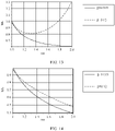
- a voltage gain curve is shown in FIG. 13 , where a horizontal axis is the scalarized operating angular frequency ⁇ n, and a vertical axis is the voltage gain Mv.
- Vrect needs to have a valid voltage difference during ASK communication.
- the voltage gain is relatively large (Mv > 0.8), and the capacitor C3 is charged during communication, but when the modulation capacitor is disconnected, the voltage gain needs to be reduced to achieve a valid voltage difference of Vrect.
- the load is insufficient, and this causes the voltage of the capacitor C3 to increase continuously, resulting in a distortion of a communication waveform.
- a voltage gain curve is shown in FIG. 14 , where a horizontal axis is the scalarized operating angular frequency con, and a vertical axis is the voltage gain Mv.
- increasing the load reduces the voltage difference of the rectified voltage Vrect during communication, and due to the increase of the load, the operating angular frequency ⁇ n decreases, and this further reduces the voltage difference of the rectified voltage Vrect, resulting in demodulation failure on the transmitting terminal.
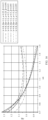
- a voltage gain curve shown in FIG. 15 is drawn, where a horizontal axis is the scalarized operating angular frequency ⁇ n, and a vertical axis is the voltage gain Mv.
- the voltage gain Mv is negatively correlated with the coupling factor k and negatively correlated with the resonant capacitance ratio ⁇ .
- the coupling factor is relatively large, the leakage inductance L1s is relatively small, and the resonant capacitor is overcompensated. In this case, the capacitance value of the resonant capacitor is relatively large, and the resonant capacitance ratio ⁇ is relatively small.
- the scalarized operating angular frequency ⁇ n 1.0 to 2.0
- An impedance characteristic in normal operation of WPC wireless charging is inductive. After the coupling factor becomes large, critical impedance (capacitive impedance and inductive impedance) occurs in normal operation, and negative ASK modulation occurs in a capacitive impedance region (overcompensation). As shown in FIG.
- the resonant capacitance ratio ⁇ is 0.25, 0.33, 0.5, 1.0, and 5 in sequence.
- the operating frequency is 100 kHz to 200 kHz.
- the coupling factor is 0.8
- the scalarized operating angular frequency ⁇ n of the system is below 1.26.
- the solutions provided in embodiments of this application mainly resolve the foregoing problems according to the following principles:
- the problem of negative ASK modulation can be resolved by optimizing the resonant capacitor C2 or the modulation capacitor of the power receiving terminal electronic device;
- the problem of the communication waveform distortion when the wireless charging system is lightly loaded can be resolved by optimizing the impedance of the power receiving terminal electronic device;
- the problem of decrease or increase of the voltage difference of the rectified voltage Vrect can be resolved by optimizing the equivalent capacitive reactance (for example, the modulation capacitance or the resonant capacitance) of the power receiving terminal electronic device.
- an electronic device provided in an embodiment of this application is described in detail as follows:
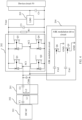
- the electronic device includes a device circuit 50, a voltage conversion circuit 203, a rectifier circuit 202, a resonant circuit 201, and a modulation circuit 204.
- An input end of the device circuit 50 is coupled to an output end of the voltage conversion circuit 203
- an input end of the voltage conversion circuit 203 is coupled to an output end of the rectifier circuit 202
- an input end of the rectifier circuit 202 is coupled to an output end of the resonant circuit 201
- the modulation circuit 204 is coupled to the input end of the rectifier circuit 202.
- the resonant circuit 201 is configured to induce an alternating magnetic field sent by a power transmitting terminal device to generate an induced alternating current; the modulation circuit 204 is configured to modulate an amplitude of the alternating current; the rectifier circuit 202 is configured to rectify the amplitude-modulated induced alternating current to generate a rectified voltage Vrect; and the voltage conversion circuit 203 is configured to convert the rectified voltage into a load voltage and output the load voltage to the device circuit 50.
- the resonant circuit 201 includes a resonant inductor L2 and a resonant capacitor control circuit ci1 connected in series to the resonant inductor L2.
- a first end of the resonant inductor L2 is coupled to the rectifier circuit 202, a second end of the resonant inductor L2 is coupled to a first end a of the resonant capacitor control circuit ci1, and a second end of the resonant capacitor control circuit ci1 is coupled to the rectifier circuit 202.
- the resonant capacitor control circuit ci1 is configured to adjust a capacitance value of a resonant capacitor connected to the resonant circuit.
- the resonant capacitor control circuit ci1 can adjust the capacitance value of the resonant capacitor connected to the resonant circuit. Therefore, with reference to the analysis of FIG. 15 , FIG. 16 , and FIG. 17 , by adjusting the capacitance value of the resonant capacitor, a resonant capacitance ratio ⁇ can be adjusted. Because a gain of the rectified voltage can be indirectly adjusted by adjusting the resonant capacitance ratio a, a problem of negative ASK modulation or decrease or increase of a voltage difference of the rectified voltage Vrect is resolved. Therefore, ASK communication quality is improved, and compatibility of the electronic device in wireless charging is improved.
- the resonant capacitor control circuit ci 1 includes a capacitance value switching network formed by at least one switch and at least one capacitor, and the resonant capacitor control circuit ci1 is configured to control a status of the switch to adjust the capacitance value of the resonant capacitor connected to the resonant circuit.
- the resonant capacitor control circuit ci1 includes an adjustable capacitor Cj, a first end of the adjustable capacitor Cj is coupled to the second end of the resonant inductor L2, and a second end of the adjustable capacitor Cj is coupled to the rectifier circuit 202.
- the capacitance value of the resonant capacitor connected to the resonant circuit can be adjusted by directly adjusting a capacitance value of the adjustable capacitor Cj.
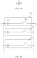
- the resonant capacitor control circuit ci1 includes at least two parallel resonant capacitor regulating branches F (F1 to Fn).
- a first end of the resonant capacitor regulating branch F1 (F2 to Fn) is coupled to the second end (node a) of the resonant inductor L2, and a second end of the resonant capacitor regulating branch F1 (F2 to Fn) is coupled to the rectifier circuit 202 (node b).
- a first switch Ka and a first capacitor Ca are connected in series on at least one resonant capacitor regulating branch F1 (F2 to Fn), and the resonant capacitor control circuit ci1 adjusts, by adjusting a status of a first switch Ka on the at least one resonant capacitor regulating branch F1 (F2 to Fn), the capacitance value of the resonant capacitor connected to the resonant circuit 201.
- the first switch Ka of the resonant capacitor regulating branch F1 is controlled to be in an on state by default.
- the first capacitor Ca on the resonant capacitor regulating branch F1 is used as the resonant capacitor, and the resonant capacitor and the resonant inductor L2 form the resonant circuit to receive power sent by a power transmitting terminal electronic device.
- the first switch Ka of the resonant capacitor regulating branch F2 may be controlled to be in an on state.
- a capacitor equivalent to the first capacitor Ca on the resonant capacitor regulating branch F1 and the first capacitor Ca on the resonant capacitor regulating branch F2 that are connected in parallel is used as the resonant capacitor, and the resonant capacitor and the resonant inductor L2 form the resonant circuit to receive power sent by the power transmitting terminal electronic device. Because the capacitance value of the resonant capacitor becomes large, the resonant capacitance ratio is reduced, and the voltage gain is increased.
- first switches Ka of more resonant capacitor regulating branches may alternatively be controlled to be turned on if the voltage gain obtained by connecting two first capacitors in parallel is still insufficient. As shown in FIG.
- one resonant capacitor regulating branch F1 includes a second capacitor Cb, a first end of the second capacitor Cb is coupled to the second end of the resonant inductor L2, and a second end of the second capacitor Cb is coupled to the rectifier circuit 202.
- a control principle of the second capacitor Cb is the same as the control of any resonant capacitor regulating branch shown in FIG. 21 .
- the second capacitor Cb is used as the resonant capacitor, and the resonant capacitor and the resonant inductor L2 form the resonant circuit to receive power sent by the power transmitting terminal electronic device.
- the first switch Ka of the resonant capacitor regulating branch F1 may be controlled to be in the on state.
- a capacitor equivalent to the second capacitor Cb and the first capacitor Ca on the resonant capacitor regulating branch F1 that are connected in parallel is used as the resonant capacitor, and the resonant capacitor and the resonant inductor L2 form the resonant circuit to receive power sent by the power transmitting terminal electronic device. Because the capacitance value of the resonant capacitor becomes large, the resonant capacitance ratio is reduced, and the voltage gain becomes large.
- the first switch Ka may be a bidirectional switch, and a current flowing in the resonant circuit 201 is in a form of an alternating current. Therefore, the current needs to be conducted from a to b or from b to a. Therefore, the first switch needs to have a bidirectional conduction function.
- the bidirectional switch may be a reverse series switching transistor. Because the switching transistor generally has a unidirectional conduction characteristic, a bidirectional conduction effect needs to be achieved by using two reverse series switching transistors.
- the switching transistor has a gate (gate, g) and a first electrode, for example, a drain (drain, d), and a second electrode, for example, a source (source, s).
- the switching transistor may be an N-type switching transistor or a P-type switching transistor.
- the first switch K1 includes a switching transistor Qs1 and a switching transistor Qs2.
- a drain (drain, d) of Qs1 is connected to a drain d of Qs2
- a source (source, s) of Qs1 is connected to the node a through the first capacitor Ca
- a source s of Qs2 is connected to the node b.
- Gates (gate, g) of Qs1 and Qs2, as gating ends of the first switch 31, are configured to receive gating signals.
- the electronic device may include a gating control circuit 207 and a drive circuit 206 shown in FIG. 22 , where the gating control circuit 207 is configured to generate a logic signal, and the drive circuit 206 may convert the logic signal into a voltage signal and provide the voltage signal as a gating signal to the gates g of Qs1 and Qs2 to control turn-on or turn-off of Qs1 and Qs2.
- a direction of a current is from d to s (an anode (anode, a) of a parasitic diode D1 is coupled to the source s of Qs1, a cathode (cathode, c) of the parasitic diode D1 is coupled to the drain d of Qs1, and a parasitic diode D2 in Qs2 is connected in the same way as the parasitic diode D1 in Qs1).
- Qs1 as an example, a conduction direction of the parasitic capacitor D1 in a freewheeling function is from s to d.
- the first switch K includes one switching transistor, a current in the direction from s to d cannot be cut off when the switching transistor is in an off state.
- a current from the node a to the node b can pass through the parasitic diode of Qs1 and the drain d and source s of Qs2 in sequence; and a current from the node b to the node a can pass through the parasitic diode of Qs2 and the drain d and source s of Qs1 in sequence.
- the resonant capacitor is connected in series in the resonant circuit, during power transmission, main power is transmitted by using the resonant capacitor. Therefore, adjusting the resonant capacitor causes system instability. Therefore, capacitive reactance of ASK modulation is usually not optimized by adjusting the resonant capacitor. However, when negative ASK modulation occurs, ASK communication fails directly. Therefore, in this application, the resonant capacitor is mainly adjusted during negative ASK modulation. With reference to the foregoing analysis of FIG. 16 , a main cause of negative ASK modulation is that the resonant capacitor is overcompensated.
- the resonant capacitor control circuit ci1 is configured to increase the capacitance value of the resonant capacitor connected to the resonant circuit, to recover positive ASK modulation of the rectified voltage.
- the scalarized operating angular frequency is 1.0 to 2.0, and after the coupling factor k becomes large, the scalarized operating angular frequency is 0.63 to 1.26.
- An impedance characteristic in normal operation of WPC wireless charging is inductive. After the coupling factor becomes large, critical impedance (capacitive impedance and inductive impedance) occurs in normal operation, and negative modulation occurs in a capacitive impedance region (overcompensation).
- a waveform graph of Vrect when the electronic device is in positive ASK modulation is shown by a waveform graph 1
- a waveform graph when the electronic device is in negative ASK modulation is shown by a stage T1 in a waveform graph 2, where a phase difference between the waveform graph of Vrect during negative ASK modulation and the waveform graph of Vrect during negative ASK modulation is 180°.
- the device circuit 50 can detect the rectified voltage Vrect.
- the resonant capacitor control circuit cil increases the capacitance value of the resonant capacitor connected to the resonant circuit 201, to recover positive modulation of the rectified voltage.
- the capacitance value of the adjustable capacitor Cj may be increased, so that the resonant capacitance ratio ⁇ is reduced and that negative ASK modulation is corrected to positive ASK modulation.
- the first switch Ka of the resonant capacitor regulating branch F1 is controlled to be in the on state by default.
- the first capacitor Ca on the resonant capacitor regulating branch F1 is used as the resonant capacitor, and the resonant capacitor and the resonant inductor L2 form the resonant circuit to receive power sent by the power transmitting terminal electronic device.
- the first switch Ka of the resonant capacitor regulating branch F2 may be controlled to be in the on state.
- the capacitor equivalent to the first capacitor Ca on the resonant capacitor regulating branch F1 and the first capacitor Ca on the resonant capacitor regulating branch F2 that are connected in parallel is used as the resonant capacitor, and the resonant capacitor and the resonant inductor L2 form the resonant circuit to receive power sent by the power transmitting terminal electronic device.
- first switches Ka of more resonant capacitor regulating branches may alternatively be controlled to be turned on if two first capacitors connected in parallel are insufficient for correcting negative ASK modulation to positive ASK modulation.
- a sequence of the gating signals of Qs1 and Qs2 is also provided.
- an objective of increasing the capacitance value of the resonant capacitor is achieved by inputting the gating signals of the sequence at the gates g of Qs1 and Qs2 of one or more resonant capacitor regulating branches.
- an electronic device includes a device circuit 50, a voltage conversion circuit 203, a rectifier circuit 202, a resonant circuit 201, and a modulation circuit 204.
- An input end of the device circuit 50 is coupled to an output end of the voltage conversion circuit 203
- an input end of the voltage conversion circuit 203 is coupled to an output end of the rectifier circuit 202
- an input end of the rectifier circuit 202 is coupled to an output end of the resonant circuit 201
- the modulation circuit 204 is coupled to the input end of the rectifier circuit 202.
- the resonant circuit 201 is configured to induce an alternating magnetic field sent by a power transmitting terminal device to generate an induced alternating current; the modulation circuit 204 is configured to modulate an amplitude of the alternating current; the rectifier circuit is configured to rectify the amplitude-modulated induced alternating current to generate a rectified voltage; and the voltage conversion circuit 203 is configured to convert the rectified voltage into a load voltage and output the load voltage to the device circuit 50.
- the electronic device further includes a load control circuit 208.
- the load control circuit 208 is coupled to the input end of the rectifier circuit 202, and the load control circuit 208 is configured to connect a resistance value to the input end of the rectifier circuit 202 when the rectified voltage is at a low level.
- the load control circuit 2 can connect the resistance value to the input end of the rectifier circuit when the rectified voltage is at the low level. Based on the analysis of FIG. 13 , a modulation capacitor is disconnected when the rectified voltage is at the low level. In this case, a voltage gain needs to be reduced. Because the resistance value is connected to the input end of the rectifier circuit, energy of the input end of the rectifier circuit can be forcibly released when the modulation capacitor is disconnected. In this way, continuous increase of a voltage of a capacitor C3 is avoided, and a modulation waveform is improved by dividing the rectified voltage. For example, low level burrs or oscillations are eliminated.
- the load control circuit 208 includes a resistance value switching network formed by at least one switch and at least one resistor, and the load control circuit 208 is configured to control a status of the switch to adjust the resistance value connected to the input end of the rectifier circuit.
- the device circuit 50 is further configured to detect power Pout corresponding to the rectified voltage Vrect and power Pri consumed by the resistance value connected by the load control circuit 208 to the input end of the rectifier circuit; and the load control circuit 208 is configured to disconnect the resistance value when it is determined that the power Pout corresponding to the rectified voltage is greater than the power Pri consumed by the resistance value.
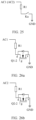
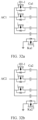
- the load control circuit 208 includes a first switch Ka and a first resistor R1, a first end of the first resistor R1 is coupled to the input end AC 1 (or AC2) of the rectifier circuit 202, a second end of the first resistor R1 is coupled to a first end of the first switch Ka, and a second end of the first switch Ka is grounded GND.
- the first switch Ka includes a switching transistor Q1-2.
- the switching transistor Q1-2 may include an N-type switching transistor or a P-type switching transistor. It can be learned from the foregoing description that when the N-type switching transistor is turned on, a direction of a current is from a drain d to a source s, and the current needs to be released to the GND through a resistor. Therefore, when the N-type switching transistor is used, the source s of the switching transistor can be directly grounded, so that floating of the source of the switching transistor is avoided. For example, the source s of the switching transistor is grounded GND.
- the source s has a fixed value, and the N-type switching transistor can be turned on as long as a voltage of a gate g is higher than a voltage of the source s.
- the circuit design is relatively simple.
- a direction of a current is from a source s to a drain d, and the current needs to be released to the GND through a resistor. Therefore, the drain d is grounded GND.
- a voltage of the source s is not fixed, and a voltage of a gate g that controls turn-on of the P-type switching transistor cannot be determined.
- FIG. 26b also shows that a first switch K in the load control circuit 208-2 connected to AC2 may include a switching transistor Q2-2 whose connection mode is similar to that of the switching transistor Q1-2 and is not described.
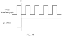
- a sequence diagram of a gating signal of Q1-2 (Q2-2) is provided.
- the first switch Ka of the load control circuit 208 is turned on (when the switching transistor Q1-2 (Q2-2) is used, the switching transistor Q1-2 (Q2-2) is controlled to be turned on by using a gating signal), and the first resistor is connected to the input end AC1 (AC2) of the rectifier circuit 202.
- the device circuit 50 detects power Pout (Vout * Iout, where Vout is an output voltage of an LDO, and Iout is an output current of the LDO) corresponding to the rectified voltage Vrect and power Pri consumed by the first resistor connected by the load control circuit 208 to the input end of the rectifier circuit.
- Pout Vout * Iout
- Iout an output current of the LDO
- the first switch Ka is turned off (when the switching transistor Q1-2 (Q2-2) is used, the switching transistor Q1-2 (Q2-2) is controlled to be turned off by using a gating signal.
- an electronic device in an example 3, as shown in FIG. 28 , includes a device circuit 50, a voltage conversion circuit 203, a rectifier circuit 202, a resonant circuit 201, and a modulation circuit 204.
- An input end of the device circuit 50 is coupled to an output end of the voltage conversion circuit 203
- an input end of the voltage conversion circuit 203 is coupled to an output end of the rectifier circuit 202
- an input end of the rectifier circuit 202 is coupled to an output end of the resonant circuit 201
- the modulation circuit 204 is coupled to the input end of the rectifier circuit 202.
- the resonant circuit 201 is configured to induce an alternating magnetic field sent by a power transmitting terminal device to generate an induced alternating current; the modulation circuit 204 is configured to modulate an amplitude of the alternating current; the rectifier circuit 202 is configured to rectify the amplitude-modulated induced alternating current to generate a rectified voltage Vrect; and the voltage conversion circuit is configured to convert the rectified voltage into a load voltage and output the load voltage to the device circuit 50.
- the modulation circuit 204 is configured to adjust a capacitance value of a modulation capacitor connected to the input end of the rectifier circuit 202.
- the solution provided in this embodiment of this application is based on a differential biphase coding scheme in which the rectifier circuit 202 includes two input ends AC1 and AC2 as shown in FIG. 4
- two modulation circuits 204 (204-1 and 204-2) are included, as shown in FIG. 28 , where the modulation circuit 204-1 is connected to the input end AC1 of the rectifier circuit 202 and the modulation circuit 204-2 is connected to the input end AC2 of the rectifier circuit 202.
- Structures of the modulation circuits connected to the two input ends AC1 and AC2 are the same.
- the two modulation circuits 204-1 and 204-2 may be integrated into one modulation circuit, as shown in FIG. 4 .
- the modulation circuit can adjust the capacitance value of the modulation capacitor connected to the input end of the rectifier circuit, a value of a modulation capacitance ratio can be adjusted. Because a gain of the rectified voltage can be indirectly adjusted by adjusting the value of the modulation capacitance ratio, a problem of negative ASK modulation or decrease or increase of a voltage difference of the rectified voltage Vrect is resolved. Therefore, ASK communication quality is improved, and compatibility of the electronic device in wireless charging is improved.
- the modulation circuit includes a capacitance value switching network formed by at least one switch and at least one capacitor, and the modulation circuit is configured to control a status of the switch to adjust the capacitance value of the modulation capacitor connected to the input end of the rectifier circuit.
- the modulation circuit 204 includes a first switch Ka and an adjustable capacitor Cj, a first end of the adjustable capacitor Cj is coupled to the input end AC1 (AC2) of the rectifier circuit 202, a second end of the adjustable capacitor Ci is coupled to a first end of the first switch Ka, and a second end of the first switch Ka is coupled to the ground GND.
- the first switch Ka may be a switching transistor Q1 -1, such as an N-type switching transistor or a P-type switching transistor.
- the N-type switching transistor may be preferably used as the first switch Ka, as described above.
- the modulation circuit 204 includes a first switch Ka and at least two parallel modulation capacitor branches Y (Y1 to Yn), a first end of the modulation capacitor branch Y (Y1 to Yn) is coupled to the input end AC1 of the rectifier circuit 202, a second end of the modulation capacitor branch Y (Y1 to Yn) is coupled to a first end of the first switch Ka, and a second end of the first switch Ka is coupled to the ground GND.
- Any modulation capacitor branch Y (Y1 to Yn) includes a first capacitor Ca and a second switch Kb, a first end of the second switch Kb is coupled to the input end of the rectifier circuit 202, a second end of the second switch Kb is coupled to a first end of the first capacitor Ca, and a second end of the first capacitor Ca is coupled to the first end of the first switch Ka.
- the modulation circuit 204 adjusts, by adjusting a status of the second switch Kb on the at least one modulation capacitor branch Y (Y1 to Yn), the capacitance value of the modulation capacitor connected to the input end of the rectifier circuit 204.
- the second switch Kb of the modulation capacitor branch Y1 is controlled to be in an on state by default, and a voltage gain needs to be increased.
- the second switch Kb of the modulation capacitor branch Y2 is controlled to be in an on state.
- the modulation capacitor connected to the input end AC1 (AC2) of the rectifier circuit 202 is a capacitor equivalent to the first capacitor Ca on the modulation capacitor branch Y1 and the first capacitor Ca on Y2 that are connected in parallel. If the voltage gain needs to be increased, the second switch Kb of the modulation capacitor branch Y3 continues to be controlled to be in an on state.
- the modulation capacitor connected to the input end AC1 (AC2) of the rectifier circuit 202 is a resistor equivalent to three first capacitors Ca on the modulation capacitor branches Y1, Y2, and Y3 that are connected in parallel, thereby increasing the capacitance value of the modulation capacitor connected to the input end of the rectifier circuit 204.
- the second switch Kb of the modulation capacitor branch Y3 can be controlled to be in an off state, to reduce the capacitance value of the modulation capacitor connected to the input end of the rectifier circuit 204.
- the foregoing is merely an example, and it is also possible to select to control two or more modulation capacitor branches Y at the same time based on an actual situation.
- a second capacitor Cb is connected in series on any modulation capacitor branch Y In this way, Cb is equivalent to Cm1 (Cm2) in FIG. 5 .
- a control principle of the second capacitor Cb is the same as the control of any modulation capacitor branch Y shown in FIG. 31 .
- the second capacitor Cb is used as the modulation capacitor to connect to the input end AC1 (AC2) of the rectifier circuit 202.
- AC2 AC1
- the second switch Kb on any modulation capacitor branch Y is controlled to be turned on.
- the second switch Kb currently in the on state on any modulation capacitor branch Y is controlled to be turned off.
- the second switch Kb in the modulation circuit 204-1 may be a switching transistor Q1-1, where a first capacitor Ca (Ca1) and a first switch Ka (Ka1) are also shown in FIG. 32a .
- the second switch Kb in the modulation circuit 204-2 may be a switching transistor Q2-1, where a first capacitor Ca (Ca2) and a first switch Ka (Ka2) are also shown in FIG. 32b .
- the switching transistor Q1-1 and the switching transistor Q2-1 may be N-type switching transistors or P-type switching transistors. For details about controlling a status of a switching transistor by using a gating signal, refer to the description in the example 1. Details are not described herein again.
- the resonant capacitor is connected in series in the resonant circuit, during power transmission, main power is transmitted by using the resonant capacitor. Therefore, adjusting the resonant capacitor causes system instability. Therefore, capacitive reactance of ASK modulation is usually not optimized by adjusting the resonant capacitor. However, when negative ASK modulation occurs, ASK communication fails directly. Therefore, in this application, the resonant capacitor is mainly adjusted during negative ASK modulation. With reference to the analysis of FIG. 15 , a main cause of negative ASK modulation is that the resonant capacitor is overcompensated. Although adjusting the resonant capacitor can also optimize the voltage difference of Vrect, considering impact of the adjustment on system stability, the voltage difference of the rectified voltage Vrect is mainly optimized by adjusting the modulation capacitor in this embodiment of this application.
- the voltage difference of the rectified voltage Vrect when the voltage difference of the rectified voltage Vrect is relatively small due to abnormal ASK modulation when the electronic device is in a full load or heavy load state, or the voltage difference of the rectified voltage Vrect is excessively large and affects communication quality, the voltage difference of the rectified voltage Vrect can be restored to a normal range by adjusting the modulation capacitor.
- the device circuit 50 is further configured to detect the rectified voltage; and when a maximum voltage difference ⁇ Vrect of the rectified voltage is less than or equal to a first threshold voltage Vset-th1 and the rectified voltage is at the low level, the modulation circuit 204 is configured to increase the capacitance value of the modulation capacitor connected to the input end of the rectifier circuit; or when a maximum voltage difference of the rectified voltage is greater than or equal to a second threshold voltage Vset-th2 and the rectified voltage is at the low level, the modulation circuit is configured to reduce the capacitance value of the modulation capacitor connected to the input end of the rectifier circuit, where Vset-th2 is greater than Vset-th1.
- the vset-th1 can determine a smallest value of ⁇ Vrect that does not affect ASK communication quality.
- the Vset-th2 can determine a largest value of ⁇ Vrect that does not affect ASK communication quality.
- the capacitance value of the modulation capacitor connected to the input end of the rectifier circuit is increased. Because the capacitance value of the modulation capacitor is increased, when the modulation waveform is at the high level, the amplitude of Vrect is higher, so that ⁇ Vrect is increased. Conversely, if the capacitance value of the modulation capacitor is decreased, when the modulation waveform is at the high level, the amplitude of Vrect is reduced, so that ⁇ Vrect is decreased.
- the capacitance value of the adjustable capacitor Cj when ⁇ Vrect ⁇ Vset-th1, the capacitance value of the adjustable capacitor Cj can be increased, and when ⁇ Vrect ⁇ Vset-th2, the capacitance value of the adjustable capacitor Cj can be decreased.
- the second switch Kb of the modulation capacitor branch Y1 is controlled to be in the on state by default.
- the second switch Kb of the modulation capacitor branch Y2 is controlled to be in the on state.
- the modulation capacitor connected to the input end AC1 (AC2) of the rectifier circuit 202 is a capacitor equivalent to the first capacitor Ca on the modulation capacitor branch Y1 and the first capacitor Ca on Y2 that are connected in parallel. If ⁇ Vrect ⁇ Vset-th1, the second switch Kb of the modulation capacitor branch Y3 continues to be controlled to be in the on state. In this way, the modulation capacitor connected to the input end AC1 (AC2) of the rectifier circuit 202 is a resistor equivalent to three first capacitors Ca on the modulation capacitor branches Y1, Y2, and Y3 that are connected in parallel, thereby increasing the capacitance value of the modulation capacitor connected to the input end of the rectifier circuit 204.
- the second switch Kb of the modulation capacitor branch Y3 can be controlled to be in the off state, to reduce the capacitance value of the modulation capacitor connected to the input end of the rectifier circuit 204.
- the foregoing is merely an example, and it is also possible to select to control two or more modulation capacitor branches Y at the same time based on an actual value of ⁇ Vrect. This is not specifically limited in this application.
- a waveform graph of a gating signal when Q1-1 (Q2-1) is an N-type switching transistor is also provided.
- the foregoing examples 1, 2, and 3 provide three electronic devices. However, improvement solutions included in the foregoing three electronic devices may work independently, or two or all of the improvement solutions may be disposed in the same electronic device.
- an embodiment of this application further provides a control method for an electronic device. With reference to FIG. 34A and FIG. 34B , the method specifically includes the following steps.
- a device circuit detects a rectified voltage, and determines whether negative ASK modulation of the rectified voltage occurs.
- the electronic device After the electronic device starts communication and establishes wireless charging power transmission, the electronic device first determines whether negative ASK modulation occurs on the electronic device. A reason is that if negative ASK modulation of the rectified voltage occurs, the electronic device directly stops power transmission. When the device circuit determines that negative ASK modulation of the rectified voltage occurs, the process goes to step 402. If negative ASK modulation of the rectified voltage does not occur, the process goes to step 403.
- a resonant capacitor control circuit adjusts a capacitance value of a resonant capacitor connected to a resonant circuit.
- step 401 If positive ASK modulation of the rectified voltage is recovered by adjusting the capacitance value of the resonant capacitor connected to the resonant circuit, the process goes to step 401.
- a specific method for adjusting the capacitance value of the resonant capacitor connected to the resonant circuit refer to the description in the foregoing example 1.
- the resonant capacitor control circuit increases the capacitance value of the resonant capacitor connected to the resonant circuit. Details are not described herein again. Otherwise, the electronic device ends power transmission.
- a load control circuit connects a resistance value to an input end of a rectifier circuit when the rectified voltage is at a low level.
- the load control circuit connects the resistance value to the input end of the rectifier circuit when the rectified voltage is at the low level (which may be, for example, a first resistance value), to avoid a waveform distortion when the rectified voltage is at the low level.
- the low level which may be, for example, a first resistance value
- the device circuit is further configured to detect power corresponding to the rectified voltage and power consumed by the resistance value connected by the load control circuit to the input end of the rectifier circuit; and determine whether the power corresponding to the rectified voltage is greater than the power consumed by the resistance value.
- step 405 When the power corresponding to the rectified voltage is greater than the power consumed by the resistance value, the process goes to step 405, or when the power corresponding to the rectified voltage is less than or equal to the power consumed by the resistance value, the process goes to step 406.
- the load control circuit disconnects the resistance value.
- the load control circuit keeps connecting the resistance value to the input end of the rectifier circuit when the rectified voltage is at the low level.
- a modulation circuit adjusts a capacitance value of a modulation capacitor connected to the input end of the rectifier circuit.
- the device circuit detects the rectified voltage and determines whether a maximum voltage difference of the rectified voltage is greater than or equal to a second threshold voltage.
- step 408 When the maximum voltage difference of the rectified voltage is greater than or equal to the second threshold voltage, the process goes to step 408; otherwise, the process goes to step 409.
- the modulation circuit reduces the capacitance value of the modulation capacitor connected to the input end of the rectifier circuit.
- the electronic device After the capacitance value of the modulation capacitor connected to the input end of the rectifier circuit is adjusted to make the maximum voltage difference of the rectified voltage less than the second threshold voltage, the electronic device normally performs power transmission until the end.
- the device circuit detects the rectified voltage and determines whether the maximum voltage difference of the rectified voltage is less than or equal to a first threshold voltage.
- the process goes to step 410; otherwise, the electronic device normally performs power transmission until the end.
- the modulation circuit increases the capacitance value of the modulation capacitor connected to the input end of the rectifier circuit.
- the electronic device After the capacitance value of the modulation capacitor connected to the input end of the rectifier circuit is adjusted to make the maximum voltage difference of the rectified voltage greater than the first threshold voltage, the electronic device normally performs power transmission until the end.
- step 407 may be performed after step 403, or step 403 is performed after step 407. Specifically, which of steps 403 and 407 first satisfies a corresponding determining condition is considered.
- step 403 usually satisfies the determining condition first
- step 407 usually satisfies the corresponding determining condition only in a full load or heavy load condition in the power transmission process.
- the electronic device includes the resonant circuit 201 provided in the example 1, the load control circuit 208 provided in the example 2, and the modulation circuit 202 provided in the example 3, and the resonant circuit includes the resonant capacitor control circuit provided in FIG. 22 (Cb in FIG. 22 may be the resonant capacitor (C2 in FIG. 4 )), and the modulation circuit 202 includes the modulation circuit provided in FIG. 31 (Cb in FIG. 31 may be the modulation capacitor (Cm1 (Cm2) in FIG.
- the electronic device satisfies the following operating conditions, and clears the control method logic provided in embodiments of this application, for example, with regard to the solution provided in the example 1, stops the control of the first switch Ka on the resonant capacitor regulating branch, keeps the first switch Ka on the resonant capacitor regulating branch in the off state, and can connect only the second capacitor Cb in FIG.
- Operating condition 2 The electronic device is in a critical region of ping (a detection waiting stage, in which a transmitting terminal detects whether a potential receiving terminal electronic device is a power receiver or whether a power receiver requires power transmission), and does not need to have good ASK communication with the transmitting terminal; and the electronic device is located in the critical region of ping. In this case, power transmission efficiency is very low. In this case, if communication between the terminal device and the transmitting terminal is forcibly optimized, it is a waste of electric energy to maintain power transmission. Therefore, the electronic device is not controlled in the critical region of ping.
- Operating condition 3 The electronic device is under overvoltage protection, overcurrent protection, overtemperature protection, or the like.
- the operating condition 1 and the operating condition 3 can be determined by the device circuit 50 based on a current running state of the device.
- the operating condition 2 needs to be determined by the device circuit 50 based on operating parameters collected for the rectifier circuit and the voltage conversion circuit. Specifically, for a variable-frequency system, when Vout * Iout ⁇ Pout_Th && Freq_op ⁇ Freq _th, it is determined that the operating condition 2 is satisfied; and for a fixed-frequency system, when Vrect ⁇ Vrect_th && Thold ⁇ Tth, it is determined that the operating condition 2 is satisfied.
- Vout is an output voltage of the IDO
- Iout is an output current of the IDO
- Pout_Th is an output power threshold
- Freq_op is an operating frequency of the power receiving terminal electronic device
- Freq_th is a frequency threshold.
- Freq_op in the Qi specification is generally 100-200 kHz, and Freq_th may be set to 110 kHz or the like based on an actual situation.
- Thold is duration when Vrect ⁇ Vrect_th. Therefore, the fixed-frequency system satisfies the second operating condition only when Vrect ⁇ Vrect_th within a range of Thold ⁇ Tth.
Landscapes
- Engineering & Computer Science (AREA)
- Power Engineering (AREA)
- Computer Networks & Wireless Communication (AREA)
- Signal Processing (AREA)
- Charge And Discharge Circuits For Batteries Or The Like (AREA)
Abstract
Description
- This application claims priority to
Chinese Patent Application No. 202010507482.5, filed with the China National Intellectual Property Administration on June 5, 2020 - This application relates to the field of wireless charging technologies, and in particular, to an electronic device and a control method for the electronic device.
- A wireless charging technology is to induce energy from a primary coil of a power transmitting terminal device to a secondary coil of a power receiving terminal device through near-field electromagnetic induction, thereby completing power transmission. Usually, to achieve compatibility of various devices, a power receiving terminal device in wireless charging needs to be adapted to power transmitting terminal devices that satisfy a Qi standard, including a mobile phone, a tablet, a charging chassis, and the like supporting a reverse charging function. Transmitting terminals of different brands use different rectifier circuit (for example, alternating current (alternating current, AC) to direct current (direct current, DC) conversion, AC/DC) topologies, modulation modes, circuit parameters, operating frequencies, and control logic. Therefore, for different power transmitting terminal devices, the power receiving terminal device may not satisfy specifications of the Qi standard.
- In a power transmission process of wireless charging, communication between the power transmitting terminal device and the power receiving terminal device in wireless charging supports ASK (amplitude shift keying, amplitude shift keying) modulation. ASK modulation is to modulate transmit power signal load through reverse reflection to achieve an objective of information transmission. As the load in the ASK modulation changes, a power signal envelope alternately appears to be in a high (high) or low (low) state. As specified in the Qi (an identity of the Wireless Power Consortium) protocol, if a change of a high/low state current is greater than 15 mA or a change of a high/low voltage is greater than 200 mV, information transmitted by a power signal envelope is valid; or if a change of a high/low state current is less than 8 mA or a change of a voltage is less than 100 mV, information transmitted by a power signal envelope is invalid. Therefore, when a load impedance change causes a power (or power) signal distortion and an amplitude of a distorted voltage or current exceeds a data validity upper limit, incorrect demodulation by an ASK demodulation circuit is caused, and further, power transmission is interrupted. When the power signal distortion cycle approaches an ASK modulation cycle fclk = 2 kHz, an electronic device cannot be wirelessly charged.
- Embodiments of this application provide an electronic device and a control method for the electronic device, to improve compatibility of a power receiving terminal device in wireless charging with a power transmitting terminal device by improving ASK communication quality.
- According to a first aspect, an electronic device is provided. The electronic device includes a device circuit, a voltage conversion circuit, a rectifier circuit, a resonant circuit, and a modulation circuit. An input end of the device circuit is coupled to an output end of the voltage conversion circuit, an input end of the voltage conversion circuit is coupled to an output end of the rectifier circuit, an input end of the rectifier circuit is coupled to an output end of the resonant circuit, and the modulation circuit is coupled to the input end of the rectifier circuit. The resonant circuit is configured to induce an alternating magnetic field sent by a power transmitting terminal device to generate an induced alternating current; the modulation circuit is configured to modulate an amplitude of the induced alternating current; the rectifier circuit is configured to rectify the amplitude-modulated induced alternating current to generate a rectified voltage; and the voltage conversion circuit is configured to convert the rectified voltage into a load voltage and output the load voltage to the device circuit. In addition, the resonant circuit includes a resonant inductor and a resonant capacitor control circuit connected in series to the resonant inductor. A first end of the resonant inductor is coupled to the rectifier circuit, a second end of the resonant inductor is coupled to a first end of the resonant capacitor control circuit, and a second end of the resonant capacitor control circuit is coupled to the rectifier circuit. The resonant capacitor control circuit is configured to adjust a capacitance value of a resonant capacitor connected to the resonant circuit. In this example, the resonant capacitor control circuit can adjust the capacitance value of the resonant capacitor connected to the resonant circuit. Therefore, by adjusting the capacitance value of the resonant capacitor, a gain of the rectified voltage can be indirectly adjusted by adjusting the resonant capacitor, so that a problem of negative ASK modulation or decrease or increase of a voltage difference of the rectified voltage is resolved. Therefore, ASK communication quality is improved, and compatibility of the electronic device in wireless charging is improved.
- In a possible design, an implementation of the resonant capacitor control circuit is provided. The resonant capacitor control circuit includes a capacitance value switching network formed by at least one switch and at least one capacitor, and the resonant capacitor control circuit is configured to control a status of the switch to adjust the capacitance value of the resonant capacitor connected to the resonant circuit.
- In a possible design, another implementation of the resonant capacitor control circuit is provided. The resonant capacitor control circuit includes an adjustable capacitor, a first end of the adjustable capacitor is coupled to the second end of the resonant inductor, and a second end of the adjustable capacitor is coupled to the rectifier circuit.
- In a possible design, still another implementation of the resonant capacitor control circuit is provided. The resonant capacitor control circuit includes at least two parallel resonant capacitor regulating branches. A first end of the resonant capacitor regulating branch is coupled to the second end of the resonant inductor, and a second end of the resonant capacitor regulating branch is coupled to the rectifier circuit. A first switch and a first capacitor are connected in series on at least one resonant capacitor regulating branch, and the resonant capacitor control circuit adjusts, by adjusting a status of a first switch on the at least one resonant capacitor regulating branch, the capacitance value of the resonant capacitor connected to the resonant circuit. One resonant capacitor regulating branch includes a second capacitor, a first end of the second capacitor is coupled to the second end of the resonant inductor, and a second end of the second capacitor is coupled to the rectifier circuit.
- In a possible design, the first switch includes a bidirectional switching transistor.
- In a possible design, the device circuit is further configured to detect the rectified voltage. When negative modulation of the rectified voltage occurs, the resonant capacitor control circuit increases the capacitance value of the resonant capacitor connected to the resonant circuit, to recover positive modulation of the rectified voltage. Because the resonant capacitor is connected in series in the resonant circuit, during power transmission, main power is transmitted by using the resonant capacitor. Therefore, adjusting the resonant capacitor causes system instability. Therefore, capacitive reactance of ASK modulation is usually not optimized by adjusting the resonant capacitor. However, when negative ASK modulation occurs, ASK communication fails directly. Therefore, in this embodiment of this application, the resonant capacitor is mainly adjusted during negative ASK modulation.
- In a possible design, the electronic device further includes a load control circuit. The load control circuit is coupled to the input end of the rectifier circuit, and the load control circuit is configured to connect a resistance value to the input end of the rectifier circuit when the rectified voltage is at a low level. In this example, because the load control circuit is coupled to the input end of the rectifier circuit, the load control circuit can connect the resistance value to the input end of the rectifier circuit when the rectified voltage is at the low level, and a modulation capacitor is disconnected when the rectified voltage is at the low level. In this case, a voltage gain needs to be reduced. Because the resistance value is connected to the input end of the rectifier circuit, energy of the input end of the rectifier circuit can be forcibly released when the modulation capacitor is disconnected. In this way, continuous increase of a voltage of a capacitor is avoided, and a modulation waveform is improved by dividing the rectified voltage. For example, low level burrs or oscillations are eliminated.
- In a possible design, the device circuit is further configured to detect power corresponding to the rectified voltage and power consumed by the resistance value connected by the load control circuit to the input end of the rectifier circuit; and the load control circuit is configured to disconnect the resistance value when it is determined that the power corresponding to the rectified voltage is greater than the power consumed by the resistance value.
- In a possible design, the electronic device further includes: the modulation circuit is configured to adjust a capacitance value of a modulation capacitor connected to the input end of the rectifier circuit. The modulation circuit can adjust the capacitance value of the modulation capacitor connected to the input end of the rectifier circuit, and the gain of the rectified voltage can be indirectly adjusted by adjusting the value of the modulation capacitor, so that the problem of negative ASK modulation or decrease or increase of the voltage difference of the rectified voltage Vrect is resolved. Therefore, ASK communication quality is improved, and compatibility of the electronic device in wireless charging is improved.
- In a possible design, the device circuit is further configured to detect the rectified voltage; and when a maximum voltage difference of the rectified voltage is less than or equal to a first threshold voltage and the rectified voltage is at the low level, the modulation circuit is configured to increase the capacitance value of the modulation capacitor connected to the input end of the rectifier circuit; or when a maximum voltage difference of the rectified voltage is greater than or equal to a second threshold voltage and the rectified voltage is at the low level, the modulation circuit is configured to reduce the capacitance value of the modulation capacitor connected to the input end of the rectifier circuit, where the second threshold voltage is greater than the first threshold voltage. Because the resonant capacitor is connected in series in the resonant circuit, during power transmission, main power is transmitted by using the resonant capacitor. Therefore, adjusting the resonant capacitor causes system instability. Therefore, capacitive reactance of ASK modulation is usually not optimized by adjusting the resonant capacitor. However, when negative ASK modulation occurs, ASK communication fails directly. Therefore, in this application, the resonant capacitor is mainly adjusted during negative ASK modulation. A main cause of negative ASK modulation is that the resonant capacitor is overcompensated. Although adjusting the resonant capacitor can also optimize the voltage difference of the rectified voltage, considering impact of the adjustment on system stability, the voltage difference of the rectified voltage is mainly optimized by adjusting the modulation capacitor in this embodiment of this application. According to a second aspect, an electronic device is provided. The electronic device includes a device circuit, a voltage conversion circuit, a rectifier circuit, a resonant circuit, and a modulation circuit. An input end of the device circuit is coupled to an output end of the voltage conversion circuit, an input end of the voltage conversion circuit is coupled to an output end of the rectifier circuit, an input end of the rectifier circuit is coupled to an output end of the resonant circuit, and the modulation circuit is coupled to the input end of the rectifier circuit. The resonant circuit is configured to induce an alternating magnetic field sent by a power transmitting terminal device to generate an induced alternating current; the modulation circuit is configured to modulate an amplitude of the alternating current; the rectifier circuit is configured to rectify the amplitude-modulated induced alternating current to generate a rectified voltage; and the voltage conversion circuit is configured to convert the rectified voltage into a load voltage and output the load voltage to the device circuit. The electronic device further includes a load control circuit. The load control circuit is coupled to the input end of the rectifier circuit, and the load control circuit is configured to connect a resistance value to the input end of the rectifier circuit when the rectified voltage is at a low level. In this example, because the load control circuit is coupled to the input end of the rectifier circuit, the load control circuit can connect the resistance value to the input end of the rectifier circuit when the rectified voltage is at the low level, and a modulation capacitor is disconnected when the rectified voltage is at the low level. In this case, a voltage gain needs to be reduced. Because the resistance value is connected to the input end of the rectifier circuit, energy of the input end of the rectifier circuit can be forcibly released when the modulation capacitor is disconnected. In this way, continuous increase of a voltage of a capacitor is avoided, and a modulation waveform is improved by dividing the rectified voltage. For example, low level burrs or oscillations are eliminated.
- In a possible design, an implementation of the load control circuit is provided. The load control circuit includes a resistance value switching network formed by at least one switch and at least one resistor, and the load control circuit is configured to control a status of the switch to adjust the resistance value connected to the input end of the rectifier circuit.
- In a possible design, another implementation of the load control circuit is provided. The load control circuit includes a first switch and a first resistor, a first end of the first resistor is coupled to the input end of the rectifier circuit, a second end of the first resistor is coupled to a first end of the first switch, and a second end of the first switch is grounded.
- In a possible design, the device circuit is further configured to detect power corresponding to the rectified voltage and power consumed by the resistance value connected by the load control circuit to the input end of the rectifier circuit; and the load control circuit is configured to disconnect the resistance value when it is determined that the power corresponding to the rectified voltage is greater than the power consumed by the resistance value.
- According to a third aspect, an electronic device is provided. The electronic device includes a device circuit, a voltage conversion circuit, a rectifier circuit, a resonant circuit, and a modulation circuit. An input end of the device circuit is coupled to an output end of the voltage conversion circuit, an input end of the voltage conversion circuit is coupled to an output end of the rectifier circuit, an input end of the rectifier circuit is coupled to an output end of the resonant circuit, and the modulation circuit is coupled to the input end of the rectifier circuit. The resonant circuit is configured to induce an alternating magnetic field sent by a power transmitting terminal device to generate an induced alternating current; the modulation circuit is configured to modulate an amplitude of the alternating current; the rectifier circuit is configured to rectify the amplitude-modulated induced alternating current to generate a rectified voltage; the voltage conversion circuit is configured to convert the rectified voltage into a load voltage and output the load voltage to the device circuit; and the modulation circuit is configured to adjust a capacitance value of a modulation capacitor connected to the input end of the rectifier circuit. The modulation circuit can adjust the capacitance value of the modulation capacitor connected to the input end of the rectifier circuit, and a gain of the rectified voltage can be indirectly adjusted by adjusting the value of the modulation capacitor, so that a problem of negative ASK modulation or decrease or increase of a voltage difference of the rectified voltage Vrect is resolved. Therefore, ASK communication quality is improved, and compatibility of the electronic device in wireless charging is improved.
- In a possible design, an implementation of the modulation circuit is provided. The modulation circuit includes a capacitance value switching network formed by at least one switch and at least one capacitor, and the modulation circuit is configured to control a status of the switch to adjust the capacitance value of the modulation capacitor connected to the input end of the rectifier circuit.
- In a possible design, another implementation of the modulation circuit is provided. The modulation circuit includes a first switch and an adjustable capacitor, a first end of the adjustable capacitor is coupled to the input end of the rectifier circuit, a second end of the adjustable capacitor is coupled to a first end of the first switch, and a second end of the first switch is coupled to the ground.
- In a possible design, still another implementation of the modulation circuit is provided. The modulation circuit includes a first switch and at least two parallel modulation capacitor branches, a first end of the modulation capacitor branch is coupled to the input end of the rectifier circuit, a second end of the modulation capacitor branch is coupled to a first end of the first switch, and a second end of the first switch is coupled to the ground. The modulation capacitor branch includes a first capacitor and a second switch, a first end of the second switch is coupled to the input end of the rectifier circuit, a second end of the second switch is coupled to a first end of the first capacitor, and a second end of the first capacitor is coupled to the first end of the first switch. The modulation circuit adjusts, by adjusting a status of the second switch on the at least one modulation capacitor branch, the capacitance value of the modulation capacitor connected to the input end of the rectifier circuit. A second capacitor is connected in series on one modulation capacitor branch.
- In a possible design, the device circuit is further configured to detect the rectified voltage; and when a maximum voltage difference of the rectified voltage is less than or equal to a first threshold voltage and the rectified voltage is at a low level, the modulation circuit is configured to increase the capacitance value of the modulation capacitor connected to the input end of the rectifier circuit; or when a maximum voltage difference of the rectified voltage is greater than or equal to a second threshold voltage and the rectified voltage is at a low level, the modulation circuit is configured to reduce the capacitance value of the modulation capacitor connected to the input end of the rectifier circuit, where the second threshold voltage is greater than the first threshold voltage. Because the resonant capacitor is connected in series in the resonant circuit, during power transmission, main power is transmitted by using the resonant capacitor. Therefore, adjusting the resonant capacitor causes system instability. Therefore, capacitive reactance of ASK modulation is usually not optimized by adjusting the resonant capacitor. However, when negative ASK modulation occurs, ASK communication fails directly. Therefore, in this application, the resonant capacitor is mainly adjusted during negative ASK modulation. A main cause of negative ASK modulation is that the resonant capacitor is overcompensated. Although adjusting the resonant capacitor can also optimize the voltage difference of the rectified voltage, considering impact of the adjustment on system stability, the voltage difference of the rectified voltage is mainly optimized by adjusting the modulation capacitor in this embodiment of this application. According to a fourth aspect, a control method for the electronic device provided in the first aspect is provided. A resonant circuit of the electronic device includes a resonant inductor and a resonant capacitor control circuit connected in series to the resonant inductor. The control method for the electronic device includes: a device circuit detects a rectified voltage, and when negative modulation of the rectified voltage occurs, the resonant capacitor control circuit adjusts a capacitance value of a resonant capacitor connected to the resonant circuit, to recover positive modulation of the rectified voltage.
- In a possible design, that the resonant capacitor control circuit adjusts a capacitance value of a resonant capacitor connected to the resonant circuit includes: the resonant capacitor control circuit increases the capacitance value of the resonant capacitor connected to the resonant circuit.
- In a possible design, the electronic device further includes a load control circuit; and when the rectified voltage is modulated by positive modulation, the control method includes: the load control circuit connects a resistance value to an input end of the rectifier circuit when the rectified voltage is at a low level.
- In a possible design, the control method further includes: power corresponding to the rectified voltage and power consumed by the resistance value connected by the load control circuit to the input end of the rectifier circuit are detected; and the load control circuit disconnects the resistance value when it is determined that the power corresponding to the rectified voltage is greater than the power consumed by the resistance value.
- In a possible design, when the rectified voltage is modulated by positive modulation, the control method further includes: when a maximum voltage difference of the rectified voltage is less than or equal to a first threshold voltage and the rectified voltage is at the low level, a modulation circuit increases a capacitance value of a modulation capacitor connected to the input end of the rectifier circuit; or when a maximum voltage difference of the rectified voltage is greater than or equal to a second threshold voltage and the rectified voltage is at the low level, a modulation circuit reduces a capacitance value of a modulation capacitor connected to the input end of the rectifier circuit, where the second threshold voltage is greater than the first threshold voltage.
- For technical effects brought by any design in the fourth aspect, refer to technical effects brought by different designs in the first aspect. Details are not described herein again.
-
-
FIG. 1 is a schematic diagram of a structure of a wireless charging system according to an embodiment of this application; -
FIG. 2 is a schematic diagram of a structure of an electronic device according to an embodiment of this application; -
FIG. 3 is a schematic diagram of a structure of a wireless charging system according to another embodiment of this application; -
FIG. 4 is a schematic diagram of a structure of a wireless charging system according to still another embodiment of this application; -
FIG. 5 is a schematic diagram of a modulation waveform according to an embodiment of this application; -
FIG. 6 is a schematic diagram of a structure of an ASK modulation circuit according to an embodiment of this application; -
FIG. 7 is a schematic diagram of a structure of an ASK modulation circuit according to another embodiment of this application; -
FIG. 8 is a schematic diagram of a modulation waveform according to another embodiment of this application; -
FIG. 9 is a schematic diagram of an equivalent circuit of the wireless charging system shown inFIG. 4 according to an embodiment of this application; -
FIG. 10 is a schematic diagram of a voltage gain curve of a wireless charging system according to an embodiment of this application; -
FIG. 11 is a schematic diagram of a voltage gain curve of a wireless charging system according to another embodiment of this application; -
FIG. 12 is a schematic diagram of a voltage gain curve of a wireless charging system according to still another embodiment of this application; -
FIG. 13 is a schematic diagram of a voltage gain curve of a wireless charging system according to yet another embodiment of this application; -
FIG. 14 is a schematic diagram of a voltage gain curve of a wireless charging system according to another embodiment of this application; -
FIG. 15 is a schematic diagram of a voltage gain curve of a wireless charging system according to still another embodiment of this application; -
FIG. 16 is a schematic diagram of a voltage gain curve of a wireless charging system according to yet another embodiment of this application; -
FIG. 17 is a schematic diagram of a voltage gain curve of a wireless charging system according to another embodiment of this application; -
FIG. 18 is a schematic diagram of a structure of an electronic device according to an embodiment of this application; -
FIG. 19 is a schematic diagram of a structure of a resonant capacitor control circuit according to an embodiment of this application; -
FIG. 20 is a schematic diagram of a structure of a resonant capacitor control circuit according to another embodiment of this application; -
FIG. 21 is a schematic diagram of a structure of a resonant capacitor control circuit according to still another embodiment of this application; -
FIG. 22 is a schematic diagram of a structure of a first switch according to an embodiment of this application; -
FIG. 23 is a waveform graph of Vrect according to an embodiment of this application; -
FIG. 24 is a schematic diagram of a structure of an electronic device according to another embodiment of this application; -
FIG. 25 is a schematic diagram of a structure of a load control circuit according to an embodiment of this application; -
FIG. 26a is a schematic diagram of a structure of a load control circuit according to another embodiment of this application; -
FIG. 26b is a schematic diagram of a structure of a load control circuit according to still another embodiment of this application; -
FIG. 27 is a sequence diagram of a Q1-2 (Q2-2) gating signal according to an embodiment of this application; -
FIG. 28 is a schematic diagram of a structure of an electronic device according to still another embodiment of this application; -
FIG. 29 is a schematic diagram of a structure of a modulation circuit according to an embodiment of this application; -
FIG. 30 is a schematic diagram of a structure of a modulation circuit according to another embodiment of this application; -
FIG. 31 is a schematic diagram of a structure of a modulation circuit according to still another embodiment of this application; -
FIG. 32a is a schematic diagram of a structure of a modulation circuit according to yet another embodiment of this application; -
FIG. 32b is a schematic diagram of a structure of a modulation circuit according to another embodiment of this application; -
FIG. 33 is a waveform graph of a gating signal of Q1-1 (Q2-1) according to an embodiment of this application; and -
FIG. 34A andFIG. 34B are a schematic flowchart of a control method for an electronic device according to an embodiment of this application. - The following describes the technical solutions in embodiments of this application with reference to the accompanying drawings in embodiments of this application. It is clear that the described embodiments are merely some rather than all of embodiments of this application.
- The terms "first" and "second" mentioned below are merely intended for a purpose of description, and shall not be understood as an indication or implication of relative importance or implicit indication of a quantity of indicated technical features. Therefore, a feature limited by "first" or "second" may explicitly indicate or implicitly include one or more such features. In the description of embodiments of this application, unless otherwise stated, "a plurality of" means two or more.
- In addition, in embodiments of this application, directional terms such as "up", "down", "left", and "right" may include but are not limited to those defined relative to directions in which components are placed in the accompanying drawings. It should be understood that the directional terms may be relative concepts. The directional terms are used for relative description and clarification, and may vary accordingly depending on changes of the directions in which the components are placed in the accompanying drawings.
- In the description of embodiments of this application, unless otherwise specified and defined explicitly, the terms "connection" should be understood in a broad sense. For example, the "connection" may refer to a fixed connection, a detachable connection, or an integral connection, and may refer to a direct connection or an indirect connection via an intermediate medium. In addition, the term "coupling" may be an electrical connection for implementing signal transmission. The "coupling" may be a direct electrical connection or an indirect electrical connection via an intermediate medium.
- Embodiments of this application are applied to a wireless charging system and used to implement WPC (wireless power consortium, WPC) wireless charging. A WPC wireless charging technology is to induce energy from a primary coil n1 to a secondary coil n2 through near-field electromagnetic induction (for example, magnetic lines shown in
FIG. 1 ), thereby completing power transmission. Two power profiles for low and medium power devices include: a baseline power profile (baseline power profile, BPP, BPP ≤ 5 W); and extended power profile (extended power profile, EPP, EPP≤15 W). The WPC wireless charging system includes a power transmitting terminal device and a power receiving terminal device. For example, thewireless charging system 10 includes two electronic devices, and one electronic device can wirelessly charge the other electronic device. As shown inFIG. 1 , it is assumed that a secondelectronic device 02 wirelessly charges a firstelectronic device 01. The firstelectronic device 01 includes a mobile phone (mobile phone), a tablet computer (pad), a computer with a wireless transceiver function, an intelligent wearable product (for example, a smart watch or a smart band), a virtual reality (virtual reality, VR) terminal device, an augmented reality (augmented reality, AR) terminal device, or the like that has a wireless device. Alternatively, the firstelectronic device 01 may be an electronic product such as a wireless charging electric vehicle, a wireless charging household small electric appliance (such as a soymilk maker or a vacuum cleaning robot), or an unmanned aerial vehicle. A specific form of the firstelectronic device 01 is not specifically limited in embodiments of this application. For ease of description, it is hereinafter assumed that the firstelectronic device 01 is the mobile phone shown inFIG. 1 . - To wirelessly charge the first
electronic device 01, as shown inFIG. 1 , a wireless charging receivingcircuit 20 and adevice circuit 50 coupled to the wireless charging receivingcircuit 20 are disposed in the firstelectronic device 01. For example, as shown inFIG. 2 , the firstelectronic device 01 mainly includes a display screen (display panel, DP) 101. The display screen 101 may be a liquid crystal display (liquid crystal display, LCD) screen or an organic light emitting diode (organic light emitting diode, OLED) display screen. This is not limited in embodiments of this application. Theelectronic device 01 further includes amiddle frame 111 and ahousing 112 shown inFIG. 2 . Thedisplay screen 100 and thehousing 112 are respectively located on two sides of themiddle frame 111, a rear face of thedisplay screen 100 faces thehousing 112, and thedisplay screen 100 and thehousing 112 may be connected by themiddle frame 111. The wirelesscharging receiving circuit 20 may be disposed on one side of themiddle frame 111 facing thehousing 112. Thedevice circuit 50 may include components such as a processor, a radio frequency (radio frequency, RF) circuit, a power supply, a memory, an input unit, a display unit, and an audio circuit. Certainly, thedevice circuit 50 is merely an example herein, and may further include more or fewer components than the foregoing. - Using a charger as an example, the second
electronic device 02 includes awireless charging circuit 30 disposed in thecharger 02 and apower supply 40 coupled to thewireless charging circuit 30, as shown inFIG. 1 . Thepower supply 40 is configured to provide charging electric energy. In some embodiments of this application, thepower supply 40 may be a power adapter. Thepower supply 40 may convert a 220 V alternating current into a direct current (for example, 5 V or 10 V) based on a charging power requirement, and transmit the direct current to thewireless charging circuit 30. Certainly, the secondelectronic device 02 may alternatively be a mobile phone, a tablet computer, or the like, to implement mutual charging between electronic devices. - The
wireless charging system 10 can implement power transmission and communication transmission between the two electronic devices. A power transmission process includes: the secondelectronic device 02 converts input electric energy into electromagnetic energy by using a voltage converter; and the firstelectronic device 01 converts electromagnetic energy in a magnetic field into electric energy by using a rectifier circuit and outputs the electric energy to the subsequent device circuit for use. A communication transmission process includes: the secondelectronic device 02 supports ASK modulation or FSK modulation, and the firstelectronic device 01 supports ASK modulation or FSK demodulation; therefore, a power transmitting terminal device modulates a communication transmission signal onto electromagnetic energy for power transmission, and a power receiving terminal device demodulates the communication transmission signal from the electromagnetic energy. Usually, for the baseline power profile and the extended power profile, ASK modulation is a mandatory functional part. Embodiments of this application mainly relate to ASK modulation. Therefore, the following example mainly uses ASK modulation as an example for description. - For example, when one side of the first
electronic device 01 on which thehousing 112 is located is placed on thecharger 02, to wirelessly charge the firstelectronic device 01, as shown inFIG. 3 , thewireless charging circuit 30 includes avoltage converter 301 and a TX (transport, transmit)resonant circuit 302. Thevoltage converter 301 may be a DC to AC converter, that is, DC/AC. As shown inFIG. 4 , a specific circuit of the TXresonant circuit 302 is provided. The circuit includes a TX resonant capacitor C1 and a TX resonant inductor L1 (that is, the primary coil n1 inFIG. 1 ), where C1 and L1 are connected in series to an output end of thevoltage converter 301. The wirelesscharging receiving circuit 20 further includes an RX (receive, receive)resonant circuit 201 and arectifier circuit 202. Based on this, thevoltage converter 301 is coupled to thepower supply 40, and can convert a direct current output by thepower supply 40 into an alternating current. In addition, the TXresonant circuit 302 is coupled to thevoltage converter 301. After receiving the alternating current output by thevoltage converter 301, the TXresonant circuit 302 may generate an alternating magnetic field. The RXresonant circuit 201 receives the alternating magnetic field and outputs an induced alternating current, so that power of the TXresonant circuit 302 can be transmitted to the RXresonant circuit 201. As shown inFIG. 4 , a specific circuit of the RXresonant circuit 201 is provided. The circuit includes an RX resonant capacitor C2 and an RX resonant inductor L2 (that is, the secondary coil n2 inFIG. 1 ) that are connected in series. - In addition, the RX
resonant circuit 201 is coupled to therectifier circuit 202, and therectifier circuit 202 may rectify the induced alternating current output by the RXresonant circuit 201, to generate a rectified voltage Vrect. Therectifier circuit 202 may be an alternating current to direct current converter, that is, AC/DC. An example drawing of therectifier circuit 202 is shown inFIG. 4 . Therectifier circuit 202 includes four switching transistors Q1 to Q4, where Q1 and Q4 are connected to form a full-bridge rectifier. The TXresonant circuit 302 is connected to two input ends AC1 and AC2 of the full-bridge rectifier, the induced alternating current is input to the full-bridge rectifier through AC1 and AC2, and the full-bridge rectifier rectifies the induced alternating current and outputs the rectified voltage Vrect at an output end. For example, as shown inFIG. 4 , a rectifier capacitor C3 and a resistor R1 are connected in parallel at the output end of the full-bridge rectifier, where the resistor R1 provides an energy discharge channel for C3. - On this basis, the wireless
charging receiving apparatus 20 further includes at least onevoltage conversion circuit 203 coupled to therectifier circuit 202. Thevoltage conversion circuit 203 may convert the rectified voltage Vrect into a load voltage, and output the load voltage to thedevice circuit 50 to supply power to thedevice circuit 50. For example, when the device circuit includes a battery, thevoltage conversion circuit 203 converts the rectified voltage Vrect into a charging voltage (for example, 3.7 V). After the charging voltage is applied to both ends of the battery, a current output by thevoltage conversion circuit 203 can charge thebattery 50. In some embodiments of this application, thevoltage conversion circuit 203 includes a DC/DC conversion circuit. The DC/DC conversion circuit may be a buck (Buck) circuit, a switched capacitor (switched capacitor, SC) circuit, or a low dropout linear regulator (low dropout regulator, LDO). An input/output voltage ratio of the buck circuit may be flexibly adjusted. For example, the input/output voltage ratio may be set to a decimal. An input/output voltage ratio of the SC circuit is an integer, but the SC circuit can withstand a relatively high difference between an input voltage and an output voltage and has relatively high voltage conversion efficiency. An input voltage is relatively close to an output voltage of the LDO, and voltage conversion efficiency is relatively high. As shown inFIG. 4 , assuming that thevoltage conversion circuit 203 is the LDO, a filter capacitor C4 is further connected in parallel at an output end of the LDO. As shown inFIG. 4 , a detection capacitor Cdet is further connected in parallel at an output end of the RXresonant circuit 201. Because the detection capacitor Cdet is disposed in the firstelectronic device 10, in the wireless charging system, when the firstelectronic device 10 is placed near the secondelectronic device 20, the detection capacitor Cdet can change a resonant frequency of the wireless charging system. After sampling the resonant frequency, the secondelectronic device 20 determines that the firstelectronic device 10 is waiting to be charged. - The power transmission process of the wireless charging system is described above. For the communication transmission process, in particular, communication transmission is implemented in an ASK modulation mode. As shown in
FIG. 3 , the wireless charging receivingcircuit 20 further includes anASK modulation circuit 204, and thewireless receiving circuit 30 further includes anASK demodulation circuit 303. ASK modulation is to modulate transmit power signal load through reverse reflection to achieve an objective of information transmission. TheASK modulation circuit 204 modulates a received transmit power signal into a waveform signal by adjusting the transmit power signal load (for example, impedance or capacitive reactance) in the power receiving terminal device, so that a communication transmission signal is carried in the waveform signal. TheASK demodulation circuit 303 demodulates the communication transmission signal based on the reversely reflected waveform signal received by the power transmitting terminal device. Specifically, an example is as follows: The Qi protocol specifies that an internal clock in ASK modulation is 2 kHz, and a differential biphase coding scheme is used to modulate data bits onto power signals transmitted by the power receiving terminal device and the power transmitting terminal device. As shown inFIG. 5 , the differential biphase coding scheme is described as follows: In one clock cycle (or modulation cycle), a modulation waveform of a voltage or a current changes twice, the power receiving terminal device encodes (encode) 1 for outputting, and the power transmitting terminal device decodes (decode) 1; the waveform of the voltage or current changes once, the power receiving terminal device encodes 0 for outputting, and the power transmitting terminal device decodes (decode) 0. If a positive maximum amplitude (and a negative maximum amplitude) of the modulation waveform remains unchanged in one clock cycle, it is considered that the voltage or current changes once. If the positive maximum amplitude (and the negative maximum amplitude) of the modulation waveform changes from a first amplitude to a second amplitude in one clock cycle, it is considered that the voltage or current changes twice. The power receiving terminal device uses two ASK modulation modes: a capacitive mode and a resistive mode. As shown inFIG. 4 andFIG. 6 , capacitive ASK modulation changes a load characteristic of the power receiving terminal device by coupling two capacitors Cm1 and Cm2 to two input ends AC1 and AC2 of therectifier circuit 202, thereby changing a voltage gain of the entire circuit and ultimately changing an amplitude of a power signal. Specifically, in theASK modulation circuit 204, the capacitor Cm1 and a switch Q5 are connected in series between the input end AC1 of the rectifier circuit and the ground GND, and the capacitor Cm2 and a switch Q6 are connected in series between the input end AC2 of the rectifier circuit and the ground GND, where turn-on/off of the switches Q5 and Q6 is controlled by an ASK modulation drive circuit. Specifically, referring toFIG. 5 , when the switches Q5 and Q6 are in different states, the load in the ASK modulation changes, and a power signal envelope alternately appears to be in a high (HI) or low (LO) state. For example, in a positive cycle of the modulation waveform, the modulation waveform needs to be modulated to a relatively high amplitude (High level, which is used as an example in all the following schemes), Q5 may be controlled to be turned on, and Cm1 may be controlled to be connected to AC1; or when the modulation waveform needs to be modulated to a relatively low amplitude (Low level, which is used as an example in all the following schemes), Q5 may be controlled to be turned off, and Cm1 may be controlled to be disconnected from AC1. Similarly, in a negative cycle of the modulation waveform, when the modulation waveform needs to be modulated to a relatively high amplitude (high level), Q6 may be controlled to be turned on, and Cm2 may be controlled to be connected to AC2; or when the modulation waveform needs to be modulated to a relatively low amplitude (low level), Q6 may be controlled to be turned off, and Cm2 may be controlled to be disconnected from AC2. In this way, positive modulation (also referred to as positive ASK modulation in the following schemes) is implemented, where Q5 and Q6 may be switching transistors, and a gate of the switching transistor is coupled to the ASK modulation drive circuit to receive a gating signal of the ASK modulation drive circuit and control turn-on/off of Q5 and Q6. When modulation capacitors are connected toAC 1 and AC2, if the modulation waveform is modulated to a relatively low amplitude, but the modulation waveform is modulated to a relatively high amplitude after the modulation capacitors are disconnected from AC1 and AC2, the modulation is negative modulation (also referred to as negative ASK modulation in the following schemes). As shown inFIG. 7 , resistive ASK modulation changes the load characteristic of the receiving terminal by connecting two parallel resistors Rm1 and Rm2 to an output end of the rectifier, thereby changing the voltage gain of the entire circuit and ultimately changing the amplitude of the transmit power signal. Specifically, in theASK modulation circuit 204, the resistor Rm1 and a switch Q7 are connected in series between the output end Vrect of the rectifier circuit and the ground GND, and the resistor Rm2 and a switch Q8 are connected in series between the output end Vrect of the rectifier circuit and the ground GND, where turn-on/off of the switches Q7 and Q8 is controlled by the ASK modulation drive circuit, and Q7 and Q8 may be switching transistors. Based on the foregoing description, power transmission and communication transmission may be established between the firstelectronic device 10 and the secondelectronic device 20. To control the power transmission process and the communication transmission process, as shown inFIG. 3 , the wireless charging receivingcircuit 20 further includes anRX control system 205, and thewireless charging circuit 30 further includes aTX control system 304. TheRX control system 205 and theTX control system 304 may transmit a control signal by using the communication transmission established between the firstelectronic device 10 and the secondelectronic device 20, to control the power transmission and the communication transmission process. For example, the control signal may be transmitted or charging data may be transmitted. The charging data may be used to indicate a charging type, charging power, or the like. - To achieve compatibility of various devices, the power receiving terminal device in wireless charging needs to be adapted to all power transmitting terminal devices that satisfy the Qi standard, including a mobile phone, a tablet, a charging chassis, and the like supporting a reverse charging function. Transmitting terminal devices of different brands use different AC_DC converter topologies, modulation modes, circuit parameters, operating frequencies, and control logic. Therefore, for different power transmitting terminal devices, the power receiving terminal device cannot satisfy specifications of the Qi protocol. With reference to the foregoing description, when the load in ASK modulation changes, the power signal envelope alternately appears to be in the high (HI) or low (LO) state. As specified in the Qi protocol, if a change of a high/low state current is greater than 15 mA or a change of a high/low voltage is greater than 200 mV, information transmitted by a power signal envelope is valid; or if a change of a high/low state current is less than 8 mA or a change of a voltage is less than 100 mV, information transmitted by a power signal envelope is invalid. Regardless of the current or voltage, the power signal needs to ensure a valid voltage difference or current difference. When a load impedance change causes a power signal distortion and an amplitude of a distorted voltage or current exceeds a data validity upper limit, incorrect demodulation by the ASK demodulation circuit is caused, and further, power transmission is interrupted. When a power signal distortion cycle approaches an ASK modulation cycle fclk = 2 kHz, the electronic device cannot be wirelessly charged. As shown in
FIG. 8 , a ripple (ripple) generated by the power signal is distorted, and the electronic device cannot be wirelessly charged if the distortion exceeds a degree. Therefore, a wireless charging compatibility test item is a difficulty in obtaining wireless charging Qi certification. The power receiving terminal device in wireless charging needs to be adapted, as much as possible, to power transmitting terminal devices that satisfy the Qi standard in the market. In the power transmission process of wireless charging, the power receiving terminal device performs data communication with the power transmitting terminal device through ASK modulation to implement closed-loop regulation of the entire system. However, an abnormality of ASK modulation or an abnormality of ASK demodulation will interrupt wireless charging power transmission. Therefore, improving ASK communication quality can improve compatibility of the power receiving terminal device in wireless charging, thereby resolving a series of problems such as charging interruption and charging termination caused by compatibility. - Based on the foregoing problem, an equivalent circuit of the wireless charging system shown in
FIG. 4 is obtained by analyzing the wireless charging system, as shown inFIG. 9 , where L1s is leakage inductance of the TX resonant inductor;L 1 is self-inductance of the TXresonant inductor L 1; L2s is leakage inductance of the RX resonant inductor L2; L2 is self-inductance of the RX resonant inductor L2; Lm is excitation inductance of the TXresonant inductor L 1 and the RX resonant inductor L2; C1 is capacitance of the TX resonant capacitor C1; C2 is capacitance of the RX resonant capacitor C2; Cd is an equivalent capacitor, mainly including the detection capacitor Cdet and the modulation capacitor Cm (Cm1 and Cm2); R is an equivalent resistor of therectifier circuit 202; k is a coupling factor between the TXresonant inductor L 1 and the RX resonant inductor L2; and n is a turns ratio of the TXresonant inductor L 1 to the RX resonant inductor L2. - The following can be obtained through parameter normalization: L1s = (1 - k)L1, L2s = n 2 (1 - k)L2 = L1s, and Lm = kL1 ;


rectifier circuit 202. - According to a fundamental wave analysis (fundamental wave analysis, FHA) method, a high-order harmonic wave is ignored and attention is focused on only a fundamental component. The
rectifier circuit 202 uses a full-bridge rectifier. When an input voltage of the rectifier circuit is positive, the input voltage is clamped by an output voltage, and a voltage value is Vo; or when an input voltage of the rectifier circuit is negative, the input voltage is clamped by an output voltage, and a voltage value is -Vo. Therefore, the input voltage is a positive or negative square wave whose amplitude is Vo. Fourier decomposition may be performed to obtain a fundamental component Vrect(t):
- A valid value Vrect of a fundamental component of the voltage is
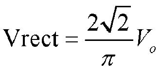

- A valid value Irect of a fundamental component of the current is:

- Therefore, converted input resistance R of the full-bridge rectifier of the power transmitting terminal device is:

- A voltage gain of the wireless charging system is obtained by combining the foregoing equations:

- Voltage gain modulus length:

- Current gain:

- Current gain modulus length:

- It can be learned from the expressions that the voltage gain Mv and the current gain Mi are six-variable functions. To be specific, the voltage gain Mv and the current gain Mi are both related to the coupling factor k, the turns ratio n, the resonant capacitance ratio α, the modulation capacitance ratio β, a load magnitude (the quality factor Qn represents the load magnitude of the wireless charging system), and the operating angular frequency ωn.
- Based on the equivalent circuit shown in
FIG. 9 , a voltage gain curve shown inFIG. 10 is drawn with the coil turns ratio n = 1, the coil coupling factor k = 0.5, and the resonant capacitance ratio α = 25/21, where a horizontal axis is the scalarized operating angular frequency ωn, and a vertical axis is the voltage gain Mv. When k = 0.5, according to the wireless charging Qi standard, the operating frequency is 100 kHz to 200 kHz, and the scalarized operating angular frequency ωn is 1.0 to 2.0. UsingFIG. 10 as an example, when Qn = 0.1, and con = 1.6, and β = 0.12, Mv ≈ 0.9; when β = 0.015, Mv ≈ 0.68, that is, Mv increases with the increase of β, and the voltage gain Mv is positively correlated with the modulation capacitance ratio β. UsingFIG. 10 as an example, when β = 0.015, and ωn = 1.6, and Qn = 0.1, Mv ≈ 0.68; when Qn = 0.5, Mv ≈ 0.6, that is, Mv decreases with the increase of Qn, and the voltage gain Mv is negatively correlated with the quality factor Qn. In addition, with reference to principles of ASK modulation described inFIG. 3 to FIG. 6 , it can be learned that the voltage gain is increased when the modulation capacitor is connected, and the voltage gain is decreased when the modulation capacitor is disconnected. Therefore, if the voltage gain is larger after the modulation capacitor is connected, a voltage difference of Vrect is larger after the modulation capacitor is disconnected. Therefore, increasing the modulation capacitance ratio β (that is, increasing the modulation capacitance) helps increase a voltage difference in ASK modulation, that is, helps increase the voltage difference of Vrect. For example, when Qn = 0.1, and con = 1.6, and β = 0.015, if con = 1.6, the voltage gain Mv ≈ 0.68. In this case, if the voltage difference δV of Vrect is 98 mV, as described above, 98 mV < 100 mV, and ASK communication failure may occur. If con = 1.6 and β = 0.12, the voltage gain Mv ≈ 0.9. In this case, the voltage difference δV of Vrect is 98 mV * (0.9/0.68) ≈ 130 mV, and 130 mV > 100 mV, which satisfies an ASK communication requirement, and δV is increased from 98 mV to 130 mV when the modulation capacitance ratio β is increased. Apparently, increasing the modulation capacitance ratio β can avoid impact of an excessively small voltage difference of Vrect on ASK communication quality, and decreasing the modulation capacitance ratio β can avoid impact of an excessively large voltage difference of Vrect on ASK communication quality. - With reference to
FIG. 11 , a voltage gain curve is drawn with the quality factor Qn = 1.0 and the relatively low coupling factor k = 0.1, where a horizontal axis is the scalarized operating angular frequency con, and a vertical axis is the voltage gain Mv. The modulation capacitance ratio β is 0.1, 0.25, 0.5, 0.75, and 1.0 in sequence. When k = 0.1, according to the wireless charging Qi standard, the operating frequency is 100 kHz to 200 kHz, and the scalarized operating angular frequency ωn is 1.35 to 2.7. Because a value of k = 0.1 is relatively small, the leakage inductance L1s becomes large, and the frequency needs to be reduced (that is, the operating angular frequency is reduced) to improve a loading capability. Therefore, the system works near ωn = 1.35 (as shown inFIG. 11 , ωn is 1.05 to 1.45). For example, when con = 1.3 and β = 0.75, MV ≈ 0.33; when con = 1.3 and β = 0.1, MV ≈ 0.2, that is, Mv increases with the increase of β. Apparently, increasing the modulation capacitance ratio β can increase a loop voltage gain, thereby improving the loading capability and enhancing ASK communication quality. With reference toFIG. 12 , a voltage gain curve is drawn with the quality factor Qn = 1.0 and the relatively high coupling factor k = 0.8, where a horizontal axis is the scalarized operating angular frequency con, and a vertical axis is the voltage gain Mv. The modulation capacitance ratio β is 0.1, 0.25, 0.5, 0.75, and 1.0 in sequence. In comparison withFIG. 10 , inFIG. 12 , the coupling factor k (k = 0.8) is relatively large, the leakage inductance L1s becomes small, and therefore the referenceangular frequency 
FIG. 12 , before ωn = 1.05, Mv decreases with the increase of β, and negative ASK modulation occurs. Therefore, in the positive ASK modulation process (the scalarized operating angular frequency is 1.05 to 1.26), increasing the modulation capacitance ratio β can increase the loop voltage gain, thereby improving the loading capability and enhancing ASK communication quality. - When the wireless charging system is lightly loaded, for example, fully charged, or a current output by the wireless charging system in a stage in which the electronic device has just established communication (negotiated charging power) is relatively small, assuming that the modulation capacitance ratio β is 0.015 and 0.12 respectively, a voltage gain curve is shown in
FIG. 13 , where a horizontal axis is the scalarized operating angular frequency ωn, and a vertical axis is the voltage gain Mv. With reference to the previous analysis, Vrect needs to have a valid voltage difference during ASK communication. InFIG. 13 , there is a turning point (minimum value con = 1.3) for the voltage gain. A magnitude of the turning point depends on the coupling factor k. When the modulation capacitance is relatively large (β = 0.12), the voltage gain is relatively large (Mv > 0.8), and the capacitor C3 is charged during communication, but when the modulation capacitor is disconnected, the voltage gain needs to be reduced to achieve a valid voltage difference of Vrect. However, in a light load state, the load is insufficient, and this causes the voltage of the capacitor C3 to increase continuously, resulting in a distortion of a communication waveform. - When the wireless charging system is fully loaded, assuming that the modulation capacitance ratio β is 0.015 and 0.12 respectively, a voltage gain curve is shown in
FIG. 14 , where a horizontal axis is the scalarized operating angular frequency con, and a vertical axis is the voltage gain Mv. When the wireless charging system is fully loaded, increasing the load reduces the voltage difference of the rectified voltage Vrect during communication, and due to the increase of the load, the operating angular frequency ωn decreases, and this further reduces the voltage difference of the rectified voltage Vrect, resulting in demodulation failure on the transmitting terminal. For example, when ωn = 1.6 and β = 0.12, Mv ≈ 0.62; when β = 0.015, Mv ≈ 0.52, where a voltage gain difference is 0.1. When con decreases to 1.2 and β = 0.12, Mv ≈ 0.8; when β = 0.015, Mv ≈ 0.75, where a voltage gain difference is 0.05. Apparently, after the operating angular frequency ωn decreases, the voltage gain difference decreases, resulting in decrease of the voltage difference of the rectified voltage Vrect. However, as shown inFIG. 14 , increasing the modulation capacitance ratio β (that is, increasing the modulation capacitance) helps increase the voltage gain Mv, thereby increasing the voltage difference of the rectified voltage Vrect. - Using the coil turns ratio n = 1, the modulation capacitance ratio β = 0.12, and the quality factor Qn = 1.0 as an example, a voltage gain curve shown in
FIG. 15 is drawn, where a horizontal axis is the scalarized operating angular frequency ωn, and a vertical axis is the voltage gain Mv. The voltage gain Mv is negatively correlated with the coupling factor k and negatively correlated with the resonant capacitance ratio α. When the coupling factor is relatively large, the leakage inductance L1s is relatively small, and the resonant capacitor is overcompensated. In this case, the capacitance value of the resonant capacitor is relatively large, and the resonant capacitance ratio α is relatively small. In this case, when the modulation capacitor is connected, the voltage gain decreases, and when the modulation capacitor is disconnected, the voltage gain increases, resulting in negative ASK modulation. Specifically, with reference toFIG. 16 , when the coupling factor k (k = 0.8) is relatively large, the leakage inductance L1s becomes small, and therefore the referenceangular frequency 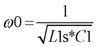
FIG. 16 , there is an intersection point between the two curves of β = 0.015 and β = 0.095 (when α = 0.25, the intersection point is at wn = 0.8; when α = 0.5, the intersection point is at wn = 0.85; when α = 1.0, the intersection point is at wn = 1.0). Before the intersection point, because Mv decreases with the increase of (3, negative ASK modulation occurs. In actual operation, the coil coupling factor k is related to a charging position of the electronic device. Therefore, when the coupling factor k is relatively low, generally the charging position is relatively biased. When the coupling factor k is relatively high, generally an air gap between coils is insufficient or the charging position is in the middle. Therefore, ASK communication quality is mainly affected by negative ASK modulation caused when the coupling factor is relatively large. - With reference to
FIG. 17 , a voltage gain curve is drawn with the quality factor Qn = 1.0 and the relatively high coupling factor k = 0.8, where a horizontal axis is the operating angular frequency ωn, and a vertical axis is the voltage gain Mv. The resonant capacitance ratio α is 0.25, 0.33, 0.5, 1.0, and 5 in sequence. In the wireless charging Qi standard, the operating frequency is 100 kHz to 200 kHz. When the coupling factor is 0.8, the scalarized operating angular frequency ωn of the system is below 1.26. For example, when con = 0.9 and α = 1.0, Mv ≈ 1.05; when con = 0.9 and α = 0.25, Mv ≈ 1.07, that is, Mv decreases with the increase of α. Apparently, decreasing the resonant capacitance ratio α can increase the voltage gain, thereby improving the loading capability and enhancing ASK communication quality. In summary, reasons that affect ASK communication quality and cause relatively poor compatibility of the electronic device are mainly as follows: negative ASK modulation, the communication waveform distortion when the wireless charging system is lightly loaded, and decrease (generally, the voltage difference of the rectified voltage Vrect is decreased more apparently when the wireless charging system is fully loaded) or increase of the voltage difference of the rectified voltage Vrect of the wireless charging system. Based on the foregoing analysis, the solutions provided in embodiments of this application mainly resolve the foregoing problems according to the following principles: The problem of negative ASK modulation can be resolved by optimizing the resonant capacitor C2 or the modulation capacitor of the power receiving terminal electronic device; the problem of the communication waveform distortion when the wireless charging system is lightly loaded can be resolved by optimizing the impedance of the power receiving terminal electronic device; and the problem of decrease or increase of the voltage difference of the rectified voltage Vrect can be resolved by optimizing the equivalent capacitive reactance (for example, the modulation capacitance or the resonant capacitance) of the power receiving terminal electronic device. - Based on the foregoing analysis result, an electronic device provided in an embodiment of this application is described in detail as follows:
In an example 1, an embodiment of this application provides an electronic device. As shown inFIG. 18 , the electronic device includes adevice circuit 50, avoltage conversion circuit 203, arectifier circuit 202, aresonant circuit 201, and amodulation circuit 204. An input end of thedevice circuit 50 is coupled to an output end of thevoltage conversion circuit 203, an input end of thevoltage conversion circuit 203 is coupled to an output end of therectifier circuit 202, an input end of therectifier circuit 202 is coupled to an output end of theresonant circuit 201, and themodulation circuit 204 is coupled to the input end of therectifier circuit 202. Theresonant circuit 201 is configured to induce an alternating magnetic field sent by a power transmitting terminal device to generate an induced alternating current; themodulation circuit 204 is configured to modulate an amplitude of the alternating current; therectifier circuit 202 is configured to rectify the amplitude-modulated induced alternating current to generate a rectified voltage Vrect; and thevoltage conversion circuit 203 is configured to convert the rectified voltage into a load voltage and output the load voltage to thedevice circuit 50. - The
resonant circuit 201 includes a resonant inductor L2 and a resonant capacitor control circuit ci1 connected in series to the resonant inductor L2. A first end of the resonant inductor L2 is coupled to therectifier circuit 202, a second end of the resonant inductor L2 is coupled to a first end a of the resonant capacitor control circuit ci1, and a second end of the resonant capacitor control circuit ci1 is coupled to therectifier circuit 202. The resonant capacitor control circuit ci1 is configured to adjust a capacitance value of a resonant capacitor connected to the resonant circuit. In this example, the resonant capacitor control circuit ci1 can adjust the capacitance value of the resonant capacitor connected to the resonant circuit. Therefore, with reference to the analysis ofFIG. 15 ,FIG. 16 , andFIG. 17 , by adjusting the capacitance value of the resonant capacitor, a resonant capacitance ratio α can be adjusted. Because a gain of the rectified voltage can be indirectly adjusted by adjusting the resonant capacitance ratio a, a problem of negative ASK modulation or decrease or increase of a voltage difference of the rectified voltage Vrect is resolved. Therefore, ASK communication quality is improved, and compatibility of the electronic device in wireless charging is improved. - The resonant capacitor
control circuit ci 1 includes a capacitance value switching network formed by at least one switch and at least one capacitor, and the resonant capacitor control circuit ci1 is configured to control a status of the switch to adjust the capacitance value of the resonant capacitor connected to the resonant circuit. - Specifically, as shown in
FIG. 19 , the resonant capacitor control circuit ci1 includes an adjustable capacitor Cj, a first end of the adjustable capacitor Cj is coupled to the second end of the resonant inductor L2, and a second end of the adjustable capacitor Cj is coupled to therectifier circuit 202. In this way, the capacitance value of the resonant capacitor connected to the resonant circuit can be adjusted by directly adjusting a capacitance value of the adjustable capacitor Cj. - As shown in
FIG. 20 , the resonant capacitor control circuit ci1 includes at least two parallel resonant capacitor regulating branches F (F1 to Fn). A first end of the resonant capacitor regulating branch F1 (F2 to Fn) is coupled to the second end (node a) of the resonant inductor L2, and a second end of the resonant capacitor regulating branch F1 (F2 to Fn) is coupled to the rectifier circuit 202 (node b). A first switch Ka and a first capacitor Ca are connected in series on at least one resonant capacitor regulating branch F1 (F2 to Fn), and the resonant capacitor control circuit ci1 adjusts, by adjusting a status of a first switch Ka on the at least one resonant capacitor regulating branch F1 (F2 to Fn), the capacitance value of the resonant capacitor connected to theresonant circuit 201. For example, currently, the first switch Ka of the resonant capacitor regulating branch F1 is controlled to be in an on state by default. In this case, the first capacitor Ca on the resonant capacitor regulating branch F1 is used as the resonant capacitor, and the resonant capacitor and the resonant inductor L2 form the resonant circuit to receive power sent by a power transmitting terminal electronic device. When a voltage gain needs to be increased, the first switch Ka of the resonant capacitor regulating branch F2 may be controlled to be in an on state. In this case, a capacitor equivalent to the first capacitor Ca on the resonant capacitor regulating branch F1 and the first capacitor Ca on the resonant capacitor regulating branch F2 that are connected in parallel is used as the resonant capacitor, and the resonant capacitor and the resonant inductor L2 form the resonant circuit to receive power sent by the power transmitting terminal electronic device. Because the capacitance value of the resonant capacitor becomes large, the resonant capacitance ratio is reduced, and the voltage gain is increased. Certainly, first switches Ka of more resonant capacitor regulating branches may alternatively be controlled to be turned on if the voltage gain obtained by connecting two first capacitors in parallel is still insufficient. As shown inFIG. 21 , one resonant capacitor regulating branch F1 (F2 to Fn) includes a second capacitor Cb, a first end of the second capacitor Cb is coupled to the second end of the resonant inductor L2, and a second end of the second capacitor Cb is coupled to therectifier circuit 202. A control principle of the second capacitor Cb is the same as the control of any resonant capacitor regulating branch shown inFIG. 21 . In an initial state, the second capacitor Cb is used as the resonant capacitor, and the resonant capacitor and the resonant inductor L2 form the resonant circuit to receive power sent by the power transmitting terminal electronic device. When the voltage gain needs to be increased, the first switch Ka of the resonant capacitor regulating branch F1 may be controlled to be in the on state. In this case, a capacitor equivalent to the second capacitor Cb and the first capacitor Ca on the resonant capacitor regulating branch F1 that are connected in parallel is used as the resonant capacitor, and the resonant capacitor and the resonant inductor L2 form the resonant circuit to receive power sent by the power transmitting terminal electronic device. Because the capacitance value of the resonant capacitor becomes large, the resonant capacitance ratio is reduced, and the voltage gain becomes large. - For example, the first switch Ka may be a bidirectional switch, and a current flowing in the
resonant circuit 201 is in a form of an alternating current. Therefore, the current needs to be conducted from a to b or from b to a. Therefore, the first switch needs to have a bidirectional conduction function. Specifically, the bidirectional switch may be a reverse series switching transistor. Because the switching transistor generally has a unidirectional conduction characteristic, a bidirectional conduction effect needs to be achieved by using two reverse series switching transistors. Specifically, in some embodiments of this application, the switching transistor has a gate (gate, g) and a first electrode, for example, a drain (drain, d), and a second electrode, for example, a source (source, s). In this embodiment of this application, the switching transistor may be an N-type switching transistor or a P-type switching transistor. UsingFIG. 22 as an example, the first switch K1 includes a switching transistor Qs1 and a switching transistor Qs2. Using the N-type switching transistor as an example, a drain (drain, d) of Qs1 is connected to a drain d of Qs2, a source (source, s) of Qs1 is connected to the node a through the first capacitor Ca, and a source s of Qs2 is connected to the node b. Gates (gate, g) of Qs1 and Qs2, as gating ends of the first switch 31, are configured to receive gating signals. In some embodiments of this application, the electronic device may include agating control circuit 207 and adrive circuit 206 shown inFIG. 22 , where thegating control circuit 207 is configured to generate a logic signal, and thedrive circuit 206 may convert the logic signal into a voltage signal and provide the voltage signal as a gating signal to the gates g of Qs1 and Qs2 to control turn-on or turn-off of Qs1 and Qs2. When the N-type switching transistor is turned on, a direction of a current is from d to s (an anode (anode, a) of a parasitic diode D1 is coupled to the source s of Qs1, a cathode (cathode, c) of the parasitic diode D1 is coupled to the drain d of Qs1, and a parasitic diode D2 in Qs2 is connected in the same way as the parasitic diode D1 in Qs1). Using Qs1 as an example, a conduction direction of the parasitic capacitor D1 in a freewheeling function is from s to d. Therefore, if the first switch K includes one switching transistor, a current in the direction from s to d cannot be cut off when the switching transistor is in an off state. In this solution, when Qs1 and Qs2 are turned on at the same time, a current from the node a to the node b can pass through the parasitic diode of Qs1 and the drain d and source s of Qs2 in sequence; and a current from the node b to the node a can pass through the parasitic diode of Qs2 and the drain d and source s of Qs1 in sequence. - Because the resonant capacitor is connected in series in the resonant circuit, during power transmission, main power is transmitted by using the resonant capacitor. Therefore, adjusting the resonant capacitor causes system instability. Therefore, capacitive reactance of ASK modulation is usually not optimized by adjusting the resonant capacitor. However, when negative ASK modulation occurs, ASK communication fails directly. Therefore, in this application, the resonant capacitor is mainly adjusted during negative ASK modulation. With reference to the foregoing analysis of
FIG. 16 , a main cause of negative ASK modulation is that the resonant capacitor is overcompensated. When negative ASK modulation of the rectified voltage Vrect occurs, the resonant capacitor control circuit ci1 is configured to increase the capacitance value of the resonant capacitor connected to the resonant circuit, to recover positive ASK modulation of the rectified voltage. Specific reasons are analyzed as follows: With reference toFIG. 16 , the coupling factor k becomes large, the leakage inductance L1s becomes small, and therefore the referenceangular frequency 
angular frequency 
- As shown in
FIG. 23 , a waveform graph of Vrect when the electronic device is in positive ASK modulation is shown by awaveform graph 1, and a waveform graph when the electronic device is in negative ASK modulation is shown by a stage T1 in awaveform graph 2, where a phase difference between the waveform graph of Vrect during negative ASK modulation and the waveform graph of Vrect during negative ASK modulation is 180°. In this case, thedevice circuit 50 can detect the rectified voltage Vrect. When negative modulation of the rectified voltage occurs, the resonant capacitor control circuit cil increases the capacitance value of the resonant capacitor connected to theresonant circuit 201, to recover positive modulation of the rectified voltage. - For example, with reference to
FIG. 19 , when negative ASK modulation occurs, the capacitance value of the adjustable capacitor Cj may be increased, so that the resonant capacitance ratio α is reduced and that negative ASK modulation is corrected to positive ASK modulation. For another example, with reference toFIG. 20 , currently, the first switch Ka of the resonant capacitor regulating branch F1 is controlled to be in the on state by default. In this case, the first capacitor Ca on the resonant capacitor regulating branch F1 is used as the resonant capacitor, and the resonant capacitor and the resonant inductor L2 form the resonant circuit to receive power sent by the power transmitting terminal electronic device. When the voltage gain needs to be increased, the first switch Ka of the resonant capacitor regulating branch F2 may be controlled to be in the on state. In this case, the capacitor equivalent to the first capacitor Ca on the resonant capacitor regulating branch F1 and the first capacitor Ca on the resonant capacitor regulating branch F2 that are connected in parallel is used as the resonant capacitor, and the resonant capacitor and the resonant inductor L2 form the resonant circuit to receive power sent by the power transmitting terminal electronic device. - Because the capacitance value of the resonant capacitor becomes large, the resonant capacitance ratio α is reduced, and negative ASK modulation is corrected to positive ASK modulation. Certainly, first switches Ka of more resonant capacitor regulating branches may alternatively be controlled to be turned on if two first capacitors connected in parallel are insufficient for correcting negative ASK modulation to positive ASK modulation. With reference to
FIG. 23 , a sequence of the gating signals of Qs1 and Qs2 is also provided. When negative modulation of the rectified voltage occurs in the stage T1, an objective of increasing the capacitance value of the resonant capacitor is achieved by inputting the gating signals of the sequence at the gates g of Qs1 and Qs2 of one or more resonant capacitor regulating branches. - In an example 2, as shown in
FIG. 24 , an electronic device is provided and includes adevice circuit 50, avoltage conversion circuit 203, arectifier circuit 202, aresonant circuit 201, and amodulation circuit 204. An input end of thedevice circuit 50 is coupled to an output end of thevoltage conversion circuit 203, an input end of thevoltage conversion circuit 203 is coupled to an output end of therectifier circuit 202, an input end of therectifier circuit 202 is coupled to an output end of theresonant circuit 201, and themodulation circuit 204 is coupled to the input end of therectifier circuit 202. Theresonant circuit 201 is configured to induce an alternating magnetic field sent by a power transmitting terminal device to generate an induced alternating current; themodulation circuit 204 is configured to modulate an amplitude of the alternating current; the rectifier circuit is configured to rectify the amplitude-modulated induced alternating current to generate a rectified voltage; and thevoltage conversion circuit 203 is configured to convert the rectified voltage into a load voltage and output the load voltage to thedevice circuit 50. The electronic device further includes a load control circuit 208. The load control circuit 208 is coupled to the input end of therectifier circuit 202, and the load control circuit 208 is configured to connect a resistance value to the input end of therectifier circuit 202 when the rectified voltage is at a low level. - In this example, because the load control circuit is coupled to the input end of the rectifier circuit, the
load control circuit 2 can connect the resistance value to the input end of the rectifier circuit when the rectified voltage is at the low level. Based on the analysis ofFIG. 13 , a modulation capacitor is disconnected when the rectified voltage is at the low level. In this case, a voltage gain needs to be reduced. Because the resistance value is connected to the input end of the rectifier circuit, energy of the input end of the rectifier circuit can be forcibly released when the modulation capacitor is disconnected. In this way, continuous increase of a voltage of a capacitor C3 is avoided, and a modulation waveform is improved by dividing the rectified voltage. For example, low level burrs or oscillations are eliminated. The load control circuit 208 includes a resistance value switching network formed by at least one switch and at least one resistor, and the load control circuit 208 is configured to control a status of the switch to adjust the resistance value connected to the input end of the rectifier circuit. - In addition, the
device circuit 50 is further configured to detect power Pout corresponding to the rectified voltage Vrect and power Pri consumed by the resistance value connected by the load control circuit 208 to the input end of the rectifier circuit; and the load control circuit 208 is configured to disconnect the resistance value when it is determined that the power Pout corresponding to the rectified voltage is greater than the power Pri consumed by the resistance value. - Because the solution provided in this embodiment of this application is based on a differential biphase coding scheme in which the
rectifier circuit 202 includes two input ends AC1 and AC2 as shown inFIG. 4 , in this embodiment of this application, two load control circuits 208 (208-1 and 208-2) are included, as shown inFIG. 24 , where the load control circuit 208-1 is connected to theinput end AC 1 of therectifier circuit 202 and the load control circuit 208-2 is connected to the input end AC2 of therectifier circuit 202. Structures of the load control circuits connected to the two input ends AC1 and AC2 are the same. As shown inFIG. 25 , a schematic diagram of a load control circuit 208 is provided. The load control circuit 208 includes a first switch Ka and a first resistor R1, a first end of the first resistor R1 is coupled to the input end AC 1 (or AC2) of therectifier circuit 202, a second end of the first resistor R1 is coupled to a first end of the first switch Ka, and a second end of the first switch Ka is grounded GND. - As shown in
FIG. 26a , the first switch Ka includes a switching transistor Q1-2. As described above, the switching transistor Q1-2 may include an N-type switching transistor or a P-type switching transistor. It can be learned from the foregoing description that when the N-type switching transistor is turned on, a direction of a current is from a drain d to a source s, and the current needs to be released to the GND through a resistor. Therefore, when the N-type switching transistor is used, the source s of the switching transistor can be directly grounded, so that floating of the source of the switching transistor is avoided. For example, the source s of the switching transistor is grounded GND. In this way, when the N-type switching transistor is used, the source s has a fixed value, and the N-type switching transistor can be turned on as long as a voltage of a gate g is higher than a voltage of the source s. The circuit design is relatively simple. When other manners are used, for example, when the P-type switching transistor is used, when the P-type switching transistor is turned on, a direction of a current is from a source s to a drain d, and the current needs to be released to the GND through a resistor. Therefore, the drain d is grounded GND. However, a voltage of the source s is not fixed, and a voltage of a gate g that controls turn-on of the P-type switching transistor cannot be determined. This is because a ground voltage of the source s has two states. When the P-type switching transistor is turned off, the voltage is at a low level, and when the P-type switching transistor is turned on, the voltage is close to that of AC1. Therefore, when the first switch Ka is the P-type switching transistor, an isolated power control or bootstrap boost circuit needs to be separately designed to provide a gating signal for the P-type switching transistor. The load control circuit 208-1 connected to AC1 is described above.FIG. 26b also shows that a first switch K in the load control circuit 208-2 connected to AC2 may include a switching transistor Q2-2 whose connection mode is similar to that of the switching transistor Q1-2 and is not described. - As shown in
FIG. 27 , a sequence diagram of a gating signal of Q1-2 (Q2-2) is provided. For example, in an establishment stage of power transmission of the electronic device, when the electronic device is in a light load state, when Vrect is at the low level, the first switch Ka of the load control circuit 208 is turned on (when the switching transistor Q1-2 (Q2-2) is used, the switching transistor Q1-2 (Q2-2) is controlled to be turned on by using a gating signal), and the first resistor is connected to the input end AC1 (AC2) of therectifier circuit 202. In this case, after ASK communication is completed, thedevice circuit 50 detects power Pout (Vout * Iout, where Vout is an output voltage of an LDO, and Iout is an output current of the LDO) corresponding to the rectified voltage Vrect and power Pri consumed by the first resistor connected by the load control circuit 208 to the input end of the rectifier circuit. As shown inFIG. 27 , when it is detected that Pout is greater than Pri after a time T2, the first switch Ka is turned off (when the switching transistor Q1-2 (Q2-2) is used, the switching transistor Q1-2 (Q2-2) is controlled to be turned off by using a gating signal. For details about controlling the status of the switching transistor by using the gating signal, refer to the description in the example 1. Details are not described herein again). - In an example 3, as shown in
FIG. 28 , an electronic device is provided and includes adevice circuit 50, avoltage conversion circuit 203, arectifier circuit 202, aresonant circuit 201, and amodulation circuit 204. An input end of thedevice circuit 50 is coupled to an output end of thevoltage conversion circuit 203, an input end of thevoltage conversion circuit 203 is coupled to an output end of therectifier circuit 202, an input end of therectifier circuit 202 is coupled to an output end of theresonant circuit 201, and themodulation circuit 204 is coupled to the input end of therectifier circuit 202. Theresonant circuit 201 is configured to induce an alternating magnetic field sent by a power transmitting terminal device to generate an induced alternating current; themodulation circuit 204 is configured to modulate an amplitude of the alternating current; therectifier circuit 202 is configured to rectify the amplitude-modulated induced alternating current to generate a rectified voltage Vrect; and the voltage conversion circuit is configured to convert the rectified voltage into a load voltage and output the load voltage to thedevice circuit 50. - The
modulation circuit 204 is configured to adjust a capacitance value of a modulation capacitor connected to the input end of therectifier circuit 202. - Because the solution provided in this embodiment of this application is based on a differential biphase coding scheme in which the
rectifier circuit 202 includes two input ends AC1 and AC2 as shown inFIG. 4 , in this embodiment of this application, two modulation circuits 204 (204-1 and 204-2) are included, as shown inFIG. 28 , where the modulation circuit 204-1 is connected to the input end AC1 of therectifier circuit 202 and the modulation circuit 204-2 is connected to the input end AC2 of therectifier circuit 202. Structures of the modulation circuits connected to the two input ends AC1 and AC2 are the same. Certainly, the two modulation circuits 204-1 and 204-2 may be integrated into one modulation circuit, as shown inFIG. 4 . - With the analysis of
FIG. 10 ,FIG. 11 ,FIG. 12 ,FIG. 13, and FIG. 14 , because the modulation circuit can adjust the capacitance value of the modulation capacitor connected to the input end of the rectifier circuit, a value of a modulation capacitance ratio can be adjusted. Because a gain of the rectified voltage can be indirectly adjusted by adjusting the value of the modulation capacitance ratio, a problem of negative ASK modulation or decrease or increase of a voltage difference of the rectified voltage Vrect is resolved. Therefore, ASK communication quality is improved, and compatibility of the electronic device in wireless charging is improved. - The modulation circuit includes a capacitance value switching network formed by at least one switch and at least one capacitor, and the modulation circuit is configured to control a status of the switch to adjust the capacitance value of the modulation capacitor connected to the input end of the rectifier circuit.
- Specifically, as shown in
FIG. 29 , themodulation circuit 204 includes a first switch Ka and an adjustable capacitor Cj, a first end of the adjustable capacitor Cj is coupled to the input end AC1 (AC2) of therectifier circuit 202, a second end of the adjustable capacitor Ci is coupled to a first end of the first switch Ka, and a second end of the first switch Ka is coupled to the ground GND. The first switch Ka may be a switching transistor Q1 -1, such as an N-type switching transistor or a P-type switching transistor. As shown inFIG. 30 , because the second end of the first switch Ka is coupled to the ground GND, the N-type switching transistor may be preferably used as the first switch Ka, as described above. - For example, as shown in
FIG. 31 , themodulation circuit 204 includes a first switch Ka and at least two parallel modulation capacitor branches Y (Y1 to Yn), a first end of the modulation capacitor branch Y (Y1 to Yn) is coupled to the input end AC1 of therectifier circuit 202, a second end of the modulation capacitor branch Y (Y1 to Yn) is coupled to a first end of the first switch Ka, and a second end of the first switch Ka is coupled to the ground GND. Any modulation capacitor branch Y (Y1 to Yn) includes a first capacitor Ca and a second switch Kb, a first end of the second switch Kb is coupled to the input end of therectifier circuit 202, a second end of the second switch Kb is coupled to a first end of the first capacitor Ca, and a second end of the first capacitor Ca is coupled to the first end of the first switch Ka. Themodulation circuit 204 adjusts, by adjusting a status of the second switch Kb on the at least one modulation capacitor branch Y (Y1 to Yn), the capacitance value of the modulation capacitor connected to the input end of therectifier circuit 204. For example, currently, the second switch Kb of the modulation capacitor branch Y1 is controlled to be in an on state by default, and a voltage gain needs to be increased. In this case, the second switch Kb of the modulation capacitor branch Y2 is controlled to be in an on state. In this case, when the first switch Ka is turned on, the modulation capacitor connected to the input end AC1 (AC2) of therectifier circuit 202 is a capacitor equivalent to the first capacitor Ca on the modulation capacitor branch Y1 and the first capacitor Ca on Y2 that are connected in parallel. If the voltage gain needs to be increased, the second switch Kb of the modulation capacitor branch Y3 continues to be controlled to be in an on state. In this way, the modulation capacitor connected to the input end AC1 (AC2) of therectifier circuit 202 is a resistor equivalent to three first capacitors Ca on the modulation capacitor branches Y1, Y2, and Y3 that are connected in parallel, thereby increasing the capacitance value of the modulation capacitor connected to the input end of therectifier circuit 204. If the voltage gain needs to be decreased, the second switch Kb of the modulation capacitor branch Y3 can be controlled to be in an off state, to reduce the capacitance value of the modulation capacitor connected to the input end of therectifier circuit 204. Certainly, the foregoing is merely an example, and it is also possible to select to control two or more modulation capacitor branches Y at the same time based on an actual situation. This is not specifically limited in this application. In addition, as shown inFIG. 31 , a second capacitor Cb is connected in series on any modulation capacitor branch Y In this way, Cb is equivalent to Cm1 (Cm2) inFIG. 5 . A control principle of the second capacitor Cb is the same as the control of any modulation capacitor branch Y shown inFIG. 31 . In an initial state, the second capacitor Cb is used as the modulation capacitor to connect to the input end AC1 (AC2) of therectifier circuit 202. When the voltage gain needs to be increased, the second switch Kb on any modulation capacitor branch Y is controlled to be turned on. When the voltage gain needs to be reduced, the second switch Kb currently in the on state on any modulation capacitor branch Y is controlled to be turned off. In the example 3, as shown inFIG. 32a , the second switch Kb in the modulation circuit 204-1 may be a switching transistor Q1-1, where a first capacitor Ca (Ca1) and a first switch Ka (Ka1) are also shown inFIG. 32a . As shown inFIG. 32b , the second switch Kb in the modulation circuit 204-2 may be a switching transistor Q2-1, where a first capacitor Ca (Ca2) and a first switch Ka (Ka2) are also shown inFIG. 32b . The switching transistor Q1-1 and the switching transistor Q2-1 may be N-type switching transistors or P-type switching transistors. For details about controlling a status of a switching transistor by using a gating signal, refer to the description in the example 1. Details are not described herein again. - As described in the foregoing example 1, because the resonant capacitor is connected in series in the resonant circuit, during power transmission, main power is transmitted by using the resonant capacitor. Therefore, adjusting the resonant capacitor causes system instability. Therefore, capacitive reactance of ASK modulation is usually not optimized by adjusting the resonant capacitor. However, when negative ASK modulation occurs, ASK communication fails directly. Therefore, in this application, the resonant capacitor is mainly adjusted during negative ASK modulation. With reference to the analysis of
FIG. 15 , a main cause of negative ASK modulation is that the resonant capacitor is overcompensated. Although adjusting the resonant capacitor can also optimize the voltage difference of Vrect, considering impact of the adjustment on system stability, the voltage difference of the rectified voltage Vrect is mainly optimized by adjusting the modulation capacitor in this embodiment of this application. - For example, when the voltage difference of the rectified voltage Vrect is relatively small due to abnormal ASK modulation when the electronic device is in a full load or heavy load state, or the voltage difference of the rectified voltage Vrect is excessively large and affects communication quality, the voltage difference of the rectified voltage Vrect can be restored to a normal range by adjusting the modulation capacitor. The
device circuit 50 is further configured to detect the rectified voltage; and when a maximum voltage difference δVrect of the rectified voltage is less than or equal to a first threshold voltage Vset-th1 and the rectified voltage is at the low level, themodulation circuit 204 is configured to increase the capacitance value of the modulation capacitor connected to the input end of the rectifier circuit; or when a maximum voltage difference of the rectified voltage is greater than or equal to a second threshold voltage Vset-th2 and the rectified voltage is at the low level, the modulation circuit is configured to reduce the capacitance value of the modulation capacitor connected to the input end of the rectifier circuit, where Vset-th2 is greater than Vset-th1. With reference to the description ofFIG. 5 , when the modulation capacitor is connected to the rectifier circuit, an amplitude of Vrect is increased, that is, corresponding to the high level of the modulation waveform inFIG. 5 . When the modulation capacitor is disconnected from the rectifier circuit, the amplitude of Vrect is reduced, that is, corresponding to the low level of the modulation waveform inFIG. 5 . Therefore, by referring to the Qi specification, the vset-th1 can determine a smallest value of δVrect that does not affect ASK communication quality. When the maximum voltage difference δVrect is less than or equal to the first threshold voltage Vset-th1, and the rectified voltage is at the low level, the capacitance value of the modulation capacitor connected to the input end of the rectifier circuit is increased. By referring to the Q profile, the Vset-th2 can determine a largest value of δVrect that does not affect ASK communication quality. When the maximum voltage difference δVrect is greater than or equal to the Vset-th2, and the rectified voltage is at the low level, the capacitance value of the modulation capacitor connected to the input end of the rectifier circuit is increased. Because the capacitance value of the modulation capacitor is increased, when the modulation waveform is at the high level, the amplitude of Vrect is higher, so that δVrect is increased. Conversely, if the capacitance value of the modulation capacitor is decreased, when the modulation waveform is at the high level, the amplitude of Vrect is reduced, so that δVrect is decreased. - For example, with reference to
FIG. 29 andFIG. 30 , when δVrect ≤ Vset-th1, the capacitance value of the adjustable capacitor Cj can be increased, and when δVrect ≥ Vset-th2, the capacitance value of the adjustable capacitor Cj can be decreased. With reference toFIG. 31 , currently, the second switch Kb of the modulation capacitor branch Y1 is controlled to be in the on state by default. When δVrect ≤ Vset-th1, the second switch Kb of the modulation capacitor branch Y2 is controlled to be in the on state. In this case, when the first switch Ka is turned on, the modulation capacitor connected to the input end AC1 (AC2) of therectifier circuit 202 is a capacitor equivalent to the first capacitor Ca on the modulation capacitor branch Y1 and the first capacitor Ca on Y2 that are connected in parallel. If δVrect ≤ Vset-th1, the second switch Kb of the modulation capacitor branch Y3 continues to be controlled to be in the on state. In this way, the modulation capacitor connected to the input end AC1 (AC2) of therectifier circuit 202 is a resistor equivalent to three first capacitors Ca on the modulation capacitor branches Y1, Y2, and Y3 that are connected in parallel, thereby increasing the capacitance value of the modulation capacitor connected to the input end of therectifier circuit 204. If δVrect ≥ Vset-th2, the second switch Kb of the modulation capacitor branch Y3 can be controlled to be in the off state, to reduce the capacitance value of the modulation capacitor connected to the input end of therectifier circuit 204. Certainly, the foregoing is merely an example, and it is also possible to select to control two or more modulation capacitor branches Y at the same time based on an actual value of δVrect. This is not specifically limited in this application. As shown inFIG. 33 , a waveform graph of a gating signal when Q1-1 (Q2-1) is an N-type switching transistor is also provided. When δVrect ≤ Vset-th1 is detected before a time T3, Q1-1 on at least one modulation capacitor branch Y is controlled to be turned on when the rectified voltage Vrect is at the low level after T3, to increase the capacitance value of the modulation capacitor. - The foregoing examples 1, 2, and 3 provide three electronic devices. However, improvement solutions included in the foregoing three electronic devices may work independently, or two or all of the improvement solutions may be disposed in the same electronic device. With reference to the foregoing solutions in the example 1, example 2, and example 3, when the electronic device includes the
resonant circuit 201 provided in the example 1, the load control circuit 208 provided in the example 2, and themodulation circuit 202 provided in the example 3, to implement an adaptive optimal modulation waveform of the electronic device in a wireless charging process, an embodiment of this application further provides a control method for an electronic device. With reference toFIG. 34A andFIG. 34B , the method specifically includes the following steps. - 401. A device circuit detects a rectified voltage, and determines whether negative ASK modulation of the rectified voltage occurs.
- After the electronic device starts communication and establishes wireless charging power transmission, the electronic device first determines whether negative ASK modulation occurs on the electronic device. A reason is that if negative ASK modulation of the rectified voltage occurs, the electronic device directly stops power transmission. When the device circuit determines that negative ASK modulation of the rectified voltage occurs, the process goes to step 402. If negative ASK modulation of the rectified voltage does not occur, the process goes to step 403.
- 402. A resonant capacitor control circuit adjusts a capacitance value of a resonant capacitor connected to a resonant circuit.
- If positive ASK modulation of the rectified voltage is recovered by adjusting the capacitance value of the resonant capacitor connected to the resonant circuit, the process goes to step 401. For a specific method for adjusting the capacitance value of the resonant capacitor connected to the resonant circuit, refer to the description in the foregoing example 1. For example, the resonant capacitor control circuit increases the capacitance value of the resonant capacitor connected to the resonant circuit. Details are not described herein again. Otherwise, the electronic device ends power transmission.
- 403. A load control circuit connects a resistance value to an input end of a rectifier circuit when the rectified voltage is at a low level.
- Because the electronic device is usually in a light load state after establishing power transmission for wireless charging, the load control circuit connects the resistance value to the input end of the rectifier circuit when the rectified voltage is at the low level (which may be, for example, a first resistance value), to avoid a waveform distortion when the rectified voltage is at the low level. For a specific mode of connecting the resistance value to the input end of the rectifier circuit when the rectified voltage is at the low level, refer to the description in the example 2. Details are not described herein again.
- 404. The device circuit is further configured to detect power corresponding to the rectified voltage and power consumed by the resistance value connected by the load control circuit to the input end of the rectifier circuit; and determine whether the power corresponding to the rectified voltage is greater than the power consumed by the resistance value.
- When the power corresponding to the rectified voltage is greater than the power consumed by the resistance value, the process goes to step 405, or when the power corresponding to the rectified voltage is less than or equal to the power consumed by the resistance value, the process goes to step 406.
- 405. The load control circuit disconnects the resistance value.
- 406. The load control circuit keeps connecting the resistance value to the input end of the rectifier circuit when the rectified voltage is at the low level.
- 407. A modulation circuit adjusts a capacitance value of a modulation capacitor connected to the input end of the rectifier circuit.
- Specifically, the device circuit detects the rectified voltage and determines whether a maximum voltage difference of the rectified voltage is greater than or equal to a second threshold voltage.
- When the maximum voltage difference of the rectified voltage is greater than or equal to the second threshold voltage, the process goes to step 408; otherwise, the process goes to step 409.
- 408. When the rectified voltage is at the low level, the modulation circuit reduces the capacitance value of the modulation capacitor connected to the input end of the rectifier circuit.
- After the capacitance value of the modulation capacitor connected to the input end of the rectifier circuit is adjusted to make the maximum voltage difference of the rectified voltage less than the second threshold voltage, the electronic device normally performs power transmission until the end.
- 409. The device circuit detects the rectified voltage and determines whether the maximum voltage difference of the rectified voltage is less than or equal to a first threshold voltage.
- When the maximum voltage difference of the rectified voltage is less than or equal to the first threshold voltage, the process goes to step 410; otherwise, the electronic device normally performs power transmission until the end.
- 410. When the rectified voltage is at the low level, the modulation circuit increases the capacitance value of the modulation capacitor connected to the input end of the rectifier circuit.
- After the capacitance value of the modulation capacitor connected to the input end of the rectifier circuit is adjusted to make the maximum voltage difference of the rectified voltage greater than the first threshold voltage, the electronic device normally performs power transmission until the end.
- It should be noted that the order of
steps 403 to 406 andsteps 407 to 410 is not limited in this embodiment of this application. To be specific, aftersteps step 407 may be performed afterstep 403, or step 403 is performed afterstep 407. Specifically, which ofsteps - With reference to the solutions in the foregoing examples 1, 2, and 3, when the electronic device includes the resonant circuit 201 provided in the example 1, the load control circuit 208 provided in the example 2, and the modulation circuit 202 provided in the example 3, and the resonant circuit includes the resonant capacitor control circuit provided in
FIG. 22 (Cb inFIG. 22 may be the resonant capacitor (C2 inFIG. 4 )), and the modulation circuit 202 includes the modulation circuit provided inFIG. 31 (Cb inFIG. 31 may be the modulation capacitor (Cm1 (Cm2) inFIG. 5 )), the electronic device satisfies the following operating conditions, and clears the control method logic provided in embodiments of this application, for example, with regard to the solution provided in the example 1, stops the control of the first switch Ka on the resonant capacitor regulating branch, keeps the first switch Ka on the resonant capacitor regulating branch in the off state, and can connect only the second capacitor Cb inFIG. 22 to the resonant circuit; with regard to the solution provided in the example 2, disconnects the resistance value connected by the load control circuit 208 to the input end of the rectifier circuit 202; and with regard to the solution provided in the example 3, stops the control of the second switch Kb on the modulation capacitor branch, keeps the second switch Kb on the modulation capacitor branch in the off state, and can connect only the second capacitor Cb inFIG. 31 to the input end AC 1 (AC2) of the rectifier circuit. Operating condition 1: The electronic device does not require a wireless charging power supply (for example, the battery is fully charged, and a user operation instruction instructs to disconnect the wireless charging power supply). Operating condition 2: The electronic device is in a critical region of ping (a detection waiting stage, in which a transmitting terminal detects whether a potential receiving terminal electronic device is a power receiver or whether a power receiver requires power transmission), and does not need to have good ASK communication with the transmitting terminal; and the electronic device is located in the critical region of ping. In this case, power transmission efficiency is very low. In this case, if communication between the terminal device and the transmitting terminal is forcibly optimized, it is a waste of electric energy to maintain power transmission. Therefore, the electronic device is not controlled in the critical region of ping. Operating condition 3: The electronic device is under overvoltage protection, overcurrent protection, overtemperature protection, or the like. Theoperating condition 1 and theoperating condition 3 can be determined by thedevice circuit 50 based on a current running state of the device. Theoperating condition 2 needs to be determined by thedevice circuit 50 based on operating parameters collected for the rectifier circuit and the voltage conversion circuit. Specifically, for a variable-frequency system, when Vout * Iout ≤ Pout_Th && Freq_op ≤ Freq _th, it is determined that theoperating condition 2 is satisfied; and for a fixed-frequency system, when Vrect ≤ Vrect_th && Thold ≥ Tth, it is determined that theoperating condition 2 is satisfied. Vout is an output voltage of the IDO, Iout is an output current of the IDO, Pout_Th is an output power threshold, Freq_op is an operating frequency of the power receiving terminal electronic device, and Freq_th is a frequency threshold. Freq_op in the Qi specification is generally 100-200 kHz, and Freq_th may be set to 110 kHz or the like based on an actual situation. Thold is duration when Vrect ≤ Vrect_th. Therefore, the fixed-frequency system satisfies the second operating condition only when Vrect ≤ Vrect_th within a range of Thold ≥ Tth. - The foregoing descriptions are only specific implementations of this application, but are not intended to limit the protection scope of this application. Any variation or replacement within the technical scope disclosed in this application shall fall within the protection scope of this application. Therefore, the protection scope of this application shall be subject to the protection scope of the claims.
Claims (26)
- An electronic device, comprising a device circuit, a voltage conversion circuit, a rectifier circuit, a resonant circuit, and a modulation circuit, wherein an input end of the device circuit is coupled to an output end of the voltage conversion circuit, an input end of the voltage conversion circuit is coupled to an output end of the rectifier circuit, an input end of the rectifier circuit is coupled to an output end of the resonant circuit, and the modulation circuit is coupled to the input end of the rectifier circuit; the resonant circuit is configured to induce an alternating magnetic field sent by a power transmitting terminal device to generate an induced alternating current; the modulation circuit is configured to modulate an amplitude of the induced alternating current; the rectifier circuit is configured to rectify the amplitude-modulated induced alternating current to generate a rectified voltage; and the voltage conversion circuit is configured to convert the rectified voltage into a load voltage and output the load voltage to the device circuit; and
the resonant circuit comprises:
a resonant inductor and a resonant capacitor control circuit connected in series to the resonant inductor, wherein a first end of the resonant inductor is coupled to the rectifier circuit, a second end of the resonant inductor is coupled to a first end of the resonant capacitor control circuit, and a second end of the resonant capacitor control circuit is coupled to the rectifier circuit; and the resonant capacitor control circuit is configured to adjust a capacitance value of a resonant capacitor connected to the resonant circuit. - The electronic device according to claim 1, wherein the resonant capacitor control circuit comprises a capacitance value switching network formed by at least one switch and at least one capacitor, and the resonant capacitor control circuit is configured to control a status of the switch to adjust the capacitance value of the resonant capacitor connected to the resonant circuit.
- The electronic device according to claim 1, wherein the resonant capacitor control circuit comprises an adjustable capacitor, a first end of the adjustable capacitor is coupled to the second end of the resonant inductor, and a second end of the adjustable capacitor is coupled to the rectifier circuit.
- The electronic device according to claim 2, wherein the resonant capacitor control circuit comprises at least two parallel resonant capacitor regulating branches, a first end of the resonant capacitor regulating branch is coupled to the second end of the resonant inductor, and a second end of the resonant capacitor regulating branch is coupled to the rectifier circuit; and
a first switch and a first capacitor are connected in series on at least one resonant capacitor regulating branch, and the resonant capacitor control circuit adjusts, by adjusting a status of a first switch on the at least one resonant capacitor regulating branch, the capacitance value of the resonant capacitor connected to the resonant circuit. - The electronic device according to claim 4, wherein one resonant capacitor regulating branch comprises a second capacitor, a first end of the second capacitor is coupled to the second end of the resonant inductor, and a second end of the second capacitor is coupled to the rectifier circuit.
- The electronic device according to claim 4 or 5, wherein the first switch comprises a bidirectional switching transistor.
- The electronic device according to any one of claims 1 to 6, wherein
the device circuit is further configured to detect the rectified voltage, and when negative modulation of the rectified voltage occurs, the resonant capacitor control circuit increases the capacitance value of the resonant capacitor connected to the resonant circuit, to recover positive modulation of the rectified voltage. - The electronic device according to any one of claims 1 to 6, further comprising a load control circuit, wherein the load control circuit is coupled to the input end of the rectifier circuit, and the load control circuit is configured to connect a resistance value to the input end of the rectifier circuit when the rectified voltage is at a low level.
- The electronic device according to claim 8, wherein the device circuit is further configured to detect power corresponding to the rectified voltage and power consumed by the resistance value connected by the load control circuit to the input end of the rectifier circuit; and the load control circuit is configured to disconnect the resistance value when it is determined that the power corresponding to the rectified voltage is greater than the power consumed by the resistance value.
- The electronic device according to any one of claims 1 to 6, further comprising:
the modulation circuit is configured to adjust a capacitance value of a modulation capacitor connected to the input end of the rectifier circuit. - The electronic device according to claim 10, wherein the device circuit is further configured to detect the rectified voltage; andwhen a maximum voltage difference of the rectified voltage is less than or equal to a first threshold voltage and the rectified voltage is at the low level, the modulation circuit is configured to increase the capacitance value of the modulation capacitor connected to the input end of the rectifier circuit; orwhen a maximum voltage difference of the rectified voltage is greater than or equal to a second threshold voltage and the rectified voltage is at the low level, the modulation circuit is configured to reduce the capacitance value of the modulation capacitor connected to the input end of the rectifier circuit, wherein the second threshold voltage is greater than the first threshold voltage.
- An electronic device, comprising a device circuit, a voltage conversion circuit, a rectifier circuit, a resonant circuit, and a modulation circuit, wherein an input end of the device circuit is coupled to an output end of the voltage conversion circuit, an input end of the voltage conversion circuit is coupled to an output end of the rectifier circuit, an input end of the rectifier circuit is coupled to an output end of the resonant circuit, and the modulation circuit is coupled to the input end of the rectifier circuit; the resonant circuit is configured to induce an alternating magnetic field sent by a power transmitting terminal device to generate an induced alternating current; the modulation circuit is configured to modulate an amplitude of the alternating current; the rectifier circuit is configured to rectify the amplitude-modulated induced alternating current to generate a rectified voltage; and the voltage conversion circuit is configured to convert the rectified voltage into a load voltage and output the load voltage to the device circuit; andthe electronic device further comprises a load control circuit, whereinthe load control circuit is coupled to the input end of the rectifier circuit, and the load control circuit is configured to connect a resistance value to the input end of the rectifier circuit when the rectified voltage is at a low level.
- The electronic device according to claim 12, wherein the load control circuit comprises a resistance value switching network formed by at least one switch and at least one resistor, and the load control circuit is configured to control a status of the switch to adjust the resistance value connected to the input end of the rectifier circuit.
- The electronic device according to claim 13, wherein the load control circuit comprises a first switch and a first resistor, a first end of the first resistor is coupled to the input end of the rectifier circuit, a second end of the first resistor is coupled to a first end of the first switch, and a second end of the first switch is grounded.
- The electronic device according to any one of claims 12 to 14, whereinthe device circuit is further configured to detect power corresponding to the rectified voltage and power consumed by the resistance value connected by the load control circuit to the input end of the rectifier circuit; andthe load control circuit is configured to disconnect the resistance value when it is determined that the power corresponding to the rectified voltage is greater than the power consumed by the resistance value.
- An electronic device, comprising a device circuit, a voltage conversion circuit, a rectifier circuit, a resonant circuit, and a modulation circuit, wherein an input end of the device circuit is coupled to an output end of the voltage conversion circuit, an input end of the voltage conversion circuit is coupled to an output end of the rectifier circuit, an input end of the rectifier circuit is coupled to an output end of the resonant circuit, and the modulation circuit is coupled to the input end of the rectifier circuit; the resonant circuit is configured to induce an alternating magnetic field sent by a power transmitting terminal device to generate an induced alternating current; the modulation circuit is configured to modulate an amplitude of the alternating current; the rectifier circuit is configured to rectify the amplitude-modulated induced alternating current to generate a rectified voltage; and the voltage conversion circuit is configured to convert the rectified voltage into a load voltage and output the load voltage to the device circuit; and
the modulation circuit is configured to adjust a capacitance value of a modulation capacitor connected to the input end of the rectifier circuit. - The electronic device according to claim 16, wherein the modulation circuit comprises a capacitance value switching network formed by at least one switch and at least one capacitor, and the modulation circuit is configured to control a status of the switch to adjust the capacitance value of the modulation capacitor connected to the input end of the rectifier circuit.
- The electronic device according to claim 16, wherein the modulation circuit comprises a first switch and an adjustable capacitor, a first end of the adjustable capacitor is coupled to the input end of the rectifier circuit, a second end of the adjustable capacitor is coupled to a first end of the first switch, and a second end of the first switch is coupled to the ground.
- The electronic device according to claim 18, wherein the modulation circuit comprises a first switch and at least two parallel modulation capacitor branches, a first end of the modulation capacitor branch is coupled to the input end of the rectifier circuit, a second end of the modulation capacitor branch is coupled to a first end of the first switch, and a second end of the first switch is coupled to the ground; and
the modulation capacitor branch comprises a first capacitor and a second switch, a first end of the second switch is coupled to the input end of the rectifier circuit, a second end of the second switch is coupled to a first end of the first capacitor, and a second end of the first capacitor is coupled to the first end of the first switch; and the modulation circuit adjusts, by adjusting a status of the second switch on the at least one modulation capacitor branch, the capacitance value of the modulation capacitor connected to the input end of the rectifier circuit. - The electronic device according to claim 19, wherein a second capacitor is connected in series on one modulation capacitor branch.
- The electronic device according to any one of claims 16 to 20, wherein the device circuit is further configured to detect the rectified voltage; andwhen a maximum voltage difference of the rectified voltage is less than or equal to a first threshold voltage and the rectified voltage is at the low level, the modulation circuit is configured to increase the capacitance value of the modulation capacitor connected to the input end of the rectifier circuit; orwhen a maximum voltage difference of the rectified voltage is greater than or equal to a second threshold voltage and the rectified voltage is at the low level, the modulation circuit is configured to reduce the capacitance value of the modulation capacitor connected to the input end of the rectifier circuit, wherein the second threshold voltage is greater than the first threshold voltage.
- A control method for the electronic device according to any one of claims 1 to 11, wherein a resonant circuit of the electronic device comprises a resonant inductor and a resonant capacitor control circuit connected in series to the resonant inductor; and the control method comprises:
a device circuit detects a rectified voltage, and when negative modulation of the rectified voltage occurs, the resonant capacitor control circuit adjusts a capacitance value of a resonant capacitor connected to the resonant circuit, to recover positive modulation of the rectified voltage. - The control method for the electronic device according to claim 22, wherein that the resonant capacitor control circuit adjusts a capacitance value of a resonant capacitor connected to the resonant circuit comprises:
the resonant capacitor control circuit increases the capacitance value of the resonant capacitor connected to the resonant circuit. - The control method for the electronic device according to claim 22 or 23, wherein the electronic device further comprises a load control circuit; and when the rectified voltage is modulated by positive modulation, the control method comprises:
the load control circuit connects a resistance value to an input end of the rectifier circuit when the rectified voltage is at a low level. - The control method for the electronic device according to claim 24, wherein the control method further comprises:power corresponding to the rectified voltage and power consumed by the resistance value connected by the load control circuit to the input end of the rectifier circuit are detected; andthe load control circuit disconnects the resistance value when it is determined that the power corresponding to the rectified voltage is greater than the power consumed by the resistance value.
- The control method for the electronic device according to claim 22 or 23, wherein when the rectified voltage is modulated by positive modulation, the control method further comprises:when a maximum voltage difference of the rectified voltage is less than or equal to a first threshold voltage and the rectified voltage is at the low level, a modulation circuit increases a capacitance value of a modulation capacitor connected to the input end of the rectifier circuit; orwhen a maximum voltage difference of the rectified voltage is greater than or equal to a second threshold voltage and the rectified voltage is at the low level, a modulation circuit reduces a capacitance value of a modulation capacitor connected to the input end of the rectifier circuit, wherein the second threshold voltage is greater than the first threshold voltage.
Applications Claiming Priority (2)
| Application Number | Priority Date | Filing Date | Title |
|---|---|---|---|
| CN202010507482.5A CN113765233B (en) | 2020-06-05 | 2020-06-05 | Electronic device and control method thereof |
| PCT/CN2021/078945 WO2021244086A1 (en) | 2020-06-05 | 2021-03-03 | Electronic device and control method therefor |
Publications (2)
| Publication Number | Publication Date |
|---|---|
| EP4148954A1 true EP4148954A1 (en) | 2023-03-15 |
| EP4148954A4 EP4148954A4 (en) | 2023-11-29 |
Family
ID=78692728
Family Applications (1)
| Application Number | Title | Priority Date | Filing Date |
|---|---|---|---|
| EP21818054.5A Pending EP4148954A4 (en) | 2020-06-05 | 2021-03-03 | ELECTRONIC DEVICE AND ASSOCIATED CONTROL METHOD |
Country Status (4)
| Country | Link |
|---|---|
| US (1) | US12283824B2 (en) |
| EP (1) | EP4148954A4 (en) |
| CN (2) | CN113765233B (en) |
| WO (1) | WO2021244086A1 (en) |
Families Citing this family (13)
| Publication number | Priority date | Publication date | Assignee | Title |
|---|---|---|---|---|
| US11496185B2 (en) * | 2020-09-17 | 2022-11-08 | STMicroelectronics (Research & Development Limited) | Methods and devices for wireless charging |
| KR102935220B1 (en) * | 2021-03-26 | 2026-03-06 | 삼성전자주식회사 | Wireless power receiving device performing in-band communication with wireless power transmitting device and method thereof |
| CN114944690A (en) * | 2022-06-17 | 2022-08-26 | 中车唐山机车车辆有限公司 | Wireless charging device and vehicle charging system |
| CN117294030A (en) * | 2022-06-20 | 2023-12-26 | 华为技术有限公司 | A wireless charging chip, induction device and electronic equipment |
| US12525823B2 (en) * | 2022-06-29 | 2026-01-13 | Halo Microelectronics International | Ask modulation and demodulation system |
| CN115360805B (en) * | 2022-07-29 | 2026-04-07 | 华为数字能源技术有限公司 | Wireless charging module, control circuit and electronic equipment |
| CN115473776B (en) * | 2022-09-27 | 2024-11-15 | 浙江地芯引力科技有限公司 | Wireless charging demodulation method, device, equipment and storage medium |
| CN115360831B (en) * | 2022-10-18 | 2023-01-24 | 伏达半导体(合肥)有限公司 | Apparatus, control circuit and adaptive control method for wireless power receiver |
| CN115833411B (en) * | 2022-11-18 | 2025-08-12 | 伏达半导体(合肥)股份有限公司 | Apparatus for wireless power reception, control circuit and communication method of transmission |
| US12526011B2 (en) * | 2023-12-14 | 2026-01-13 | Renesas Electronics America Inc. | Runtime antenna matching for near field communication wireless power transfer |
| CN118074508B (en) * | 2024-02-23 | 2024-11-29 | 东莞市倍祺电子科技有限公司 | A switching power supply circuit, control method, LED control circuit and lamp |
| US20260045836A1 (en) * | 2024-08-09 | 2026-02-12 | Google Llc | Adaptive negative amplitude shift keying (ask) modulation for wireless charging |
| CN121216752B (en) * | 2025-11-28 | 2026-03-20 | 深圳市卓芯微科技有限公司 | A single-coil wireless charging circuit and control method compatible with multiple devices |
Family Cites Families (17)
| Publication number | Priority date | Publication date | Assignee | Title |
|---|---|---|---|---|
| US6754091B2 (en) * | 2002-07-18 | 2004-06-22 | The Regents Of The University Of California | Pulse width modulated push-pull driven parallel resonant converter with active free-wheel |
| US8629650B2 (en) * | 2008-05-13 | 2014-01-14 | Qualcomm Incorporated | Wireless power transfer using multiple transmit antennas |
| JP5554937B2 (en) * | 2009-04-22 | 2014-07-23 | パナソニック株式会社 | Contactless power supply system |
| KR101896921B1 (en) * | 2011-05-17 | 2018-09-12 | 삼성전자주식회사 | Wireless power receiver and method for controlling thereof |
| JP6045141B2 (en) | 2011-12-05 | 2016-12-14 | キヤノン株式会社 | Electronic device and program |
| WO2015125655A1 (en) * | 2014-02-24 | 2015-08-27 | ソニー株式会社 | Power reception apparatus, power supply control method, and power supply system |
| CN106571692B (en) * | 2015-10-09 | 2019-06-04 | 纽艾吉科技有限公司 | Wireless receiving device and its demodulation method |
| JP2017158260A (en) * | 2016-02-29 | 2017-09-07 | シナノケンシ株式会社 | Power reception circuit for resonance type wireless power supply system |
| CN105914903B (en) * | 2016-06-28 | 2018-12-25 | 中惠创智无线供电技术有限公司 | It is a kind of for controlling the circuit and method of output voltage |
| US10992233B2 (en) * | 2017-01-31 | 2021-04-27 | Vestas Wind Systems A/S | Sub-resonant mode dual control of DC-DC converter with secondary-side resonant tank |
| FR3066336B1 (en) * | 2017-05-11 | 2019-07-12 | Stmicroelectronics (Tours) Sas | ADAPTATION OF ELECTROMAGNETIC RECHARGE |
| JP2019154117A (en) * | 2018-03-01 | 2019-09-12 | 株式会社豊田中央研究所 | Non-contact power receiving device and non-contact power feeding device |
| US11374441B2 (en) * | 2018-06-13 | 2022-06-28 | Integrated Device Technology, Inc. | Negative modulation solution for fixed coil designs |
| CN109302070A (en) * | 2018-10-09 | 2019-02-01 | 李建科 | Circuit topology structure of power converter and its control method |
| US11631998B2 (en) * | 2019-01-10 | 2023-04-18 | Hengchun Mao | High performance wireless power transfer and power conversion technologies |
| CN109861353B (en) * | 2019-01-25 | 2022-07-29 | 华为数字能源技术有限公司 | Wireless charging receiver and wireless charging method |
| CN110149291B (en) | 2019-05-06 | 2023-05-09 | 南京睿赫电子有限公司 | ASK load modulation circuit and modulation method for wireless charging receiving end |
-
2020
- 2020-06-05 CN CN202010507482.5A patent/CN113765233B/en active Active
- 2020-06-05 CN CN202110822794.XA patent/CN113726028B/en active Active
-
2021
- 2021-03-03 US US17/928,205 patent/US12283824B2/en active Active
- 2021-03-03 WO PCT/CN2021/078945 patent/WO2021244086A1/en not_active Ceased
- 2021-03-03 EP EP21818054.5A patent/EP4148954A4/en active Pending
Also Published As
| Publication number | Publication date |
|---|---|
| WO2021244086A1 (en) | 2021-12-09 |
| CN113765233A (en) | 2021-12-07 |
| CN113726028A (en) | 2021-11-30 |
| CN113765233B (en) | 2024-06-11 |
| US20230129480A1 (en) | 2023-04-27 |
| EP4148954A4 (en) | 2023-11-29 |
| US12283824B2 (en) | 2025-04-22 |
| CN113726028B (en) | 2023-02-03 |
Similar Documents
| Publication | Publication Date | Title |
|---|---|---|
| EP4148954A1 (en) | Electronic device and control method therefor | |
| US11901760B2 (en) | Receive end and transmit end of wireless charging system, method, electrical terminal, and system | |
| KR102179796B1 (en) | High frequency wireless charger for constant current/constant voltage charge and control method thereof | |
| US12068617B2 (en) | Electronic device, wireless charging receive apparatus, control method, and wireless charging system | |
| US12088188B2 (en) | Wireless charging control method, and wireless charging transmitter and system | |
| EP3477812B1 (en) | Wireless charging circuit, wireless charging system, and circuit control method | |
| CN112219333B (en) | Wireless charging transmitting device, transmitting method and wireless charging system | |
| CN104701999B (en) | Mode of resonance contactless power supply device, electric energy transmitting terminal and control method | |
| US11532955B2 (en) | Charging module and wireless charging system | |
| US12049144B2 (en) | Transmit end, receive end, method, and system for wireless charging | |
| US12272963B2 (en) | Wireless charging transmitting apparatus and method and wireless charging system | |
| EP3130070B1 (en) | Inductive power transfer converters and system | |
| KR20150109722A (en) | Method and apparatus for transmitting power wirelessly | |
| CN105245025A (en) | System for achieving dynamic wireless constant power charging and control method for system | |
| CN110350675A (en) | A kind of method that dynamic radio electric energy Transmission system keeps invariable power and maximal efficiency | |
| CN108736581A (en) | A kind of radio energy transmission system | |
| EP3618226B1 (en) | Wireless power maximum efficiency tracking by system control | |
| CN117254603A (en) | Wireless power transmission system with constant-current and constant-voltage output characteristics | |
| CN212627328U (en) | Wireless charging system transmitting terminal, receiving terminal and system based on voltage regulation control | |
| CN112994183B (en) | A Maximum Efficiency Point Tracking Phase-controlled Capacitive Resonant Adaptive Wireless Charging System | |
| CN117895809A (en) | A wireless charging rectifier bridge control system, device and method | |
| CN108521175A (en) | The working method of the efficient voltage conversion of wireless charging receiving terminal and closed-loop control |
Legal Events
| Date | Code | Title | Description |
|---|---|---|---|
| STAA | Information on the status of an ep patent application or granted ep patent |
Free format text: STATUS: THE INTERNATIONAL PUBLICATION HAS BEEN MADE |
|
| PUAI | Public reference made under article 153(3) epc to a published international application that has entered the european phase |
Free format text: ORIGINAL CODE: 0009012 |
|
| STAA | Information on the status of an ep patent application or granted ep patent |
Free format text: STATUS: REQUEST FOR EXAMINATION WAS MADE |
|
| 17P | Request for examination filed |
Effective date: 20221205 |
|
| AK | Designated contracting states |
Kind code of ref document: A1 Designated state(s): AL AT BE BG CH CY CZ DE DK EE ES FI FR GB GR HR HU IE IS IT LI LT LU LV MC MK MT NL NO PL PT RO RS SE SI SK SM TR |
|
| DAV | Request for validation of the european patent (deleted) | ||
| DAX | Request for extension of the european patent (deleted) | ||
| A4 | Supplementary search report drawn up and despatched |
Effective date: 20231027 |
|
| RIC1 | Information provided on ipc code assigned before grant |
Ipc: H02M 3/335 20060101ALI20231023BHEP Ipc: H04B 5/02 20060101ALI20231023BHEP Ipc: H02J 7/04 20060101ALI20231023BHEP Ipc: H02J 50/80 20160101ALI20231023BHEP Ipc: H02J 50/12 20160101AFI20231023BHEP |
|
| STAA | Information on the status of an ep patent application or granted ep patent |
Free format text: STATUS: EXAMINATION IS IN PROGRESS |
|
| 17Q | First examination report despatched |
Effective date: 20250801 |