EP4145706A1 - Voltage controlled oscillator with series resonant circuit - Google Patents
Voltage controlled oscillator with series resonant circuit Download PDFInfo
- Publication number
- EP4145706A1 EP4145706A1 EP22191733.9A EP22191733A EP4145706A1 EP 4145706 A1 EP4145706 A1 EP 4145706A1 EP 22191733 A EP22191733 A EP 22191733A EP 4145706 A1 EP4145706 A1 EP 4145706A1
- Authority
- EP
- European Patent Office
- Prior art keywords
- coupled
- voltage
- resonant circuit
- transistors
- parallel
- Prior art date
- Legal status (The legal status is an assumption and is not a legal conclusion. Google has not performed a legal analysis and makes no representation as to the accuracy of the status listed.)
- Pending
Links
- 230000001939 inductive effect Effects 0.000 claims description 14
- 230000003071 parasitic effect Effects 0.000 claims description 8
- 230000005669 field effect Effects 0.000 claims description 3
- 230000010355 oscillation Effects 0.000 description 7
- 238000010586 diagram Methods 0.000 description 5
- 230000009467 reduction Effects 0.000 description 5
- 101100129500 Caenorhabditis elegans max-2 gene Proteins 0.000 description 4
- 238000004891 communication Methods 0.000 description 4
- 239000003990 capacitor Substances 0.000 description 3
- 238000013461 design Methods 0.000 description 3
- 230000009977 dual effect Effects 0.000 description 3
- 230000000694 effects Effects 0.000 description 3
- 230000008878 coupling Effects 0.000 description 2
- 238000010168 coupling process Methods 0.000 description 2
- 238000005859 coupling reaction Methods 0.000 description 2
- 230000009471 action Effects 0.000 description 1
- 230000002238 attenuated effect Effects 0.000 description 1
- 239000000969 carrier Substances 0.000 description 1
- 238000011161 development Methods 0.000 description 1
- 230000018109 developmental process Effects 0.000 description 1
- 238000012986 modification Methods 0.000 description 1
- 230000004048 modification Effects 0.000 description 1
- 230000010363 phase shift Effects 0.000 description 1
- 238000012360 testing method Methods 0.000 description 1
Images

Classifications
-
- H—ELECTRICITY
- H03—ELECTRONIC CIRCUITRY
- H03L—AUTOMATIC CONTROL, STARTING, SYNCHRONISATION OR STABILISATION OF GENERATORS OF ELECTRONIC OSCILLATIONS OR PULSES
- H03L7/00—Automatic control of frequency or phase; Synchronisation
- H03L7/06—Automatic control of frequency or phase; Synchronisation using a reference signal applied to a frequency- or phase-locked loop
- H03L7/08—Details of the phase-locked loop
- H03L7/099—Details of the phase-locked loop concerning mainly the controlled oscillator of the loop
-
- H—ELECTRICITY
- H03—ELECTRONIC CIRCUITRY
- H03B—GENERATION OF OSCILLATIONS, DIRECTLY OR BY FREQUENCY-CHANGING, BY CIRCUITS EMPLOYING ACTIVE ELEMENTS WHICH OPERATE IN A NON-SWITCHING MANNER; GENERATION OF NOISE BY SUCH CIRCUITS
- H03B5/00—Generation of oscillations using amplifier with regenerative feedback from output to input
- H03B5/08—Generation of oscillations using amplifier with regenerative feedback from output to input with frequency-determining element comprising lumped inductance and capacitance
- H03B5/12—Generation of oscillations using amplifier with regenerative feedback from output to input with frequency-determining element comprising lumped inductance and capacitance active element in amplifier being semiconductor device
- H03B5/1206—Generation of oscillations using amplifier with regenerative feedback from output to input with frequency-determining element comprising lumped inductance and capacitance active element in amplifier being semiconductor device using multiple transistors for amplification
- H03B5/1212—Generation of oscillations using amplifier with regenerative feedback from output to input with frequency-determining element comprising lumped inductance and capacitance active element in amplifier being semiconductor device using multiple transistors for amplification the amplifier comprising a pair of transistors, wherein an output terminal of each being connected to an input terminal of the other, e.g. a cross coupled pair
-
- H—ELECTRICITY
- H03—ELECTRONIC CIRCUITRY
- H03B—GENERATION OF OSCILLATIONS, DIRECTLY OR BY FREQUENCY-CHANGING, BY CIRCUITS EMPLOYING ACTIVE ELEMENTS WHICH OPERATE IN A NON-SWITCHING MANNER; GENERATION OF NOISE BY SUCH CIRCUITS
- H03B5/00—Generation of oscillations using amplifier with regenerative feedback from output to input
- H03B5/08—Generation of oscillations using amplifier with regenerative feedback from output to input with frequency-determining element comprising lumped inductance and capacitance
- H03B5/12—Generation of oscillations using amplifier with regenerative feedback from output to input with frequency-determining element comprising lumped inductance and capacitance active element in amplifier being semiconductor device
- H03B5/1206—Generation of oscillations using amplifier with regenerative feedback from output to input with frequency-determining element comprising lumped inductance and capacitance active element in amplifier being semiconductor device using multiple transistors for amplification
- H03B5/1212—Generation of oscillations using amplifier with regenerative feedback from output to input with frequency-determining element comprising lumped inductance and capacitance active element in amplifier being semiconductor device using multiple transistors for amplification the amplifier comprising a pair of transistors, wherein an output terminal of each being connected to an input terminal of the other, e.g. a cross coupled pair
- H03B5/1215—Generation of oscillations using amplifier with regenerative feedback from output to input with frequency-determining element comprising lumped inductance and capacitance active element in amplifier being semiconductor device using multiple transistors for amplification the amplifier comprising a pair of transistors, wherein an output terminal of each being connected to an input terminal of the other, e.g. a cross coupled pair the current source or degeneration circuit being in common to both transistors of the pair, e.g. a cross-coupled long-tailed pair
-
- H—ELECTRICITY
- H03—ELECTRONIC CIRCUITRY
- H03B—GENERATION OF OSCILLATIONS, DIRECTLY OR BY FREQUENCY-CHANGING, BY CIRCUITS EMPLOYING ACTIVE ELEMENTS WHICH OPERATE IN A NON-SWITCHING MANNER; GENERATION OF NOISE BY SUCH CIRCUITS
- H03B5/00—Generation of oscillations using amplifier with regenerative feedback from output to input
- H03B5/08—Generation of oscillations using amplifier with regenerative feedback from output to input with frequency-determining element comprising lumped inductance and capacitance
- H03B5/12—Generation of oscillations using amplifier with regenerative feedback from output to input with frequency-determining element comprising lumped inductance and capacitance active element in amplifier being semiconductor device
- H03B5/1228—Generation of oscillations using amplifier with regenerative feedback from output to input with frequency-determining element comprising lumped inductance and capacitance active element in amplifier being semiconductor device the amplifier comprising one or more field effect transistors
-
- H—ELECTRICITY
- H03—ELECTRONIC CIRCUITRY
- H03B—GENERATION OF OSCILLATIONS, DIRECTLY OR BY FREQUENCY-CHANGING, BY CIRCUITS EMPLOYING ACTIVE ELEMENTS WHICH OPERATE IN A NON-SWITCHING MANNER; GENERATION OF NOISE BY SUCH CIRCUITS
- H03B5/00—Generation of oscillations using amplifier with regenerative feedback from output to input
- H03B5/08—Generation of oscillations using amplifier with regenerative feedback from output to input with frequency-determining element comprising lumped inductance and capacitance
- H03B5/12—Generation of oscillations using amplifier with regenerative feedback from output to input with frequency-determining element comprising lumped inductance and capacitance active element in amplifier being semiconductor device
- H03B5/1231—Generation of oscillations using amplifier with regenerative feedback from output to input with frequency-determining element comprising lumped inductance and capacitance active element in amplifier being semiconductor device the amplifier comprising one or more bipolar transistors
-
- H—ELECTRICITY
- H03—ELECTRONIC CIRCUITRY
- H03B—GENERATION OF OSCILLATIONS, DIRECTLY OR BY FREQUENCY-CHANGING, BY CIRCUITS EMPLOYING ACTIVE ELEMENTS WHICH OPERATE IN A NON-SWITCHING MANNER; GENERATION OF NOISE BY SUCH CIRCUITS
- H03B5/00—Generation of oscillations using amplifier with regenerative feedback from output to input
- H03B5/08—Generation of oscillations using amplifier with regenerative feedback from output to input with frequency-determining element comprising lumped inductance and capacitance
- H03B5/12—Generation of oscillations using amplifier with regenerative feedback from output to input with frequency-determining element comprising lumped inductance and capacitance active element in amplifier being semiconductor device
- H03B5/1237—Generation of oscillations using amplifier with regenerative feedback from output to input with frequency-determining element comprising lumped inductance and capacitance active element in amplifier being semiconductor device comprising means for varying the frequency of the generator
- H03B5/124—Generation of oscillations using amplifier with regenerative feedback from output to input with frequency-determining element comprising lumped inductance and capacitance active element in amplifier being semiconductor device comprising means for varying the frequency of the generator the means comprising a voltage dependent capacitance
Definitions
- the present invention relates to a voltage controlled oscillator with series resonant circuit.
- VCOs Voltage Controlled Oscillators
- RF radio frequency
- voltage controlled oscillators are normally the basis to establish frequency carrier, clock generation and bit recovering.
- phase noise is more and more often becoming a critical aspect in voltage controlled oscillators, especially in wireless communication, as the huge growth in demand of band resources and frequency channels imposes very strict requirements to minimize communication errors.
- phase noise may lead to errors in decoding adjacent symbols.
- phase noise may cause carriers corresponding to given symbols to shift to amplitude and phase ranges of adjacent symbols, thus causing interpretation errors.
- phase noise reduction is therefore felt as a crucial goal to develop communication systems with higher capacity, due to wider bandwidth and spectrally efficient modulation schemes at up to millimeter wave carrier frequencies.
- phase noise in voltage controlled oscillators is reduced by scaling down the inductors of the parallel resonant circuit and increasing power consumption for a given supply voltage.
- the quality factor Q is degraded with too small inductors and sets a lower bound on phase noise.
- multi-core oscillators with parallel resonant circuits have been proposed, whereby N identical oscillators are coupled in a symmetric pattern to scale down phase noise by 10 log(N).
- Multi-core oscillators have been proved effective, but even minor mismatches between oscillators may significantly impair phase noise and penalize the figure of merit.
- the required symmetric arrangement of the oscillators limits the number of cores that may be coupled together, thus also limiting the phase noise reduction that can be achieved. While in many applications multicore oscillators have provided a good solution, it cannot be expected that the strict requirements set by developments in telecommunications may be met.
- a voltage controlled oscillator in accordance with an embodiment of the present invention is designated by numeral 1 and comprises a series resonant circuit 2 and an active voltage driving device 3.
- the series resonant circuit 2 is coupled between voltage supply terminals 3a, 3b of the active voltage driving device 3. More specifically, the series resonant circuit 2 comprises a capacitive component 5, an inductive component 6 and a resistive component 7 coupled in series between the voltage supply terminals 3a, 3b.
- the resistive component 7 also includes the resistances of the capacitive component 5 and of the inductive component 6. Although it has been expressly indicated in figure 2 for the sake of clarity, a resistor as a separate component need not be included and the resistive component 7 may be defined exclusively by the resistances of the capacitive component 5 and of the inductive component 6, in accordance with design preferences.
- a series resistance R S is associated with the resistive component 7.
- the series resonant circuit 2 is configured to resonate at a resonance frequency ⁇ 0 and has a series quality factor Q S .
- the series quality factor Q S is 15.
- the active voltage driving device 3 is configured to provide a driving voltage Vx and to have a negative resistance in an operative voltage range V R , as shown in figure 3 . Out of the operative voltage range V R , the driving voltage V X saturates to ⁇ V MAX . At an equilibrium condition, both the driving voltage V X and a corresponding driving current Ix are zero and the negative resistance is selected with respect to the series resistance R S of the series resonant circuit 2 to allow build-up of oscillations.
- the series resonant circuit 2 is provided with a tuning terminal 10 and a bias terminal 11 coupled to bias nodes 11a through respective bias components, e.g. bias inductors 11b.
- the capacitive component 5 comprises a plurality of capacitors 12 and a pair of tuning varactors 13, coupled in series with one another symmetrically with respect to the tuning terminal 10.
- the varactors 13 have respective first terminals coupled to the tuning terminal 10 and second terminals coupled to a respective one of the bias nodes 11.
- the capacitors 12 are symmetrically coupled to the bias nodes 11a, 11b on opposite sides of the varactors 13, to form a balanced capacitive structure.
- the inductive component 6 comprises two inductors 15, symmetrically coupled to opposite terminals of the capacitive component 5 and further coupled to a respective one of the voltage supply terminals 3a, 3b of the active voltage driving device 3.
- the resistive component 7 in turn comprises two resistors 17, each in series with a respective one of the inductors 15.
- the resistors 17 account for the resistance of the respective inductors 15 at the resonance frequency ⁇ 0 and may include additional separate components, in accordance with design preferences. For example, in low frequency applications, up to the kilohertz range, separate resistors may be provided, while at higher frequencies the resistive component 7 may be defined by the resistance of the inductors 15 alone.
- the active voltage driving device 3 comprises a cross-coupled differential pair 20, load resistors 21, choke inductors 23 and saturator diodes 25, 26.
- the cross-coupled differential pair 20 includes bipolar transistors 27 with respective base terminals coupled to collector terminals of the other transistor. Emitter terminals of the bipolar transistors 27 define the voltage supply terminals 3a, 3b of the active voltage driving device 3. The collector terminals of the bipolar transistors 27 define current supply terminals 3c, 3d for the load resistors 21. It is understood that bipolar transistors may be replaced by field effect transistors in the cross-coupled differential pair, as illustrated in figure 5 , in which case the voltage supply terminals 3a, 3b and current supply terminals 3c, 3d are defined by source terminals and drain terminals of the field effect transistors, respectively.
- Bias capacitors 28 in series with base terminals of respective transistors 27 and bias inductors 29 between the base terminals of respective transistors 27 and a bias terminal 30 provide appropriate DC bias to prevent the transistors 27 from operating in saturation region.
- the choke inductors 23 are in series with the emitter terminals of respective transistors 27 of the cross-coupled differential pair 20 and, beyond coupling a DC bias current component I B into the cross-coupled differential pair 20 to avoid saturation of the transistors 27, allow the emitter terminals thereof, i.e. the voltage supply terminals 3a, 3b, to move from ground voltage.
- the load resistors 21 are coupled between the collector terminals of respective transistors 27 and a voltage supply line 32, providing a DC supply voltage V CC .
- the saturator diodes 25, 26 are coupled in anti-parallel configuration between the collector terminals of the transistors 27 and are selected to precisely set the boundaries of the operative voltage range V R , the maximum voltage value +V MAX and the minimum voltage value -V MAX for the driving voltage V X , as shown in figure 3 .
- Leeson's formula shows the reduction of phase noise provided by the voltage-driven series resonant circuit 2 compared to dual current-driven parallel resonant circuits with the same circuit parameters, resonance frequency and quality factor:
- L S 10 log 2 FkT P SS ⁇ 0 2
- Q ⁇ 2 10 log 2 FkT P SP Q S 2 ⁇ 0 2
- Q ⁇ 2 L P ⁇ 10 log Q S 2
- phase noise is so significant that the voltage-driven series resonant circuit 2 performs better than even dual current-driven parallel resonant circuits in multi-core configuration.
- the circuit structure and layout are simpler and much less chip area is occupied.
- the design of the voltage-driven series resonant circuit 2 is not limited by symmetry requirements, whereas oscillators based on the dual current-driven parallel resonant circuits must cope with the fact that increasing the number of cores beyond a few units may be very difficult, if at all possible.
- the active voltage driving device 3 provides appropriate driving voltage and also negative resistance capable of causing oscillations to build up through voltage supply terminals of the cross-coupled differential pair, i.e. emitter terminals (or source terminals for FETs).
- the voltage controlled oscillator 1 allows advantages of the series resonant circuit 2 to be exploited through a simple, yet effective and reliable driving.
- a voltage controlled oscillator 100 comprises a series resonant circuit 102 and an active voltage driving device 103.
- the series resonant circuit 102 is coupled between voltage supply terminals 103a, 103b of the active voltage driving device 103, and includes a series capacitive component 105, a series inductive component 106 and a series resistive component 107. Furthermore, the circuit 102 has a resonance frequency ⁇ 0 (e.g. 10 GHz) and a series quality factor Q S .
- the series resistive component 107 substantially coincides with a parasitic series resistance R S of the series inductive component 106 at the resonance frequency ⁇ 0 .
- the series resistive component 107 may have the same structure as the resistive component 7 of figure 4 .
- the active voltage driving device 103 is configured to provide a driving voltage Vx and to have a negative resistance with a V-I characteristic qualitatively similar to the one shown in figure 3 .
- the active voltage driving device 103 comprises a cross-coupled differential pair 120, a parallel resonant circuit 121, choke inductors 123 and saturator diodes 125, 126.
- the cross-coupled differential pair 20 includes bipolar transistors 127 with respective base terminals coupled to collector terminals of the other transistor. Emitter terminals of the bipolar transistors 127 define the voltage supply terminals 103a, 103b of the active voltage driving device 3. The collector terminals of the bipolar transistors 127 define current supply terminals 103c, 103d for the parallel resonant circuit 121.
- Bias components may be provided to apply appropriate DC bias to prevent the transistors 127 from operating in saturation region.
- the choke inductors 123 are coupled between the emitter terminals of respective transistors 127 of the cross-coupled differential pair 120 and ground and, beyond coupling a DC bias current component I B to the cross-coupled differential pair 120 to avoid saturation of the transistors 127, allow the emitter terminals thereof, i.e. the voltage supply terminals 103a, 103b, to move from ground voltage.
- the parallel resonant circuit 121 is coupled between the collector terminals of the transistors 127 and includes a parallel capacitive component 128, a parallel inductive component 129 and a parallel resistive component 130.
- the parallel capacitive component 128 accounts for parasitic capacitances at collector terminals of the transistors 127, i.e. at current supply terminals 103c, 103d.
- Parasitic capacitances have in fact actual and appreciable effects at higher frequencies, e.g. in the Gigahertz order or higher.
- the parallel inductive component 129 is selected to tune a resonance frequency of the parallel resonant circuit 121 at the series resonance frequency ⁇ 0 of the series resonant circuit 102.
- a center point of the parallel inductive component 129 is coupled to a voltage supply line 132, providing a DC supply voltage V CC .
- the saturator diodes 125, 126 are coupled in anti-parallel configuration between the collector terminals of the transistors 127 and are selected to precisely set the boundaries of the operative voltage range V R and the maximum voltage value +V MAX and the minimum voltage value -V MAX for the driving voltage V X , as shown in figure 3 .
- oscillation of the voltage controlled oscillator 100 is dominated by the series resonant circuit 102.
- the parallel resonant circuit 121 tunes at the resonance frequency ⁇ 0 as well and, in resonance conditions, the associated impedance is in fact the parallel resistance Rp of the parallel resistive component 130.
- the parallel resonant circuit 121 is exploited to cancel effects of parasitic components so that, at the resonance frequency ⁇ 0 , the parallel resonant circuit 121 defines a purely resistive load and the impedance results in the negative resistance required to build up and sustain oscillation. Operation at very high frequency is thus allowed and reduction of phase noise associated with the voltage-driven series resonant circuit 102 may be preserved.
- the voltage controlled oscillator 100 is configured to oscillate at a resonance frequency ⁇ 0 of 10 GHz and is coupled to a frequency multiplier 150, which provides frequency increase by a factor of 8.
- a control unit 160 controls operation of the voltage controlled oscillator 100, e.g. provides for enabling/disabling operation, tuning, testing and the like.
- phase noise at 1 MHz off the resonance frequency is -138 dBc/Hz, which results in -120 dBc/Hz at 80 GHz at the output of the frequency multiplier 150.
- the above level of phase noise allows the following modulation schemes to be implemented for example: Modulation L S @1MHz QPSK -90 dBc/Hz 16 QAM -96 dBc/Hz 64 QAM -102 dBc/Hz 256 QAM -108 dBc/Hz 1024 QAM -114 dBc/Hz 4096 QAM -120 dBc/Hz
Landscapes
- Inductance-Capacitance Distribution Constants And Capacitance-Resistance Oscillators (AREA)
- Stabilization Of Oscillater, Synchronisation, Frequency Synthesizers (AREA)
Abstract
Description
- The present invention relates to a voltage controlled oscillator with series resonant circuit.
- As is known, Voltage Controlled Oscillators (VCOs) are basic components in radio frequency (RF) systems and are used in transmitters and receivers for communication, sensing and radar applications. In telecommunications, for example, voltage controlled oscillators are normally the basis to establish frequency carrier, clock generation and bit recovering.
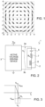
- Phase noise is more and more often becoming a critical aspect in voltage controlled oscillators, especially in wireless communication, as the huge growth in demand of band resources and frequency channels imposes very strict requirements to minimize communication errors. For example, in high-order phase shift keying (PSK) or quadrature amplitude modulation (QAM), phase noise may lead to errors in decoding adjacent symbols. As it can be understood from the example of
figure 1 , phase noise may cause carriers corresponding to given symbols to shift to amplitude and phase ranges of adjacent symbols, thus causing interpretation errors. - Phase noise reduction is therefore felt as a crucial goal to develop communication systems with higher capacity, due to wider bandwidth and spectrally efficient modulation schemes at up to millimeter wave carrier frequencies. According to a straightforward solution, phase noise in voltage controlled oscillators is reduced by scaling down the inductors of the parallel resonant circuit and increasing power consumption for a given supply voltage. However, the quality factor Q is degraded with too small inductors and sets a lower bound on phase noise.
- To overcome this limit, multi-core oscillators with parallel resonant circuits have been proposed, whereby N identical oscillators are coupled in a symmetric pattern to scale down phase noise by 10 log(N). Multi-core oscillators have been proved effective, but even minor mismatches between oscillators may significantly impair phase noise and penalize the figure of merit. Moreover, the required symmetric arrangement of the oscillators limits the number of cores that may be coupled together, thus also limiting the phase noise reduction that can be achieved. While in many applications multicore oscillators have provided a good solution, it cannot be expected that the strict requirements set by developments in telecommunications may be met.
- It is an object of the present invention to provide a voltage controlled oscillator that allows the above described limitations to be overcome or at least attenuated.
- According to the present invention, there is provided a voltage controlled oscillator as defined in
claim 1. - For a better understanding of the invention, some embodiments thereof will now be described, purely by way of non-limiting example and with reference to the attached drawings, wherein:
-
figure 1 is a graph showing effects of phase noise in a modulation scheme; -
figure 2 is a simplified block diagram of a voltage controlled oscillator in accordance with an embodiment of the present invention; -
figure 3 is a graph showing quantities of the voltage controlled oscillator offigure 2 ; -
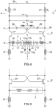
figure 4 is a circuit diagram of the voltage controlled oscillator offigure 2 ; -
figure 5 is a partial circuit diagram of a voltage controlled oscillator in accordance with a different embodiment of the present invention; -
figure 6 is a partial circuit diagram of a voltage controlled oscillator in accordance with another embodiment of the present invention; -
figure 7 is a block diagram of an electronic device including the voltage controlled oscillator offigure 6 . - With reference to
figure 2 , a voltage controlled oscillator in accordance with an embodiment of the present invention is designated bynumeral 1 and comprises a seriesresonant circuit 2 and an activevoltage driving device 3. - The series
resonant circuit 2 is coupled betweenvoltage supply terminals voltage driving device 3. More specifically, the seriesresonant circuit 2 comprises acapacitive component 5, aninductive component 6 and aresistive component 7 coupled in series between thevoltage supply terminals resistive component 7 also includes the resistances of thecapacitive component 5 and of theinductive component 6. Although it has been expressly indicated infigure 2 for the sake of clarity, a resistor as a separate component need not be included and theresistive component 7 may be defined exclusively by the resistances of thecapacitive component 5 and of theinductive component 6, in accordance with design preferences. A series resistance RS is associated with theresistive component 7. - The
series resonant circuit 2 is configured to resonate at a resonance frequency ω0 and has a series quality factor QS. In one example, the series quality factor QS is 15. - The active
voltage driving device 3 is configured to provide a driving voltage Vx and to have a negative resistance in an operative voltage range VR, as shown infigure 3 . Out of the operative voltage range VR, the driving voltage VX saturates to ±VMAX. At an equilibrium condition, both the driving voltage VX and a corresponding driving current Ix are zero and the negative resistance is selected with respect to the series resistance RS of the seriesresonant circuit 2 to allow build-up of oscillations. - With reference to
figure 4 , where the voltage controlledoscillator 1 is illustrated in greater detail, the seriesresonant circuit 2 is provided with atuning terminal 10 and abias terminal 11 coupled tobias nodes 11a through respective bias components,e.g. bias inductors 11b. In order to reduce voltage drop on each capacitive member, in one embodiment thecapacitive component 5 comprises a plurality ofcapacitors 12 and a pair oftuning varactors 13, coupled in series with one another symmetrically with respect to thetuning terminal 10. Specifically, thevaractors 13 have respective first terminals coupled to thetuning terminal 10 and second terminals coupled to a respective one of thebias nodes 11. Thecapacitors 12 are symmetrically coupled to thebias nodes varactors 13, to form a balanced capacitive structure. - In the embodiment of
figure 4 , theinductive component 6 comprises twoinductors 15, symmetrically coupled to opposite terminals of thecapacitive component 5 and further coupled to a respective one of thevoltage supply terminals voltage driving device 3. - The
resistive component 7 in turn comprises tworesistors 17, each in series with a respective one of theinductors 15. Theresistors 17 account for the resistance of therespective inductors 15 at the resonance frequency ω0 and may include additional separate components, in accordance with design preferences. For example, in low frequency applications, up to the kilohertz range, separate resistors may be provided, while at higher frequencies theresistive component 7 may be defined by the resistance of theinductors 15 alone. - The active
voltage driving device 3 comprises a cross-coupleddifferential pair 20,load resistors 21,choke inductors 23 andsaturator diodes - In the embodiment of
figure 4 , the cross-coupleddifferential pair 20 includesbipolar transistors 27 with respective base terminals coupled to collector terminals of the other transistor. Emitter terminals of thebipolar transistors 27 define thevoltage supply terminals voltage driving device 3. The collector terminals of thebipolar transistors 27 definecurrent supply terminals load resistors 21. It is understood that bipolar transistors may be replaced by field effect transistors in the cross-coupled differential pair, as illustrated infigure 5 , in which case thevoltage supply terminals current supply terminals -
Bias capacitors 28 in series with base terminals ofrespective transistors 27 andbias inductors 29 between the base terminals ofrespective transistors 27 and abias terminal 30 provide appropriate DC bias to prevent thetransistors 27 from operating in saturation region. Thechoke inductors 23 are in series with the emitter terminals ofrespective transistors 27 of the cross-coupleddifferential pair 20 and, beyond coupling a DC bias current component IB into the cross-coupleddifferential pair 20 to avoid saturation of thetransistors 27, allow the emitter terminals thereof, i.e. thevoltage supply terminals - The
load resistors 21 are coupled between the collector terminals ofrespective transistors 27 and avoltage supply line 32, providing a DC supply voltage VCC. The load resistors have a matched load resistance RL, whereby the differential output resistance R0 at thevoltage supply terminals 
figure 3 ), because of the action of the cross-coupleddifferential pair 20. Moreover, the load resistance RL is selected to meet the conditions to trigger oscillation build-up, namely
- The
saturator diodes transistors 27 and are selected to precisely set the boundaries of the operative voltage range VR, the maximum voltage value +VMAX and the minimum voltage value -VMAX for the driving voltage VX, as shown infigure 3 . - An estimation of phase noise associated with an oscillator at a given frequency offset Δω from the resonance frequency ω0 may be generally derived from Leeson's formula as follows:
 is the phase noise, F is the noise factor, k is the Boltzmann constant and Ps is the signal power associated with the resonant circuit of the oscillator.
- In the voltage-driven series
resonant circuit 2, the series signal power PSS is given by
- For a current-driven parallel resonant circuit with the same resistance, capacitance and inductance values as the series
resonant circuit 2, the same resonance frequency ω0 and a parallel quality factor QP equal to the series quality factor QS, the parallel signal power PSP is
- Hence

- Leeson's formula shows the reduction of phase noise provided by the voltage-driven series
resonant circuit 2 compared to dual current-driven parallel resonant circuits with the same circuit parameters, resonance frequency and quality factor:
- The reduction in phase noise is so significant that the voltage-driven series
resonant circuit 2 performs better than even dual current-driven parallel resonant circuits in multi-core configuration. Thus, on the one hand, the circuit structure and layout are simpler and much less chip area is occupied. On the other hand, the design of the voltage-driven seriesresonant circuit 2 is not limited by symmetry requirements, whereas oscillators based on the dual current-driven parallel resonant circuits must cope with the fact that increasing the number of cores beyond a few units may be very difficult, if at all possible. - The active
voltage driving device 3 provides appropriate driving voltage and also negative resistance capable of causing oscillations to build up through voltage supply terminals of the cross-coupled differential pair, i.e. emitter terminals (or source terminals for FETs). Thus, the voltage controlledoscillator 1 allows advantages of the seriesresonant circuit 2 to be exploited through a simple, yet effective and reliable driving. - For high-frequency applications, parasitic components play a role that in some cases may not be neglected. The solution of a series resonant circuit coupled to voltage supply terminals of an active voltage driving device based on a cross-coupled differential pair applies as well.
- According to the embodiment of
figure 6 , a voltage controlledoscillator 100 comprises a seriesresonant circuit 102 and an activevoltage driving device 103. - Substantially as already described with reference to
figure 2 and4 , the seriesresonant circuit 102 is coupled betweenvoltage supply terminals voltage driving device 103, and includes aseries capacitive component 105, a seriesinductive component 106 and a seriesresistive component 107. Furthermore, thecircuit 102 has a resonance frequency ω0 (e.g. 10 GHz) and a series quality factor QS. Here, the seriesresistive component 107 substantially coincides with a parasitic series resistance RS of the seriesinductive component 106 at the resonance frequency ω0. The seriesresistive component 107 may have the same structure as theresistive component 7 offigure 4 . - The active
voltage driving device 103 is configured to provide a driving voltage Vx and to have a negative resistance with a V-I characteristic qualitatively similar to the one shown infigure 3 . - The active
voltage driving device 103 comprises a cross-coupleddifferential pair 120, a parallelresonant circuit 121, choke inductors 123 and saturator diodes 125, 126. - The cross-coupled
differential pair 20 includesbipolar transistors 127 with respective base terminals coupled to collector terminals of the other transistor. Emitter terminals of thebipolar transistors 127 define thevoltage supply terminals voltage driving device 3. The collector terminals of thebipolar transistors 127 definecurrent supply terminals resonant circuit 121. - Bias components, not shown here, may be provided to apply appropriate DC bias to prevent the
transistors 127 from operating in saturation region. The choke inductors 123 are coupled between the emitter terminals ofrespective transistors 127 of the cross-coupleddifferential pair 120 and ground and, beyond coupling a DC bias current component IB to the cross-coupleddifferential pair 120 to avoid saturation of thetransistors 127, allow the emitter terminals thereof, i.e. thevoltage supply terminals - The parallel
resonant circuit 121 is coupled between the collector terminals of thetransistors 127 and includes aparallel capacitive component 128, a parallelinductive component 129 and a parallelresistive component 130. - The
parallel capacitive component 128 accounts for parasitic capacitances at collector terminals of thetransistors 127, i.e. atcurrent supply terminals - The parallel
inductive component 129 is selected to tune a resonance frequency of the parallelresonant circuit 121 at the series resonance frequency ω 0 of the seriesresonant circuit 102. A center point of the parallelinductive component 129 is coupled to avoltage supply line 132, providing a DC supply voltage VCC. - The parallel
resistive component 130 may be essentially determined by the parasitic resistance of the parallelinductive component 129 and is selected to meet the condition for build-up of oscillations in the seriesresonant circuit 103 at the series resonance frequency ω 0. More precisely, the parallel resistance Rp of the parallelresistive component 130 at the series resonance frequency ω 0 is selected such that the differential output resistance Ro at thevoltage supply terminals 

- The saturator diodes 125, 126 are coupled in anti-parallel configuration between the collector terminals of the
transistors 127 and are selected to precisely set the boundaries of the operative voltage range VR and the maximum voltage value +VMAX and the minimum voltage value -VMAX for the driving voltage VX, as shown infigure 3 . - At the resonance frequency ω 0, oscillation of the voltage controlled
oscillator 100 is dominated by the seriesresonant circuit 102. The parallelresonant circuit 121 tunes at the resonance frequency ω 0 as well and, in resonance conditions, the associated impedance is in fact the parallel resistance Rp of the parallelresistive component 130. In practice, the parallelresonant circuit 121 is exploited to cancel effects of parasitic components so that, at the resonance frequency ω 0, the parallelresonant circuit 121 defines a purely resistive load and the impedance results in the negative resistance required to build up and sustain oscillation. Operation at very high frequency is thus allowed and reduction of phase noise associated with the voltage-driven seriesresonant circuit 102 may be preserved. - As an example, in
figure 7 the voltage controlledoscillator 100 is configured to oscillate at a resonance frequency ω 0 of 10 GHz and is coupled to afrequency multiplier 150, which provides frequency increase by a factor of 8. Acontrol unit 160 controls operation of the voltage controlledoscillator 100, e.g. provides for enabling/disabling operation, tuning, testing and the like. - For the voltage controlled
oscillator 100, phase noise at 1 MHz off the resonance frequency is -138 dBc/Hz, which results in -120 dBc/Hz at 80 GHz at the output of thefrequency multiplier 150. The above level of phase noise allows the following modulation schemes to be implemented for example:Modulation 
QPSK -90 dBc/Hz 16 QAM -96 dBc/Hz 64 QAM -102 dBc/Hz 256 QAM -108 dBc/Hz 1024 QAM -114 dBc/Hz 4096 QAM -120 dBc/Hz - Finally, it is evident that modifications and variations may be made to the voltage controlled oscillator described, without thereby departing from the scope of the present invention, as defined in the annexed claims.
Claims (15)
- A voltage controlled oscillator comprising:a series resonant circuit (2; 102), having a resonance frequency (ω 0);an active voltage driving device (3; 103), coupled to the series resonant circuit (2; 102) and configured to provide a driving voltage (Vx) and to have an output negative resistance (Ro) in an operative voltage range (VR) at the resonance frequency (ω 0);wherein the active voltage driving device (3; 103) comprises a cross-coupled differential pair (20; 20'; 120) having voltage supply terminals (3a, 3b; 103a, 103b) and the series resonant circuit (2; 102) is coupled to the voltage supply terminals (3a, 3b; 103a, 103b) of the cross-coupled differential pair (20; 20'; 120).
- The oscillator according to claim 1, wherein the cross-coupled differential pair (20; 20'; 120) comprises a pair of transistors (27; 27'; 127) in differential follower configuration and the voltage supply terminals (3a, 3b; 103a, 103b) are defined by output conduction terminals of the transistors (27; 27'; 127).
- The oscillator according to claim 2, wherein the transistors (27; 127) are bipolar transistors and the voltage supply terminals (3a, 3b; 103a, 103b) are defined by emitter terminals of the transistors (27; 127); or wherein the transistors (27') are field effect transistors and the voltage supply terminals (3a, 3b; 103a, 103b) are defined by source terminals of the transistors (27').
- The oscillator according to any one of the preceding claims, wherein the cross-coupled differential pair (20; 20'; 120) has current supply terminals (3c, 3d; 103c, 103d) and the active voltage driving device (3; 103) comprises a load (21; 121) coupled to the current supply terminals (3c, 3d; 103c, 103d), wherein the load (21; 121) is a resistive load at the resonance frequency (ω 0).
- The oscillator according to claim 4, wherein the load (21) comprises resistors coupled to the current supply terminals (3c, 3d) of the cross-coupled differential pair (20; 20'; 120).
- The oscillator according to claim 4, wherein the load (121) comprises a parallel resonant circuit coupled to the current supply terminals (103c, 103d) of the cross-coupled differential pair (20; 20'; 120) and tuned at the resonance frequency (ω 0).
- The oscillator according to claim 6, wherein the parallel resonant circuit (121) comprises a parallel capacitive component (128) and wherein parasitic capacitances of the transistors (127) form at least part of the parallel capacitive component (128).
- The oscillator according to claim 7, wherein the parallel resonant circuit (121) comprises a parallel inductive component (129) selected to tune the parallel resonant circuit (121) at the series resonance frequency (ω 0).
- The oscillator according to claim 8, wherein a center point of the parallel inductive component (129) is coupled to a voltage supply line (132) configured to provide a DC supply voltage (VCC).
- The oscillator according to claim 8 or 9, wherein the parallel resonant circuit (121) comprises a parallel resistive component (130) that includes a parasitic resistance of the parallel inductive component (129).
- The oscillator according to any one of claims 4 to 10, wherein the series resonant circuit (2; 102) has a series resistance (RS) and wherein the load (21; 121) is selected such that, at the resonance frequency (ω0), an absolute value of the output negative resistance (R0) of the active voltage driving device (3; 103) is greater than the series resistance (RS) of the series resonant circuit (2; 102).
- The oscillator according to any one of claims 4 to 11, wherein the active voltage driving device (3; 103) comprises a first saturator diode (25) and a second saturator diode (26) coupled in anti-parallel configuration between the current supply terminals (3c, 3d; 103c, 103d) of the active voltage driving device (3; 103)
- The oscillator according to any one of claims 2 to 12, wherein the active voltage driving device (3; 103) comprises bias components coupled between the output conduction terminals of respective transistors (27; 27'; 127) of the cross-coupled differential pair (120) and a reference voltage line and are configured to couple a DC bias current component (IB) into the cross-coupled differential pair (20; 120) to avoid saturation of the transistors (27; 127).
- An electronic system comprising a voltage controlled oscillator (100) according to any one of the preceding claims and a control unit (160) coupled to the voltage controlled oscillator (100).
- The electronic system according to claim 14, comprising a frequency multiplier (150) coupled to the voltage controlled oscillator (100) and configured to multiply the resonance frequency (ω) by a multiplying factor.
Applications Claiming Priority (1)
| Application Number | Priority Date | Filing Date | Title |
|---|---|---|---|
| IT102021000023000A IT202100023000A1 (en) | 2021-09-06 | 2021-09-06 | VOLTAGE CONTROLLED OSCILLATOR WITH SERIES RESONANT CIRCUIT |
Publications (1)
| Publication Number | Publication Date |
|---|---|
| EP4145706A1 true EP4145706A1 (en) | 2023-03-08 |
Family
ID=78770925
Family Applications (1)
| Application Number | Title | Priority Date | Filing Date |
|---|---|---|---|
| EP22191733.9A Pending EP4145706A1 (en) | 2021-09-06 | 2022-08-23 | Voltage controlled oscillator with series resonant circuit |
Country Status (3)
| Country | Link |
|---|---|
| US (1) | US11936339B2 (en) |
| EP (1) | EP4145706A1 (en) |
| IT (1) | IT202100023000A1 (en) |
Families Citing this family (2)
| Publication number | Priority date | Publication date | Assignee | Title |
|---|---|---|---|---|
| CN119543834B (en) * | 2024-11-20 | 2026-03-17 | 重庆邮电大学 | A CMOS voltage-controlled oscillator for anti-jamming UAV millimeter-wave radar |
| US12615016B1 (en) | 2024-12-17 | 2026-04-28 | Nxp Usa, Inc. | Series resonance oscillator |
Citations (5)
| Publication number | Priority date | Publication date | Assignee | Title |
|---|---|---|---|---|
| EP2034609A2 (en) * | 2007-09-10 | 2009-03-11 | Hitachi Ltd. | Oscillator and communication system using the same |
| JP2010193271A (en) * | 2009-02-19 | 2010-09-02 | Mitsubishi Electric Corp | Differential output oscillator |
| US20130154752A1 (en) * | 2011-12-14 | 2013-06-20 | Taiwan Semiconductor Manufacturing Company, Ltd. | Voltage-controlled oscillator |
| WO2016164875A1 (en) * | 2015-04-09 | 2016-10-13 | Texas Instruments Incorporated | Low-power low-phase-noise oscillator |
| US20170047890A1 (en) * | 2014-12-24 | 2017-02-16 | National Chi Nan University | Voltage-controlled oscillator |
Family Cites Families (4)
| Publication number | Priority date | Publication date | Assignee | Title |
|---|---|---|---|---|
| US4353039A (en) * | 1980-05-15 | 1982-10-05 | Gte Automatic Electric Laboratories, Inc. | Monolithic astable multivibrator circuit |
| US6972635B2 (en) * | 2002-02-26 | 2005-12-06 | The Regents Of The University Of Michigan | MEMS-based, computer systems, clock generation and oscillator circuits and LC-tank apparatus for use therein |
| ITUB20154230A1 (en) | 2015-10-08 | 2017-04-08 | St Microelectronics Srl | CIRCUIT OSCILLATOR, EQUIPMENT AND CORRESPONDENT PROCEDURE " |
| US11228280B1 (en) * | 2021-02-01 | 2022-01-18 | Texas Instruments Incorporated | Microelectromechanical system resonator-based oscillator |
-
2021
- 2021-09-06 IT IT102021000023000A patent/IT202100023000A1/en unknown
-
2022
- 2022-08-23 EP EP22191733.9A patent/EP4145706A1/en active Pending
- 2022-08-24 US US17/894,548 patent/US11936339B2/en active Active
Patent Citations (5)
| Publication number | Priority date | Publication date | Assignee | Title |
|---|---|---|---|---|
| EP2034609A2 (en) * | 2007-09-10 | 2009-03-11 | Hitachi Ltd. | Oscillator and communication system using the same |
| JP2010193271A (en) * | 2009-02-19 | 2010-09-02 | Mitsubishi Electric Corp | Differential output oscillator |
| US20130154752A1 (en) * | 2011-12-14 | 2013-06-20 | Taiwan Semiconductor Manufacturing Company, Ltd. | Voltage-controlled oscillator |
| US20170047890A1 (en) * | 2014-12-24 | 2017-02-16 | National Chi Nan University | Voltage-controlled oscillator |
| WO2016164875A1 (en) * | 2015-04-09 | 2016-10-13 | Texas Instruments Incorporated | Low-power low-phase-noise oscillator |
Also Published As
| Publication number | Publication date |
|---|---|
| US11936339B2 (en) | 2024-03-19 |
| US20230081414A1 (en) | 2023-03-16 |
| IT202100023000A1 (en) | 2023-03-06 |
Similar Documents
| Publication | Publication Date | Title |
|---|---|---|
| US7920030B2 (en) | Multi-phase voltage-control oscillator | |
| US7088189B2 (en) | Integrated low noise microwave wideband push-push VCO | |
| US8067995B2 (en) | Voltage controlled oscillator, and PLL circuit and wireless communication device each using the same | |
| US20100271086A1 (en) | Dual-band coupled vco | |
| JP4089938B2 (en) | Voltage controlled oscillator | |
| US20080284534A1 (en) | Oscillator | |
| US11936339B2 (en) | Voltage controlled oscillator with series resonant circuit | |
| US6661301B2 (en) | Oscillator circuit | |
| US20020093385A1 (en) | Oscillation circuit with voltage-controlled oscillators | |
| EP1542354B1 (en) | Integrated ultra low noise microwave wideband push-push vco | |
| US6545555B1 (en) | Voltage controlled oscillator having a phase noise reduction device | |
| WO2005057790A2 (en) | Integrated low noise microwave wideband push-push vco | |
| US9099957B2 (en) | Voltage-controlled oscillators and related systems | |
| US6486744B1 (en) | Low phase noise voltage-controlled oscillator and method of using the same | |
| JP4825860B2 (en) | Low noise voltage controlled oscillator | |
| US8264295B2 (en) | Switched varactor circuit for a voltage controlled oscillator | |
| CN115765630A (en) | Voltage controlled oscillator with series resonant circuit | |
| US6842081B2 (en) | Dual frequency voltage controlled oscillator circuit | |
| KR20090054784A (en) | Capacitive Degeneration Double Cross-Coupled Voltage Controlled Oscillators | |
| JP4545737B2 (en) | Oscillator circuit | |
| US6690244B2 (en) | Low phase-noise integrated voltage controlled oscillator | |
| KR20090077510A (en) | Voltage Controlled Oscillators Using WLSL | |
| KR100286465B1 (en) | Oscillating circuit | |
| EP1902518B1 (en) | Voltage controlled oscillator with simultaneous switching of frequency band, oscillation core and varactor size | |
| CA2533623C (en) | Tunable oscillator |
Legal Events
| Date | Code | Title | Description |
|---|---|---|---|
| PUAI | Public reference made under article 153(3) epc to a published international application that has entered the european phase |
Free format text: ORIGINAL CODE: 0009012 |
|
| STAA | Information on the status of an ep patent application or granted ep patent |
Free format text: STATUS: THE APPLICATION HAS BEEN PUBLISHED |
|
| AK | Designated contracting states |
Kind code of ref document: A1 Designated state(s): AL AT BE BG CH CY CZ DE DK EE ES FI FR GB GR HR HU IE IS IT LI LT LU LV MC MK MT NL NO PL PT RO RS SE SI SK SM TR |
|
| STAA | Information on the status of an ep patent application or granted ep patent |
Free format text: STATUS: REQUEST FOR EXAMINATION WAS MADE |
|
| 17P | Request for examination filed |
Effective date: 20230908 |
|
| RBV | Designated contracting states (corrected) |
Designated state(s): AL AT BE BG CH CY CZ DE DK EE ES FI FR GB GR HR HU IE IS IT LI LT LU LV MC MK MT NL NO PL PT RO RS SE SI SK SM TR |
|
| STAA | Information on the status of an ep patent application or granted ep patent |
Free format text: STATUS: EXAMINATION IS IN PROGRESS |
|
| 17Q | First examination report despatched |
Effective date: 20241120 |