EP4145524A1 - Display panel - Google Patents
Display panel Download PDFInfo
- Publication number
- EP4145524A1 EP4145524A1 EP20917292.3A EP20917292A EP4145524A1 EP 4145524 A1 EP4145524 A1 EP 4145524A1 EP 20917292 A EP20917292 A EP 20917292A EP 4145524 A1 EP4145524 A1 EP 4145524A1
- Authority
- EP
- European Patent Office
- Prior art keywords
- layer
- phase retardation
- display panel
- thin film
- linear polarizing
- Prior art date
- Legal status (The legal status is an assumption and is not a legal conclusion. Google has not performed a legal analysis and makes no representation as to the accuracy of the status listed.)
- Pending
Links
Images
Classifications
-
- H—ELECTRICITY
- H10—SEMICONDUCTOR DEVICES; ELECTRIC SOLID-STATE DEVICES NOT OTHERWISE PROVIDED FOR
- H10K—ORGANIC ELECTRIC SOLID-STATE DEVICES
- H10K59/00—Integrated devices, or assemblies of multiple devices, comprising at least one organic light-emitting element covered by group H10K50/00
- H10K59/80—Constructional details
- H10K59/8791—Arrangements for improving contrast, e.g. preventing reflection of ambient light
-
- H—ELECTRICITY
- H10—SEMICONDUCTOR DEVICES; ELECTRIC SOLID-STATE DEVICES NOT OTHERWISE PROVIDED FOR
- H10K—ORGANIC ELECTRIC SOLID-STATE DEVICES
- H10K50/00—Organic light-emitting devices
- H10K50/80—Constructional details
- H10K50/86—Arrangements for improving contrast, e.g. preventing reflection of ambient light
-
- G—PHYSICS
- G02—OPTICS
- G02B—OPTICAL ELEMENTS, SYSTEMS OR APPARATUS
- G02B5/00—Optical elements other than lenses
- G02B5/30—Polarising elements
- G02B5/3016—Polarising elements involving passive liquid crystal elements
-
- H—ELECTRICITY
- H10—SEMICONDUCTOR DEVICES; ELECTRIC SOLID-STATE DEVICES NOT OTHERWISE PROVIDED FOR
- H10K—ORGANIC ELECTRIC SOLID-STATE DEVICES
- H10K50/00—Organic light-emitting devices
- H10K50/80—Constructional details
- H10K50/84—Passivation; Containers; Encapsulations
- H10K50/844—Encapsulations
-
- H—ELECTRICITY
- H10—SEMICONDUCTOR DEVICES; ELECTRIC SOLID-STATE DEVICES NOT OTHERWISE PROVIDED FOR
- H10K—ORGANIC ELECTRIC SOLID-STATE DEVICES
- H10K50/00—Organic light-emitting devices
- H10K50/80—Constructional details
- H10K50/86—Arrangements for improving contrast, e.g. preventing reflection of ambient light
- H10K50/865—Arrangements for improving contrast, e.g. preventing reflection of ambient light comprising light absorbing layers, e.g. light-blocking layers
-
- H—ELECTRICITY
- H10—SEMICONDUCTOR DEVICES; ELECTRIC SOLID-STATE DEVICES NOT OTHERWISE PROVIDED FOR
- H10K—ORGANIC ELECTRIC SOLID-STATE DEVICES
- H10K59/00—Integrated devices, or assemblies of multiple devices, comprising at least one organic light-emitting element covered by group H10K50/00
- H10K59/10—OLED displays
- H10K59/12—Active-matrix OLED [AMOLED] displays
-
- H—ELECTRICITY
- H10—SEMICONDUCTOR DEVICES; ELECTRIC SOLID-STATE DEVICES NOT OTHERWISE PROVIDED FOR
- H10K—ORGANIC ELECTRIC SOLID-STATE DEVICES
- H10K59/00—Integrated devices, or assemblies of multiple devices, comprising at least one organic light-emitting element covered by group H10K50/00
- H10K59/80—Constructional details
- H10K59/87—Passivation; Containers; Encapsulations
- H10K59/873—Encapsulations
- H10K59/8731—Encapsulations multilayered coatings having a repetitive structure, e.g. having multiple organic-inorganic bilayers
-
- H—ELECTRICITY
- H10—SEMICONDUCTOR DEVICES; ELECTRIC SOLID-STATE DEVICES NOT OTHERWISE PROVIDED FOR
- H10K—ORGANIC ELECTRIC SOLID-STATE DEVICES
- H10K59/00—Integrated devices, or assemblies of multiple devices, comprising at least one organic light-emitting element covered by group H10K50/00
- H10K59/80—Constructional details
- H10K59/8791—Arrangements for improving contrast, e.g. preventing reflection of ambient light
- H10K59/8792—Arrangements for improving contrast, e.g. preventing reflection of ambient light comprising light absorbing layers, e.g. black layers
-
- H—ELECTRICITY
- H10—SEMICONDUCTOR DEVICES; ELECTRIC SOLID-STATE DEVICES NOT OTHERWISE PROVIDED FOR
- H10K—ORGANIC ELECTRIC SOLID-STATE DEVICES
- H10K59/00—Integrated devices, or assemblies of multiple devices, comprising at least one organic light-emitting element covered by group H10K50/00
- H10K59/80—Constructional details
- H10K59/8793—Arrangements for polarized light emission
-
- G—PHYSICS
- G02—OPTICS
- G02B—OPTICAL ELEMENTS, SYSTEMS OR APPARATUS
- G02B5/00—Optical elements other than lenses
- G02B5/30—Polarising elements
- G02B5/3083—Birefringent or phase retarding elements
-
- G—PHYSICS
- G02—OPTICS
- G02F—OPTICAL DEVICES OR ARRANGEMENTS FOR THE CONTROL OF LIGHT BY MODIFICATION OF THE OPTICAL PROPERTIES OF THE MEDIA OF THE ELEMENTS INVOLVED THEREIN; NON-LINEAR OPTICS; FREQUENCY-CHANGING OF LIGHT; OPTICAL LOGIC ELEMENTS; OPTICAL ANALOGUE/DIGITAL CONVERTERS
- G02F1/00—Devices or arrangements for the control of the intensity, colour, phase, polarisation or direction of light arriving from an independent light source, e.g. switching, gating or modulating; Non-linear optics
- G02F1/01—Devices or arrangements for the control of the intensity, colour, phase, polarisation or direction of light arriving from an independent light source, e.g. switching, gating or modulating; Non-linear optics for the control of the intensity, phase, polarisation or colour
- G02F1/13—Devices or arrangements for the control of the intensity, colour, phase, polarisation or direction of light arriving from an independent light source, e.g. switching, gating or modulating; Non-linear optics for the control of the intensity, phase, polarisation or colour based on liquid crystals, e.g. single liquid crystal display cells
- G02F1/133—Constructional arrangements; Operation of liquid crystal cells; Circuit arrangements
- G02F1/1333—Constructional arrangements; Manufacturing methods
- G02F1/1335—Structural association of cells with optical devices, e.g. polarisers or reflectors
- G02F1/133509—Filters, e.g. light shielding masks
- G02F1/133512—Light shielding layers, e.g. black matrix
-
- G—PHYSICS
- G02—OPTICS
- G02F—OPTICAL DEVICES OR ARRANGEMENTS FOR THE CONTROL OF LIGHT BY MODIFICATION OF THE OPTICAL PROPERTIES OF THE MEDIA OF THE ELEMENTS INVOLVED THEREIN; NON-LINEAR OPTICS; FREQUENCY-CHANGING OF LIGHT; OPTICAL LOGIC ELEMENTS; OPTICAL ANALOGUE/DIGITAL CONVERTERS
- G02F1/00—Devices or arrangements for the control of the intensity, colour, phase, polarisation or direction of light arriving from an independent light source, e.g. switching, gating or modulating; Non-linear optics
- G02F1/01—Devices or arrangements for the control of the intensity, colour, phase, polarisation or direction of light arriving from an independent light source, e.g. switching, gating or modulating; Non-linear optics for the control of the intensity, phase, polarisation or colour
- G02F1/13—Devices or arrangements for the control of the intensity, colour, phase, polarisation or direction of light arriving from an independent light source, e.g. switching, gating or modulating; Non-linear optics for the control of the intensity, phase, polarisation or colour based on liquid crystals, e.g. single liquid crystal display cells
- G02F1/133—Constructional arrangements; Operation of liquid crystal cells; Circuit arrangements
- G02F1/136—Liquid crystal cells structurally associated with a semi-conducting layer or substrate, e.g. cells forming part of an integrated circuit
- G02F1/1362—Active matrix addressed cells
- G02F1/136209—Light shielding layers, e.g. black matrix, incorporated in the active matrix substrate, e.g. structurally associated with the switching element
-
- H—ELECTRICITY
- H10—SEMICONDUCTOR DEVICES; ELECTRIC SOLID-STATE DEVICES NOT OTHERWISE PROVIDED FOR
- H10K—ORGANIC ELECTRIC SOLID-STATE DEVICES
- H10K2102/00—Constructional details relating to the organic devices covered by this subclass
- H10K2102/301—Details of OLEDs
- H10K2102/311—Flexible OLED
-
- H—ELECTRICITY
- H10—SEMICONDUCTOR DEVICES; ELECTRIC SOLID-STATE DEVICES NOT OTHERWISE PROVIDED FOR
- H10K—ORGANIC ELECTRIC SOLID-STATE DEVICES
- H10K2102/00—Constructional details relating to the organic devices covered by this subclass
- H10K2102/301—Details of OLEDs
- H10K2102/351—Thickness
-
- H—ELECTRICITY
- H10—SEMICONDUCTOR DEVICES; ELECTRIC SOLID-STATE DEVICES NOT OTHERWISE PROVIDED FOR
- H10K—ORGANIC ELECTRIC SOLID-STATE DEVICES
- H10K50/00—Organic light-emitting devices
- H10K50/80—Constructional details
- H10K50/868—Arrangements for polarized light emission
-
- H—ELECTRICITY
- H10—SEMICONDUCTOR DEVICES; ELECTRIC SOLID-STATE DEVICES NOT OTHERWISE PROVIDED FOR
- H10K—ORGANIC ELECTRIC SOLID-STATE DEVICES
- H10K77/00—Constructional details of devices covered by this subclass and not covered by groups H10K10/80, H10K30/80, H10K50/80 or H10K59/80
- H10K77/10—Substrates, e.g. flexible substrates
-
- H—ELECTRICITY
- H10—SEMICONDUCTOR DEVICES; ELECTRIC SOLID-STATE DEVICES NOT OTHERWISE PROVIDED FOR
- H10K—ORGANIC ELECTRIC SOLID-STATE DEVICES
- H10K77/00—Constructional details of devices covered by this subclass and not covered by groups H10K10/80, H10K30/80, H10K50/80 or H10K59/80
- H10K77/10—Substrates, e.g. flexible substrates
- H10K77/111—Flexible substrates
Definitions
- the present disclosure relates to the field of display technology, and particularly, to a display panel.
- a polarizer of the OLED display screen is composed of a ⁇ /4 phase retardation sheet and a linear polarizer, and the polarizer may effectively eliminate reflected light caused by external light irradiating a surface of the display screen.
- a thickness of the conventional polarizer is generally less than 100 ⁇ m, thereby limiting the thickness of the screen and reducing bending performance of the screen.
- the present disclosure provides a display panel to solve a problem in conventional display panels that disposition of a polarizer limits a thickness of the entire display panel and reduces bending performance of the display panel.
- the present disclosure provides technical solutions as follows:
- the present disclosure provides a display panel including:
- the thin film encapsulation layer includes inorganic layers and an organic layer which are mutually stacked, and the phase retardation layer and the linear polarizing layer are located between the inorganic layer and the organic layer which are adjacent to each other, or the inorganic layer and/or the organic layer are disposed between the phase retardation layer and the linear polarizing layer.
- the linear polarizing layer is located on a side of the phase retardation layer away from the light emitting device layer.
- the light-emitting layer includes light emitting devices distributed in an array
- the phase retardation layer includes phase retardation units corresponding to the light emitting devices and distributed in an array
- the display panel is provided with black barrier walls corresponding to gaps between the two adjacent phase retardation units.
- the thin film transistor array layer includes an inorganic stacked layer and thin film transistors
- the display panel is further provided with an organic stacked layer on the inorganic stacked layer
- the black barrier walls are located on the organic stacked layer or within the thin film encapsulation layer.
- the linear polarizing layer includes linear polarizing units corresponding to the phase retardation units and distributed in an array, and orthographic projections of the linear polarizing units projected on the substrate cover orthographic projections of the phase retardation units projected on the substrate.
- the phase retardation units cover a light emitting area of the light emitting device layer.
- the phase retardation layer is made of an anisotropic organic material.
- the phase retardation layer is made of a liquid crystal material, and alignment layers are disposed on a surface of the phase retardation layer.
- a phase difference of the phase retardation layer is a quarter wavelength.
- the present disclosure further provides a display panel including:
- the thin film encapsulation layer includes inorganic layers and an organic layer which are mutually stacked, and the phase retardation layer and the linear polarizing layer are located between the inorganic layer and the organic layer which are adjacent to each other, or the inorganic layer and/or the organic layer are disposed between the phase retardation layer and the linear polarizing layer.
- the linear polarizing layer is located on a side of the phase retardation layer away from the light emitting device layer.
- the light-emitting layer includes light emitting devices distributed in an array
- the phase retardation layer includes phase retardation units corresponding to the light emitting devices and distributed in an array
- the display panel is provided with black barrier walls corresponding to gaps between the two adjacent phase retardation units.
- the thin film transistor array layer includes an inorganic stacked layer and thin film transistors
- the display panel is further provided with an organic stacked layer on the inorganic stacked layer
- the black barrier walls are located on the organic stacked layer or within the thin film encapsulation layer.
- the linear polarizing layer includes linear polarizing units corresponding to the phase retardation units and distributed in an array, and orthographic projections of the linear polarizing units projected on the substrate cover orthographic projections of the phase retardation units projected on the substrate.
- the phase retardation units cover a light emitting area of the light emitting device layer.
- the phase retardation layer is made of an anisotropic organic material.
- the phase retardation layer is made of a liquid crystal material, and alignment layers are disposed on a surface of the phase retardation layer.
- a phase difference of the phase retardation layer is a quarter wavelength.
- a thickness of the display panel provides by the present disclosure is greatly reduced by removing the conventional polarizer and disposing the phase retardation layer and the linear polarizing layer within the thin film encapsulation layer, thus improving the bending performance of the display panel.
- the combination of the phase retardation layer and the linear polarizing layer may effectively eliminate reflected light caused by external light irradiating a surface of the display panel.
- indicative directions or position relations such as terms “longitudinal”, “transverse”, “length”, “width”, “upper”, “lower”, “front”, “back”, “left”, “right”, “vertical”, and “horizontal”, are based on directions or position relations indicated by the accompanying drawings.
- the indicative directions or position relations are only for convenience of describing the present disclosure and simplifying the description, and do not indicate or imply that indicated devices or elements must have a specific orientation and be constructed and operated in a specific orientation. Therefore, the indicative directions or position relations cannot be understood to be limitation to the present disclosure.
- first and second are only used for purposes of description, and do not be understood to indicate or imply relative importance or to imply numbers of indicated technical features. Thus, the features defined with “first” and “second” may explicitly or implicitly include one or more of the features.
- term “a plurality of” means two or more than two, unless specified otherwise. In the present disclosure, “/" means “or”.
- the present disclosure provides a display panel including a substrate 10 which may be a flexible substrate, but not limited to the flexible substrate, a thin film transistor array layer 20 disposed on the substrate 10, a light emitting device layer 40 disposed on the thin film transistor array layer 20, a thin film encapsulation layer 50 disposed on the light emitting device layer 40, a phase retardation layer 60 disposed within the thin film encapsulation layer 50, and a linear polarizing layer 70 disposed within the thin film encapsulation layer 50, wherein the phase retardation layer 60 and the linear polarizing layer 70 are mutually stacked.
- a substrate 10 which may be a flexible substrate, but not limited to the flexible substrate
- a thin film transistor array layer 20 disposed on the substrate 10
- a light emitting device layer 40 disposed on the thin film transistor array layer 20
- a thin film encapsulation layer 50 disposed on the light emitting device layer 40
- a phase retardation layer 60 disposed within the thin film encapsulation layer 50
- the conventional organic light-emitting diode (OLED) display panels usually employ external polarizers.
- the polarizer generally is a composite film composed of a plurality of organic material layers including the ⁇ /4 phase retardation layer and the linear polarizing layer, and these two birefringent layers may achieve an anti-reflection function of the screen.
- a plurality of thin films are required to protect and connect the ⁇ /4 phase retardation layer with the linear polarizing layer, thus resulting in the polarizer with a great thickness.
- the thickness of the conventional polarizer is generally less than 100 ⁇ m, thereby limiting a thickness of the screen and reducing bending performance of the screen.
- the combination of the phase retardation layer and the linear polarizing layer may effectively eliminate reflected light caused by external light irradiating a surface of the display panel.
- a thickness of the display panel of the present disclosure is greatly reduced, thereby improving the bending performance of the display panel and facilitating the development of the foldable display panels.
- the display panel described by the present disclosure is illustrated in detail below.
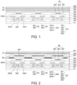
- FIG. 1 is a structural schematic view of a display panel provided by the first embodiment of the present disclosure.
- the thin film transistor array layer 20 is disposed on the substrate 10 and includes an inorganic stacked layer and thin film transistors 204.
- the inorganic stacked layer includes, but is not limited to, a first gate insulation layer 201, a second gate insulation layer 202, and an interlayer insulation layer 203 which are mutually stacked.
- the thin film transistor 204 includes an active layer 2041, a gate electrode 2042, and a source/drain electrode 2043.
- An electrode layer 205 is disposed on the gate electrode 2042 and is insulated from the gate electrode 2042, and the electrode layer 205 and the gate electrode 2042 form an electric capacity.
- An organic stacked layer 30 and the light emitting device layer 40 are also disposed on the inorganic stacked layer, and the organic stacked layer 30 includes, but is not limited to, a planarization layer 301 and a pixel definition layer 302 which are mutually stacked.
- the light emitting device layer 40 includes anodes 401, light emitting layers 402, a cathode 403 which are mutually stacked.
- the anodes 401 are disposed on the planarization layer 301, and are electrically connected to the source/drain electrodes 2043 of the thin film transistors 204 via through holes on the planarization layer 301. Pixel holes are formed on sites of the pixel definition layer 302 corresponding to the anodes 401, the light emitting layers 402 are located within the pixel holes, and the cathode 403 is disposed on the light emitting layers 402.
- the thin film encapsulation layer 50 is disposed on the cathode 403, and at least includes three laminated layers which are an inorganic layer 501, an organic layer 502, and an inorganic layer 501.
- a thickness of the inorganic layer is generally in a range of several hundred nanometers, and a thickness of the organic layer 502 is generally less than 20 ⁇ m.
- the organic layer 502 may not only be used to block water and oxygen but also function as a flat surface.
- the external polarizer is integrated into the thin film encapsulation layer 50 of the display panel in the present disclosure.
- the thin film encapsulation layer 50 includes the phase retardation layer 60 and the linear polarizing layer 70, and the linear polarizing layer 70 is located on a side of the phase retardation layer 60 away from the light emitting device layer 40.
- the whole phase retardation layer 60 and the whole linear polarizing layer 70 are disposed within the thin film encapsulation layer 50.
- the inorganic layer 501 and/or the organic layer 502 are disposed between the phase retardation layer 60 and the linear polarizing layer 70, or the phase retardation layer 60 and the linear polarizing layer 70 are located between the inorganic layer and the organic layer which are adjacent to each other.
- the phase retardation layer 60 is located on a first inorganic layer 501
- the organic layer 502 is disposed on the phase retardation layer 60
- the linear polarizing layer 70 is disposed on the organic layer 502
- a second inorganic layer 501 is disposed on the linear polarizing layer 70.
- a phase difference of the phase retardation layer 60 is a quarter wavelength, and the phase retardation layer 60 may be a quarter wave plate.
- the external incident light or nature light when the external incident light or nature light irradiates the surface of the display panel, the external incident light or nature light passes through the linear polarizing layer 70 to be converted into linearly polarized light, such as the linearly polarized light in a horizontal direction, the linearly polarized light passed through the phase retardation layer 60 to be converted into circularly polarized light, and the circularly polarized light is reflected by the cathode 403 and the anodes 401, thus increasing the phase difference of ⁇ .
- left-handed circularly polarized light is converted into right-handed circularly polarized light, or the right-handed circularly polarized light is converted into the left-handed circularly polarized light.
- the circularly polarized light with the phase retardation passes through the phase retardation layer 60 again to be converted into the linearly polarized light perpendicular to the incident linearly polarized light, such as the linearly polarized light in a vertical direction, so that the linearly polarized light in the vertical direction cannot pass through the linear polarizing layer 70, thus achieving the elimination of the light.
- the quarter wave plate of the conventional polarizer is mainly obtained by stretching polymer material, a thickness of the quarter wave plate generally requires to be several ten microns to reach a specific coefficient of the phase retardation.
- the phase retardation layer 60 may be made of a liquid crystal material or other anisotropic organic materials, and a thickness of the phase retardation layer 60 is in a range of one to several microns, thereby greatly reducing the thickness and improving the bending performance of the display panel.
- FIG. 2 is a structural schematic view of a display panel provided by the second embodiment of the present disclosure.
- the display panel of this embodiment is the same as/similar to the display panel of the above-mentioned first embodiment, and the difference is that the light emitting device layer 40 includes light emitting devices, i.e., pixels, distributed in an array, the phase retardation layer includes phase retardation units 601 corresponding to the light emitting devices and distributed in an array, and the display panel is provided with black barrier walls 80 corresponding to gaps between the two adjacent phase retardation units 601.
- the black barrier walls 80 are made of a light absorbing material, and may effectively absorb the external incident light outside the phase retardation units 601. Therefore, the reflected light caused by the external light irradiating the surface of the display panel may be further eliminated.
- the black barrier walls 80 are located on the organic stacked layer 30 or within the thin film encapsulation layer 50, and a height of the black barrier walls 80 is in a range of several microns to several ten microns.
- the black barrier walls 80 are located on the pixel definition layer 302, and may be configured to surround the pixel holes. Because of disposing the black barrier walls 80, the cathode 403 and the inorganic layer 501 located on the black barrier walls 80 may form recesses at sites corresponding to the pixel holes, and the phase retardation units 601 correspond to the recesses.
- the phase retardation units 601 cover a light emitting area of the light emitting device layer 40, and that is, orthographic projections of the phase retardation units 601 projected on the substrate 10 cover orthographic projections of the light emitting layers 402 projected on the substrate 10.
- the phase retardation units 601 may extend toward periphery of the pixel holes.
- the black barrier walls 80 may be located on the inorganic layer 501 or the organic layer 502 of the thin film encapsulation layer 50, and the external incident light outside the phase retardation units 601 may be absorbed by the black barrier walls 80.
- the black barrier walls 80 and the phase retardation units 601 may be located on the same layer, and the adjacent phase retardation units 601 may be separated by the black barrier wall 80.
- the anti-reflection (the elimination of the light) principle of the phase retardation units 601 and the linear polarizing layer 70 in this embodiment is the same as the anti-reflection principle of the above-mentioned first embodiment, and thus is not redundantly described in detail herein.
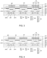
- FIG. 3 is a structural schematic view of a display panel provided by the third embodiment of the present disclosure.
- the display panel of this embodiment is the same as/similar to the display panel of the above-mentioned second embodiment, and the difference is that the linear polarizing layer described by this embodiment includes linear polarizing units 701 corresponding to the phase retardation units 601 and distributed in an array, and orthographic projections of the linear polarizing units 701 projected on the substrate 10 cover the orthographic projections of the phase retardation units 601 projected on the substrate 10.
- FIG. 4 is a structural schematic view of a display panel provided by the fourth embodiment of the present disclosure.
- the display panel of this embodiment is the same as/similar to the display panel of the above-mentioned third embodiment, and the difference is that the phase retardation units 601 and the linear polarizing units 701 in this embodiment are located between the inorganic layer 501 and the organic layer 502 which are adjacent to each other, the phase retardation layer (the phase retardation units 601) is made of the liquid crystal material, and alignment layers 90 are disposed on a surface of the phase retardation layer.
- the alignment layer 90 may be located on a side of the phase retardation unit 601 away from the linear polarizing unit 701 or on a side of the phase retardation unit 601 facing the linear polarizing unit 701, or the alignment layer 90 may be disposed on both sides of the phase retardation unit 601.
- a size of the alignment layers 90 may be adapted to a size of the phase retardation layer.
- the alignment layers 90 may be configured to be a whole layer, or may be distributed in an array.
- the phase retardation unit 601 and the linear polarizing unit 701 may be located on different film layers of the thin film encapsulation layer.
- the alignment layers 90 are used to align the liquid crystal material, thus causing a proper phase difference of the liquid crystal material, such as the phase difference of the quarter wavelength. Certainly, the liquid crystal material may be aligned according to actual requirements.
- the alignment layers 90 are disposed, so that the phase retardation units 601 causes different phase differences in this embodiment.
- the reflected light may be flexibly eliminated according to actual conditions.
- the anti-reflection (the elimination of the light) principle of the phase retardation units 601 and the linear polarizing units 701 in this embodiment is the same as the anti-reflection principle of the above-mentioned first embodiment, thus redundantly described in detail herein.
- the thickness of the display panel is greatly reduced by removing the conventional polarizer and disposing the phase retardation layer and the linear polarizing layer within the thin film encapsulation layer, thus improving the bending performance of the display panel.
- the combination of the phase retardation layer and the linear polarizing layer may effectively eliminate the reflected light caused by the external light irradiating the surface of the display panel.
- the reflected light caused by the external light irradiating the surface of the display panel may further be eliminated by disposing the black barrier walls with the light absorption function.
Landscapes
- Physics & Mathematics (AREA)
- Optics & Photonics (AREA)
- Chemical & Material Sciences (AREA)
- Engineering & Computer Science (AREA)
- Microelectronics & Electronic Packaging (AREA)
- Inorganic Chemistry (AREA)
- Crystallography & Structural Chemistry (AREA)
- General Physics & Mathematics (AREA)
- Electroluminescent Light Sources (AREA)
- Devices For Indicating Variable Information By Combining Individual Elements (AREA)
- Polarising Elements (AREA)
Abstract
Description
- The present disclosure relates to the field of display technology, and particularly, to a display panel.
- With development of technology and increase of people's requirement for products, flexible display screens have become a field that attracts much attention. Currently, reducing a thickness of the screen to achieve a foldable screen has become a development trend of future mobile screens. For conventional organic light-emitting diode (OLED) display screens, a polarizer of the OLED display screen is composed of a λ/4 phase retardation sheet and a linear polarizer, and the polarizer may effectively eliminate reflected light caused by external light irradiating a surface of the display screen. However, a thickness of the conventional polarizer is generally less than 100 µm, thereby limiting the thickness of the screen and reducing bending performance of the screen.
- Therefore, conventional technology has defects and requires to be solved urgently.
- The present disclosure provides a display panel to solve a problem in conventional display panels that disposition of a polarizer limits a thickness of the entire display panel and reduces bending performance of the display panel.
- In order to solve the above-mentioned problem, the present disclosure provides technical solutions as follows:
The present disclosure provides a display panel including: - a substrate;
- a thin film transistor array layer disposed on the substrate;
- a light emitting device layer disposed on the thin film transistor array layer;
- a thin film encapsulation layer disposed on the light emitting device layer;
- a phase retardation layer disposed within the thin film encapsulation layer; and
- a linear polarizing layer disposed within the thin film encapsulation layer.
- In the display panel of the present disclosure, the thin film encapsulation layer includes inorganic layers and an organic layer which are mutually stacked, and the phase retardation layer and the linear polarizing layer are located between the inorganic layer and the organic layer which are adjacent to each other, or the inorganic layer and/or the organic layer are disposed between the phase retardation layer and the linear polarizing layer.
- In the display panel of the present disclosure, the linear polarizing layer is located on a side of the phase retardation layer away from the light emitting device layer.
- In the display panel of the present disclosure, the light-emitting layer includes light emitting devices distributed in an array, the phase retardation layer includes phase retardation units corresponding to the light emitting devices and distributed in an array, and the display panel is provided with black barrier walls corresponding to gaps between the two adjacent phase retardation units.
- In the display panel of the present disclosure, the thin film transistor array layer includes an inorganic stacked layer and thin film transistors, the display panel is further provided with an organic stacked layer on the inorganic stacked layer, and the black barrier walls are located on the organic stacked layer or within the thin film encapsulation layer.
- In the display panel of the present disclosure, the linear polarizing layer includes linear polarizing units corresponding to the phase retardation units and distributed in an array, and orthographic projections of the linear polarizing units projected on the substrate cover orthographic projections of the phase retardation units projected on the substrate.
- In the display panel of the present disclosure, the phase retardation units cover a light emitting area of the light emitting device layer.
- In the display panel of the present disclosure, the phase retardation layer is made of an anisotropic organic material.
- In the display panel of the present disclosure, the phase retardation layer is made of a liquid crystal material, and alignment layers are disposed on a surface of the phase retardation layer.
- In the display panel of the present disclosure, a phase difference of the phase retardation layer is a quarter wavelength.
- In order to solve the above-mentioned problem, the present disclosure further provides a display panel including:
- a substrate;
- a thin film transistor array layer disposed on the substrate;
- a light emitting device layer disposed on the thin film transistor array layer;
- a thin film encapsulation layer disposed on the light emitting device layer;
- a phase retardation layer disposed within the thin film encapsulation layer; and
- a linear polarizing layer disposed within the thin film encapsulation layer, wherein the phase retardation layer and the linear polarizing layer are mutually stacked.
- In the display panel of the present disclosure, the thin film encapsulation layer includes inorganic layers and an organic layer which are mutually stacked, and the phase retardation layer and the linear polarizing layer are located between the inorganic layer and the organic layer which are adjacent to each other, or the inorganic layer and/or the organic layer are disposed between the phase retardation layer and the linear polarizing layer.
- In the display panel of the present disclosure, the linear polarizing layer is located on a side of the phase retardation layer away from the light emitting device layer.
- In the display panel of the present disclosure, the light-emitting layer includes light emitting devices distributed in an array, the phase retardation layer includes phase retardation units corresponding to the light emitting devices and distributed in an array, and the display panel is provided with black barrier walls corresponding to gaps between the two adjacent phase retardation units.
- In the display panel of the present disclosure, the thin film transistor array layer includes an inorganic stacked layer and thin film transistors, the display panel is further provided with an organic stacked layer on the inorganic stacked layer, and the black barrier walls are located on the organic stacked layer or within the thin film encapsulation layer.
- In the display panel of the present disclosure, the linear polarizing layer includes linear polarizing units corresponding to the phase retardation units and distributed in an array, and orthographic projections of the linear polarizing units projected on the substrate cover orthographic projections of the phase retardation units projected on the substrate.
- In the display panel of the present disclosure, the phase retardation units cover a light emitting area of the light emitting device layer.
- In the display panel of the present disclosure, the phase retardation layer is made of an anisotropic organic material.
- In the display panel of the present disclosure, the phase retardation layer is made of a liquid crystal material, and alignment layers are disposed on a surface of the phase retardation layer.
- In the display panel of the present disclosure, a phase difference of the phase retardation layer is a quarter wavelength.
- The advantageous effects of the present disclosure are that in comparison with the conventional display panels attached with the polarizers, a thickness of the display panel provides by the present disclosure is greatly reduced by removing the conventional polarizer and disposing the phase retardation layer and the linear polarizing layer within the thin film encapsulation layer, thus improving the bending performance of the display panel. Moreover, the combination of the phase retardation layer and the linear polarizing layer may effectively eliminate reflected light caused by external light irradiating a surface of the display panel.
- By illustrating specific implementations of the present disclosure in conjunction with accompanying drawings in detail below, technical solutions and other advantageous effects are obvious.
-
FIG. 1 is a structural schematic view of a display panel provided by a first embodiment of the present disclosure. -
FIG. 2 is a structural schematic view of a display panel provided by a second embodiment of the present disclosure. -
FIG. 3 is a structural schematic view of a display panel provided by a third embodiment of the present disclosure. -
FIG. 4 is a structural schematic view of a display panel provided by a fourth embodiment of the present disclosure. - In combination with accompanying drawings in embodiments of the present disclosure below, technical solutions in the embodiments of the present disclosure are clearly and completely described. Obviously, the described embodiments are merely a part of the embodiments of the present disclosure, rather than all the embodiments. Based on the embodiments in the present disclosure, all of other embodiments obtained by those skilled in the art without making for creative efforts belong to the scope protected by the present disclosure.
- In the description of the present disclosure, it should be understood that indicative directions or position relations, such as terms "longitudinal", "transverse", "length", "width", "upper", "lower", "front", "back", "left", "right", "vertical", and "horizontal", are based on directions or position relations indicated by the accompanying drawings. The indicative directions or position relations are only for convenience of describing the present disclosure and simplifying the description, and do not indicate or imply that indicated devices or elements must have a specific orientation and be constructed and operated in a specific orientation. Therefore, the indicative directions or position relations cannot be understood to be limitation to the present disclosure. In addition, terms, such as "first" and "second", are only used for purposes of description, and do not be understood to indicate or imply relative importance or to imply numbers of indicated technical features. Thus, the features defined with "first" and "second" may explicitly or implicitly include one or more of the features. In the description of the present disclosure, term "a plurality of" means two or more than two, unless specified otherwise. In the present disclosure, "/" means "or".
- Reference numerals and/or reference letters may be repeated in different examples in the present disclosure. This repeating is for the purposes of simplification and clarity, and does not refer to relations between various embodiments and/or settings.
- Referring to
FIG. 1 andFIG. 4 , the present disclosure provides a display panel including asubstrate 10 which may be a flexible substrate, but not limited to the flexible substrate, a thin filmtransistor array layer 20 disposed on thesubstrate 10, a light emittingdevice layer 40 disposed on the thin filmtransistor array layer 20, a thinfilm encapsulation layer 50 disposed on the light emittingdevice layer 40, a phase retardation layer 60 disposed within the thinfilm encapsulation layer 50, and a linearpolarizing layer 70 disposed within the thinfilm encapsulation layer 50, wherein the phase retardation layer 60 and the linearpolarizing layer 70 are mutually stacked. - The conventional organic light-emitting diode (OLED) display panels usually employ external polarizers. The polarizer generally is a composite film composed of a plurality of organic material layers including the λ/4 phase retardation layer and the linear polarizing layer, and these two birefringent layers may achieve an anti-reflection function of the screen. However, a plurality of thin films are required to protect and connect the λ/4 phase retardation layer with the linear polarizing layer, thus resulting in the polarizer with a great thickness. The thickness of the conventional polarizer is generally less than 100 µm, thereby limiting a thickness of the screen and reducing bending performance of the screen.
- In the display panel of the present disclosure, by removing the conventional polarizer and only disposing the phase retardation layer and the linear polarizing layer within the thin film encapsulation layer, the combination of the phase retardation layer and the linear polarizing layer may effectively eliminate reflected light caused by external light irradiating a surface of the display panel. In comparison with the conventional display panels attached with the polarizers, a thickness of the display panel of the present disclosure is greatly reduced, thereby improving the bending performance of the display panel and facilitating the development of the foldable display panels.
- In combination with the specific embodiments, the display panel described by the present disclosure is illustrated in detail below.
- Referring to
FIG. 1, FIG. 1 is a structural schematic view of a display panel provided by the first embodiment of the present disclosure. The thin filmtransistor array layer 20 is disposed on thesubstrate 10 and includes an inorganic stacked layer andthin film transistors 204. Specifically, the inorganic stacked layer includes, but is not limited to, a firstgate insulation layer 201, a secondgate insulation layer 202, and aninterlayer insulation layer 203 which are mutually stacked. Thethin film transistor 204 includes anactive layer 2041, agate electrode 2042, and a source/drain electrode 2043. Anelectrode layer 205 is disposed on thegate electrode 2042 and is insulated from thegate electrode 2042, and theelectrode layer 205 and thegate electrode 2042 form an electric capacity. - An organic stacked
layer 30 and the light emittingdevice layer 40 are also disposed on the inorganic stacked layer, and the organic stackedlayer 30 includes, but is not limited to, aplanarization layer 301 and apixel definition layer 302 which are mutually stacked. The light emittingdevice layer 40 includesanodes 401, light emittinglayers 402, acathode 403 which are mutually stacked. - The
anodes 401 are disposed on theplanarization layer 301, and are electrically connected to the source/drain electrodes 2043 of thethin film transistors 204 via through holes on theplanarization layer 301. Pixel holes are formed on sites of thepixel definition layer 302 corresponding to theanodes 401, thelight emitting layers 402 are located within the pixel holes, and thecathode 403 is disposed on the light emitting layers 402. - The thin
film encapsulation layer 50 is disposed on thecathode 403, and at least includes three laminated layers which are aninorganic layer 501, anorganic layer 502, and aninorganic layer 501. A thickness of the inorganic layer is generally in a range of several hundred nanometers, and a thickness of theorganic layer 502 is generally less than 20 µm. Theorganic layer 502 may not only be used to block water and oxygen but also function as a flat surface. - In order to reduce the thickness of the entire module of the display screen, the external polarizer is integrated into the thin
film encapsulation layer 50 of the display panel in the present disclosure. The thinfilm encapsulation layer 50 includes the phase retardation layer 60 and the linearpolarizing layer 70, and the linearpolarizing layer 70 is located on a side of the phase retardation layer 60 away from the light emittingdevice layer 40. - In the embodiment, the whole phase retardation layer 60 and the whole linear
polarizing layer 70 are disposed within the thinfilm encapsulation layer 50. Specifically, theinorganic layer 501 and/or theorganic layer 502 are disposed between the phase retardation layer 60 and the linearpolarizing layer 70, or the phase retardation layer 60 and the linearpolarizing layer 70 are located between the inorganic layer and the organic layer which are adjacent to each other. - In
FIG. 1 , the phase retardation layer 60 is located on a firstinorganic layer 501, theorganic layer 502 is disposed on the phase retardation layer 60, the linearpolarizing layer 70 is disposed on theorganic layer 502, and a secondinorganic layer 501 is disposed on the linearpolarizing layer 70. - In the embodiment, a phase difference of the phase retardation layer 60 is a quarter wavelength, and the phase retardation layer 60 may be a quarter wave plate.
- In the display panel of the embodiment, when the external incident light or nature light irradiates the surface of the display panel, the external incident light or nature light passes through the linear
polarizing layer 70 to be converted into linearly polarized light, such as the linearly polarized light in a horizontal direction, the linearly polarized light passed through the phase retardation layer 60 to be converted into circularly polarized light, and the circularly polarized light is reflected by thecathode 403 and theanodes 401, thus increasing the phase difference of π. For example, left-handed circularly polarized light is converted into right-handed circularly polarized light, or the right-handed circularly polarized light is converted into the left-handed circularly polarized light. The circularly polarized light with the phase retardation passes through the phase retardation layer 60 again to be converted into the linearly polarized light perpendicular to the incident linearly polarized light, such as the linearly polarized light in a vertical direction, so that the linearly polarized light in the vertical direction cannot pass through the linearpolarizing layer 70, thus achieving the elimination of the light. - Since the quarter wave plate of the conventional polarizer is mainly obtained by stretching polymer material, a thickness of the quarter wave plate generally requires to be several ten microns to reach a specific coefficient of the phase retardation. However, in the present disclosure, the phase retardation layer 60 may be made of a liquid crystal material or other anisotropic organic materials, and a thickness of the phase retardation layer 60 is in a range of one to several microns, thereby greatly reducing the thickness and improving the bending performance of the display panel.
- As shown in
FIG. 2, FIG. 2 is a structural schematic view of a display panel provided by the second embodiment of the present disclosure. The display panel of this embodiment is the same as/similar to the display panel of the above-mentioned first embodiment, and the difference is that the light emittingdevice layer 40 includes light emitting devices, i.e., pixels, distributed in an array, the phase retardation layer includesphase retardation units 601 corresponding to the light emitting devices and distributed in an array, and the display panel is provided withblack barrier walls 80 corresponding to gaps between the two adjacentphase retardation units 601. Theblack barrier walls 80 are made of a light absorbing material, and may effectively absorb the external incident light outside thephase retardation units 601. Therefore, the reflected light caused by the external light irradiating the surface of the display panel may be further eliminated. - The
black barrier walls 80 are located on the organic stackedlayer 30 or within the thinfilm encapsulation layer 50, and a height of theblack barrier walls 80 is in a range of several microns to several ten microns. - Specifically, the
black barrier walls 80 are located on thepixel definition layer 302, and may be configured to surround the pixel holes. Because of disposing theblack barrier walls 80, thecathode 403 and theinorganic layer 501 located on theblack barrier walls 80 may form recesses at sites corresponding to the pixel holes, and thephase retardation units 601 correspond to the recesses. - The
phase retardation units 601 cover a light emitting area of the light emittingdevice layer 40, and that is, orthographic projections of thephase retardation units 601 projected on thesubstrate 10 cover orthographic projections of thelight emitting layers 402 projected on thesubstrate 10. Thephase retardation units 601 may extend toward periphery of the pixel holes. - In an embodiment, the
black barrier walls 80 may be located on theinorganic layer 501 or theorganic layer 502 of the thinfilm encapsulation layer 50, and the external incident light outside thephase retardation units 601 may be absorbed by theblack barrier walls 80. - Specifically, the
black barrier walls 80 and thephase retardation units 601 may be located on the same layer, and the adjacentphase retardation units 601 may be separated by theblack barrier wall 80. - The anti-reflection (the elimination of the light) principle of the
phase retardation units 601 and the linearpolarizing layer 70 in this embodiment is the same as the anti-reflection principle of the above-mentioned first embodiment, and thus is not redundantly described in detail herein. - As shown in
FIG. 3, FIG. 3 is a structural schematic view of a display panel provided by the third embodiment of the present disclosure. The display panel of this embodiment is the same as/similar to the display panel of the above-mentioned second embodiment, and the difference is that the linear polarizing layer described by this embodiment includes linearpolarizing units 701 corresponding to thephase retardation units 601 and distributed in an array, and orthographic projections of the linearpolarizing units 701 projected on thesubstrate 10 cover the orthographic projections of thephase retardation units 601 projected on thesubstrate 10. - The advantageous effects of this embodiment are the same as the advantageous effects of the above-mentioned second embodiment, and the anti-reflection (the elimination of the light) principle of the
phase retardation units 601 and the linearpolarizing units 701 in this embodiment is the same as the anti-reflection principle of the above-mentioned first embodiment, and thus is not redundantly described in detail herein. - As shown in
FIG. 4, FIG. 4 is a structural schematic view of a display panel provided by the fourth embodiment of the present disclosure. The display panel of this embodiment is the same as/similar to the display panel of the above-mentioned third embodiment, and the difference is that thephase retardation units 601 and the linearpolarizing units 701 in this embodiment are located between theinorganic layer 501 and theorganic layer 502 which are adjacent to each other, the phase retardation layer (the phase retardation units 601) is made of the liquid crystal material, andalignment layers 90 are disposed on a surface of the phase retardation layer. - The
alignment layer 90 may be located on a side of thephase retardation unit 601 away from the linearpolarizing unit 701 or on a side of thephase retardation unit 601 facing the linearpolarizing unit 701, or thealignment layer 90 may be disposed on both sides of thephase retardation unit 601. - In an embodiment, a size of the alignment layers 90 may be adapted to a size of the phase retardation layer. The alignment layers 90 may be configured to be a whole layer, or may be distributed in an array. Certainly, the
phase retardation unit 601 and the linearpolarizing unit 701 may be located on different film layers of the thin film encapsulation layer. - The alignment layers 90 are used to align the liquid crystal material, thus causing a proper phase difference of the liquid crystal material, such as the phase difference of the quarter wavelength. Certainly, the liquid crystal material may be aligned according to actual requirements.
- In comparison with the above-mentioned third embodiment, the alignment layers 90 are disposed, so that the
phase retardation units 601 causes different phase differences in this embodiment. The reflected light may be flexibly eliminated according to actual conditions. - The anti-reflection (the elimination of the light) principle of the
phase retardation units 601 and the linearpolarizing units 701 in this embodiment is the same as the anti-reflection principle of the above-mentioned first embodiment, thus redundantly described in detail herein. - In comparison with the conventional display panels attached with the polarizers, the thickness of the display panel provides by the present disclosure is greatly reduced by removing the conventional polarizer and disposing the phase retardation layer and the linear polarizing layer within the thin film encapsulation layer, thus improving the bending performance of the display panel. Moreover, the combination of the phase retardation layer and the linear polarizing layer may effectively eliminate the reflected light caused by the external light irradiating the surface of the display panel. Additionally, the reflected light caused by the external light irradiating the surface of the display panel may further be eliminated by disposing the black barrier walls with the light absorption function.
- In summary, although the present disclosure has been disclosed by above preferred embodiments, the above preferred embodiments do not intend to limit the present disclosure, and those skilled in the art may make various changes and modifications without departing from the spirit and the scope of the present disclosure. Therefore, the protection scope of the present disclosure is defined by the scope of the claims.
Claims (20)
- A display panel, comprising:a substrate;a thin film transistor array layer disposed on the substrate;a light emitting device layer disposed on the thin film transistor array layer;a thin film encapsulation layer disposed on the light emitting device layer;a phase retardation layer disposed within the thin film encapsulation layer; anda linear polarizing layer disposed within the thin film encapsulation layer.
- The display panel according to claim 1, wherein the thin film encapsulation layer includes inorganic layers and an organic layer which are mutually stacked, and the phase retardation layer and the linear polarizing layer are located between the inorganic layer and the organic layer which are adjacent to each other, or the inorganic layer and/or the organic layer are disposed between the phase retardation layer and the linear polarizing layer.
- The display panel according to claim 2, wherein the linear polarizing layer is located on a side of the phase retardation layer away from the light emitting device layer.
- The display panel according to claim 1, wherein the light-emitting layer includes light emitting devices distributed in an array, the phase retardation layer includes phase retardation units corresponding to the light emitting devices and distributed in an array, and the display panel is provided with black barrier walls corresponding to gaps between the two adjacent phase retardation units.
- The display panel according to claim 4, wherein the thin film transistor array layer includes an inorganic stacked layer and thin film transistors, the display panel is further provided with an organic stacked layer on the inorganic stacked layer, and the black barrier walls are located on the organic stacked layer or within the thin film encapsulation layer.
- The display panel according to claim 4, wherein the linear polarizing layer includes linear polarizing units corresponding to the phase retardation units and distributed in an array, and orthographic projections of the linear polarizing units projected on the substrate cover orthographic projections of the phase retardation units projected on the substrate.
- The display panel according to claim 6, wherein the phase retardation units cover a light emitting area of the light emitting device layer.
- The display panel according to claim 1, wherein the phase retardation layer is made of an anisotropic organic material.
- The display panel according to claim 8, wherein the phase retardation layer is made of a liquid crystal material, and alignment layers are disposed on a surface of the phase retardation layer.
- The display panel according to claim 1, wherein a phase difference of the phase retardation layer is a quarter wavelength.
- A display panel, comprising:a substrate;a thin film transistor array layer disposed on the substrate;a light emitting device layer disposed on the thin film transistor array layer;a thin film encapsulation layer disposed on the light emitting device layer;a phase retardation layer disposed within the thin film encapsulation layer; anda linear polarizing layer disposed within the thin film encapsulation layer, wherein the phase retardation layer and the linear polarizing layer are mutually stacked.
- The display panel according to claim 11, wherein the thin film encapsulation layer includes inorganic layers and an organic layer which are mutually stacked, and the phase retardation layer and the linear polarizing layer are located between the inorganic layer and the organic layer which are adjacent to each other, or the inorganic layers and/or the organic layer are disposed between the phase retardation layer and the linear polarizing layer.
- The display panel according to claim 12, wherein the linear polarizing layer is located on a side of the phase retardation layer away from the light emitting device layer.
- The display panel according to claim 11, wherein the light-emitting layer includes light emitting devices distributed in an array, the phase retardation layer includes phase retardation units corresponding to the light emitting devices and distributed in an array, and the display panel is provided with black barrier walls corresponding to gaps between the two adjacent phase retardation units.
- The display panel according to claim 14, wherein the thin film transistor array layer includes an inorganic stacked layer and thin film transistors, the display panel is further provided with an organic stacked layer on the inorganic stacked layer, and the black barrier walls are located on the organic stacked layer or within the thin film encapsulation layer.
- The display panel according to claim 14, wherein the linear polarizing layer includes linear polarizing units corresponding to the phase retardation units and distributed in an array, and orthographic projections of the linear polarizing units projected on the substrate cover orthographic projections of the phase retardation units projected on the substrate.
- The display panel according to claim 16, wherein the phase retardation units cover a light emitting area of the light emitting device layer.
- The display panel according to claim 11, wherein the phase retardation layer is made of an anisotropic organic material.
- The display panel according to claim 18, wherein the phase retardation layer is made of a liquid crystal material, and alignment layers are disposed on a surface of the phase retardation layer.
- The display panel according to claim 11, wherein a phase difference of the phase retardation layer is a quarter wavelength.
Applications Claiming Priority (2)
| Application Number | Priority Date | Filing Date | Title |
|---|---|---|---|
| CN202010364425.6A CN111415975A (en) | 2020-04-30 | 2020-04-30 | a display panel |
| PCT/CN2020/095780 WO2021217800A1 (en) | 2020-04-30 | 2020-06-12 | Display panel |
Publications (2)
| Publication Number | Publication Date |
|---|---|
| EP4145524A1 true EP4145524A1 (en) | 2023-03-08 |
| EP4145524A4 EP4145524A4 (en) | 2024-05-29 |
Family
ID=71495109
Family Applications (1)
| Application Number | Title | Priority Date | Filing Date |
|---|---|---|---|
| EP20917292.3A Pending EP4145524A4 (en) | 2020-04-30 | 2020-06-12 | SCOREBOARD |
Country Status (6)
| Country | Link |
|---|---|
| US (1) | US11963393B2 (en) |
| EP (1) | EP4145524A4 (en) |
| JP (1) | JP2022534459A (en) |
| KR (1) | KR20210134887A (en) |
| CN (1) | CN111415975A (en) |
| WO (1) | WO2021217800A1 (en) |
Families Citing this family (10)
| Publication number | Priority date | Publication date | Assignee | Title |
|---|---|---|---|---|
| CN111799313B (en) * | 2020-07-17 | 2023-11-24 | 昆山工研院新型平板显示技术中心有限公司 | Display panel and display device |
| CN121865809A (en) * | 2020-09-02 | 2026-04-14 | 华为技术有限公司 | Combined film package in flexible display device and method of manufacturing the same |
| CN112071196A (en) * | 2020-09-08 | 2020-12-11 | 武汉华星光电半导体显示技术有限公司 | Display panel and display device |
| CN112420949A (en) * | 2020-11-17 | 2021-02-26 | 武汉华星光电半导体显示技术有限公司 | Display panel |
| CN112612373B (en) * | 2020-12-22 | 2023-04-28 | 湖北长江新型显示产业创新中心有限公司 | Display panel and display device |
| KR102766478B1 (en) * | 2021-01-28 | 2025-02-13 | 삼성디스플레이 주식회사 | Display apparatus and manufacturing the same |
| CN113113426A (en) | 2021-03-19 | 2021-07-13 | 武汉华星光电半导体显示技术有限公司 | Display panel and preparation method thereof |
| CN113471267B (en) * | 2021-06-30 | 2024-02-09 | 合肥维信诺科技有限公司 | Display panel |
| CN114335125B (en) * | 2021-12-30 | 2025-08-19 | 京东方科技集团股份有限公司 | Display substrate, preparation method thereof and display device |
| CN115799377A (en) * | 2022-11-07 | 2023-03-14 | 京东方科技集团股份有限公司 | Radiation detector panel and detection equipment |
Family Cites Families (23)
| Publication number | Priority date | Publication date | Assignee | Title |
|---|---|---|---|---|
| WO2004068182A2 (en) * | 2003-01-24 | 2004-08-12 | Digital Optics International Corporation | High density illumination system |
| KR20050018354A (en) * | 2003-08-12 | 2005-02-23 | 삼성전자주식회사 | Liquid crystal display, and manufacturing the same |
| WO2007063629A1 (en) * | 2005-12-02 | 2007-06-07 | Sharp Kabushiki Kaisha | Liquid crystal display device |
| KR20100063292A (en) * | 2008-12-03 | 2010-06-11 | 엘지디스플레이 주식회사 | Top emission type organic electro-luminescence device and method for fabricating of the same |
| KR101591332B1 (en) * | 2009-11-27 | 2016-02-03 | 엘지디스플레이 주식회사 | Organic electro-luminescence device |
| WO2011135638A1 (en) * | 2010-04-30 | 2011-11-03 | Iwata Shuji | Display element and display device |
| KR101754787B1 (en) * | 2011-05-23 | 2017-07-06 | 엘지디스플레이 주식회사 | Organic light emitting diodes and stereoscopic display device using the same |
| KR102110918B1 (en) * | 2013-10-29 | 2020-05-14 | 엘지디스플레이 주식회사 | Organic light emitting display, method of fabricating the same |
| JP2015128003A (en) * | 2013-12-27 | 2015-07-09 | ソニー株式会社 | Display device and electronic device |
| KR102440078B1 (en) * | 2015-03-10 | 2022-09-06 | 삼성디스플레이 주식회사 | Polarizing plate and display device including same |
| KR102403224B1 (en) * | 2015-04-03 | 2022-05-30 | 삼성디스플레이 주식회사 | Window and display device comprising the same |
| JP6784481B2 (en) * | 2015-07-13 | 2020-11-11 | 日東電工株式会社 | Circular polarizing plate for organic EL display device and organic EL display device |
| KR102703408B1 (en) * | 2016-06-10 | 2024-09-09 | 삼성디스플레이 주식회사 | Display device and fabricating method thereof |
| KR102608417B1 (en) * | 2016-08-19 | 2023-12-01 | 삼성디스플레이 주식회사 | Organic light emitting display device and method for manufacturing the same |
| KR102421594B1 (en) * | 2017-10-17 | 2022-07-15 | 삼성디스플레이 주식회사 | Display device |
| US10727279B2 (en) * | 2017-12-11 | 2020-07-28 | Lg Display Co., Ltd. | Organic light emitting diode display device |
| KR102569678B1 (en) * | 2017-12-26 | 2023-08-22 | 엘지디스플레이 주식회사 | Polarizing member and flexible display device including the same |
| CN109065579B (en) * | 2018-07-27 | 2021-03-19 | 广州国显科技有限公司 | Display panel, preparation method thereof and electronic equipment |
| KR102672451B1 (en) * | 2018-11-19 | 2024-06-04 | 엘지디스플레이 주식회사 | Organic light emitting diodes |
| WO2020261931A1 (en) * | 2019-06-27 | 2020-12-30 | 日本ゼオン株式会社 | Polarizing film and method for producing same, and display device |
| CN110289368B (en) * | 2019-06-27 | 2021-10-22 | 昆山工研院新型平板显示技术中心有限公司 | Display panel, display equipment and preparation method of display panel |
| CN110600514A (en) * | 2019-08-29 | 2019-12-20 | 武汉华星光电半导体显示技术有限公司 | Organic light emitting diode display panel and display device |
| CN111081747A (en) | 2019-12-25 | 2020-04-28 | 武汉华星光电半导体显示技术有限公司 | OLED display panel and preparation method thereof |
-
2020
- 2020-04-30 CN CN202010364425.6A patent/CN111415975A/en active Pending
- 2020-06-12 WO PCT/CN2020/095780 patent/WO2021217800A1/en not_active Ceased
- 2020-06-12 JP JP2021529023A patent/JP2022534459A/en active Pending
- 2020-06-12 KR KR1020217005320A patent/KR20210134887A/en not_active Ceased
- 2020-06-12 US US16/979,883 patent/US11963393B2/en active Active
- 2020-06-12 EP EP20917292.3A patent/EP4145524A4/en active Pending
Also Published As
| Publication number | Publication date |
|---|---|
| US11963393B2 (en) | 2024-04-16 |
| EP4145524A4 (en) | 2024-05-29 |
| WO2021217800A1 (en) | 2021-11-04 |
| KR20210134887A (en) | 2021-11-11 |
| JP2022534459A (en) | 2022-08-01 |
| CN111415975A (en) | 2020-07-14 |
| US20230096606A1 (en) | 2023-03-30 |
Similar Documents
| Publication | Publication Date | Title |
|---|---|---|
| US11963393B2 (en) | Display panel including phase retardation and linear polarizing layers | |
| US11335753B2 (en) | Display panel and display device having discontinuous organic light-emitting layer | |
| US20130032830A1 (en) | Organic light emitting display device and method of manufacturing the same | |
| CN110416273A (en) | Display panel and display device | |
| US10930892B1 (en) | OLED display panel having phase-compensated liquid crystal layer and manufacturing method thereof | |
| KR101094290B1 (en) | Organic light emitting display | |
| US11114646B2 (en) | Organic light emitting display panel and display device | |
| KR20170023231A (en) | Cover window for foldable display device and foldable display device including the same | |
| US10656460B2 (en) | Liquid crystal display and manufacturing method thereof | |
| JP7204550B2 (en) | Display device | |
| US10705636B2 (en) | Display panel and display device | |
| KR20060052259A (en) | Liquid crystal display | |
| KR101469482B1 (en) | Organic Emitting Display Device and Method of Manufacturing the same | |
| CN112909203B (en) | Display panel and display device | |
| KR20180069521A (en) | Cover window and Display device including the same | |
| CN115064559B (en) | Display panel and electronic device | |
| US11963428B2 (en) | Display panel and display device | |
| US11340493B2 (en) | Display device | |
| KR102467776B1 (en) | Display Device | |
| US20170250368A1 (en) | Display device | |
| US20240099111A1 (en) | Display substrate and method for manufacturing the same, display panel and display apparatus | |
| CN117334717A (en) | Display panels and display devices | |
| KR20130053976A (en) | Organic light emitting display device | |
| JP2018146824A (en) | Display device | |
| EP4339664B1 (en) | Display device |
Legal Events
| Date | Code | Title | Description |
|---|---|---|---|
| STAA | Information on the status of an ep patent application or granted ep patent |
Free format text: STATUS: UNKNOWN |
|
| STAA | Information on the status of an ep patent application or granted ep patent |
Free format text: STATUS: THE INTERNATIONAL PUBLICATION HAS BEEN MADE |
|
| PUAI | Public reference made under article 153(3) epc to a published international application that has entered the european phase |
Free format text: ORIGINAL CODE: 0009012 |
|
| STAA | Information on the status of an ep patent application or granted ep patent |
Free format text: STATUS: REQUEST FOR EXAMINATION WAS MADE |
|
| 17P | Request for examination filed |
Effective date: 20210813 |
|
| AK | Designated contracting states |
Kind code of ref document: A1 Designated state(s): AL AT BE BG CH CY CZ DE DK EE ES FI FR GB GR HR HU IE IS IT LI LT LU LV MC MK MT NL NO PL PT RO RS SE SI SK SM TR |
|
| RAP3 | Party data changed (applicant data changed or rights of an application transferred) |
Owner name: WUHAN CHINA STAR OPTOELECTRONICS SEMICONDUCTOR DISPLAY TECHNOLOGY CO., LTD. |
|
| DAV | Request for validation of the european patent (deleted) | ||
| DAX | Request for extension of the european patent (deleted) | ||
| REG | Reference to a national code |
Ref country code: DE Ref legal event code: R079 Free format text: PREVIOUS MAIN CLASS: H01L0027320000 Ipc: H10K0059120000 |
|
| A4 | Supplementary search report drawn up and despatched |
Effective date: 20240426 |
|
| RIC1 | Information provided on ipc code assigned before grant |
Ipc: H10K 59/80 20230101ALI20240422BHEP Ipc: H10K 59/12 20230101AFI20240422BHEP |