EP4145192A1 - Optical lens and camera module comprising same - Google Patents
Optical lens and camera module comprising same Download PDFInfo
- Publication number
- EP4145192A1 EP4145192A1 EP21797076.3A EP21797076A EP4145192A1 EP 4145192 A1 EP4145192 A1 EP 4145192A1 EP 21797076 A EP21797076 A EP 21797076A EP 4145192 A1 EP4145192 A1 EP 4145192A1
- Authority
- EP
- European Patent Office
- Prior art keywords
- optical lens
- area
- apodization
- lens according
- edge
- Prior art date
- Legal status (The legal status is an assumption and is not a legal conclusion. Google has not performed a legal analysis and makes no representation as to the accuracy of the status listed.)
- Pending
Links
Images



Classifications
-
- G—PHYSICS
- G02—OPTICS
- G02B—OPTICAL ELEMENTS, SYSTEMS OR APPARATUS
- G02B27/00—Optical systems or apparatus not provided for by any of the groups G02B1/00 - G02B26/00, G02B30/00
- G02B27/58—Optics for apodization or superresolution; Optical synthetic aperture systems
-
- G—PHYSICS
- G02—OPTICS
- G02B—OPTICAL ELEMENTS, SYSTEMS OR APPARATUS
- G02B27/00—Optical systems or apparatus not provided for by any of the groups G02B1/00 - G02B26/00, G02B30/00
- G02B27/0018—Optical systems or apparatus not provided for by any of the groups G02B1/00 - G02B26/00, G02B30/00 with means for preventing ghost images
-
- G—PHYSICS
- G02—OPTICS
- G02B—OPTICAL ELEMENTS, SYSTEMS OR APPARATUS
- G02B1/00—Optical elements characterised by the material of which they are made; Optical coatings for optical elements
- G02B1/10—Optical coatings produced by application to, or surface treatment of, optical elements
-
- G—PHYSICS
- G02—OPTICS
- G02B—OPTICAL ELEMENTS, SYSTEMS OR APPARATUS
- G02B13/00—Optical objectives specially designed for the purposes specified below
- G02B13/001—Miniaturised objectives for electronic devices, e.g. portable telephones, webcams, PDAs, small digital cameras
-
- G—PHYSICS
- G02—OPTICS
- G02B—OPTICAL ELEMENTS, SYSTEMS OR APPARATUS
- G02B30/00—Optical systems or apparatus for producing three-dimensional [3D] effects, e.g. stereoscopic images
-
- G—PHYSICS
- G02—OPTICS
- G02B—OPTICAL ELEMENTS, SYSTEMS OR APPARATUS
- G02B5/00—Optical elements other than lenses
- G02B5/003—Light absorbing elements
-
- G—PHYSICS
- G02—OPTICS
- G02B—OPTICAL ELEMENTS, SYSTEMS OR APPARATUS
- G02B5/00—Optical elements other than lenses
- G02B5/20—Filters
- G02B5/205—Neutral density filters
-
- G—PHYSICS
- G02—OPTICS
- G02B—OPTICAL ELEMENTS, SYSTEMS OR APPARATUS
- G02B7/00—Mountings, adjusting means, or light-tight connections, for optical elements
- G02B7/02—Mountings, adjusting means, or light-tight connections, for optical elements for lenses
-
- G—PHYSICS
- G03—PHOTOGRAPHY; CINEMATOGRAPHY; ANALOGOUS TECHNIQUES USING WAVES OTHER THAN OPTICAL WAVES; ELECTROGRAPHY; HOLOGRAPHY
- G03B—APPARATUS OR ARRANGEMENTS FOR TAKING PHOTOGRAPHS OR FOR PROJECTING OR VIEWING THEM; APPARATUS OR ARRANGEMENTS EMPLOYING ANALOGOUS TECHNIQUES USING WAVES OTHER THAN OPTICAL WAVES; ACCESSORIES THEREFOR
- G03B30/00—Camera modules comprising integrated lens units and imaging units, specially adapted for being embedded in other devices, e.g. mobile phones or vehicles
-
- G—PHYSICS
- G02—OPTICS
- G02B—OPTICAL ELEMENTS, SYSTEMS OR APPARATUS
- G02B3/00—Simple or compound lenses
- G02B2003/0093—Simple or compound lenses characterised by the shape
Definitions
- the present embodiment relates to an optical lens and a camera module comprising the same.
- the miniature camera includes a function of photographing a video as well as a digital image.
- the camera module comprises an image sensor, a lens barrel for accommodating a camera lens facing the image sensor, a voice coil motor (VCM) for narrowing or widening a gap between the camera lens and the image sensor, and an aperture.
- VCM voice coil motor
- a camera lens includes three or four optical lenses being overlappingly disposed.
- At least one of the optical lenses may be a D-cut lens having a straight part in which one side is cut out.
- FIG. 1 is a cross-sectional view of a D-cut lens according to the prior art
- FIG. 2 is a view illustrating an image measured through the D-cut lens of FIG. 1 .
- the D-cut lens 10 may have a straight part 12 of a shape in which one side is cut out.
- the D-cut lens 10 may include a plurality of mutually facing curved parts 14 and a plurality of mutually opposed straight parts 12.
- the straight part 12 may be formed by partially cutting out a circular lens.
- the above described D-cut lens may be applied to at least one optical lens among a plurality of optical lenses to reduce module height or Fno.
- the present embodiment is to provide an optical lens capable of reducing the occurrence of flare or ghost by improving the structure and a camera module comprising the same.
- an apodization area for reducing a flare phenomenon is disposed in an edge adjacent to the straight part of the optical lens.
- the apodization area may include a plurality of areas having different light transmittances.
- the apodization area may be formed to have a lower light transmittance as it travels toward an edge.
- the apodization area is an area coated with ink on the surface thereof, and the area coated may become thicker as it travels toward the edge.
- the apodization area is an area in which a plurality of patterns are disposed to be spaced apart from one another, and the cross-sectional shape of the pattern may include any one among a circular shape, an elliptical shape, and a polygonal shape.
- the pattern may be formed to have a larger size as it travels toward the edge.
- the gap between adjacent patterns may become closer as it travels toward the edge of the optical lens.
- the straight part is provided in plurality and disposed to face one another with respect to the center, and the curved part is provided in plurality and may be disposed to face one another with respect to the center.
- the linear distance between the plurality of straight parts is A and the thickness of the apodization area defined in a direction perpendicular to the straight part is C, it may be 0.05 ⁇ A ⁇ C ⁇ 0.5 ⁇ A .
- first, second, A, B, (a), and (b) may be used.
- a component when a component is described as being 'connected', 'coupled' or 'interconnected' to another component, the component is not only directly connected, coupled or interconnected to the other component, but may also include cases of being 'connected', 'coupled', or 'interconnected' due that another component between that other components.
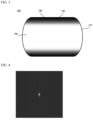
- FIG. 3 is a cross-sectional view of an optical lens according to an embodiment of the present invention
- FIG. 4 is a view illustrating an image measured through an optical lens according to an embodiment of the present invention
- FIG. 5 is a graph illustrating transmittance for each position of an optical lens according to an embodiment of the present invention
- FIG. 6 is an enlarged view of an apodization area in an optical lens according to an embodiment of the present invention.
- the optical lens 100 may be a D-cut lens.
- the optical lens 100 may include at least one curved part 110 and at least one straight part 120.
- the optical lens 100 may have a shape in which one side of a circular lens is cut out. The cut out area may form the straight part 120.
- the end portion of the curved part 110 may be formed in the shape of a curved line.
- the end portion of the straight part 120 may be formed in the shape of a straight line.
- the curved part 110 and the straight part 120 may be disposed in an edge area of the optical lens 110.
- a plurality of the curved part 110 may be disposed to face one another.
- the straight part 120 may be provided in plurality and disposed to face one another.
- the curved part 110 and the straight part 120 may be disposed adjacent to one another.
- the outer surface of the optical lens 110 may have a shape in which the curved part 110 and the straight part 120 are alternately disposed.
- the length of the straight part 120 may be formed to be longer than the length of the curved part 110. Unlike this, the length of the curved part 110 may be formed to be longer than the length of the straight part 120.
- the optical lens 110 may include an apodization area 140.
- the apodization area 140 may be formed on a surface of the optical lens 110.
- the apodization area 140 may be disposed on an incident surface or an exit surface of the optical lens 110.
- the apodization area 140 may be disposed at an edge of the optical lens 110.
- the apodization area 140 may be disposed in an edge area of the optical lens 110 adjacent to the straight part 120.
- the apodization area 140 may be disposed at an inner side of the straight part 120.
- the apodization area 140 may be provided in plurality so as to face one another with respect to the center of the optical lens 110.
- At least a portion of the apodization area 140 may be disposed at an inner side of the curved part 110. That is, the central portion of the apodization area 140 may be disposed at an inner side of the straight part 120, and both end portions may be disposed at an inner side of the curved part 110.
- the apodization area 140 may have a predetermined thickness with respect to the height of the optical lens 110.
- the height of the optical lens 110 may be defined as the length in an up and down direction between the plurality of straight parts 120.
- the apodization area 140 may include a plurality of areas having different light transmittances from one another.
- the apodization area 140 may be formed to have a lower light transmittance as it travels toward the edge of the optical lens 110.
- the apodization area 140 is a process for reducing a higher-order diffraction image, and a diffraction effect in the edge area of the optical lens 110 may be reduced.
- the apodization area 140 may be treated as a coating on a surface of the optical lens 110.
- the apodization area 140 may be an area coated with ink on a surface of the optical lens 110.
- the coating area may be formed to be thicker as it travels toward the edge of the optical lens 110.
- the apodization area 140 may be coated with a relatively darker ink as it travels toward the edge of the optical lens 110.
- the apodization area 140 may be implemented through a separate mechanism attached to a surface of the optical lens 110.
- the separate mechanism may include a spacer.
- a flare phenomenon due to a diffraction effect in an edge region of the optical lens 100 can be reduced.
- FIG. 7 is a view illustrating a modified embodiment of an apodization area according to an embodiment of the present invention.
- the apodization area 140 may be an area in which a plurality of patterns 180 is combined.
- the cross-sectional shape of the pattern 180 may include any one among a circular shape, an elliptical shape, and a polygonal shape.
- the pattern 180 may be formed to have a larger size as it travels toward the edge of the optical lens 100.
- a gap between adjacent patterns 180 may be formed to be closer as it travels toward the edge of the optical lens 100.
- FIGS. 8 to 12 are views for explaining light transmittance according to an arrangement structure of an apodization area inside an optical lens according to an embodiment of the present invention.
- the length of each area of the optical lens 100 may be defined as follows.
- the transmittance in the central area of the optical lens 100 excluding the apodization area 140 is 1, and assuming that the transmittance in areas other than the optical lens 100 is 0, as described above, it can be confirmed that the light transmittance is continuously decreased or increased in the apodization area 140.
- the thickness of the apodization area 140 satisfies the range of 0.05 ⁇ A ⁇ C ⁇ 0.5 ⁇ A . It can be confirmed that the flare phenomenon can be prevented and the brightness within the desired range can be obtained.
- the simulation result of the optical lens 100 according to the above-described range of C is as shown in FIG. 11 . That is, when the thickness of the apodization area 140 is increased more than necessary, the light transmittance of the optical lens 100 becomes very low, so the flare phenomenon prevention range in consideration of the light transmittance is the same as above.
- the linear distance A between the plurality of straight parts 120 and the maximum linear distance B between the plurality of curved parts 110 may satisfy the following relational expression.
- A ⁇ * B , 0.3 ⁇ ⁇ ⁇ 0.9
- ⁇ may be a D-cut ratio. That is, when ⁇ is within the above range compared to a circular lens, which is a normal lens, with the diameter of A, since the optical lens 100 has a satisfactory brightness ratio compared to the circular lens (refer to FIG. 12 ), the linear distance A between the plurality of straight parts 120 and the maximum linear distance B between the plurality of curved parts 110 may have the above relationship.
Landscapes
- Physics & Mathematics (AREA)
- General Physics & Mathematics (AREA)
- Optics & Photonics (AREA)
- Lenses (AREA)
- Lens Barrels (AREA)
Abstract
Description
- The present embodiment relates to an optical lens and a camera module comprising the same.
- Recently, a miniature camera has been widely used in portable devices, and the miniature camera includes a function of photographing a video as well as a digital image.
- The camera module comprises an image sensor, a lens barrel for accommodating a camera lens facing the image sensor, a voice coil motor (VCM) for narrowing or widening a gap between the camera lens and the image sensor, and an aperture.
- In general, a camera lens includes three or four optical lenses being overlappingly disposed.
- At least one of the optical lenses may be a D-cut lens having a straight part in which one side is cut out.
-
FIG. 1 is a cross-sectional view of a D-cut lens according to the prior art, andFIG. 2 is a view illustrating an image measured through the D-cut lens ofFIG. 1 . - Referring to
FIGS. 1 and 2 , the D-cutlens 10 according to the prior art may have astraight part 12 of a shape in which one side is cut out. For example, the D-cutlens 10 may include a plurality of mutually facingcurved parts 14 and a plurality of mutually opposedstraight parts 12. Thestraight part 12 may be formed by partially cutting out a circular lens. - In a camera module to which a prism or mirror is applied, the above described D-cut lens may be applied to at least one optical lens among a plurality of optical lenses to reduce module height or Fno.
- However, as illustrated in
FIG. 2 , due to the shape of the D-cut lens itself, there is a problem in that a flare phenomenon or a ghost occurs when light is reflected through the D-cut lens. - The present embodiment is to provide an optical lens capable of reducing the occurrence of flare or ghost by improving the structure and a camera module comprising the same.
- As an embodiment, in an optical lens including at least one straight part and a curved part on an outer surface thereof, an apodization area for reducing a flare phenomenon is disposed in an edge adjacent to the straight part of the optical lens.
- The apodization area may include a plurality of areas having different light transmittances.
- The apodization area may be formed to have a lower light transmittance as it travels toward an edge.
- The apodization area is an area coated with ink on the surface thereof, and the area coated may become thicker as it travels toward the edge.
- The apodization area is an area in which a plurality of patterns are disposed to be spaced apart from one another, and the cross-sectional shape of the pattern may include any one among a circular shape, an elliptical shape, and a polygonal shape.
- The pattern may be formed to have a larger size as it travels toward the edge.
- The gap between adjacent patterns may become closer as it travels toward the edge of the optical lens.
- The straight part is provided in plurality and disposed to face one another with respect to the center, and the curved part is provided in plurality and may be disposed to face one another with respect to the center.
- Assuming that the linear distance between the plurality of straight parts is A and the thickness of the apodization area defined in a direction perpendicular to the straight part is C, it may be 0.05∗ A ≤ C ≤ 0.5∗ A.
- Assuming that the linear distance between the plurality of straight parts is A, and the maximum linear distance B between the plurality of curved parts is B, it may be A=α∗ B, (0.3 ≤ α ≤ 0.9).
- Through the present embodiment, there is an advantage in that the flare and ghost phenomena can be reduced due to the diffraction effect of the apodization area in an edge area of the optical lens.
-
-
FIG. 1 is a cross-sectional view of a D-cut lens according to the prior art. -
FIG. 2 is a view illustrating an image being measured through the D-cut lens ofFIG. 1 . -
FIG. 3 is a cross-sectional view of an optical lens according to an embodiment of the present invention; -
FIG. 4 is a view illustrating an image measured through an optical lens according to an embodiment of the present invention. -
FIG. 5 is a graph illustrating transmittance for each position of an optical lens according to an embodiment of the present invention. -
FIG. 6 is an enlarged view of an apodization area in an optical lens according to an embodiment of the present invention. -
FIG. 7 is a view illustrating a modified embodiment of an apodization area according to an embodiment of the present invention. -
FIGS. 8 to 12 are diagrams for explaining light transmittance according to an arrangement structure of an apodization area in an optical lens according to an embodiment of the present invention. - Hereinafter, preferred embodiments of the present invention will be described in detail with reference to the accompanying drawings.
- However, the technical idea of the present invention is not limited to some embodiments to be described, but may be implemented in various forms, and within the scope of the technical idea of the present invention, one or more of the constituent elements may be selectively combined or substituted between embodiments.
- In addition, the terms (including technical and scientific terms) used in the embodiments of the present invention, unless explicitly defined and described, can be interpreted as a meaning that can be generally understood by a person skilled in the art, and commonly used terms such as terms defined in the dictionary may be interpreted in consideration of the meaning of the context of the related technology.
- In addition, terms used in the present specification are for describing embodiments and are not intended to limit the present invention. In the present specification, the singular form may include the plural form unless specifically stated in the phrase, and when described as "at least one (or more than one) of A and B and C", it may include one or more of all combinations that can be combined with A, B, and C.
- In addition, in describing the components of the embodiment of the present invention, terms such as first, second, A, B, (a), and (b) may be used.
- These terms are merely intended to distinguish the components from other components, and the terms do not limit the nature, order or sequence of the components.
- And, when a component is described as being 'connected', 'coupled' or 'interconnected' to another component, the component is not only directly connected, coupled or interconnected to the other component, but may also include cases of being 'connected', 'coupled', or 'interconnected' due that another component between that other components.
- In addition, when described as being formed or arranged in "on (above)" or "below (under)" of each component, "on (above)" or "below (under)" means that it includes not only the case where the two components are directly in contact with, but also the case where one or more other components are formed or arranged between the two components. In addition, when expressed as "on (above)" or "below (under)", the meaning of not only an upward direction but also a downward direction based on one component may be included.
-
FIG. 3 is a cross-sectional view of an optical lens according to an embodiment of the present invention;FIG. 4 is a view illustrating an image measured through an optical lens according to an embodiment of the present invention;FIG. 5 is a graph illustrating transmittance for each position of an optical lens according to an embodiment of the present invention; andFIG. 6 is an enlarged view of an apodization area in an optical lens according to an embodiment of the present invention. - Referring to
FIGS. 3 to 5 , theoptical lens 100 according to an embodiment of the present invention may be a D-cut lens. Theoptical lens 100 may include at least onecurved part 110 and at least onestraight part 120. Theoptical lens 100 may have a shape in which one side of a circular lens is cut out. The cut out area may form thestraight part 120. - The end portion of the
curved part 110 may be formed in the shape of a curved line. The end portion of thestraight part 120 may be formed in the shape of a straight line. Thecurved part 110 and thestraight part 120 may be disposed in an edge area of theoptical lens 110. A plurality of thecurved part 110 may be disposed to face one another. Thestraight part 120 may be provided in plurality and disposed to face one another. Thecurved part 110 and thestraight part 120 may be disposed adjacent to one another. The outer surface of theoptical lens 110 may have a shape in which thecurved part 110 and thestraight part 120 are alternately disposed. - The length of the
straight part 120 may be formed to be longer than the length of thecurved part 110. Unlike this, the length of thecurved part 110 may be formed to be longer than the length of thestraight part 120. - The
optical lens 110 may include anapodization area 140. Theapodization area 140 may be formed on a surface of theoptical lens 110. Theapodization area 140 may be disposed on an incident surface or an exit surface of theoptical lens 110. Theapodization area 140 may be disposed at an edge of theoptical lens 110. - The
apodization area 140 may be disposed in an edge area of theoptical lens 110 adjacent to thestraight part 120. Theapodization area 140 may be disposed at an inner side of thestraight part 120. When thestraight part 120 is provided in plurality, theapodization area 140 may be provided in plurality so as to face one another with respect to the center of theoptical lens 110. - In some cases, at least a portion of the
apodization area 140 may be disposed at an inner side of thecurved part 110. That is, the central portion of theapodization area 140 may be disposed at an inner side of thestraight part 120, and both end portions may be disposed at an inner side of thecurved part 110. - The
apodization area 140 may have a predetermined thickness with respect to the height of theoptical lens 110. Here, the height of theoptical lens 110 may be defined as the length in an up and down direction between the plurality ofstraight parts 120. - As illustrated in
FIG. 6 , theapodization area 140 may include a plurality of areas having different light transmittances from one another. Theapodization area 140 may be formed to have a lower light transmittance as it travels toward the edge of theoptical lens 110. - The
apodization area 140 is a process for reducing a higher-order diffraction image, and a diffraction effect in the edge area of theoptical lens 110 may be reduced. Theapodization area 140 may be treated as a coating on a surface of theoptical lens 110. Theapodization area 140 may be an area coated with ink on a surface of theoptical lens 110. To form anapodization area 140 as shown inFIG. 6 , the coating area may be formed to be thicker as it travels toward the edge of theoptical lens 110. In addition, theapodization area 140 may be coated with a relatively darker ink as it travels toward the edge of theoptical lens 110. - Meanwhile, the
apodization area 140 may be implemented through a separate mechanism attached to a surface of theoptical lens 110. For example, the separate mechanism may include a spacer. - According to the above structure, as illustrated in
FIG. 4 , a flare phenomenon due to a diffraction effect in an edge region of theoptical lens 100 can be reduced. - In addition, as illustrated in
FIG. 5 , it is possible to prevent abrupt change in the light transmittance in an edge area (an area where thestraight part 120 is disposed) of theoptical lens 100. In other words, since the airy disk size of theoptical lens 100 is reduced due to theapodization area 140, the diffraction effect may also be reduced. -
FIG. 7 is a view illustrating a modified embodiment of an apodization area according to an embodiment of the present invention. - Referring to
FIG. 7 , theapodization area 140 may be an area in which a plurality ofpatterns 180 is combined. The cross-sectional shape of thepattern 180 may include any one among a circular shape, an elliptical shape, and a polygonal shape. Thepattern 180 may be formed to have a larger size as it travels toward the edge of theoptical lens 100. In addition, a gap betweenadjacent patterns 180 may be formed to be closer as it travels toward the edge of theoptical lens 100. -
FIGS. 8 to 12 are views for explaining light transmittance according to an arrangement structure of an apodization area inside an optical lens according to an embodiment of the present invention. - Referring to
FIG. 8 , the length of each area of theoptical lens 100 may be defined as follows. - A: The linear distance between a plurality of straight parts 120 (size of optical lens)
- B: The maximum linear distance between a plurality of the curved parts 110 (effective diameter of optical lens)
- C: The thickness of the
apodization area 140 measured in a direction perpendicular to thestraight part 120 - Referring to
FIG. 9 , assuming that the transmittance in the central area of theoptical lens 100 excluding theapodization area 140 is 1, and assuming that the transmittance in areas other than theoptical lens 100 is 0, as described above, it can be confirmed that the light transmittance is continuously decreased or increased in theapodization area 140. - In addition, referring to the graph of
FIG. 10 illustrating the brightness ratio of theoptical lens 100 according to the size of C, when the thickness of theapodization area 140 satisfies the range of 0.05∗ A ≤ C ≤ 0.5∗ A, it can be confirmed that the flare phenomenon can be prevented and the brightness within the desired range can be obtained. The simulation result of theoptical lens 100 according to the above-described range of C is as shown inFIG. 11 . That is, when the thickness of theapodization area 140 is increased more than necessary, the light transmittance of theoptical lens 100 becomes very low, so the flare phenomenon prevention range in consideration of the light transmittance is the same as above. - In addition, the linear distance A between the plurality of
straight parts 120 and the maximum linear distance B between the plurality ofcurved parts 110 may satisfy the following relational expression.
optical lens 100 has a satisfactory brightness ratio compared to the circular lens (refer toFIG. 12 ), the linear distance A between the plurality ofstraight parts 120 and the maximum linear distance B between the plurality ofcurved parts 110 may have the above relationship. - In the above description, it is described that all the components constituting the embodiments of the present invention are combined or operated in one, but the present invention is not necessarily limited to these embodiments. In other words, within the scope of the present invention, all of the components may be selectively operated in combination with one or more. In addition, the terms "comprise", "include" or "having" described above mean that the corresponding component may be inherent unless specifically stated otherwise, and thus it should be construed that it does not exclude other components, but further include other components instead. All terms, including technical and scientific terms, have the same meaning as commonly understood by one of ordinary skill in the art unless otherwise defined. Terms used generally, such as terms defined in a dictionary, should be interpreted to coincide with the contextual meaning of the related art, and shall not be interpreted in an ideal or excessively formal sense unless explicitly defined in the present invention.
- The above description is merely illustrative of the technical idea of the present invention, and those skilled in the art to which the present invention pertains may make various modifications and changes without departing from the essential characteristics of the present invention. Therefore, the embodiments disclosed in the present invention are not intended to limit the technical idea of the present invention but to describe the present invention, and the scope of the technical idea of the present invention is not limited by these embodiments. The protection scope of the present invention should be interpreted by the following claims, and all technical ideas within the equivalent scope should be interpreted as being included in the scope of the present invention.
Claims (10)
- An optical lens comprising at least one straight part and at least one curved part on an outer surface thereof,
wherein an apodization area for reducing a flare phenomenon is disposed at an edge adjacent to the straight part. - The optical lens according to claim 1,
wherein the apodization area includes a plurality of areas having different light transmittances from one another. - The optical lens according to claim 2,
wherein the apodization area is formed to have a lower light transmittance as it travels toward an edge. - The optical lens according to claim 1,wherein the apodization area is an area coated with ink on the surface thereof, andwherein the area coated becomes thicker as it travels toward the edge.
- The optical lens according to claim 1,wherein the apodization area is an area in which a plurality of patterns are disposed to be spaced apart from one another, andwherein the cross-sectional shape of the pattern includes any one among a circular shape, an elliptical shape, and a polygonal shape.
- The optical lens according to claim 1,
wherein the pattern is formed to have a larger size as it travels toward the edge. - The optical lens according to claim 5,
wherein the gap between adjacent patterns becomes closer as it travels toward the edge of the optical lens. - The optical lens according to claim 1,wherein the straight part is provided in plurality and disposed to face one another with respect to the center, andwherein the curved part is provided in plurality and is disposed to face one another with respect to the center.
- The optical lens according to claim 8,
wherein when the linear distance between the plurality of straight parts is A and the thickness of the apodization area defined in a direction perpendicular to the straight part is C,
- The optical lens according to claim 8,
wherein when the linear distance between the plurality of straight parts is A and the maximum linear distance B between the plurality of curved parts is B,
Applications Claiming Priority (2)
| Application Number | Priority Date | Filing Date | Title |
|---|---|---|---|
| KR1020200052941A KR102954563B1 (en) | 2020-04-29 | LED Light source module | |
| PCT/KR2021/005482 WO2021221483A1 (en) | 2020-04-29 | 2021-04-29 | Optical lens and camera module comprising same |
Publications (2)
| Publication Number | Publication Date |
|---|---|
| EP4145192A1 true EP4145192A1 (en) | 2023-03-08 |
| EP4145192A4 EP4145192A4 (en) | 2024-05-15 |
Family
ID=78373716
Family Applications (1)
| Application Number | Title | Priority Date | Filing Date |
|---|---|---|---|
| EP21797076.3A Pending EP4145192A4 (en) | 2020-04-29 | 2021-04-29 | OPTICAL LENS AND CAMERA MODULE |
Country Status (5)
| Country | Link |
|---|---|
| US (1) | US12517349B2 (en) |
| EP (1) | EP4145192A4 (en) |
| JP (1) | JP7798792B2 (en) |
| CN (1) | CN115461655A (en) |
| WO (1) | WO2021221483A1 (en) |
Family Cites Families (19)
| Publication number | Priority date | Publication date | Assignee | Title |
|---|---|---|---|---|
| US5541779A (en) | 1993-11-17 | 1996-07-30 | Daewoo Electronics Co., Ltd. | Optical imaging system |
| JP3457372B2 (en) * | 1993-12-28 | 2003-10-14 | 日本写真印刷株式会社 | Lens with aperture function and method of manufacturing the same |
| JP2005266096A (en) * | 2004-03-17 | 2005-09-29 | Canon Inc | Optical filter and photographing apparatus |
| JP2006145831A (en) * | 2004-11-19 | 2006-06-08 | Casio Comput Co Ltd | Optical lens |
| JP2006267391A (en) * | 2005-03-23 | 2006-10-05 | Mitsubishi Electric Corp | Imaging device |
| US20070139792A1 (en) * | 2005-12-21 | 2007-06-21 | Michel Sayag | Adjustable apodized lens aperture |
| KR100951187B1 (en) | 2008-06-26 | 2010-04-06 | 삼성전기주식회사 | Camera module |
| JP5469944B2 (en) | 2009-07-17 | 2014-04-16 | 株式会社シグマ | Imaging device |
| JP2011043679A (en) | 2009-08-21 | 2011-03-03 | Fujifilm Corp | Zoom lens and image pickup apparatus |
| JP5452329B2 (en) | 2010-04-06 | 2014-03-26 | 富士フイルム株式会社 | Filter, imaging lens, imaging device, and portable terminal device |
| JP2014211617A (en) | 2013-04-01 | 2014-11-13 | 株式会社コシナ | Apodization filter, and manufacturing method thereof |
| JP2015094911A (en) * | 2013-11-14 | 2015-05-18 | パナソニック株式会社 | Manufacturing method of optical lens having apodization function |
| WO2016039147A1 (en) | 2014-09-11 | 2016-03-17 | 富士フイルム株式会社 | Lens barrel, imaging device main body, and imaging device |
| TWI537628B (en) | 2014-11-12 | 2016-06-11 | 台灣東電化股份有限公司 | Slimed lens module |
| JP6289526B2 (en) | 2016-03-03 | 2018-03-07 | キヤノン株式会社 | Optical element and optical system having the same |
| US10473880B2 (en) | 2017-12-12 | 2019-11-12 | Samsung Electro-Mechanics Co., Ltd. | Portable electronic device, camera module, and lens assembly |
| KR102108199B1 (en) | 2017-12-12 | 2020-05-08 | 삼성전기주식회사 | Lens assembly and camera module including the same |
| US11048067B2 (en) * | 2018-05-25 | 2021-06-29 | Anteryon International B.V. | Lens system |
| CN113960757B (en) * | 2021-11-02 | 2023-07-04 | 江西晶超光学有限公司 | Optical lens, camera module and electronic equipment |
-
2021
- 2021-04-29 JP JP2022566188A patent/JP7798792B2/en active Active
- 2021-04-29 EP EP21797076.3A patent/EP4145192A4/en active Pending
- 2021-04-29 WO PCT/KR2021/005482 patent/WO2021221483A1/en not_active Ceased
- 2021-04-29 CN CN202180031793.1A patent/CN115461655A/en active Pending
- 2021-04-29 US US17/997,314 patent/US12517349B2/en active Active
Also Published As
| Publication number | Publication date |
|---|---|
| EP4145192A4 (en) | 2024-05-15 |
| JP2023524471A (en) | 2023-06-12 |
| US20230168492A1 (en) | 2023-06-01 |
| WO2021221483A1 (en) | 2021-11-04 |
| US12517349B2 (en) | 2026-01-06 |
| CN115461655A (en) | 2022-12-09 |
| KR20210133813A (en) | 2021-11-08 |
| JP7798792B2 (en) | 2026-01-14 |
Similar Documents
| Publication | Publication Date | Title |
|---|---|---|
| US20230078102A1 (en) | Optical imaging lens | |
| JP3584107B2 (en) | Zoom lens | |
| JP5345008B2 (en) | Projection variable focus lens and projection display device | |
| JP3652046B2 (en) | Compact zoom optical system and camera equipped with the same | |
| US20080285142A1 (en) | Projection zoom lens | |
| JP3599689B2 (en) | Zoom lens | |
| US20210132334A1 (en) | Optical imaging lens | |
| CN111929815A (en) | Optical imaging lens | |
| JPH10104520A (en) | Wide-angle zoom lens | |
| JP5320224B2 (en) | Projection variable focus lens and projection display device | |
| US9030754B2 (en) | Zoom lens | |
| US8922698B2 (en) | Image pickup apparatus with removable ND filter | |
| CN111650726B (en) | Optical imaging lens | |
| JPH09218348A (en) | Photographic lens | |
| JP3352264B2 (en) | Retrofocus type lens and camera having the same | |
| JPH1031155A (en) | Zoom lens | |
| US7038857B1 (en) | Projection zoom lens | |
| EP4145192A1 (en) | Optical lens and camera module comprising same | |
| JPH04362909A (en) | Zoom lens with anti-shake optical system | |
| US6437923B1 (en) | High zoom ratio lens | |
| US20250102765A1 (en) | Optical imaging lens | |
| US9028078B2 (en) | Lens apparatus and image pickup apparatus including the same | |
| JPH07174972A (en) | Variable power lens for copying | |
| US12196925B2 (en) | Optical imaging lens | |
| US6577452B2 (en) | Variable focal length lens system |
Legal Events
| Date | Code | Title | Description |
|---|---|---|---|
| STAA | Information on the status of an ep patent application or granted ep patent |
Free format text: STATUS: THE INTERNATIONAL PUBLICATION HAS BEEN MADE |
|
| PUAI | Public reference made under article 153(3) epc to a published international application that has entered the european phase |
Free format text: ORIGINAL CODE: 0009012 |
|
| STAA | Information on the status of an ep patent application or granted ep patent |
Free format text: STATUS: REQUEST FOR EXAMINATION WAS MADE |
|
| 17P | Request for examination filed |
Effective date: 20221026 |
|
| AK | Designated contracting states |
Kind code of ref document: A1 Designated state(s): AL AT BE BG CH CY CZ DE DK EE ES FI FR GB GR HR HU IE IS IT LI LT LU LV MC MK MT NL NO PL PT RO RS SE SI SK SM TR |
|
| DAV | Request for validation of the european patent (deleted) | ||
| DAX | Request for extension of the european patent (deleted) | ||
| REG | Reference to a national code |
Ref country code: DE Ref legal event code: R079 Free format text: PREVIOUS MAIN CLASS: G02B0005180000 Ipc: G02B0027000000 |
|
| A4 | Supplementary search report drawn up and despatched |
Effective date: 20240412 |
|
| RIC1 | Information provided on ipc code assigned before grant |
Ipc: G02B 3/00 20060101ALN20240408BHEP Ipc: G02B 27/58 20060101ALI20240408BHEP Ipc: G02B 5/20 20060101ALI20240408BHEP Ipc: G03B 30/00 20210101ALI20240408BHEP Ipc: G02B 13/00 20060101ALI20240408BHEP Ipc: G02B 5/00 20060101ALI20240408BHEP Ipc: G02B 1/10 20150101ALI20240408BHEP Ipc: G02B 27/00 20060101AFI20240408BHEP |