EP4143961B1 - Drive device, optical system and lithography apparatus - Google Patents
Drive device, optical system and lithography apparatus Download PDFInfo
- Publication number
- EP4143961B1 EP4143961B1 EP21722389.0A EP21722389A EP4143961B1 EP 4143961 B1 EP4143961 B1 EP 4143961B1 EP 21722389 A EP21722389 A EP 21722389A EP 4143961 B1 EP4143961 B1 EP 4143961B1
- Authority
- EP
- European Patent Office
- Prior art keywords
- actuator
- signal
- voltage
- drive device
- drive
- Prior art date
- Legal status (The legal status is an assumption and is not a legal conclusion. Google has not performed a legal analysis and makes no representation as to the accuracy of the status listed.)
- Active
Links
Images





Classifications
-
- G—PHYSICS
- G02—OPTICS
- G02B—OPTICAL ELEMENTS, SYSTEMS OR APPARATUS
- G02B26/00—Optical devices or arrangements for the control of light using movable or deformable optical elements
- G02B26/08—Optical devices or arrangements for the control of light using movable or deformable optical elements for controlling the direction of light
- G02B26/0816—Optical devices or arrangements for the control of light using movable or deformable optical elements for controlling the direction of light by means of one or more reflecting elements
- G02B26/0833—Optical devices or arrangements for the control of light using movable or deformable optical elements for controlling the direction of light by means of one or more reflecting elements the reflecting element being a micromechanical device, e.g. a MEMS mirror, DMD
-
- G—PHYSICS
- G02—OPTICS
- G02B—OPTICAL ELEMENTS, SYSTEMS OR APPARATUS
- G02B5/00—Optical elements other than lenses
- G02B5/08—Mirrors
- G02B5/09—Multifaceted or polygonal mirrors, e.g. polygonal scanning mirrors; Fresnel mirrors
-
- G—PHYSICS
- G02—OPTICS
- G02B—OPTICAL ELEMENTS, SYSTEMS OR APPARATUS
- G02B7/00—Mountings, adjusting means, or light-tight connections, for optical elements
- G02B7/18—Mountings, adjusting means, or light-tight connections, for optical elements for prisms; for mirrors
- G02B7/182—Mountings, adjusting means, or light-tight connections, for optical elements for prisms; for mirrors for mirrors
-
- G—PHYSICS
- G03—PHOTOGRAPHY; CINEMATOGRAPHY; ANALOGOUS TECHNIQUES USING WAVES OTHER THAN OPTICAL WAVES; ELECTROGRAPHY; HOLOGRAPHY
- G03F—PHOTOMECHANICAL PRODUCTION OF TEXTURED OR PATTERNED SURFACES, e.g. FOR PRINTING, FOR PROCESSING OF SEMICONDUCTOR DEVICES; MATERIALS THEREFOR; ORIGINALS THEREFOR; APPARATUS SPECIALLY ADAPTED THEREFOR
- G03F7/00—Photomechanical, e.g. photolithographic, production of textured or patterned surfaces, e.g. printing surfaces; Materials therefor, e.g. comprising photoresists; Apparatus specially adapted therefor
- G03F7/70—Microphotolithographic exposure; Apparatus therefor
- G03F7/70216—Mask projection systems
- G03F7/70258—Projection system adjustments, e.g. adjustments during exposure or alignment during assembly of projection system
- G03F7/70266—Adaptive optics, e.g. deformable optical elements for wavefront control, e.g. for aberration adjustment or correction
-
- H—ELECTRICITY
- H02—GENERATION; CONVERSION OR DISTRIBUTION OF ELECTRIC POWER
- H02N—ELECTRIC MACHINES NOT OTHERWISE PROVIDED FOR
- H02N2/00—Electric machines in general using piezoelectric effect, electrostriction or magnetostriction
- H02N2/0005—Electric machines in general using piezoelectric effect, electrostriction or magnetostriction producing non-specific motion; Details common to machines covered by H02N2/02 - H02N2/16
- H02N2/0075—Electrical details, e.g. drive or control circuits or methods
-
- H—ELECTRICITY
- H02—GENERATION; CONVERSION OR DISTRIBUTION OF ELECTRIC POWER
- H02N—ELECTRIC MACHINES NOT OTHERWISE PROVIDED FOR
- H02N2/00—Electric machines in general using piezoelectric effect, electrostriction or magnetostriction
- H02N2/02—Electric machines in general using piezoelectric effect, electrostriction or magnetostriction producing linear motion, e.g. actuators; Linear positioners ; Linear motors
- H02N2/06—Drive circuits; Control arrangements or methods
- H02N2/062—Small signal circuits; Means for controlling position or derived quantities, e.g. for removing hysteresis
-
- G—PHYSICS
- G02—OPTICS
- G02B—OPTICAL ELEMENTS, SYSTEMS OR APPARATUS
- G02B5/00—Optical elements other than lenses
- G02B5/08—Mirrors
- G02B5/0891—Ultraviolet [UV] mirrors
Definitions
- the present invention relates to a drive device for driving an actuator of an optical system, to an optical system comprising such a drive device, and to a lithography apparatus comprising such an optical system.
- Microlithography apparatuses which have actuatable optical elements, such as, for example, microlens element arrays or micromirror arrays.
- Microlithography is used for producing microstructured components, such as, for example, integrated circuits.
- the microlithography process is performed using a lithography apparatus, which has an illumination system and a projection system.
- the image of a mask (reticle) illuminated by means of the illumination system is in this case projected by means of the projection system onto a substrate, for example a silicon wafer, which is coated with a light-sensitive layer (photoresist) and arranged in the image plane of the projection system, in order to transfer the mask structure to the light-sensitive coating of the substrate.
- the imaging of the mask on the substrate can be improved by means of actuatable optical elements.
- wavefront aberrations during exposure which result in magnified and/or unsharp imagings, can be compensated for.
- Such correction by means of the optical element requires detection of the wavefront and signal processing in order to determine a respective position of an optical element which enables the wavefront to be corrected as desired.
- a PMN actuator (PMN; lead magnesium niobate) can be used as actuator.
- PMN a PMN actuator
- a PMN actuator enables distance positioning in the sub-micrometre range or sub-nanometre range.
- the actuator having actuator elements stacked one on top of another, experiences a force that causes a specific linear expansion as a result of a DC voltage being applied.
- the position set by way of the DC voltage (DC; Direct Current) can be adversely influenced by external electromechanical crosstalk at the fundamentally arising resonance points of the actuator driven by the DC voltage. Owing to this electromechanical crosstalk, precise positioning is no longer able to be set in a stable manner. In this case, the mechanical resonances are all the greater the higher the applied DC voltage.
- Said resonance points may also change in the long term, for example as a result of temperature drift or as a result of adhesive drift if the mechanical linking of the adhesive material changes, or as a result of hysteresis or ageing. An impedance measurement would be helpful in this context.
- impedance measuring devices are often too cost-intensive and furthermore do not have an inline capability, that is to say that they are regularly not able to be used in a lithography apparatus.
- integrated impedance measuring bridges which are usually designed for excessively high impedance values, prove not to be suitable for the present application in a lithography apparatus since the impedance value range of interest here encompasses a plurality of orders of magnitude and the range of interest is only a fraction of the total range.
- Document US 2019/346772 A1 describes an apparatus which comprises a radiation source for generating radiation, a plurality of optical components for guiding the radiation in the apparatus, a number N1 of arrays, where N1 ⁇ 1, wherein each of the N1 arrays comprises at least one actuator/sensor device which is assigned to one of the optical components, a plurality N2 of local drive units for driving the number N1 of arrays, where N2 ⁇ 2, and a number N3 of central drive units for driving the N2 local drive units, where N3A 1.
- the drive system comprises a current sensor system configured to sense a current conducted by the electric actuator, the current sensor system comprising at least a first and a second current sensor that have a mutually different sensitivity for the current to be sensed, and a driver configured to electrically drive the electric actuator based on an output signal of the current sensor system, the driver comprising a current sensor controller configured to control an extent to which each of the at least first and second current sensors determines the output signal of the current sensor system.
- Document EP 2 906 994 A1 describes an actuation mechanism to provide movement with at least two degrees of freedom.
- the mechanism comprises a moving part and a static part, the moving part including a permanent magnet with a magnetic face constrained to move over a working area lying substantially in a first plane perpendicular to a direction of magnetization of the magnet, the static part comprising at least two electromagnets having pole faces lying substantially in a second plane closely parallel to the first plane, the pole faces being symmetrically distributed around a central position in the second plane and extending over substantially the whole area traversed by the face of the moving magnet.
- a drive device for driving a capacitive actuator of an optical system comprises:
- the actuator is, in particular, a PMN actuator (PMN; lead magnesium niobate) or a PZT actuator (PZT; lead zirconate titanate).
- PMN lead magnesium niobate
- PZT lead zirconate titanate
- the actuator is configured, in particular, to actuate an optical element of the optical system. Examples of such an optical element include lens elements, mirrors and adaptive mirrors.
- the present drive device enables a fast determination, with an inline capability, of the impedance behaviour of the actuator, in particular an impedance measurement of the actuator installed in the lithography apparatus.
- suitable remedies or countermeasures in particular an active inline calibration or inline damping, can also be implemented by means of the drive signal and a corresponding AC current signal fed in at the first node.
- the source comprises a signal generator controlled by the excitation signal, and a current or voltage source controlled by an output signal of the controlled signal generator for outputting the time-dependent AC current signal.
- the determining unit is configured to determine the transfer function of a section between the output of the signal generator and the output of the filter unit, wherein the section comprises the controlled current or voltage source, the first node, the actuator and the filter unit to determine an inverse of the determined transfer function, and to generate the drive signal using the calculated inverse.
- the inverse can also be referred to as an inverse transfer function.
- the inverse transfer function it is also possible to use some other transformation of the transfer function which can particularly cause the resonance points of the actuator in order to be able to determine them optimally.
- the transfer function is a frequency-dependent signal transfer function of the drive signal embodied as a time-dependent excitation voltage and of the filtered output signal embodied as a complex excitation response voltage.
- the filter unit is embodied as a high-pass filter for providing a high-pass-filtered output signal.
- the determining unit can then determine the impedance behaviour of the actuator depending on the high-pass-filtered output signal.
- a peak-to-peak detector connected downstream of the high-pass filter and an output stage connected downstream of the peak-to-peak detector for providing at least one narrowband partial output signal
- the determining unit is configured to carry out a broadband determination of the impedance behaviour of the actuator on the basis of the high-pass-filtered output signal and/or to carry out a narrowband determination of the impedance behaviour of the actuator on the basis of the at least one narrowband partial output signal.
- An inverse Fourier transformation in particular, is used in the broadband determination of the impedance behaviour of the actuator.
- the broadband determination of the impedance behaviour by the determining unit can also be referred to as an IFT mode (IFT; Inverse Fourier Transformation).
- IFT Inverse Fourier Transformation
- Narrow frequency bands can be examined or scanned very accurately in the narrowband determination of the impedance behaviour.
- the narrowband determination of the impedance behaviour by the determining unit can also be referred to as a scanning mode.
- the determining unit is configured to generate the drive signal depending on the determined impedance behaviour of the actuator in such a way that the specific AC voltage arising at the actuator has an amplitude that is constant over the frequency.
- the specific AC voltage having the amplitude that is constant over the frequency has the advantage that very precise positioning of the optical element to be actuated is possible.
- the drive device is configured to control, by open-loop control, the specific AC voltage arising at the actuator to the amplitude that is constant over the frequency using the drive signal.
- the drive device is configured to control, by closed-loop control, the specific AC voltage arising at the actuator to the amplitude that is constant over the frequency using the drive signal.
- the specific AC voltage can be controlled to the amplitude that is constant over the frequency by open-loop or closed-loop control. Suitable active inline damping measures are made possible as a result.
- the drive unit comprises a DC voltage source. Furthermore, an input resistance is coupled between the DC voltage source and the first node.
- the source comprises a controllable voltage or current source.
- a coupling capacitance is connected between the voltage or current source and the first node.
- the drive device is configured to drive a plurality N of capacitive actuators of the optical system.
- N 100.
- the respective actuator is assigned a respective drive unit for applying a drive voltage to the actuator for setting a specific position of the driven actuator and a respective filter unit connected to the output of the actuator and serving for filtering an output signal of the actuator.
- the determining unit is coupled to the output of the respective filter unit and is configured to determine the impedance behaviour of the respective actuator depending on the respective filtered output signal and to output at its output the drive signal for the respective actuator.
- the determining unit can in particular select the actuator to be measured, for example by way of a number of switches that can be driven by the determining unit.
- the determining unit is configured to drive said switches, to drive the drive units, to calculate the excitation signals and to sample the outputs of the filter units.
- the determining unit is embodied as an SPU (Signal Processing Unit), for example.
- the excitation signal is preferably an excitation signal calculated by means of the inverse Fourier transformation (IFT stimulus).
- IFT stimulus is preferably calculated from a predefined excitation frequency profile, wherein a suitably chosen excitation profile can particularly increase the sensitivity of the impedance measurement, for example by way of a frequency response chosen deliberately to be flat in the vicinity of a resonant frequency.
- the respective first node is connectable to the source by means of a respective controllable switch.
- the determining unit is configured, for the purpose of determining the impedance behaviour of a specific actuator of the plurality of actuators, to drive the drive unit assigned to the specific actuator and the switch assigned to the specific actuator.
- the respective unit for example the determining unit, can be implemented in terms of hardware technology and/or else in terms of software technology or as a combination of the two.
- the respective unit can be embodied as a device or as part of a device, for example as a computer or as a microprocessor.
- the respective unit or a part of the unit can be embodied as a computer program product, as a function, as a routine, as an independent process, as part of a program code and/or as an executable object.
- an optical system comprising a number of actuatable optical elements.
- Each of the actuatable optical elements of the number is assigned an actuator and each actuator is assigned a drive device for driving the actuator in accordance with the first aspect or one of the embodiments of the first aspect.
- the optical system comprises, in particular, a micromirror array and/or a microlens element array having a multiplicity of optical elements that are actuatable independently of one another.
- groups of actuators can be defined, wherein all actuators of a group are assigned the same drive device.
- a lithography apparatus comprising an optical system in accordance with the second aspect is proposed.
- a lithography apparatus comprises an illumination system and an imaging system, for example.
- the illumination system comprises, in particular, a light source and a beam-shaping optical unit.
- the imaging system comprises, in particular, an imaging optical unit for imaging the mask onto the substrate.
- the optical system can be used in the illumination system, in the beam-shaping optical unit, and also in the imaging system.
- the optical system is embodied as a microlens element array or a micromirror array and serves for example for wavefront correction in the imaging system.
- the lithography apparatus is for example an EUV lithography apparatus, the working light of which is in a wavelength range of 0.1 nm to 30 nm, or a DUV lithography apparatus, the working light of which is in a wavelength range of 30 nm to 250 nm.
- the lithography apparatus additionally comprises a measuring system configured for detecting a wavefront and configured for outputting a correction signal for correcting the wavefront by means of the optical system.
- the correction signal can serve in particular as the input signal for the drive device.
- Fig. 1 shows a schematic block diagram of a first embodiment of a drive device 100 for driving a capacitive actuator 200 of an optical system 300. Examples of an optical system 300 are shown in Figs. 10 , 11A and 11B .
- the actuator 200 can be, for example, a PMN actuator (PMN; lead magnesium niobate) or a PZT actuator (PZT; lead zirconate titanate).
- the actuator 200 is suitable for actuating an optical element 310, such as, for example, a lens element, a mirror or an adaptive mirror.
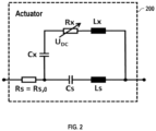
- Fig. 2 shows an equivalent circuit diagram of the actuator 200 according to Fig. 1 , in particular in the region of a resonance point
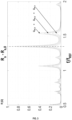
- Fig. 3 shows a diagram for illustrating the mechanical resonances of the actuator 200 according to Fig. 1 .
- the drive device 100 in Fig. 1 comprises a drive unit 110 for applying a drive voltage U DC to the actuator 200 for setting a specific position of the driven actuator 200.
- the drive unit 110 and the actuator 200 are coupled via a first node K1.
- the drive unit 110 is a DC voltage source and the drive voltage U DC is a DC voltage.
- an input resistance R IN is connected between the DC voltage source 110 and the first node K1.
- the actuator 200 can be regarded as a DC-voltage-independent RLC series circuit comprising Rs, Cs and Ls, wherein a further RLC series circuit comprising R x , C x and L x is connected in parallel with the reactive components C S and L S .
- L s and L x shall be lossless, ideal inductances in the simplified actuator equivalent circuit diagram in Fig. 2 .
- the drive device 100 in Fig. 1 furthermore has a source 120 controlled by an excitation signal s(t) and coupled to the first node K1, for feeding a time-dependent AC current signal I(t) into the first node K1 in such a way that a specific AC voltage arises at the actuator 200 as a result of the superposition of the drive voltage U DC and an AC voltage corresponding to a product of the AC current signal I(t) and the impedance Z of the actuator 200.
- the source 120 in Fig. 1 comprises a signal generator 121 controlled by the excitation signal s(t), and a current or voltage source 122 controlled by the output signal AS of the controlled signal generator 121 for outputting the time-dependent AC current signal I(t).
- a coupling capacitance C IN for coupling to the first node K1 is connected between the current or voltage source 122 and the first node K1.
- the drive device 100 in Fig. 1 further has a filter unit 130 connected to the output of the actuator 200 and serving for filtering the output signal A of the actuator 200.
- a determining unit 140 is coupled to the output of the filter unit 130 and is configured to determine an impedance behaviour IV of the actuator 200 depending on the filtered output signal r(t) and to output at its output the excitation signal s(t) for driving the source 120.
- the determining unit 140 is configured to determine the transfer function H (see Fig. 6 ) of a section between the output of the signal generator 121 and the output of the filter unit 130, wherein the section comprises the controlled current or voltage source 122, the coupling capacitance C IN , the first node K1, the actuator 200 and the filter unit 130. Furthermore, the determining unit 140 is configured to determine an inverse I of the determined transfer function H (see Fig. 6 ). In this case, the determining unit 140 is preferably configured to generate the excitation signal s(t) using the calculated inverse I.
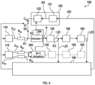
- Fig. 4 shows a schematic block diagram of a second embodiment of a drive device 100 for driving capacitive actuators 200, 205 of an optical system 300.
- the drive device 100 in Fig. 4 is suitable for driving a plurality N of capacitive actuators 200, 205 of the optical system 300, wherein an optical element 310 of the optical system is assigned to each actuator 200, 205 of the plurality N.
- the reference sign 200 denotes the actuator i that is currently to be measured, wherein the reference sign 205 denotes the further (N-1) actuators that are currently not being measured with regard to their impedance behaviour.
- the actuator 200 that is respectively to be measured is selected by means of the switch S.
- a drive unit 110, a filter unit 130, a peak-to-peak detector 150 and an output stage 160 are provided for the actuator 200 to be measured.
- the reference sign 115 denotes a group of drive units for said group 205 of (N-1) actuators.
- the reference sign 135 denotes a group of filter units for said (N-1) actuators
- the reference sign 155 denotes a group of peak-to-peak detectors for said (N-1) actuators 205
- the reference sign 165 denotes a group of output stages for said group of (N-1) actuators.
- the respective actuator 200, 205 is assigned a respective drive unit 110, 115 for applying a drive voltage U DC to the actuator 200, 205 for setting a specific position of the driven actuator 200, 205 and a respective filter unit 130, 135 connected to the output of the actuator 200, 205 and serving for filtering the output signal of the actuator 200, 205.
- the determining unit 140 in Fig. 4 is coupled to the output of the respective filter unit 130, 135.
- the impedance behaviour IV of the actuator i having the reference sign 200 is currently being measured in the case of the switch position of the switch S in Fig. 4 .
- the filter unit 130 is embodied as a high-pass filter for providing a high-pass-filtered output signal r 1 (t).
- a peak-to-peak detector 150 and an output stage 160 connected downstream of the peak-to-peak detector 150 for providing at least one narrowband partial output signal r 2 (t) are connected downstream of the high-pass filter 130.
- the determining unit 140 is configured to carry out a broadband determination of the impedance behaviour IV of the actuator 200 on the basis of the high-pass-filtered output signal r 1 (t) and/or to carry out a narrowband determination of the impedance behaviour IV of the actuator 200 on the basis of the at least one narrowband partial output signal r 2 (t).
- the determining unit 140 samples the outputs of the high-pass filter 130 in order to obtain the signal r 1 (t) and the output of the output stage 160 in order to obtain the signal r 2 (t). Furthermore, the determining unit 140 controls the switches S, wherein the switches S assigned to the N-1 actuators 205 are not depicted in Fig. 4 for illustration reasons, and calculates the respective excitation signal s(t) for the source 120.
- the determining unit 140 is embodied as an SPU (Signal Processing Unit), for example. To summarize, the determining unit 140 controls the switches S and the drive voltages U DC , calculates the excitation signals s(t) for the source 120 and samples the outputs of the high-pass filter 130 and of the output stage 160.
- SPU Signal Processing Unit
- FIG. 5 shows a diagram for illustrating a measurement voltage profile of the filtered output signal r 2 (t) of the actuator 200 according to Fig. 2 .
- Fig. 5 shows a peak value of the measurement voltage profile in the scanning mode: Amplitude measurement value in the settled state for actuator impedances without resonance (variation of the series resistance R s ) in the case of a resonance (variation of the series damping resistance R x ) measured at a chosen measurement frequency.
- a fast broadband image of the actuator resonances can be obtained by means of fast Fourier calculation (FFT; Fast Fourier Transformation) of the output signal r 1 (t).
- the maximum measurement frequency can be of the order of magnitude of MHz, preferably approximately 100 kHz or less.
- the excitation signal s(t) is a sinusoidal signal or preferably an excitation signal calculated by means of inverse Fourier transformation.
- the IFT stimulus is preferably calculated from a predefined excitation frequency profile.
- the sensitivity of the impedance measurement can be particularly increased, for example by way of a frequency response chosen deliberately to be flat in the vicinity of a resonant frequency (cf. Fig. 3 ).
- a flat profile of the output r 2 (t) can be achieved e.g. by the excitation signal s(t) having an inverse excitation frequency profile with respect to the actuator impedance.
- the determining unit 140 in Fig. 4 is able to determine the impedance behaviour IV of the actuator 200 inline and rapidly, in particular in real time. On the basis thereof, it is possible to implement active damping measures against the electromechanical disturbances (see Fig. 3 ) in the actuator resonances that arise as a result of the drive voltage U DC .
- the determining unit 140 is configured in particular to generate the excitation signal s(t) depending on the determined impedance behaviour IV of the actuator 200 in such a way that the AC voltage arising at the actuator 200 has an amplitude that is constant over the frequency.
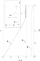
- Fig. 9A shows a diagram for illustrating the theoretical impedance behaviour to be measured of the actuator 200 according to Fig. 4 for a predefined drive voltage U DC .
- the curve 901 shows the impedance of the actuator 200
- the curve 902 shows the real resistance of the actuator
- the curve 903 shows the capacitance (relative to a reference capacitance).
- a broadband excitation signal s(t) for each actuator of interest here for example the actuator 200
- a sufficiently fast digital-to-analogue converter accommodated in the signal generator 121, for example.
- the excitation signal s(t) can then be calculated from the inverse Fourier transformation of the inverse transfer function I and a suitable phase profile ⁇ (f).
- Fig. 7 shows an exemplary embodiment of a suitable phase profile ⁇ (f) for calculating the IFT excitation signal s(t).
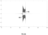
- Fig. 8A shows a diagram for illustrating an exemplary embodiment of a suitable excitation signal s(t) and the AC component I(t)*Z(j ⁇ ) of the resulting response signal r(t).
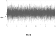
- Fig. 8B illustrates a diagram for illustrating a further exemplary embodiment of a suitable excitation signal s(t).
- Fig. 8B shows a different excitation signal s(t) by comparison with Fig. 8A .
- the excitation signal s(t) in Fig. 8B is based on a different phase function compared with the excitation signal s(t) in Fig. 8A .
- Comparison of Figs. 8A and 8B shows that the energy in Fig. 8B is more distributed over time than in Fig. 8A .
- the excitation signal s(t) in Fig. 8B can also be regarded as a pseudo-noise signal and can also be used permanently during operation of the lithography apparatus.
- phase profile ⁇ (f) can have any desired profile. It is also possible to use different frequency ranges for groups or subgroups of actuators 200, 205, both for excitation and for detection. Frequency-division multiplexing operation can be used for this purpose.
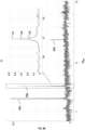
- Fig. 9B and Fig. 9C show diagrams for illustrating the experimentally measured impedance behaviour of the actuator 200 according to Fig. 4 .
- the falling curve 901 represents a theoretical actuator impedance to be measured wherein the fall extends over three orders of magnitude (from 10 k ⁇ down to 10 ⁇ in this exemplary embodiment).
- three very small resonance points of the actuator 200 can be seen for a drive voltage.
- the measured impedance behaviour of the actuator 200 exhibits three resonance points RS1, RS2 and RS3 in Fig. 9B and in Fig. 9C .
- the first resonance point RS1 and the third resonance point RS3 arise for one and the same drive voltage, which can also be referred to as actuator DC voltage and is 75 volts, for example.
- FIG. 9B shows that three different peaks P1 (for a drive voltage of 100 volts), P2 (for a drive voltage of 75 volts) and P3 (for a drive voltage of 50 volts) are able to be differentiated at the resonance point RS2.
- P1 for a drive voltage of 100 volts
- P2 for a drive voltage of 75 volts
- P3 for a drive voltage of 50 volts
- the same is shown by the box showing the enlarged view in Fig. 9C and this emphasizes that at the first resonance point RS1 one peak is caused by a single actuator DC voltage and at the second resonance point RS2 three peaks P1, P2 and P3 are caused by three actuator DC voltages.
- U Stim (t) shall be the excitation signal.
- U DC 0 V
- Fig. 10 shows a schematic block diagram of an embodiment of an optical system 300 comprising a plurality of actuatable optical elements 310.
- the optical system 300 is embodied here as a micromirror array, wherein the optical elements 310 are micromirrors.
- Each micromirror 310 is actuatable by means of an assigned actuator 200.
- a respective micromirror 310 can be tilted about two axes and/or displaced in one, two, or three spatial axes by means of the assigned actuator 200.
- the reference signs only of the topmost row of these elements are depicted, for reasons of clarity.
- the optical system 300 comprises a correction unit 320 configured for generating an input signal E for each of the micromirrors 310.
- the optical system 300 is configured for correcting a wavefront of light in a lithography apparatus 600A, 600B (see Figs. 6A, 6B), wherein the correction unit 320, for example, depending on a measured shape of the wavefront and a target shape of the wavefront, determines a target position of each of the micromirrors 310 and outputs a corresponding input signal E.
- the respective input signal E is fed to a drive device 100 assigned to a respective actuator 200.
- the drive device 100 drives the respective actuator 200 for example with a filtered, amplified modulation signal fPWM.
- the drive device 100 has been described with reference to Figs. 1 to 9 , in particular. A position of the respective micromirror 310 is thus set.
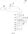
- Fig. 11A shows a schematic view of an EUV lithography apparatus 600A comprising a beam-shaping and illumination system 602 and a projection system 604.
- EUV stands for "extreme ultraviolet” and denotes a wavelength of the working light of between 0.1 nm and 30 nm.
- the beam-shaping and illumination system 602 and the projection system 604 are respectively provided in a vacuum housing (not shown), wherein each vacuum housing is evacuated with the aid of an evacuation device (not shown).
- the vacuum housings are surrounded by a machine room (not shown), in which drive devices for mechanically moving or setting optical elements are provided.
- electrical controllers and the like can also be provided in this machine room.
- the EUV lithography apparatus 600A comprises an EUV light source 606A.
- a plasma source or a synchrotron
- the EUV radiation 608A is focused and the desired operating wavelength is filtered out from the EUV radiation 608A.
- the EUV radiation 608A generated by the EUV light source 606A has a relatively low transmissivity through air, for which reason the beam-guiding spaces in the beam-shaping and illumination system 602 and in the projection system 604 are evacuated.
- the beam-shaping and illumination system 602 illustrated in Fig. 11A has five mirrors 610, 612, 614, 616, 618.
- the EUV radiation 608A is guided onto a photomask (reticle) 620.
- the photomask 620 is likewise embodied as a reflective optical element and can be arranged outside the systems 602, 604.
- the EUV radiation 608A can be directed onto the photomask 620 by means of a mirror 622.
- the photomask 620 has a structure which is imaged onto a wafer 624 or the like in a reduced fashion by means of the projection system 604.
- the projection system 604 (also referred to as a projection lens) has five mirrors M1 to M5 for imaging the photomask 620 onto the wafer 624.
- individual mirrors M1 to M5 of the projection system 604 can be arranged symmetrically in relation to an optical axis 626 of the projection system 604.
- the number of mirrors M1 to M6 of the EUV lithography apparatus 600A is not restricted to the number represented. A greater or lesser number of mirrors M1 to M5 can also be provided.
- the mirrors M1 to M5 are generally curved at their front side for beam shaping.
- the projection system 604 comprises an optical system 300 having a plurality of actuatable optical elements 310, for example the micromirror array described with reference to Fig. 10 .
- the optical system 300 is configured in particular for correcting dynamic imaging aberrations.
- the projection system 604 comprising the optical system 300 can be referred to as an adaptive optical unit.
- a resolution of the lithography apparatus 600A can thereby be increased.
- a correction unit 320 generates an input signal E, which can comprise an individual signal in particular for a respective micromirror 310.
- the input signal E is converted into an amplified, filtered modulation signal fPWM by the drive device 100 for a respective optical element 310, and output to the respective actuator 200 for actuating the optical element 310.
- the respective actuator 200 correspondingly actuates the assigned micromirror 310.
- Fig. 11B shows a schematic view of a DUV lithography apparatus 600B, which comprises a beam-shaping and illumination system 602 and a projection system 604.
- DUV stands for "deep ultraviolet” and denotes a wavelength of the working light of between 30 nm and 250 nm.
- the beam-shaping and illumination system 602 and the projection system 604 can be arranged in a vacuum housing and/or be surrounded by a machine room with corresponding drive devices.
- the DUV lithography apparatus 600B has a DUV light source 606B.
- a DUV light source 606B By way of example, an ArF excimer laser that emits radiation 608B in the DUV range at 193 nm, for example, can be provided as the DUV light source 606B.
- the beam-shaping and illumination system 602 illustrated in Fig. 11B guides the DUV radiation 608B onto a photomask 620.
- the photomask 620 is embodied as a transmissive optical element and can be arranged outside the systems 602, 604.
- the photomask 620 has a structure which is imaged onto a wafer 624 or the like in a reduced fashion by means of the projection system 604.
- the projection system 604 has a plurality of lens elements 628 and/or mirrors 630 for imaging the photomask 620 onto the wafer 624.
- individual lens elements 628 and/or mirrors 630 of the projection system 604 can be arranged symmetrically in relation to an optical axis 626 of the projection system 604.
- the number of lens elements 628 and mirrors 630 of the DUV lithography apparatus 600B is not restricted to the number represented. A greater or lesser number of lens elements 628 and/or mirrors 630 can also be provided.
- the mirrors 630 are generally curved at their front side for beam shaping.
- the projection system 604 comprises an optical system 300 having a plurality of actuatable optical elements 310, for example a microlens element array, which can be constructed in particular according to the micromirror array described with reference to Fig. 10 , wherein microlens elements are used instead of the micromirrors.
- the optical system 300 is configured in particular for correcting dynamic imaging aberrations.
- the projection system 604 comprising the optical system 300 can be referred to as an adaptive optical unit. A resolution of the lithography apparatus 600B can thereby be increased.
- an input signal E is predefined from outside.
- the input signal E comprises, in particular, an individual signal for each of the microlens elements 310 of the optical system 300.
- the drive device 100 converts the signal contained in the input signal E for a respective microlens element 310 into an amplified, filtered modulation signal fPWM and outputs the latter to the respective actuator 200.
- the respective actuator 200 correspondingly actuates the assigned microlens element 310.
- An air gap between the last lens element 628 and the wafer 624 may be replaced by a liquid medium 632 which has a refractive index of > 1.
- the liquid medium 632 may be for example high-purity water. Such a construction is also referred to as immersion lithography and has an increased photolithographic resolution.
- the medium 632 can also be referred to as an immersion liquid.
Landscapes
- Physics & Mathematics (AREA)
- General Physics & Mathematics (AREA)
- Optics & Photonics (AREA)
- Mechanical Light Control Or Optical Switches (AREA)
- Exposure And Positioning Against Photoresist Photosensitive Materials (AREA)
Description
- The present invention relates to a drive device for driving an actuator of an optical system, to an optical system comprising such a drive device, and to a lithography apparatus comprising such an optical system.
- The content of the
priority application DE 10 2020 205 279.4 is being referred to. - Microlithography apparatuses are known which have actuatable optical elements, such as, for example, microlens element arrays or micromirror arrays. Microlithography is used for producing microstructured components, such as, for example, integrated circuits. The microlithography process is performed using a lithography apparatus, which has an illumination system and a projection system. The image of a mask (reticle) illuminated by means of the illumination system is in this case projected by means of the projection system onto a substrate, for example a silicon wafer, which is coated with a light-sensitive layer (photoresist) and arranged in the image plane of the projection system, in order to transfer the mask structure to the light-sensitive coating of the substrate. The imaging of the mask on the substrate can be improved by means of actuatable optical elements. By way of example, wavefront aberrations during exposure, which result in magnified and/or unsharp imagings, can be compensated for.
- Such correction by means of the optical element requires detection of the wavefront and signal processing in order to determine a respective position of an optical element which enables the wavefront to be corrected as desired. In the last step, it is necessary to amplify the drive signal for a respective optical element and to output it to the actuator of the optical element.
- By way of example, a PMN actuator (PMN; lead magnesium niobate) can be used as actuator. A PMN actuator enables distance positioning in the sub-micrometre range or sub-nanometre range. In this case, the actuator, having actuator elements stacked one on top of another, experiences a force that causes a specific linear expansion as a result of a DC voltage being applied. The position set by way of the DC voltage (DC; Direct Current) can be adversely influenced by external electromechanical crosstalk at the fundamentally arising resonance points of the actuator driven by the DC voltage. Owing to this electromechanical crosstalk, precise positioning is no longer able to be set in a stable manner. In this case, the mechanical resonances are all the greater the higher the applied DC voltage. Said resonance points may also change in the long term, for example as a result of temperature drift or as a result of adhesive drift if the mechanical linking of the adhesive material changes, or as a result of hysteresis or ageing. An impedance measurement would be helpful in this context.
- However, conventional impedance measuring devices are often too cost-intensive and furthermore do not have an inline capability, that is to say that they are regularly not able to be used in a lithography apparatus. Furthermore, integrated impedance measuring bridges, which are usually designed for excessively high impedance values, prove not to be suitable for the present application in a lithography apparatus since the impedance value range of interest here encompasses a plurality of orders of magnitude and the range of interest is only a fraction of the total range.
- Document
US 2019/346772 A1 describes an apparatus which comprises a radiation source for generating radiation, a plurality of optical components for guiding the radiation in the apparatus, a number N1 of arrays, where N1≥1, wherein each of the N1 arrays comprises at least one actuator/sensor device which is assigned to one of the optical components, a plurality N2 of local drive units for driving the number N1 of arrays, where N2≥2, and a number N3 of central drive units for driving the N2 local drive units, whereN3A 1. - Document
WO 2009/110787 A1 describes a drive system configured to controllably drive an electric actuator. The drive system comprises a current sensor system configured to sense a current conducted by the electric actuator, the current sensor system comprising at least a first and a second current sensor that have a mutually different sensitivity for the current to be sensed, and a driver configured to electrically drive the electric actuator based on an output signal of the current sensor system, the driver comprising a current sensor controller configured to control an extent to which each of the at least first and second current sensors determines the output signal of the current sensor system. -
Document EP 2 906 994 A1 describes an actuation mechanism to provide movement with at least two degrees of freedom. The mechanism comprises a moving part and a static part, the moving part including a permanent magnet with a magnetic face constrained to move over a working area lying substantially in a first plane perpendicular to a direction of magnetization of the magnet, the static part comprising at least two electromagnets having pole faces lying substantially in a second plane closely parallel to the first plane, the pole faces being symmetrically distributed around a central position in the second plane and extending over substantially the whole area traversed by the face of the moving magnet. - Against this background, it is an object of the present invention to improve the driving of an actuator of an optical system.
- In accordance with a first aspect, a drive device for driving a capacitive actuator of an optical system is proposed. The drive device comprises:
- a drive unit for applying a drive voltage to the actuator for setting a specific position of the driven actuator, wherein the drive unit and the actuator are coupled via a first node,
- a source controlled by an excitation signal and coupled to the first node, for feeding a time-dependent AC current signal into the first node in such a way that a specific AC voltage arises at the actuator as a result of the superposition of the drive voltage and an AC voltage corresponding to a product of the AC current signal and the impedance of the actuator,
- a filter unit connected to the output of the actuator and serving for filtering an output signal of the actuator, and
- a determining unit coupled to an output of the filter unit and configured to determine an impedance behaviour of the actuator depending on the filtered output signal and to output at its output the drive signal for driving the source.
- The actuator is, in particular, a PMN actuator (PMN; lead magnesium niobate) or a PZT actuator (PZT; lead zirconate titanate). The actuator is configured, in particular, to actuate an optical element of the optical system. Examples of such an optical element include lens elements, mirrors and adaptive mirrors.
- The present drive device enables a fast determination, with an inline capability, of the impedance behaviour of the actuator, in particular an impedance measurement of the actuator installed in the lithography apparatus.
- On the basis of the determined impedance behaviour of the actuator, suitable remedies or countermeasures, in particular an active inline calibration or inline damping, can also be implemented by means of the drive signal and a corresponding AC current signal fed in at the first node.
- In accordance with one embodiment, the source comprises a signal generator controlled by the excitation signal, and a current or voltage source controlled by an output signal of the controlled signal generator for outputting the time-dependent AC current signal.
- In accordance with a further embodiment, the determining unit is configured to determine the transfer function of a section between the output of the signal generator and the output of the filter unit, wherein the section comprises the controlled current or voltage source, the first node, the actuator and the filter unit to determine an inverse of the determined transfer function, and to generate the drive signal using the calculated inverse.
- The inverse can also be referred to as an inverse transfer function. As an alternative to the inverse transfer function, it is also possible to use some other transformation of the transfer function which can particularly cause the resonance points of the actuator in order to be able to determine them optimally.
- In accordance with a further embodiment, the transfer function is a frequency-dependent signal transfer function of the drive signal embodied as a time-dependent excitation voltage and of the filtered output signal embodied as a complex excitation response voltage.
- In accordance with a further embodiment, the filter unit is embodied as a high-pass filter for providing a high-pass-filtered output signal.
- Preferably, the determining unit can then determine the impedance behaviour of the actuator depending on the high-pass-filtered output signal.
- In accordance with a further embodiment, a peak-to-peak detector connected downstream of the high-pass filter and an output stage connected downstream of the peak-to-peak detector for providing at least one narrowband partial output signal are provided, wherein the determining unit is configured to carry out a broadband determination of the impedance behaviour of the actuator on the basis of the high-pass-filtered output signal and/or to carry out a narrowband determination of the impedance behaviour of the actuator on the basis of the at least one narrowband partial output signal.
- An inverse Fourier transformation, in particular, is used in the broadband determination of the impedance behaviour of the actuator. For this reason, the broadband determination of the impedance behaviour by the determining unit can also be referred to as an IFT mode (IFT; Inverse Fourier Transformation). Narrow frequency bands can be examined or scanned very accurately in the narrowband determination of the impedance behaviour. For this reason, the narrowband determination of the impedance behaviour by the determining unit can also be referred to as a scanning mode.
- In accordance with a further embodiment, the determining unit is configured to generate the drive signal depending on the determined impedance behaviour of the actuator in such a way that the specific AC voltage arising at the actuator has an amplitude that is constant over the frequency.
- The specific AC voltage having the amplitude that is constant over the frequency has the advantage that very precise positioning of the optical element to be actuated is possible.
- In accordance with a further embodiment, the drive device is configured to control, by open-loop control, the specific AC voltage arising at the actuator to the amplitude that is constant over the frequency using the drive signal.
- In accordance with a further embodiment, the drive device is configured to control, by closed-loop control, the specific AC voltage arising at the actuator to the amplitude that is constant over the frequency using the drive signal.
- Depending on the application, the specific AC voltage can be controlled to the amplitude that is constant over the frequency by open-loop or closed-loop control. Suitable active inline damping measures are made possible as a result.
- In accordance with a further embodiment, the drive unit comprises a DC voltage source. Furthermore, an input resistance is coupled between the DC voltage source and the first node.
- In accordance with a further embodiment, the source comprises a controllable voltage or current source. Moreover, a coupling capacitance is connected between the voltage or current source and the first node.
- In accordance with a further embodiment, the drive device is configured to drive a plurality N of capacitive actuators of the optical system. In this case, an optical element of the optical system is assigned to each actuator. By way of example, N = 100.
- In accordance with a further embodiment, the respective actuator is assigned a respective drive unit for applying a drive voltage to the actuator for setting a specific position of the driven actuator and a respective filter unit connected to the output of the actuator and serving for filtering an output signal of the actuator. In this case, the determining unit is coupled to the output of the respective filter unit and is configured to determine the impedance behaviour of the respective actuator depending on the respective filtered output signal and to output at its output the drive signal for the respective actuator.
- The determining unit can in particular select the actuator to be measured, for example by way of a number of switches that can be driven by the determining unit. In particular, the determining unit is configured to drive said switches, to drive the drive units, to calculate the excitation signals and to sample the outputs of the filter units. The determining unit is embodied as an SPU (Signal Processing Unit), for example.
- In this case, the excitation signal is preferably an excitation signal calculated by means of the inverse Fourier transformation (IFT stimulus). In this case, the IFT stimulus is preferably calculated from a predefined excitation frequency profile, wherein a suitably chosen excitation profile can particularly increase the sensitivity of the impedance measurement, for example by way of a frequency response chosen deliberately to be flat in the vicinity of a resonant frequency.
- In accordance with a further embodiment, the respective first node is connectable to the source by means of a respective controllable switch. In this case, the determining unit is configured, for the purpose of determining the impedance behaviour of a specific actuator of the plurality of actuators, to drive the drive unit assigned to the specific actuator and the switch assigned to the specific actuator.
- The respective unit, for example the determining unit, can be implemented in terms of hardware technology and/or else in terms of software technology or as a combination of the two. In the case of an implementation in terms of hardware technology, the respective unit can be embodied as a device or as part of a device, for example as a computer or as a microprocessor. In the case of an implementation in terms of software technology, the respective unit or a part of the unit can be embodied as a computer program product, as a function, as a routine, as an independent process, as part of a program code and/or as an executable object.
- In accordance with a second aspect, an optical system comprising a number of actuatable optical elements is proposed. Each of the actuatable optical elements of the number is assigned an actuator and each actuator is assigned a drive device for driving the actuator in accordance with the first aspect or one of the embodiments of the first aspect.
- The optical system comprises, in particular, a micromirror array and/or a microlens element array having a multiplicity of optical elements that are actuatable independently of one another.
- In embodiments, groups of actuators can be defined, wherein all actuators of a group are assigned the same drive device.
- In accordance with a third aspect, a lithography apparatus comprising an optical system in accordance with the second aspect is proposed.
- A lithography apparatus comprises an illumination system and an imaging system, for example. The illumination system comprises, in particular, a light source and a beam-shaping optical unit. The imaging system comprises, in particular, an imaging optical unit for imaging the mask onto the substrate.
- The optical system can be used in the illumination system, in the beam-shaping optical unit, and also in the imaging system. In preferred embodiments, the optical system is embodied as a microlens element array or a micromirror array and serves for example for wavefront correction in the imaging system.
- The lithography apparatus is for example an EUV lithography apparatus, the working light of which is in a wavelength range of 0.1 nm to 30 nm, or a DUV lithography apparatus, the working light of which is in a wavelength range of 30 nm to 250 nm.
- Preferably, the lithography apparatus additionally comprises a measuring system configured for detecting a wavefront and configured for outputting a correction signal for correcting the wavefront by means of the optical system. The correction signal can serve in particular as the input signal for the drive device.
- "A(n); one" in the present case should not necessarily be understood as restrictive to exactly one element. Rather, a plurality of elements, such as, for example, two, three or more, can also be provided. Any other numeral used here, too, should not be understood to the effect that there is a restriction to exactly the stated number of elements. Rather, numerical deviations upwards and downwards are possible, unless indicated to the contrary.
- Further possible implementations of the invention also comprise not explicitly mentioned combinations of features or embodiments that are described above or below with respect to the exemplary embodiments. In this case, a person skilled in the art will also add individual aspects as improvements or supplementations to the respective basic form of the invention.
- Further advantageous configurations and aspects of the invention are the subject matter of the dependent claims and also of the exemplary embodiments of the invention described below. In the text that follows, the invention is explained in more detail on the basis of preferred embodiments with reference to the accompanying figures.
-
Fig. 1 shows a schematic block diagram of a first embodiment of a drive device for driving a capacitive actuator of an optical system; -
Fig. 2 shows an equivalent circuit diagram to a first approximation of an actuator according toFig. 1 ; -
Fig. 3 shows a diagram for illustrating the control-voltage-dependent, electromechanical resonances of an actuator according toFig. 1 ; -
Fig. 4 shows a schematic block diagram of a second embodiment of a drive device for driving capacitive actuators of an optical system; -
Fig. 5 shows a diagram for illustrating a measurement voltage profile of the filtered output signal of an actuator according toFig. 4 ; -
Fig. 6 shows a diagram for illustrating a determined transfer function and the inverse thereof for generating the excitation signal according toFig. 4 ; -
Fig. 7 shows a diagram for illustrating an exemplary embodiment of a suitable phase profile for generating the excitation signal according toFig. 4 ; -
Fig. 8A shows a diagram for illustrating an exemplary embodiment of a suitable excitation signal and the AC component of the resulting response signal; -
Fig. 8B shows a diagram for illustrating a further exemplary embodiment of a suitable excitation signal; -
Fig. 9A shows a diagram for illustrating the theoretical impedance behaviour to be measured of an actuator according toFig. 4 for a predefined drive voltage; -
Fig. 9B shows a first diagram for illustrating an experimentally measured impedance behaviour of an actuator according toFig. 4 for predefined drive voltages; -
Fig. 9C shows a second diagram for illustrating the experimentally measured impedance behaviour of the actuator according toFig. 4 for predefined drive voltages; -
Fig. 10 shows a schematic block diagram of an embodiment of an optical system; -
Fig. 11A shows a schematic view of an embodiment of an EUV lithography apparatus and -
Fig. 11B shows a schematic view of an embodiment of a DUV lithography apparatus. - Identical elements or elements having an identical function have been provided with the same reference signs in the figures, unless indicated to the contrary. It should also be noted that the illustrations in the figures are not necessarily true to scale.
-
Fig. 1 shows a schematic block diagram of a first embodiment of adrive device 100 for driving acapacitive actuator 200 of anoptical system 300. Examples of anoptical system 300 are shown inFigs. 10 ,11A and11B . - The
actuator 200 can be, for example, a PMN actuator (PMN; lead magnesium niobate) or a PZT actuator (PZT; lead zirconate titanate). Theactuator 200 is suitable for actuating anoptical element 310, such as, for example, a lens element, a mirror or an adaptive mirror. - The first embodiment of the
drive device 100 in accordance withFig. 1 is also explained below with reference toFigs. 2 and3 and the further figures. In this case,Fig. 2 shows an equivalent circuit diagram of theactuator 200 according toFig. 1 , in particular in the region of a resonance point, andFig. 3 shows a diagram for illustrating the mechanical resonances of theactuator 200 according toFig. 1 . - The
drive device 100 inFig. 1 comprises adrive unit 110 for applying a drive voltage UDC to theactuator 200 for setting a specific position of the drivenactuator 200. Thedrive unit 110 and theactuator 200 are coupled via a first node K1. - In the example in
Fig. 1 , thedrive unit 110 is a DC voltage source and the drive voltage UDC is a DC voltage. In this case, an input resistance RIN is connected between theDC voltage source 110 and the first node K1. - In accordance with the equivalent circuit diagram in
Fig. 2 , theactuator 200 can be regarded as a DC-voltage-independent RLC series circuit comprising Rs, Cs and Ls, wherein a further RLC series circuit comprising Rx, Cx and Lx is connected in parallel with the reactive components CS and LS. In accordance with the equivalent circuit diagram inFig. 2 , Ls and Lx shall be lossless, ideal inductances in the simplified actuator equivalent circuit diagram inFig. 2 . - The text hereinafter demonstrates that the dynamic range of the impedance measurement and the measurement speed can be particularly increased by means of the measurement architecture in
Fig. 1 (and inFig. 4 ) and a correspondingly chosen excitation signal s(t) (seeFig. 8A , for example). - The influence of the drive voltage UDC on the resonance points (see
Fig. 3 ) will firstly be considered in a decoupled way, proceeding from the impedance behaviour IV to be measured (seeFig. 9 ) of theactuator 200. As a result of introducing the purely resistive influence - to be considered firstly in a virtual fashion - of the series resistance Rs in accordance withFig. 2 and the associated resonance manifestation, by means of the likewise virtual voltage-dependent series damping resistance Rx it is possible to design the measurement architecture in accordance withFig. 1 , which can be used to carry out suitable impedance measurements of theactuator 200, for example in accordance withFig. 9 . - The
drive device 100 inFig. 1 furthermore has asource 120 controlled by an excitation signal s(t) and coupled to the first node K1, for feeding a time-dependent AC current signal I(t) into the first node K1 in such a way that a specific AC voltage arises at theactuator 200 as a result of the superposition of the drive voltage UDC and an AC voltage corresponding to a product of the AC current signal I(t) and the impedance Z of theactuator 200. - The
source 120 inFig. 1 comprises asignal generator 121 controlled by the excitation signal s(t), and a current orvoltage source 122 controlled by the output signal AS of the controlledsignal generator 121 for outputting the time-dependent AC current signal I(t). A coupling capacitance CIN for coupling to the first node K1 is connected between the current orvoltage source 122 and the first node K1. - The
drive device 100 inFig. 1 further has afilter unit 130 connected to the output of theactuator 200 and serving for filtering the output signal A of theactuator 200. - A determining
unit 140 is coupled to the output of thefilter unit 130 and is configured to determine an impedance behaviour IV of theactuator 200 depending on the filtered output signal r(t) and to output at its output the excitation signal s(t) for driving thesource 120. - In particular, the determining
unit 140 is configured to determine the transfer function H (seeFig. 6 ) of a section between the output of thesignal generator 121 and the output of thefilter unit 130, wherein the section comprises the controlled current orvoltage source 122, the coupling capacitance CIN, the first node K1, theactuator 200 and thefilter unit 130. Furthermore, the determiningunit 140 is configured to determine an inverse I of the determined transfer function H (seeFig. 6 ). In this case, the determiningunit 140 is preferably configured to generate the excitation signal s(t) using the calculated inverse I. -
Fig. 4 shows a schematic block diagram of a second embodiment of adrive device 100 for drivingcapacitive actuators optical system 300. - The
drive device 100 inFig. 4 is suitable for driving a plurality N ofcapacitive actuators optical system 300, wherein anoptical element 310 of the optical system is assigned to each actuator 200, 205 of the plurality N. - In
Fig. 4 , thereference sign 200 denotes the actuator i that is currently to be measured, wherein thereference sign 205 denotes the further (N-1) actuators that are currently not being measured with regard to their impedance behaviour. Theactuator 200 that is respectively to be measured is selected by means of the switch S. Adrive unit 110, afilter unit 130, a peak-to-peak detector 150 and anoutput stage 160 are provided for theactuator 200 to be measured. - Analogously to the
reference sign 205 denoting the group of (N-1) actuators, thereference sign 115 denotes a group of drive units for saidgroup 205 of (N-1) actuators. Correspondingly, thereference sign 135 denotes a group of filter units for said (N-1) actuators, thereference sign 155 denotes a group of peak-to-peak detectors for said (N-1)actuators 205, and thereference sign 165 denotes a group of output stages for said group of (N-1) actuators. - Therefore, the
respective actuator respective drive unit actuator actuator respective filter unit actuator actuator - The determining
unit 140 inFig. 4 is coupled to the output of therespective filter unit - As already explained above, the impedance behaviour IV of the actuator i having the
reference sign 200 is currently being measured in the case of the switch position of the switch S inFig. 4 . - In the example in
Fig. 4 , thefilter unit 130 is embodied as a high-pass filter for providing a high-pass-filtered output signal r1(t). A peak-to-peak detector 150 and anoutput stage 160 connected downstream of the peak-to-peak detector 150 for providing at least one narrowband partial output signal r2(t) are connected downstream of the high-pass filter 130. In this case, the determiningunit 140 is configured to carry out a broadband determination of the impedance behaviour IV of theactuator 200 on the basis of the high-pass-filtered output signal r1(t) and/or to carry out a narrowband determination of the impedance behaviour IV of theactuator 200 on the basis of the at least one narrowband partial output signal r2(t). In this case, the determiningunit 140 samples the outputs of the high-pass filter 130 in order to obtain the signal r1(t) and the output of theoutput stage 160 in order to obtain the signal r2(t). Furthermore, the determiningunit 140 controls the switches S, wherein the switches S assigned to the N-1actuators 205 are not depicted inFig. 4 for illustration reasons, and calculates the respective excitation signal s(t) for thesource 120. - The determining
unit 140 is embodied as an SPU (Signal Processing Unit), for example. To summarize, the determiningunit 140 controls the switches S and the drive voltages UDC, calculates the excitation signals s(t) for thesource 120 and samples the outputs of the high-pass filter 130 and of theoutput stage 160. - Overall, in the case of the
drive device 100 inFig. 4 for fast inline measurement of the impedance behaviour IV of theindividual actuator - 1. Dedicated inline impedance measurement with applied DC+AC voltage comprising drive voltage UDC and the AC voltage I(t) * Z. Application measurement frequencies of the order of magnitude of Hz to 100 kHz are covered here.
- 2. A broadband, low-noise controllable current or
voltage source 122 is used as part of thesource 120. - 3. The measurement signal (amplitude response and phase response) of the current or voltage profile arising at the actuator impedance is coupled out at the
outputs - 4. The measurement of the voltage dropped across the
actuator 200 can be carried out either in a narrowband fashion by way of the signal r2(t) (also referred to as scanning mode, e.g. by means of the sinusoidal excitation signal) or else in a broadband fashion by means of the signal r1(t) (also referred to as IFT mode, e.g. by means of inverse Fourier transformation). - Referring to the equivalent circuit diagram in
Fig. 2 , the decoupling of the impedance alteration of the purely resistive influence - to be considered firstly in a virtual fashion - of the series resistance Rs (= RS,0 in the zero voltage state) and the associated resonance manifestation is achieved by means of the likewise virtual control-voltage-dependent series damping resistance Rx in that theactuator 200, as already explained above, is regarded as a DC-voltage-independent RLC series circuit (Rs, Cs and Ls) (cf.Fig. 2 ) and the further RLC series circuit comprising Rx, Cx and Lx is connected in parallel with the reactive components Cs and Ls. - Variation of Rx thus simulates the DC voltage influence to a first approximation; if the resistance Rx decreases (with higher UDC), the resonance is amplified; by contrast, if the resistance Rx increases (with lower UDC), a lower manifestation of the resonance results. In this respect,
Fig. 5 shows a diagram for illustrating a measurement voltage profile of the filtered output signal r2(t) of theactuator 200 according toFig. 2 . - The following can equivalently be formulated: An increase in the drive voltage UDC of the
actuator 200 which results in a slight variation of the real Rs accordingly causes a slight decrease in Rx which in turn results in a strong manifestation of the resonances in theactuator 200. In this respect,Fig. 5 shows a peak value of the measurement voltage profile in the scanning mode: Amplitude measurement value in the settled state for actuator impedances without resonance (variation of the series resistance Rs) in the case of a resonance (variation of the series damping resistance Rx) measured at a chosen measurement frequency. - For a suitable design of the coupling capacitance CIN and of the input resistances RIN, the following may hold true:

- One example in this respect: CIN >_ 10 * Cs and RIN ≥ N * Rs for a number of N actuators, as shown in
Fig. 4 , in order to ensure a sufficient coupling of the excitation signal (sinusoidal or calculated by IFT). - A fast broadband image of the actuator resonances can be obtained by means of fast Fourier calculation (FFT; Fast Fourier Transformation) of the output signal r1(t). The maximum measurement frequency can be of the order of magnitude of MHz, preferably approximately 100 kHz or less. In this case, the excitation signal s(t) is a sinusoidal signal or preferably an excitation signal calculated by means of inverse Fourier transformation. The IFT stimulus is preferably calculated from a predefined excitation frequency profile. In this case, by means of a suitably chosen profile, the sensitivity of the impedance measurement can be particularly increased, for example by way of a frequency response chosen deliberately to be flat in the vicinity of a resonant frequency (cf.
Fig. 3 ). A flat profile of the output r2(t) can be achieved e.g. by the excitation signal s(t) having an inverse excitation frequency profile with respect to the actuator impedance. - As explained above, the determining
unit 140 inFig. 4 is able to determine the impedance behaviour IV of theactuator 200 inline and rapidly, in particular in real time. On the basis thereof, it is possible to implement active damping measures against the electromechanical disturbances (seeFig. 3 ) in the actuator resonances that arise as a result of the drive voltage UDC. - In this case, the determining
unit 140 is configured in particular to generate the excitation signal s(t) depending on the determined impedance behaviour IV of theactuator 200 in such a way that the AC voltage arising at theactuator 200 has an amplitude that is constant over the frequency. In this respect,Fig. 9A shows a diagram for illustrating the theoretical impedance behaviour to be measured of theactuator 200 according toFig. 4 for a predefined drive voltage UDC. In detail, inFig. 9A , thecurve 901 shows the impedance of theactuator 200, thecurve 902 shows the real resistance of the actuator and thecurve 903 shows the capacitance (relative to a reference capacitance). - Thus, in order to carry out a faster measurement of all actuator resonances in the frequency range of interest, the impedance measurement architecture in accordance with
Fig. 4 can be used. In this case, in particular, a broadband excitation signal s(t) for each actuator of interest, here for example theactuator 200, is calculated by means of inverse Fourier transformation proceeding from an excitation frequency profile and is transferred to a sufficiently fast digital-to-analogue converter, accommodated in thesignal generator 121, for example. - By means of a fast Fourier transformation of the output signal r1(t), for each actuator with an applied drive voltage UDC in the frequency range of interest all resonance points are determined in real time:
An initial transfer function H of the section between the output of thesignal generator 121 and the output of the high-pass filter 130 is determined, in particular with a drive voltage UDC of 0 V or for Rs = Rs,0. - The inverse transfer function or inverse I (see
Fig. 6 ) of the initial transfer function H is then calculated. - The excitation signal s(t) can then be calculated from the inverse Fourier transformation of the inverse transfer function I and a suitable phase profile Φ(f). In this respect,
Fig. 7 shows an exemplary embodiment of a suitable phase profile Φ(f) for calculating the IFT excitation signal s(t). - In this respect,
Fig. 8A shows a diagram for illustrating an exemplary embodiment of a suitable excitation signal s(t) and the AC component I(t)*Z(jΩ) of the resulting response signal r(t). - Moreover,
Fig. 8B illustrates a diagram for illustrating a further exemplary embodiment of a suitable excitation signal s(t).Fig. 8B shows a different excitation signal s(t) by comparison withFig. 8A . The excitation signal s(t) inFig. 8B is based on a different phase function compared with the excitation signal s(t) inFig. 8A . Comparison ofFigs. 8A and8B shows that the energy inFig. 8B is more distributed over time than inFig. 8A . The excitation signal s(t) inFig. 8B can also be regarded as a pseudo-noise signal and can also be used permanently during operation of the lithography apparatus. - Alternatively, it is also possible to use, instead of the inverse transfer function I with respect to the transfer function H, some other transformation of H that can particularly cause the resonance points of the
actuator 200. In this case, the phase profile Φ(f) can have any desired profile. It is also possible to use different frequency ranges for groups or subgroups ofactuators - In this respect,
Fig. 9B andFig. 9C show diagrams for illustrating the experimentally measured impedance behaviour of theactuator 200 according toFig. 4 . As shown inFig. 9A , the fallingcurve 901 represents a theoretical actuator impedance to be measured wherein the fall extends over three orders of magnitude (from 10 kΩ down to 10 Ω in this exemplary embodiment). As can be gathered from the box showing an enlarged view inFig. 9A , three very small resonance points of theactuator 200 can be seen for a drive voltage. - In this context, the impedance behaviour of an
actuator 200 according toFig. 4 was measured in an experiment for predefined drive voltages. - The measured impedance behaviour of the actuator 200 exhibits three resonance points RS1, RS2 and RS3 in
Fig. 9B and inFig. 9C . The first resonance point RS1 and the third resonance point RS3 arise for one and the same drive voltage, which can also be referred to as actuator DC voltage and is 75 volts, for example. The second resonance point RS2 at f/fREF = 3.1 arises for three different drive voltages or actuator DC voltages of, for example, 50 volts, 75 volts and 100 volts. The box showing an enlarged view inFig. 9B shows that three different peaks P1 (for a drive voltage of 100 volts), P2 (for a drive voltage of 75 volts) and P3 (for a drive voltage of 50 volts) are able to be differentiated at the resonance point RS2. The same is shown by the box showing the enlarged view inFig. 9C and this emphasizes that at the first resonance point RS1 one peak is caused by a single actuator DC voltage and at the second resonance point RS2 three peaks P1, P2 and P3 are caused by three actuator DC voltages. - Overall, the experiment in accordance with
Fig. 9B and in accordance withFig. 9C shows how the impedance measurement values for an IFT excitation with a length of just under 50 milliseconds, for example, can be correctly mapped. - An example of a computation algorithm for the excitation signal s(t) is presented below:
- UStim (t) := s(t) shall be the output voltage of the high-pass filter 130 - also the input voltage for the
source 120; - Uout (jω) shall be the complex excitation response voltage at the output of the high-
pass filter 130; - Ho (jω) shall be the frequency-dependent signal transfer function of UStim(jω) with respect to the output signal of the high-
pass filter 130; - ZAct shall be the actuator impedance;
- Zo shall be a fixed, selected reference resistance (e.g. 10Ω or 50Ω);
- α shall be a constant transfer factor and
- UStim,o shall be a voltage amplitude set by the
SPU 140. - s(t) := UStim(t) shall be the excitation signal. The following equations hold true in this exemplary embodiment:


- This results in an, as shown in
Fig. 9A , almost flat profile of the frequency response apart from the resonance points of theactuator 200 that are to be particularly emphasized. -
Fig. 10 shows a schematic block diagram of an embodiment of anoptical system 300 comprising a plurality of actuatableoptical elements 310. Theoptical system 300 is embodied here as a micromirror array, wherein theoptical elements 310 are micromirrors. Eachmicromirror 310 is actuatable by means of an assignedactuator 200. By way of example, arespective micromirror 310 can be tilted about two axes and/or displaced in one, two, or three spatial axes by means of the assignedactuator 200. The reference signs only of the topmost row of these elements are depicted, for reasons of clarity. - The
optical system 300 comprises acorrection unit 320 configured for generating an input signal E for each of themicromirrors 310. By way of example, theoptical system 300 is configured for correcting a wavefront of light in alithography apparatus correction unit 320, for example, depending on a measured shape of the wavefront and a target shape of the wavefront, determines a target position of each of themicromirrors 310 and outputs a corresponding input signal E. - The respective input signal E is fed to a
drive device 100 assigned to arespective actuator 200. Thedrive device 100 drives therespective actuator 200 for example with a filtered, amplified modulation signal fPWM. Thedrive device 100 has been described with reference toFigs. 1 to 9 , in particular. A position of therespective micromirror 310 is thus set. -
Fig. 11A shows a schematic view of anEUV lithography apparatus 600A comprising a beam-shaping andillumination system 602 and aprojection system 604. In this case, EUV stands for "extreme ultraviolet" and denotes a wavelength of the working light of between 0.1 nm and 30 nm. The beam-shaping andillumination system 602 and theprojection system 604 are respectively provided in a vacuum housing (not shown), wherein each vacuum housing is evacuated with the aid of an evacuation device (not shown). The vacuum housings are surrounded by a machine room (not shown), in which drive devices for mechanically moving or setting optical elements are provided. Moreover, electrical controllers and the like can also be provided in this machine room. - The
EUV lithography apparatus 600A comprises an EUVlight source 606A. A plasma source (or a synchrotron), which emitsradiation 608A in the EUV range (extreme ultraviolet range), that is to say for example in the wavelength range of 5 nm to 20 nm, can for example be provided as the EUVlight source 606A. In the beam-shaping andillumination system 602, theEUV radiation 608A is focused and the desired operating wavelength is filtered out from theEUV radiation 608A. TheEUV radiation 608A generated by the EUVlight source 606A has a relatively low transmissivity through air, for which reason the beam-guiding spaces in the beam-shaping andillumination system 602 and in theprojection system 604 are evacuated. - The beam-shaping and
illumination system 602 illustrated inFig. 11A has fivemirrors illumination system 602, theEUV radiation 608A is guided onto a photomask (reticle) 620. Thephotomask 620 is likewise embodied as a reflective optical element and can be arranged outside thesystems EUV radiation 608A can be directed onto thephotomask 620 by means of amirror 622. Thephotomask 620 has a structure which is imaged onto awafer 624 or the like in a reduced fashion by means of theprojection system 604. - The projection system 604 (also referred to as a projection lens) has five mirrors M1 to M5 for imaging the
photomask 620 onto thewafer 624. In this case, individual mirrors M1 to M5 of theprojection system 604 can be arranged symmetrically in relation to anoptical axis 626 of theprojection system 604. It should be noted that the number of mirrors M1 to M6 of theEUV lithography apparatus 600A is not restricted to the number represented. A greater or lesser number of mirrors M1 to M5 can also be provided. Furthermore, the mirrors M1 to M5 are generally curved at their front side for beam shaping. - Furthermore, the
projection system 604 comprises anoptical system 300 having a plurality of actuatableoptical elements 310, for example the micromirror array described with reference toFig. 10 . Theoptical system 300 is configured in particular for correcting dynamic imaging aberrations. Theprojection system 604 comprising theoptical system 300 can be referred to as an adaptive optical unit. A resolution of thelithography apparatus 600A can thereby be increased. By way of example, depending on measured values of the wavefront of the projection light, acorrection unit 320 generates an input signal E, which can comprise an individual signal in particular for arespective micromirror 310. The input signal E is converted into an amplified, filtered modulation signal fPWM by thedrive device 100 for a respectiveoptical element 310, and output to therespective actuator 200 for actuating theoptical element 310. Therespective actuator 200 correspondingly actuates the assignedmicromirror 310. -
Fig. 11B shows a schematic view of aDUV lithography apparatus 600B, which comprises a beam-shaping andillumination system 602 and aprojection system 604. In this case, DUV stands for "deep ultraviolet" and denotes a wavelength of the working light of between 30 nm and 250 nm. As has already been described with reference toFig. 11A , the beam-shaping andillumination system 602 and theprojection system 604 can be arranged in a vacuum housing and/or be surrounded by a machine room with corresponding drive devices. - The
DUV lithography apparatus 600B has a DUVlight source 606B. By way of example, an ArF excimer laser that emitsradiation 608B in the DUV range at 193 nm, for example, can be provided as the DUVlight source 606B. - The beam-shaping and
illumination system 602 illustrated inFig. 11B guides theDUV radiation 608B onto aphotomask 620. Thephotomask 620 is embodied as a transmissive optical element and can be arranged outside thesystems photomask 620 has a structure which is imaged onto awafer 624 or the like in a reduced fashion by means of theprojection system 604. - The
projection system 604 has a plurality oflens elements 628 and/or mirrors 630 for imaging thephotomask 620 onto thewafer 624. In this case,individual lens elements 628 and/or mirrors 630 of theprojection system 604 can be arranged symmetrically in relation to anoptical axis 626 of theprojection system 604. It should be noted that the number oflens elements 628 and mirrors 630 of theDUV lithography apparatus 600B is not restricted to the number represented. A greater or lesser number oflens elements 628 and/or mirrors 630 can also be provided. Furthermore, themirrors 630 are generally curved at their front side for beam shaping. - Furthermore, the
projection system 604 comprises anoptical system 300 having a plurality of actuatableoptical elements 310, for example a microlens element array, which can be constructed in particular according to the micromirror array described with reference toFig. 10 , wherein microlens elements are used instead of the micromirrors. Theoptical system 300 is configured in particular for correcting dynamic imaging aberrations. Theprojection system 604 comprising theoptical system 300 can be referred to as an adaptive optical unit. A resolution of thelithography apparatus 600B can thereby be increased. In order to improve the imaging performance, in the present case an input signal E is predefined from outside. The input signal E comprises, in particular, an individual signal for each of themicrolens elements 310 of theoptical system 300. Thedrive device 100 converts the signal contained in the input signal E for arespective microlens element 310 into an amplified, filtered modulation signal fPWM and outputs the latter to therespective actuator 200. Therespective actuator 200 correspondingly actuates the assignedmicrolens element 310. - An air gap between the
last lens element 628 and thewafer 624 may be replaced by aliquid medium 632 which has a refractive index of > 1. Theliquid medium 632 may be for example high-purity water. Such a construction is also referred to as immersion lithography and has an increased photolithographic resolution. The medium 632 can also be referred to as an immersion liquid. - Although the present invention has been described on the basis of exemplary embodiments, it is modifiable in diverse ways.
-
- 100
- Drive device
- 110
- Drive unit
- 115
- Group of drive units
- 120
- Source
- 121
- Signal generator
- 122
- Controlled current or voltage source
- 130
- Filter unit
- 135
- Group of filter units
- 140
- Determining unit
- 150
- Peak-to-peak detector
- 155
- Group of peak-to-peak detectors
- 160
- Output stage
- 165
- Group of output stages
- 200
- Actuator
- 205
- Group of N-1 actuators
- 300
- Optical system
- 310
- Optical element
- 320
- Correction unit
- 600A
- EUV lithography apparatus
- 600B
- DUV lithography apparatus
- 602
- Beam-shaping and illumination system
- 604
- Projection system
- 606A
- EUV light source
- 606B
- DUV light source
- 608A
- EUV radiation
- 608B
- DUV radiation
- 610
- Mirror
- 612
- Mirror
- 614
- Mirror
- 616
- Mirror
- 618
- Mirror
- 620
- Photomask
- 622
- Mirror
- 624
- Wafer
- 626
- Optical axis
- 628
- Lens element
- 630
- Mirror
- 632
- Medium
- 901
- Curve
- 902
- Curve
- 903
- Curve
- A
- Output signal
- aPWM
- Amplified signal
- AS
- Output signal of the controlled signal generator
- CIN
- Coupling capacitance
- Cs
- Capacitance
- Cx
- Capacitance
- E
- Input signal
- f
- Frequency
- fPWM
- Filtered signal
- fREF
- Reference frequency
- H
- Transfer function
- I
- Inverse of the transfer function
- I(t)
- AC current signal
- IV
- Impedance behaviour
- K1
- First node
- K2
- Second node
- K3
- Third node
- Ls
- Inductance
- Lx
- Inductance
- M1
- Mirror
- M2
- Mirror
- M3
- Mirror
- M4
- Mirror
- M5
- Mirror
- P1
- Peak
- P2
- Peak
- P3
- Peak
- r(t)
- Filtered output signal
- r1(t)
- High-pass-filtered output signal
- r2(t)
- Narrowband output signal
- RIN
- Input resistance
- Rs
- Resistance
- Rs,0
- Resistance in the zero voltage state
- RS1
- Resonance point
- RS2
- Resonance point
- RS3
- Resonance point
- Rx
- Resistance
- S
- Switch
- s(t)
- Drive signal
- UDC
- Drive voltage
- UDC,1
- Drive voltage
- UDC,2
- Drive voltage
- UDC,3
- Drive voltage
- Z
- Impedance of the actuator
Claims (15)
- Drive device (100) for driving a capacitive actuator (200) for actuating an optical element (310) of an optical system (300), comprisinga drive unit (110) for applying a drive voltage (UDC) to the actuator (200) for setting a specific position of the driven actuator (200), wherein the drive unit (110) and the actuator (200) are coupled via a first node (K1),
characterized bya source (120) being configured to be controlled by an excitation signal (s(t)) and coupled to the first node (K1), for feeding a time-dependent AC current signal (I(t)) into the first node (K1) in such a way that a specific AC voltage arises at the actuator (200) as a result of the superposition of the drive voltage (UDC) and an AC voltage corresponding to a product of the AC current signal (I(t)) and the impedance (Z) of the actuator (200),a filter unit (130) connected to the output of the actuator (200) and being configured to serve for filtering an output signal (A) of the actuator (200), anda determining unit (140) coupled to an output of the filter unit (130) and configured to determine an impedance behaviour (IV) of the actuator (200) depending on the filtered output signal (r(t)) and to output at its output the excitation signal (s(t)) for driving the source (120). - Drive device according to Claim 1,
wherein the source (120) comprises a signal generator (121) being configured to be controlled by the excitation signal (s(t)), and a current or voltage source (122) being configured to be controlled by an output signal (AS) of the controlled signal generator (121) for outputting the time-dependent AC current signal (I(t)). - Drive device according to Claim 2,
wherein the determining unit (140) is configuredto determine the transfer function (H) of a section between the output of the signal generator (121) and the output of the filter unit (130), wherein the section comprises the controlled current or voltage source (122), the first node (K1), the actuator (200) and the filter unit (130),to determine an inverse (I) of the determined transfer function (H), andto generate the excitation signal (s(t)) using the calculated inverse (I). - Drive device according to Claim 3,
wherein the transfer function (H) is a frequency-dependent signal transfer function of the excitation signal (s(t)) embodied as a time-dependent excitation voltage and of the filtered output signal (r(t)) embodied as a complex excitation response voltage. - Drive device according to any of Claims 1 to 4,
wherein the filter unit (130) is configured to be a high-pass filter for providing a high-pass-filtered output signal (r1(t)). - Drive device according to Claim 5,wherein a peak-to-peak detector (150) connected downstream of the high-pass filter (130) and an output stage (160) connected downstream of the peak-to-peak detector (150) for providing at least one narrowband partial output signal (r2(t)) are provided,wherein the determining unit (140) is configured to carry out a broadband determination of the impedance behaviour (IV) of the actuator (200) on the basis of the high-pass-filtered output signal (r1(t)) and/or to carry out a narrowband determination of the impedance behaviour (IV) of the actuator (200) on the basis of the at least one narrowband partial output signal (r2(t)).
- Drive device according to any of Claims 1 to 6,
wherein the determining unit (140) is configured to generate the excitation signal (s(t)) depending on the determined impedance behaviour (IV) of the actuator (200) in such a way that the specific AC voltage arising at the actuator (200) has an amplitude that is constant over the frequency. - Drive device according to Claim 7,
wherein the drive device (100) is configured to control, by open-loop or closed-loop control, the specific AC voltage arising at the actuator (200) to the amplitude that is constant over the frequency using the excitation signal (s(t)). - Drive device according to any of Claims 1 to 8,
wherein the drive unit (110) comprises a DC voltage source and an input resistance (Rin) is connected between the DC voltage source (110) and the first node (K1). - Drive device according to any of Claims 1 to 9,
wherein the source (120) comprises a controllable voltage or current source (122) and a coupling capacitance (CIN) is connected between the voltage or current source (122) and the first node (K1). - Drive device according to any of Claims 1 to 10,
wherein the drive device (100) is configured to drive a plurality of capacitive actuators (200, 205) of the optical system (300), wherein an optical element (310) of the optical system (300) is connected to each actuator (200, 205). - Drive device according to Claim 11,
wherein the respective actuator (200, 205) is connected to at least one respective drive unit (110, 115) for applying a drive voltage (UDC) to the actuator (200, 205) for setting a specific position of the driven actuator (200, 205) and a respective filter unit (130, 135) connected to the output of the actuator (200, 205) and serving for filtering an output signal of the actuator (200, 205), wherein the determining unit (140) is coupled to the output of the respective filter unit (130, 135) and is configured to determine the impedance behaviour (IV) of the respective actuator (200, 205) depending on the respective filtered output signal and to output at its output the excitation signal (s(t)) for the respective actuator (200, 205). - Drive device according to Claim 12,
wherein the respective first node (K1) is connected to the source (120) by means of a respective controllable switch (S), wherein the determining unit (140) is configured, for the purpose of determining the impedance behaviour (IV) of a specific actuator (200) of the plurality of actuators (200, 205), to drive the drive unit (110) assigned to the specific actuator (200) and the switch (S) connected to the specific actuator (200). - Optical system (300) comprising a number of actuatable optical elements (310), wherein each of the actuatable optical elements (310) of the number is connected to an actuator (200), wherein each actuator (200) is connected to a drive device (100) for driving the actuator (200) according to any of Claims 1 to 13.
- Lithography apparatus (600A, 600B) comprising an optical system (300) according to Claim 14.
Applications Claiming Priority (2)
| Application Number | Priority Date | Filing Date | Title |
|---|---|---|---|
| DE102020205279.4A DE102020205279A1 (en) | 2020-04-27 | 2020-04-27 | CONTROL DEVICE, OPTICAL SYSTEM AND LITHOGRAPHY SYSTEM |
| PCT/EP2021/060624 WO2021219500A1 (en) | 2020-04-27 | 2021-04-23 | Drive device, optical system and lithography apparatus |
Publications (3)
| Publication Number | Publication Date |
|---|---|
| EP4143961A1 EP4143961A1 (en) | 2023-03-08 |
| EP4143961B1 true EP4143961B1 (en) | 2024-06-19 |
| EP4143961C0 EP4143961C0 (en) | 2024-06-19 |
Family
ID=75746586
Family Applications (1)
| Application Number | Title | Priority Date | Filing Date |
|---|---|---|---|
| EP21722389.0A Active EP4143961B1 (en) | 2020-04-27 | 2021-04-23 | Drive device, optical system and lithography apparatus |
Country Status (8)
| Country | Link |
|---|---|
| US (1) | US12276916B2 (en) |
| EP (1) | EP4143961B1 (en) |
| JP (1) | JP7333877B2 (en) |
| KR (1) | KR102835274B1 (en) |
| CN (1) | CN115461978A (en) |
| DE (1) | DE102020205279A1 (en) |
| TW (1) | TWI888542B (en) |
| WO (1) | WO2021219500A1 (en) |
Families Citing this family (6)
| Publication number | Priority date | Publication date | Assignee | Title |
|---|---|---|---|---|
| DE102022203255A1 (en) * | 2022-04-01 | 2023-10-05 | Carl Zeiss Smt Gmbh | CONTROL DEVICE, OPTICAL SYSTEM AND LITHOGRAPHY SYSTEM |
| DE102022203257A1 (en) * | 2022-04-01 | 2023-10-05 | Carl Zeiss Smt Gmbh | CONTROL DEVICE, OPTICAL SYSTEM, LITHOGRAPHY SYSTEM AND METHOD |
| DE102023202493A1 (en) * | 2023-03-21 | 2024-09-26 | Carl Zeiss Smt Gmbh | CONTROL DEVICE, OPTICAL SYSTEM, LITHOGRAPHY DEVICE AND METHOD |
| DE102023204292A1 (en) * | 2023-05-10 | 2024-11-14 | Carl Zeiss Smt Gmbh | Adaptive optical module |
| DE102023209509A1 (en) * | 2023-09-28 | 2025-04-03 | Carl Zeiss Smt Gmbh | METHOD FOR OPERATING A CONTROL DEVICE, CONTROL DEVICE, OPTICAL SYSTEM AND LITHOGRAPHY SYSTEM 5 |
| DE102023210952A1 (en) * | 2023-11-03 | 2025-05-08 | Carl Zeiss Smt Gmbh | Adaptive optical module for a microlithographic projection exposure system |
Family Cites Families (18)
| Publication number | Priority date | Publication date | Assignee | Title |
|---|---|---|---|---|
| US20080099450A1 (en) * | 2006-10-30 | 2008-05-01 | Applied Materials, Inc. | Mask etch plasma reactor with backside optical sensors and multiple frequency control of etch distribution |
| US20090110787A1 (en) | 2007-10-24 | 2009-04-30 | Kyle David R | Additive delivery laminate containing styrene-ethylene/butylene-styrene copolymer |
| DE102009000099A1 (en) * | 2009-01-09 | 2010-07-22 | Carl Zeiss Smt Ag | Micro mirror array with double bending beam arrangement and electronic actuators |
| NL1036516A1 (en) * | 2008-03-05 | 2009-09-08 | Asml Netherlands Bv | Lithographic apparatus and method. |
| KR101769157B1 (en) * | 2008-10-20 | 2017-08-17 | 칼 짜이스 에스엠테 게엠베하 | Optical module for guiding a radiation beam |
| JP5704826B2 (en) * | 2010-03-19 | 2015-04-22 | キヤノン株式会社 | Drive device for vibration actuator |
| FR2985320B1 (en) * | 2011-12-29 | 2014-02-14 | Alpao | COMMON CALIBRATION SYSTEM AND CORRESPONDING METHOD |
| EP2906994B1 (en) * | 2012-10-15 | 2020-03-25 | ASML Netherlands B.V. | Actuation mechanism, optical apparatus, lithography apparatus and method of manufacturing devices |
| JP2015065246A (en) * | 2013-09-24 | 2015-04-09 | キヤノン株式会社 | Optical device, optical system, exposure device, and manufacturing method for article |
| DE102015201870A1 (en) * | 2015-02-03 | 2016-08-04 | Carl Zeiss Smt Gmbh | Arrangement for position manipulation of an element, in particular in an optical system |
| DE102015216438A1 (en) * | 2015-08-27 | 2017-03-02 | Carl Zeiss Smt Gmbh | Sensor arrangement for a lithography system, lithography system and method for operating a lithography system |
| CN107924985B (en) * | 2015-08-31 | 2022-01-18 | 皇家飞利浦有限公司 | Electroactive polymer-based actuator and sensor device |
| DE102015220291B4 (en) * | 2015-10-19 | 2022-01-05 | Robert Bosch Gmbh | Microelectromechanical system and control method |
| JP2018005037A (en) * | 2016-07-05 | 2018-01-11 | 住友電気工業株式会社 | Mems mirror driving circuit |
| NL2019140A (en) | 2016-08-04 | 2018-02-09 | Asml Netherlands Bv | A positioning system, method to position, lithographic apparatus and device manufacturing method |
| DE102016011647A1 (en) * | 2016-09-26 | 2018-03-29 | Blickfeld GmbH | Excitation of fibers with bending piezoactuators |
| DE102016226082A1 (en) * | 2016-12-22 | 2018-06-28 | Carl Zeiss Smt Gmbh | CONTROL DEVICE FOR CONTROLLING A ACTUATOR UNIT OF A LITHOGRAPHIC SYSTEM, LITHOGRAPHIC SYSTEM WITH A CONTROL DEVICE AND METHOD FOR OPERATING THE CONTROL DEVICE |
| WO2018141382A1 (en) * | 2017-02-01 | 2018-08-09 | Carl Zeiss Smt Gmbh | System and method for operating a system |
-
2020
- 2020-04-27 DE DE102020205279.4A patent/DE102020205279A1/en not_active Ceased
-
2021
- 2021-04-23 CN CN202180031191.6A patent/CN115461978A/en active Pending
- 2021-04-23 JP JP2022564002A patent/JP7333877B2/en active Active
- 2021-04-23 KR KR1020227040398A patent/KR102835274B1/en active Active
- 2021-04-23 EP EP21722389.0A patent/EP4143961B1/en active Active
- 2021-04-23 WO PCT/EP2021/060624 patent/WO2021219500A1/en not_active Ceased
- 2021-04-26 TW TW110114905A patent/TWI888542B/en active
-
2022
- 2022-10-06 US US17/961,447 patent/US12276916B2/en active Active
Also Published As
| Publication number | Publication date |
|---|---|
| EP4143961A1 (en) | 2023-03-08 |
| TW202201141A (en) | 2022-01-01 |
| JP2023524648A (en) | 2023-06-13 |
| TWI888542B (en) | 2025-07-01 |
| KR102835274B1 (en) | 2025-07-17 |
| US20230047921A1 (en) | 2023-02-16 |
| DE102020205279A1 (en) | 2021-10-28 |
| CN115461978A (en) | 2022-12-09 |
| EP4143961C0 (en) | 2024-06-19 |
| WO2021219500A1 (en) | 2021-11-04 |
| JP7333877B2 (en) | 2023-08-25 |
| KR20230004699A (en) | 2023-01-06 |
| US12276916B2 (en) | 2025-04-15 |
Similar Documents
| Publication | Publication Date | Title |
|---|---|---|
| US12276916B2 (en) | Drive device, optical system and lithography apparatus | |
| JP3931039B2 (en) | Lithographic projection apparatus and device manufacturing method using the same | |
| CN107924139B (en) | Sensor arrangement of a lithography system, lithography system and method of operating a lithography system | |
| US20250180998A1 (en) | Drive device, optical system and lithography apparatus | |
| US20230229091A1 (en) | Adaptive optical element for microlithography | |
| US20250015772A1 (en) | Drive device, optical system and lithography apparatus | |
| WO2014053659A1 (en) | Method and component for regulating the tilting of a mirror element | |
| JP5008630B2 (en) | Lithographic apparatus and device manufacturing method | |
| JP7511751B2 (en) | Adaptive optics for microlithography | |
| JP4279795B2 (en) | Lithographic apparatus and device manufacturing method | |
| JP7742839B2 (en) | Optical systems and lithographic apparatus | |
| US20260064008A1 (en) | Adaptive optical module | |
| CN101971101A (en) | Actuator system, lithographic apparatus, and device manufacturing method | |
| US20260023328A1 (en) | Lithography apparatus and method for operating a lithography apparatus | |
| US20250021011A1 (en) | Control device, optical system, lithography installation and method | |
| US20250110327A1 (en) | Method for operating a control device, control device, optical system and lithography apparatus | |
| CN111095111B (en) | Photolithography apparatus and method | |
| JP2026516110A (en) | Adaptive Optics Module |
Legal Events
| Date | Code | Title | Description |
|---|---|---|---|
| STAA | Information on the status of an ep patent application or granted ep patent |
Free format text: STATUS: UNKNOWN |
|
| STAA | Information on the status of an ep patent application or granted ep patent |
Free format text: STATUS: THE INTERNATIONAL PUBLICATION HAS BEEN MADE |
|
| PUAI | Public reference made under article 153(3) epc to a published international application that has entered the european phase |
Free format text: ORIGINAL CODE: 0009012 |
|
| STAA | Information on the status of an ep patent application or granted ep patent |
Free format text: STATUS: REQUEST FOR EXAMINATION WAS MADE |
|
| 17P | Request for examination filed |
Effective date: 20221111 |
|
| AK | Designated contracting states |
Kind code of ref document: A1 Designated state(s): AL AT BE BG CH CY CZ DE DK EE ES FI FR GB GR HR HU IE IS IT LI LT LU LV MC MK MT NL NO PL PT RO RS SE SI SK SM TR |
|
| DAV | Request for validation of the european patent (deleted) | ||
| DAX | Request for extension of the european patent (deleted) | ||
| GRAP | Despatch of communication of intention to grant a patent |
Free format text: ORIGINAL CODE: EPIDOSNIGR1 |
|
| STAA | Information on the status of an ep patent application or granted ep patent |
Free format text: STATUS: GRANT OF PATENT IS INTENDED |
|
| RIC1 | Information provided on ipc code assigned before grant |
Ipc: G02B 5/09 20060101ALI20231208BHEP Ipc: G03F 7/00 20060101ALI20231208BHEP Ipc: G02B 5/08 20060101ALI20231208BHEP Ipc: G02B 26/08 20060101ALI20231208BHEP Ipc: H02N 2/06 20060101AFI20231208BHEP |
|
| INTG | Intention to grant announced |
Effective date: 20240115 |
|
| GRAS | Grant fee paid |
Free format text: ORIGINAL CODE: EPIDOSNIGR3 |
|
| GRAA | (expected) grant |
Free format text: ORIGINAL CODE: 0009210 |
|
| STAA | Information on the status of an ep patent application or granted ep patent |
Free format text: STATUS: THE PATENT HAS BEEN GRANTED |
|
| AK | Designated contracting states |
Kind code of ref document: B1 Designated state(s): AL AT BE BG CH CY CZ DE DK EE ES FI FR GB GR HR HU IE IS IT LI LT LU LV MC MK MT NL NO PL PT RO RS SE SI SK SM TR |
|
| REG | Reference to a national code |
Ref country code: GB Ref legal event code: FG4D |
|
| REG | Reference to a national code |
Ref country code: CH Ref legal event code: EP |
|
| REG | Reference to a national code |
Ref country code: DE Ref legal event code: R096 Ref document number: 602021014586 Country of ref document: DE |
|
| U01 | Request for unitary effect filed |
Effective date: 20240703 |
|
| U07 | Unitary effect registered |
Designated state(s): AT BE BG DE DK EE FI FR IT LT LU LV MT NL PT SE SI Effective date: 20240712 |
|
| PG25 | Lapsed in a contracting state [announced via postgrant information from national office to epo] |
Ref country code: HR Free format text: LAPSE BECAUSE OF FAILURE TO SUBMIT A TRANSLATION OF THE DESCRIPTION OR TO PAY THE FEE WITHIN THE PRESCRIBED TIME-LIMIT Effective date: 20240619 |
|
| PG25 | Lapsed in a contracting state [announced via postgrant information from national office to epo] |
Ref country code: GR Free format text: LAPSE BECAUSE OF FAILURE TO SUBMIT A TRANSLATION OF THE DESCRIPTION OR TO PAY THE FEE WITHIN THE PRESCRIBED TIME-LIMIT Effective date: 20240920 |
|
| PG25 | Lapsed in a contracting state [announced via postgrant information from national office to epo] |
Ref country code: NO Free format text: LAPSE BECAUSE OF FAILURE TO SUBMIT A TRANSLATION OF THE DESCRIPTION OR TO PAY THE FEE WITHIN THE PRESCRIBED TIME-LIMIT Effective date: 20240919 Ref country code: HR Free format text: LAPSE BECAUSE OF FAILURE TO SUBMIT A TRANSLATION OF THE DESCRIPTION OR TO PAY THE FEE WITHIN THE PRESCRIBED TIME-LIMIT Effective date: 20240619 Ref country code: GR Free format text: LAPSE BECAUSE OF FAILURE TO SUBMIT A TRANSLATION OF THE DESCRIPTION OR TO PAY THE FEE WITHIN THE PRESCRIBED TIME-LIMIT Effective date: 20240920 Ref country code: RS Free format text: LAPSE BECAUSE OF FAILURE TO SUBMIT A TRANSLATION OF THE DESCRIPTION OR TO PAY THE FEE WITHIN THE PRESCRIBED TIME-LIMIT Effective date: 20240919 |
|
| PG25 | Lapsed in a contracting state [announced via postgrant information from national office to epo] |
Ref country code: PL Free format text: LAPSE BECAUSE OF FAILURE TO SUBMIT A TRANSLATION OF THE DESCRIPTION OR TO PAY THE FEE WITHIN THE PRESCRIBED TIME-LIMIT Effective date: 20240619 |
|
| PG25 | Lapsed in a contracting state [announced via postgrant information from national office to epo] |
Ref country code: IS Free format text: LAPSE BECAUSE OF FAILURE TO SUBMIT A TRANSLATION OF THE DESCRIPTION OR TO PAY THE FEE WITHIN THE PRESCRIBED TIME-LIMIT Effective date: 20241019 |
|
| PG25 | Lapsed in a contracting state [announced via postgrant information from national office to epo] |
Ref country code: CZ Free format text: LAPSE BECAUSE OF FAILURE TO SUBMIT A TRANSLATION OF THE DESCRIPTION OR TO PAY THE FEE WITHIN THE PRESCRIBED TIME-LIMIT Effective date: 20240619 |
|
| PG25 | Lapsed in a contracting state [announced via postgrant information from national office to epo] |
Ref country code: SK Free format text: LAPSE BECAUSE OF FAILURE TO SUBMIT A TRANSLATION OF THE DESCRIPTION OR TO PAY THE FEE WITHIN THE PRESCRIBED TIME-LIMIT Effective date: 20240619 Ref country code: RO Free format text: LAPSE BECAUSE OF FAILURE TO SUBMIT A TRANSLATION OF THE DESCRIPTION OR TO PAY THE FEE WITHIN THE PRESCRIBED TIME-LIMIT Effective date: 20240619 |
|
| PG25 | Lapsed in a contracting state [announced via postgrant information from national office to epo] |
Ref country code: ES Free format text: LAPSE BECAUSE OF FAILURE TO SUBMIT A TRANSLATION OF THE DESCRIPTION OR TO PAY THE FEE WITHIN THE PRESCRIBED TIME-LIMIT Effective date: 20240619 Ref country code: SM Free format text: LAPSE BECAUSE OF FAILURE TO SUBMIT A TRANSLATION OF THE DESCRIPTION OR TO PAY THE FEE WITHIN THE PRESCRIBED TIME-LIMIT Effective date: 20240619 |
|
| PG25 | Lapsed in a contracting state [announced via postgrant information from national office to epo] |
Ref country code: SM Free format text: LAPSE BECAUSE OF FAILURE TO SUBMIT A TRANSLATION OF THE DESCRIPTION OR TO PAY THE FEE WITHIN THE PRESCRIBED TIME-LIMIT Effective date: 20240619 Ref country code: SK Free format text: LAPSE BECAUSE OF FAILURE TO SUBMIT A TRANSLATION OF THE DESCRIPTION OR TO PAY THE FEE WITHIN THE PRESCRIBED TIME-LIMIT Effective date: 20240619 Ref country code: RO Free format text: LAPSE BECAUSE OF FAILURE TO SUBMIT A TRANSLATION OF THE DESCRIPTION OR TO PAY THE FEE WITHIN THE PRESCRIBED TIME-LIMIT Effective date: 20240619 Ref country code: PL Free format text: LAPSE BECAUSE OF FAILURE TO SUBMIT A TRANSLATION OF THE DESCRIPTION OR TO PAY THE FEE WITHIN THE PRESCRIBED TIME-LIMIT Effective date: 20240619 Ref country code: IS Free format text: LAPSE BECAUSE OF FAILURE TO SUBMIT A TRANSLATION OF THE DESCRIPTION OR TO PAY THE FEE WITHIN THE PRESCRIBED TIME-LIMIT Effective date: 20241019 Ref country code: ES Free format text: LAPSE BECAUSE OF FAILURE TO SUBMIT A TRANSLATION OF THE DESCRIPTION OR TO PAY THE FEE WITHIN THE PRESCRIBED TIME-LIMIT Effective date: 20240619 Ref country code: CZ Free format text: LAPSE BECAUSE OF FAILURE TO SUBMIT A TRANSLATION OF THE DESCRIPTION OR TO PAY THE FEE WITHIN THE PRESCRIBED TIME-LIMIT Effective date: 20240619 |
|
| PLBE | No opposition filed within time limit |
Free format text: ORIGINAL CODE: 0009261 |
|
| STAA | Information on the status of an ep patent application or granted ep patent |
Free format text: STATUS: NO OPPOSITION FILED WITHIN TIME LIMIT |
|
| 26N | No opposition filed |
Effective date: 20250320 |
|
| U20 | Renewal fee for the european patent with unitary effect paid |
Year of fee payment: 5 Effective date: 20250425 |
|
| PGFP | Annual fee paid to national office [announced via postgrant information from national office to epo] |
Ref country code: IE Payment date: 20250422 Year of fee payment: 5 |
|
| REG | Reference to a national code |
Ref country code: CH Ref legal event code: H13 Free format text: ST27 STATUS EVENT CODE: U-0-0-H10-H13 (AS PROVIDED BY THE NATIONAL OFFICE) Effective date: 20251125 |
|
| PG25 | Lapsed in a contracting state [announced via postgrant information from national office to epo] |
Ref country code: MC Free format text: LAPSE BECAUSE OF FAILURE TO SUBMIT A TRANSLATION OF THE DESCRIPTION OR TO PAY THE FEE WITHIN THE PRESCRIBED TIME-LIMIT Effective date: 20240619 |
|
| GBPC | Gb: european patent ceased through non-payment of renewal fee |
Effective date: 20250423 |
|
| PG25 | Lapsed in a contracting state [announced via postgrant information from national office to epo] |
Ref country code: GB Free format text: LAPSE BECAUSE OF NON-PAYMENT OF DUE FEES Effective date: 20250423 |
|
| PG25 | Lapsed in a contracting state [announced via postgrant information from national office to epo] |
Ref country code: CH Free format text: LAPSE BECAUSE OF NON-PAYMENT OF DUE FEES Effective date: 20250430 |